Embed Size (px)
Citation preview
Institute of Experimental Physics, KosiceSlovak Academy Science
The SPD router design(Draft)
Marian Krivda

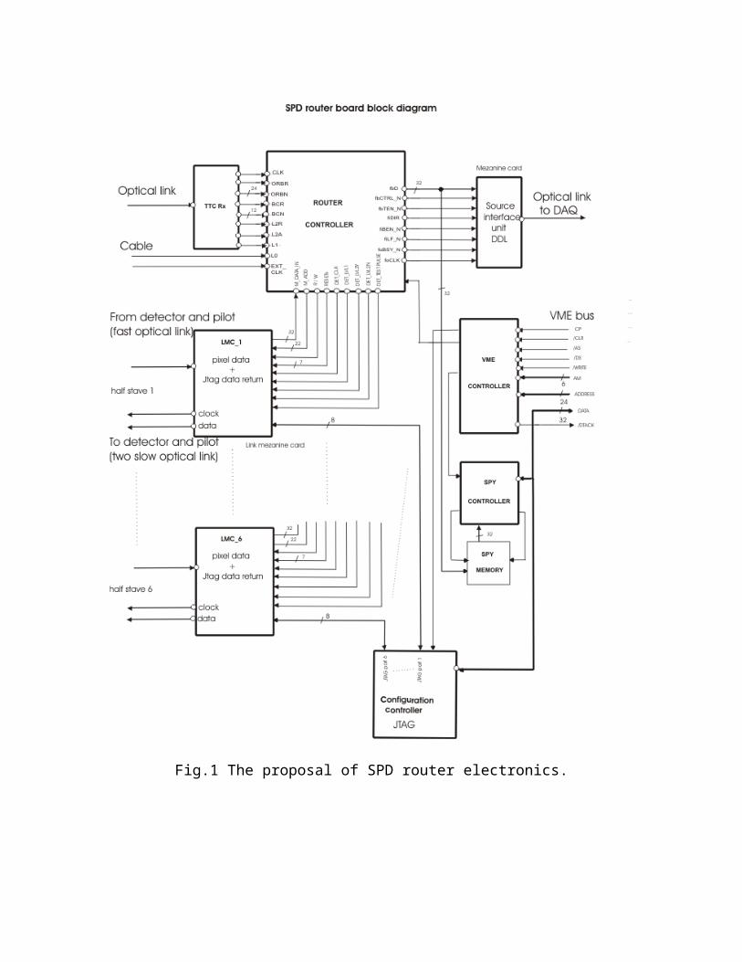
Fig.1 The proposal of SPD router electronics.
This block diagram (Fig. 1.) shows the proposal of router electronics as it is created by electronics group from Institute of Experimental physics in Kosice in collaboration with CERN pixel group. Source interface unit ( SIU-DDL [1]) and Link mezanine card ( LMC [2]) components will be delivered from CERN group and interfaced to router board as mezanine cards.
Signals used for SPD router.
Signals received from trigger: - 40.08MHz clock- BCR- BCN [11:0]- ORBR ( INIT )- ORBN - ECR
- L1 - L2Y
- L2N- L0 /over cable/
- CLK - 40.08MHz /over cable/
Signals sent to detectors and pilot: - RESET_CONTROL_RECEIVER ( over two slow optical links ) (INIT: Control link)
- RESET_GLOBAL (GOL, pixel, pilot) - RESET_GOL - RESET_pixel - TRST_pixel ( JTAG, pixel) - TRST_standard_on (JTAG, pixel, GOL) - TRST_standard_off (JTAG, pixel, GOL)
- DET_CLK ( must be connected with clock from external cable )
- DET_LVL1 - DET_LVL2Y - DET_LVL2R - DET_TEST_PULSE
- TCK (JTAG) - TMS (JTAG)
- TDI (JTAG) - M_ADD [21..0] - R/W
Signals received from detectors and pilot: - DATA_IN [31..0] ( over one fast optical link ) (Control word 0, Control word 1, event data)
- TRST_ret- TCK_ret- TMS_ret- TDO_ret
Signals for communication with SIU-DDL: - fbD [31..0]- fbCTRL_N- fbTEN_N
- fiDIR - fiBEN_N
- fiLF_N - foBSY_N - foCLK
ROUTER controller - sends trigger control signals, RESET signals and signals for communication with
Pixel converter daughter board to 6 LMC buses. - receives pixel data, Jtag return data a control signals from 6 LMC buses.
Data are formatted, filtered and labeled with trigger identification information.The router creates and arranges queues from different physical events.
In idle state router is waiting for L0. Than router is waiting for L1 (L1 timeout is 6 s). After the receipt of L1 router is waiting for L2Y or L2N. If router receives L2Y then will check event ready bit and link ready bit ( bit 0 and bit 16 in control_word_0 ) in all 6 LMC in sequence from LMC 0 to LMC 5. The assertion of this bit indicates a presence of at least one event and that no errors were present. In this case data will be read out from corresponding LMC and router is reading the start and the end address from control_word_1. Using these addresses the event data will read out and router will assert the flush event register in order to delete corresponding event data from pilot memory.If router receives L2N, than it will assert the flush event register directly and data will not be read out from pilot memory.Router will create header and trailer, which will be added to the corresponding pixel data and sent to DAQ over DDL. Data format is defined by figure 4. ROUTER controller is implemented in FPGA ( ALTERA EP20KE ) , programmed in Verilog Hardware Description Language and simulated with Quartus software ( from ALTERA corporation ).
Configuration controller – (JTAG) is being used to load configuration of Pixel chips. JTAG data are sent to detector over slow optical link and receive data being returned from Pixel Detector over fast optical link.
In IDLE state JTAG_controller is waiting for Execution_start, which will start JTAG_master_state_machine. The input buffer FIFO_IN must be filled written data, before one asserts Execution start. The failure of doing so will result in ERROR_1 (bit 9 in STATUS register). JTAG_controller processes marcoinstructions which are stored in
FIFO_IN and data are sent to corresponding JTAG channel. Returned data ( from TDO ) are stored in FIFO_OUT and can be read out via VME. ERROR_4 (bit 31 in STATUS register) appears when FIFO_OUT is full and one want to write data to this buffer. ERROR_3 (bit 17 in STATUS register) appears when controller wants read trailer and there is not trailer.ERROR_2 (bit 11 in STATUS register) appears when controller wants read control_word_ 2 and there is header.
JTAG controller is implemented in FPGA ( ALTERA EP20KE) , designed with Verilog Hardware Description Language and simulated with Quartus software ( from ALTERA corporation ).
SPY controller maintains a copy of data samples sent to DAQ system. These data are stored in the SPY memory and can be accessed via VME interface.The stored data can be used for monitoring and test purposes.
SPY controller is implemented in FPGA ( ALTERA EPM3128A) , programmed in Verilog Hardware Description Language and simulated with MAX PLUS + software ( from ALTERA corporation ). The SPY memory itself is high-speed (3.3V 32Kx36) synchronous pipelined dual-port RAM ( IDT 70V3579S).
VME controller – handles VME access for JTAG controller, Router controller and SPY controller.
VME controller is implemented in FPGA ( ALTERA EPM7064 ) , programmed in Verilog Hardware Description Language and simulated with MAX PLUS + software ( from ALTERA corporation ).
Fig. 2. The Router header and trailer.
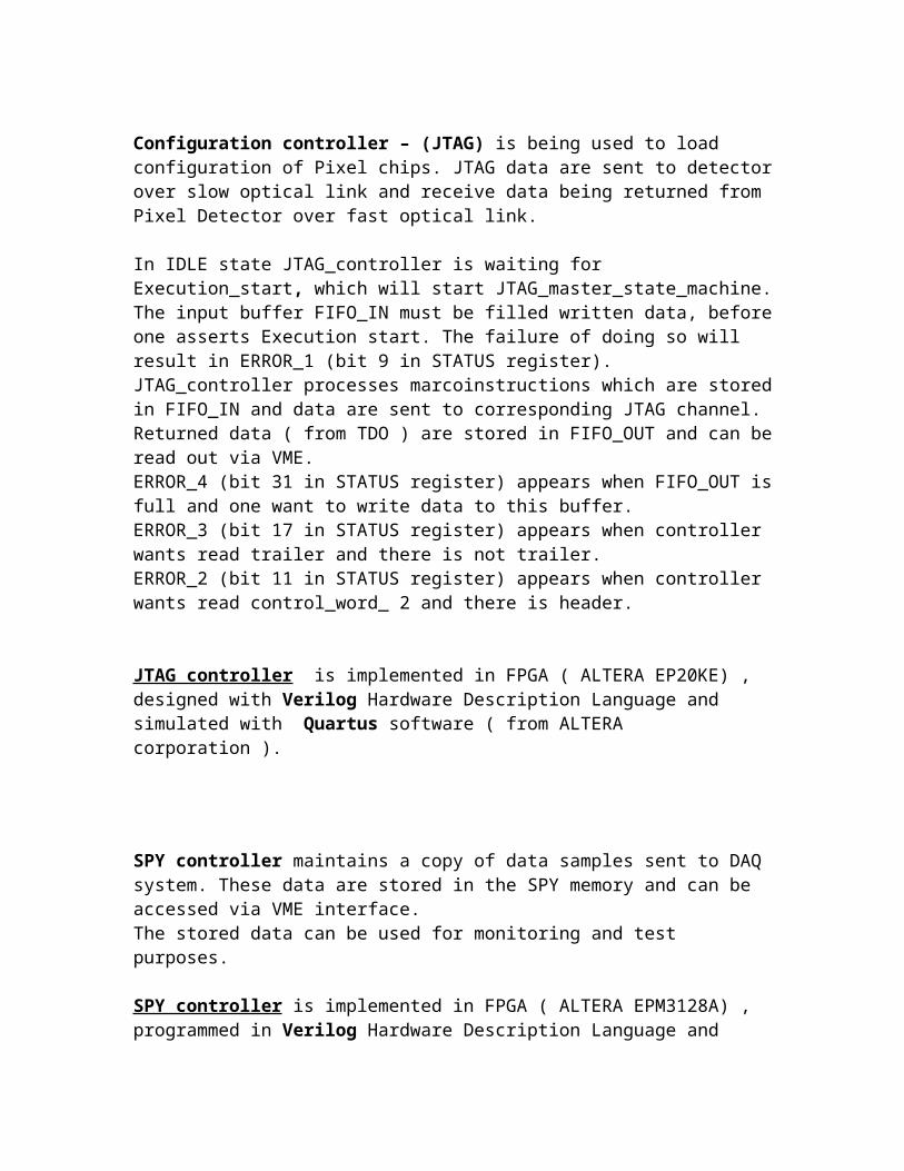
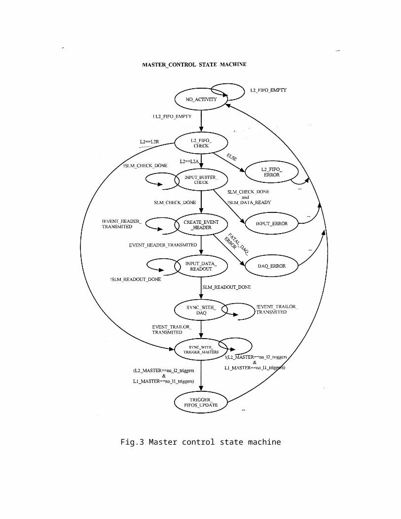
Fig.3 Master control state machine
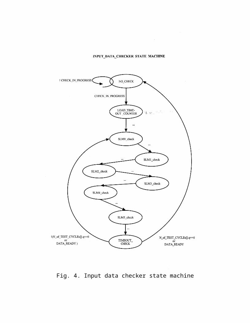
Fig. 4. Input data checker state machine
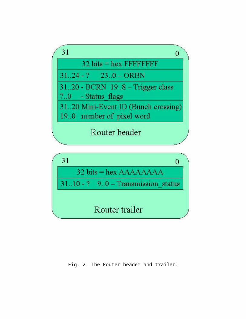
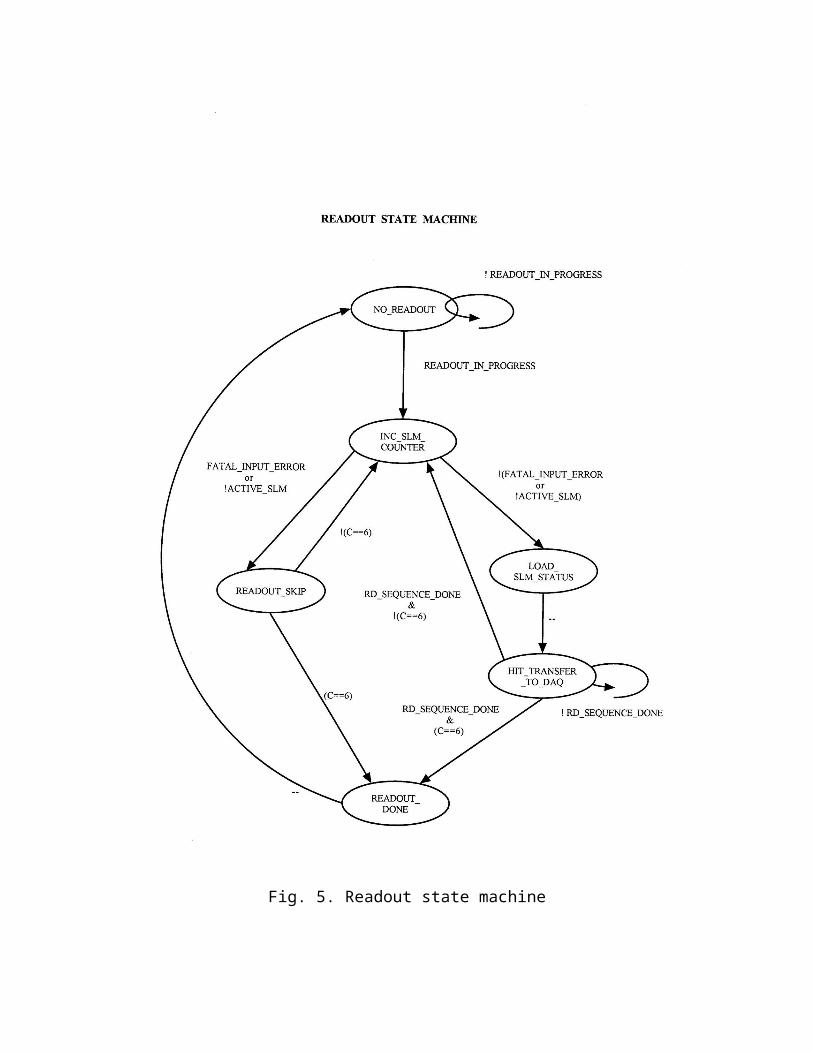
Fig. 5. Readout state machine

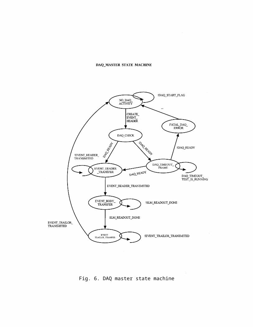
Fig. 6. DAQ master state machine
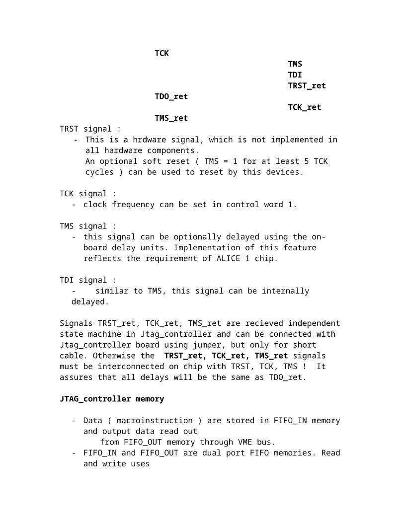
JTAG controller
Fig. 7. Functional block diagram of JTAG controller.
This block diagram shows the fundamentals of Configuration controller designed by electronics group IEP SAS Kosice. The controller will be incorporated into SPD Router 9U board.
Base signal used for communication with pixel chip: TRST
TCK TMS TDI TRST_ret
TDO_ret
TCK_retTMS_ret
TRST signal :- This is a hrdware signal, which is not implemented in all hardware components.
An optional soft reset ( TMS = 1 for at least 5 TCK cycles ) can be used to reset by this devices.
TCK signal :- clock frequency can be set in control word 1.
TMS signal :- this signal can be optionally delayed using the on-board delay units.
Implementation of this feature reflects the requirement of ALICE 1 chip.
TDI signal :- similar to TMS, this signal can be internally delayed.
Signals TRST_ret, TCK_ret, TMS_ret are recieved independent state machine in Jtag_controller and can be connected with Jtag_controller board using jumper, but only for short cable. Otherwise the TRST_ret, TCK_ret, TMS_ret signals must be interconnected on chip with TRST, TCK, TMS ! It assures that all delays will be the same as TDO_ret.
JTAG_controller memory
- Data ( macroinstruction ) are stored in FIFO_IN memory and output data read out from FIFO_OUT memory through VME bus.- FIFO_IN and FIFO_OUT are dual port FIFO memories. Read and write uses different clocks – read and write cycles are independent.
JTAG_ports
- Data can be sent to one of the 6 ports implemented in JTAG controller.- Port can be selected in Control word 1 ( bits 10..8 ) and number of port is 0 – 5.
Default port is port number 0. - Every macroinstruction can be sent to different port. Each macroinstruction can
be also scanned at different speed.
JTAG_instructions
- There are 3 fundamental instructions executed by the controller:1. IR Scan 2. DR Scan3. RESET
- Type of instruction can be set in control word 1 ( bits 7..0 ) as 2 for RESET instruction
4 for DR Scan 5 for IR Scan
Clock Speed
- Main controller operates at a frequency of 10 MHz.- Clock for JTAG channels can be set in control word 1( bits 15..12 ), up to 5 MHz.- Default clock speed is the slowest - 312,5 kHz.- Option for clock speed if clock number is 4 - 5 Mhz
3 - 2,5 MHz 2 - 1,25 Mhz 1 - 625 kHz other - 312.5 kHz.
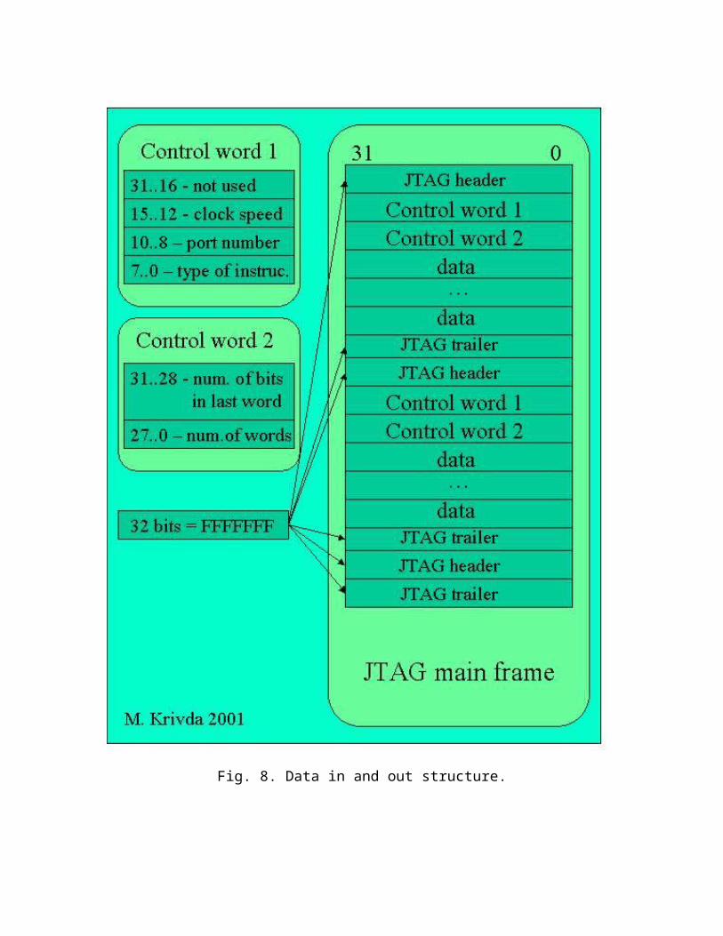
Data format
- Macroinstructions and output data are 32 bits words. - The macroinstructions are defined by DATA_IN_STRUCTURE and the output
data are defined by DATA_OUT_ STRUCTURE. It is same structure, but data are different.
- Structure of the header and trailer is identical for both the macroinstructions and the output data.
Header and trailer:
Bits hex format31..0 FFFFFFFF
Control word 1:
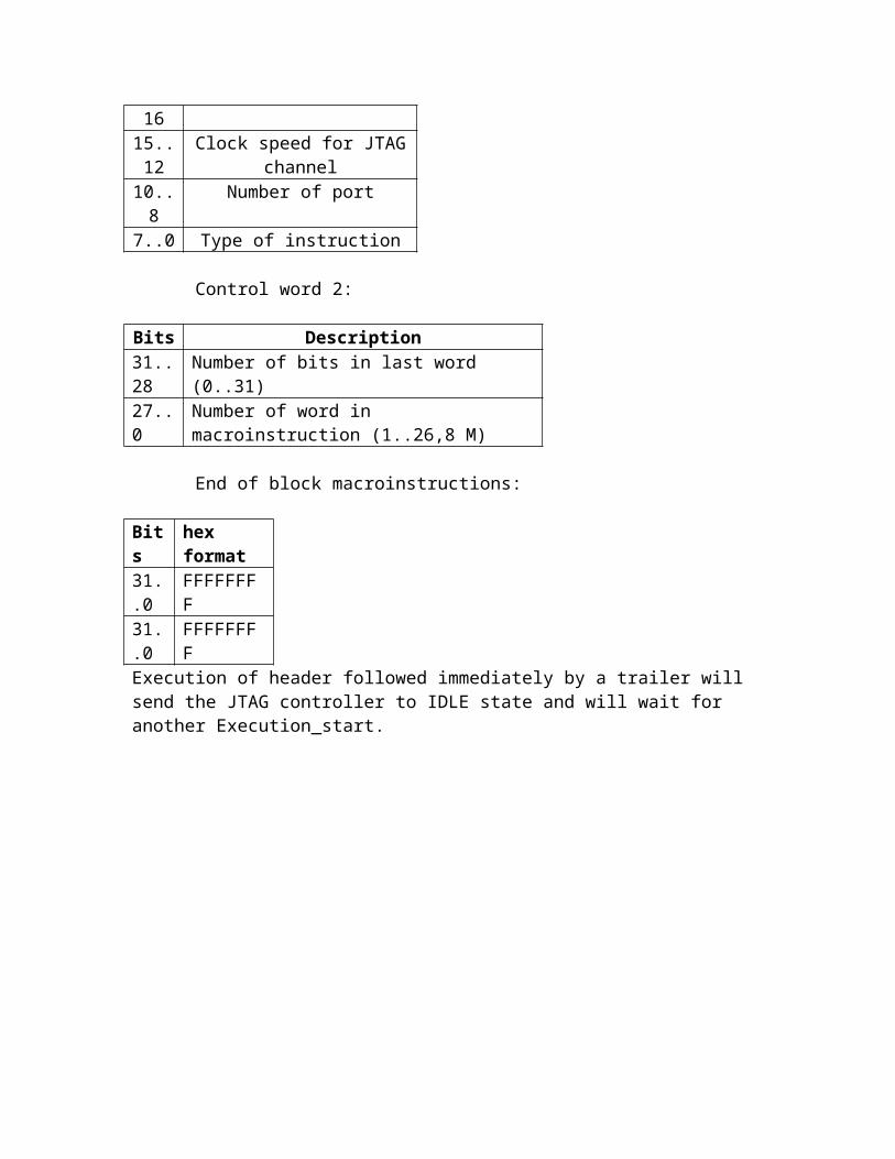
Bits Description31..16 Not used15..12 Clock speed for JTAG channel10..8 Number of port7..0 Type of instruction
Control word 2:
Bits Description31..28 Number of bits in last word (0..31)27..0 Number of word in macroinstruction (1..26,8 M)
End of block macroinstructions:
Bits hex format31..0 FFFFFFFF31..0 FFFFFFFF
Execution of header followed immediately by a trailer will send the JTAG controller to IDLE state and will wait for another Execution_start.
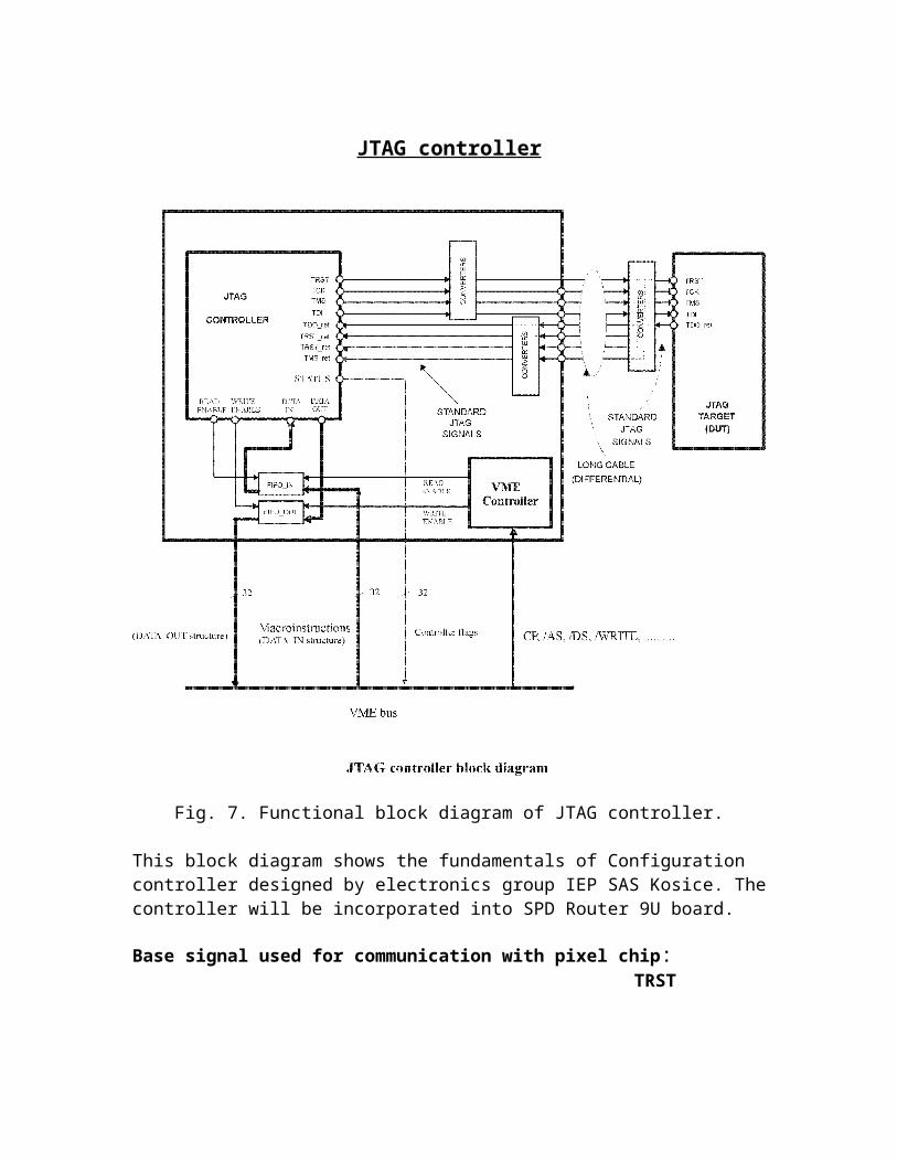
Fig. 8. Data in and out structure.
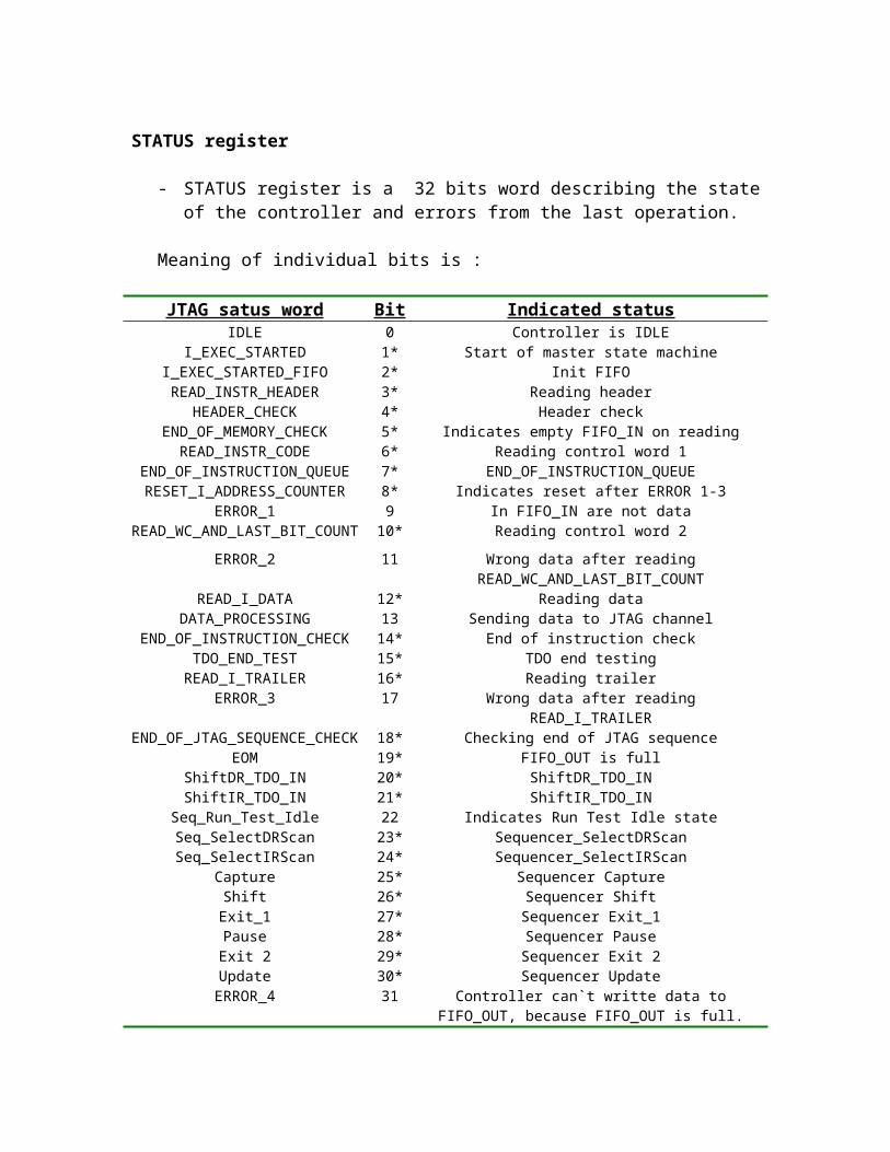
STATUS register
- STATUS register is a 32 bits word describing the state of the controller and errors from the last operation.
Meaning of individual bits is :
JTAG satus word Bit Indicated statusIDLE 0 Controller is IDLE
I_EXEC_STARTED 1* Start of master state machine I_EXEC_STARTED_FIFO 2* Init FIFOREAD_INSTR_HEADER 3* Reading header
HEADER_CHECK 4* Header check END_OF_MEMORY_CHECK 5* Indicates empty FIFO_IN on readingREAD_INSTR_CODE 6* Reading control word 1
END_OF_INSTRUCTION_QUEUE 7* END_OF_INSTRUCTION_QUEUERESET_I_ADDRESS_COUNTER 8* Indicates reset after ERROR 1-3
ERROR_1 9 In FIFO_IN are not dataREAD_WC_AND_LAST_BIT_COUNT 10* Reading control word 2
ERROR_2 11 Wrong data after reading READ_WC_AND_LAST_BIT_COUNT
READ_I_DATA 12* Reading dataDATA_PROCESSING 13 Sending data to JTAG channel
END_OF_INSTRUCTION_CHECK 14* End of instruction checkTDO_END_TEST 15* TDO end testingREAD_I_TRAILER 16* Reading trailer
ERROR_3 17 Wrong data after reading READ_I_TRAILER
END_OF_JTAG_SEQUENCE_CHECK 18* Checking end of JTAG sequenceEOM 19* FIFO_OUT is full
ShiftDR_TDO_IN 20* ShiftDR_TDO_INShiftIR_TDO_IN 21* ShiftIR_TDO_IN
Seq_Run_Test_Idle 22 Indicates Run Test Idle stateSeq_SelectDRScan 23* Sequencer_SelectDRScanSeq_SelectIRScan 24* Sequencer_SelectIRScan
Capture 25* Sequencer CaptureShift 26* Sequencer ShiftExit_1 27* Sequencer Exit_1Pause 28* Sequencer PauseExit 2 29* Sequencer Exit 2Update 30* Sequencer UpdateERROR_4 31 Controller can`t writte data to
FIFO_OUT, because FIFO_OUT is full.
* These bits are used for debugging of JTAG controller and they will change to useful information .
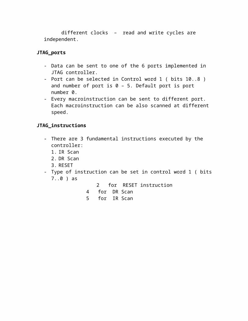
Fig. 9. Main state machine of JTAG controller
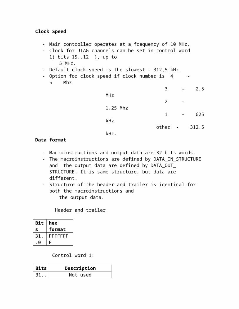
Fig. 10. State machine for generation a TMS sequence.
Design of JTAG_controller is compliant with IEEE Standard Test Access Port and Boundary-Scan Architecture ( IEEE Std 1149.1-1990 ).
The VME JTAG assumes A24/D32 transfers. All data from described registers are 32 bits, but only few bits are really necessary from some registers.
VME address of board can be set on board by hexadecimal switch: IC 22 ( 4 valid bits ) IC23 ( only 1 valid bit - most significant in the address: A23 bit) VME address allocation:
Write data Write-only 0x074000Read data Read-only 0x070000Execution_start Write-only 0x078000Read status JTAG controller Read-only 0x068000Read status FIFOs Read-only 0x06c000RESET_JTAG_controller Write-only 0x07c000RESET_FIFOs Write-only 0x08c000Reset_JTAG_channel_0 Write-only 0x064000Reset_JTAG_channel_1 Write-only 0x060000Reset_JTAG_channel_2 Write-only 0x05c000Reset_JTAG_channel_3 Write-only 0x058000
Jumpers on the board: Jumpers for bip./dif. switching : - for bipolar signals is jumper OFF
- for differential signals is jumper ONJumper J15 is used manual reset.
Jumpers for connection signals TRST_ret, TCK_ret, TMS_ret with signals TRST, TCK, TMS.
Test of JTAG controller
1. Standalone test controller with short circuit a connection TDI – TDO with 10 000 testing loops.
DR instruction sent – 0 errors .IR instruction sent – 0 errors .Combination of DR and IR instructions sent – 1 error in 2 000 – 10 000 loops.
2. Testing with the DAQ adaptor board with 100 loops.Test motherboard - ON, OFF is O.K.Set any voltage - O.K.
3. Testing with the pixel board.Set global register 5 with value 170 – 1 error in 1000 loops.
Status of the Router electronics for Alice SPD ( november 2001 ).
A/ Router Controller
Status: Altera code written ( in Verilog HDL) for the interface between the pixel detector and the router as defined in April 2001.Next action/step: Cern group is working on update document ”Interface between pilot and router”. Once new interface will be defined the code need to be adopted.
B/ Configuration controller – JTAG
Status: Altera code written (in Verilog HDL) and extensively simulated. First prototype produced and tested. Controller was tested with MB board and pixel chip board and some errors were eliminated.
Next action/step: Before producing second version of the board we must complete the first version of the board with successful loading all the registers of pixel chip. Still pixel registers loading to be tested.
There is an random error, which will be corrected. We have to correct mistakes which occur in first prototype and will produce the correct version .
C/ Spy memory controller
Status: Altera code written and simulated.