Embed Size (px)
Citation preview

Kuliah MikrokontrolerKuliah MikrokontrolerAVRAVR
ADC AVRADC AVR
Eru©September 2009Eru©September 2009
PENSPENS

ADCADC8 Channel ADC 8 Channel ADC MultiplexedMultiplexed– 8 Single-ended8 Single-ended– 2 Differential with 2 Differential with
Programmable Gain at 1x, Programmable Gain at 1x, 10x, or 200x10x, or 200x
8/10 bit resolution8/10 bit resolutionVariable Clock SpeedVariable Clock SpeedVarious Reference VoltageVarious Reference VoltageFree/Controlled RunningFree/Controlled RunningPolling/Interrupt EOCPolling/Interrupt EOCNoise ReductionNoise Reduction


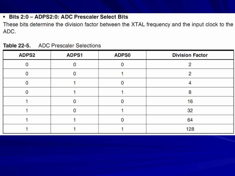
ADC Clock – clkADCADC Clock – clkADC
The ADC is provided with a dedicated The ADC is provided with a dedicated clock domain.clock domain.
This allows halting the CPU and I/O clocks This allows halting the CPU and I/O clocks in order to reduce noise generated by in order to reduce noise generated by digital circuitry.digital circuitry.
This gives more accurate ADC conversion This gives more accurate ADC conversion results.results.

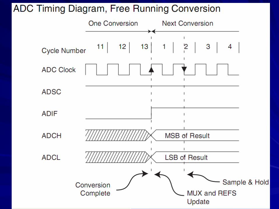
FeaturesFeatures10-bit Resolution10-bit Resolution0.5 LSB Integral Non-linearity0.5 LSB Integral Non-linearity±2 LSB Absolute Accuracy±2 LSB Absolute Accuracy13 - 260 µs Conversion Time13 - 260 µs Conversion TimeUp to 15 kSPS at Maximum ResolutionUp to 15 kSPS at Maximum Resolution8 Multiplexed Single Ended Input Channels8 Multiplexed Single Ended Input Channels7 Differential Input Channels7 Differential Input Channels2 Differential Input Channels with Optional Gain of 10x and 200x(1)2 Differential Input Channels with Optional Gain of 10x and 200x(1)Optional Left adjustment for ADC Result ReadoutOptional Left adjustment for ADC Result Readout0 - VCC ADC Input Voltage Range0 - VCC ADC Input Voltage RangeSelectable 2.56V ADC Reference VoltageSelectable 2.56V ADC Reference VoltageFree Running or Single Conversion ModeFree Running or Single Conversion ModeADC Start Conversion by Auto Triggering on Interrupt SourcesADC Start Conversion by Auto Triggering on Interrupt SourcesInterrupt on ADC Conversion CompleteInterrupt on ADC Conversion CompleteSleep Mode Noise CancelerSleep Mode Noise Canceler
Note: 1. The differential input channels are not tested for devices in PDIP Note: 1. The differential input channels are not tested for devices in PDIP Package. This feature is only guaranteed to work for devices in TQFP and Package. This feature is only guaranteed to work for devices in TQFP and QFN/MLF PackagesQFN/MLF Packages


ADC Conversion ResultADC Conversion Result
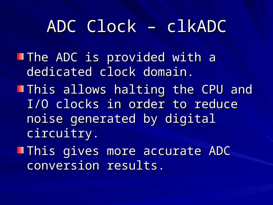
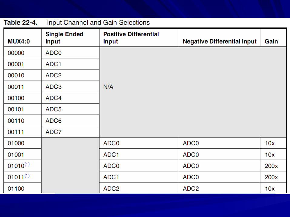
After the conversion is complete (ADIF is high), After the conversion is complete (ADIF is high), the conversion result can be found in the ADCthe conversion result can be found in the ADCResult Registers (ADCL, ADCH). Result Registers (ADCL, ADCH). For single ended conversion, the result isFor single ended conversion, the result iswhere VIN is the voltage on the selected input where VIN is the voltage on the selected input pin and VREF the selected voltage reference pin and VREF the selected voltage reference (see(seeTable 22-3 on page 221 and Table 22-4 on page Table 22-3 on page 221 and Table 22-4 on page 222). 0x000 represents ground, and 0x3FF222). 0x000 represents ground, and 0x3FFrepresents the selected reference voltage minus represents the selected reference voltage minus one LSB.one LSB.
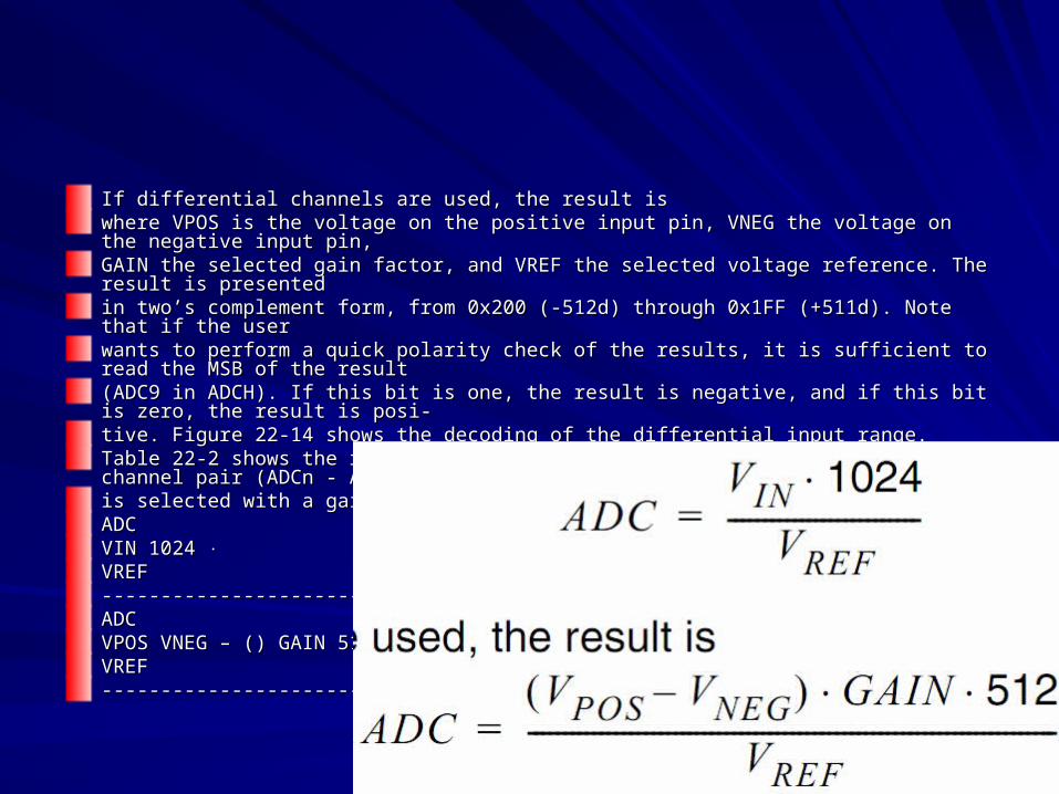
If differential channels are used, the result isIf differential channels are used, the result iswhere VPOS is the voltage on the positive input pin, VNEG the voltage on the negative input pin,where VPOS is the voltage on the positive input pin, VNEG the voltage on the negative input pin,GAIN the selected gain factor, and VREF the selected voltage reference. The result is presentedGAIN the selected gain factor, and VREF the selected voltage reference. The result is presentedin two’s complement form, from 0x200 (-512d) through 0x1FF (+511d). Note that if the userin two’s complement form, from 0x200 (-512d) through 0x1FF (+511d). Note that if the userwants to perform a quick polarity check of the results, it is sufficient to read the MSB of the resultwants to perform a quick polarity check of the results, it is sufficient to read the MSB of the result(ADC9 in ADCH). If this bit is one, the result is negative, and if this bit is zero, the result is posi-(ADC9 in ADCH). If this bit is one, the result is negative, and if this bit is zero, the result is posi-tive. Figure 22-14 shows the decoding of the differential input range.tive. Figure 22-14 shows the decoding of the differential input range.Table 22-2 shows the resulting output codes if the differential input channel pair (ADCn - ADCm)Table 22-2 shows the resulting output codes if the differential input channel pair (ADCn - ADCm)is selected with a gain of GAIN and a reference voltage of VREF.is selected with a gain of GAIN and a reference voltage of VREF.ADCADCVIN 1024 ⋅VIN 1024 ⋅VREFVREF-------------------------- =-------------------------- =ADCADCVPOS VNEG – () GAIN 512 ⋅⋅VPOS VNEG – () GAIN 512 ⋅⋅VREFVREF------------------------------------------------------------------------ =------------------------------------------------------------------------ =


Contoh AplikasiContoh Aplikasi


![[5] Bab 2 - thesis.binus.ac.idthesis.binus.ac.id/Doc/Bab2/2012-1-00641-sk 2.pdf · Mikrokontroler Pada alat yang dibuat ini, mikrokontroler yang dipakai adalah AVR yang berjenis ATMEGA1284P](https://img.pdfslide.net/doc/110x75/5b5cd2487f8b9ac6028d0602/5-bab-2-2pdf-mikrokontroler-pada-alat-yang-dibuat-ini-mikrokontroler-yang.jpg)