Embed Size (px)
Citation preview
“%kulqs
Final ReportSBIR Phase II - Bandgap-Engineered Thermophotovoltaic Devices for High
Efficiency Radioisotope PowerDOE Grant No: DE-FG03-95ER81957/AOO0
TECHNICAL OBJECTIVES OF PHASE H RESEARCH
During Phase I effort, we demonstrated the fabrication of GaInAsSb photovoltaic (W)cells by the diffused junction process. The feasibility of growing bulk GaInAsSb crystals by thetraveling heater method (THM) method was also demonstrated. The key issues of the Phase IIwork will be the perfection of the diffused junction cell fabrication process, the demonstration of alarge scale THM crystal growth capability, and the demonstration of long wavelength cells in twoprototype thermophotovoltaic (lTV) applications. We have set the following specific technicalobjectives for the Phase II effort
Scale up the THM bulk crystal growth.
Optimim the diffused junction GaInAsSb cell fabrication process a) using epitaxially grownquatermry layers on GaSb wafers, b) THM grown quaternary wafers, and c) processepitaxially grown GaIhAsSb p/n junctions into TPV cells and evaluate their performancerelative to diffused junction devices.
Optimize a resonant metal mesh infrared (II?) filter for use with the long wavelength cells inTPV applications having emitter temperatures in the range between 800”C and 1000”C.
Demonstrate the pefiormance of GaInAsSb cells in a resistively heated RTPV testbed and in aprototype propane fueled commercial testbed.
Perform cost analyses of the production processes and test market the commercial prototype todetermine customer interest and pricing issues.
TECHNICAL APPROACH
The main objective of Phase Ii is to design and develop processes for manufacturing GaSbbased low bandgap photovoltaic devices and optimize IR filter production that meet the demands ofboth space and terrestrial TPV applications. The device manufacturing base developed in thisprogram can also be used for fabricating other III-V compound semiconductor such as GaAs basedsolar cells. Our technical approach in Phase II is to utilize the knowledge and experience gained inPhase I to develop a GaSb based quaternary low bandgap TPV cell manufacturing scheme. Wehave taken a three level approach to achieve this objective.
In the fust, in order to optimize the TPV device structure in terms of doping level,thickness and composition of the base and emitter layers we have contracted Research TriangleInstitute to grow such structures epitaxially on a GaSb substrate. The epi-grown wafers will beprocessed into photovoltaic devices and will help to define the ultimate performance capabilities ofthese low bandgap devices. These epi-grown high efficiency devices would be useful for spaceapplications.
The THM was established in Phase I as a simple technique for producing 1 cm diameterquaternary GfiAsSb materials. During this Phase II effort, a THM system has been setup atEDTEK and crystal growth being carried out to grow Te doped Ga.InAsSb crystals. This THMhas been scaled up to grow one inch diameter crystals and the results of this effort are summarizedbelow. Thin (about 500 micron thick) THM grown single crystal substrates will be used to
1
DISCLAIMER
This repofi was prepared as an account of work sponsoredby an agency of the United States Government. Neitherthe United States Government nor any agency thereof, norany of their employees, make any warranty, express orimplied, or assumes any legal liability or responsibility forthe accuracy, completeness, or usefulness of anyinformation, apparatus, product, or process disclosed, orrepresents that its use would not infringe privately ownedrights. Reference herein to any specific commercialproduct, process, or service by trade name, trademark,manufacturer, or otherwise does not necessarily constituteor imply its endorsement, recommendation, or favoring bythe United States Government or any agency thereof. Theviews and opinions of authors expressed herein do notnecessarily state or reflect those of the United StatesGovernment or any agency thereof.
DISCLAIMER
Portions of this document may be illegiblein electronic image products. Images areproduced from the best available originaldocument.
. . t
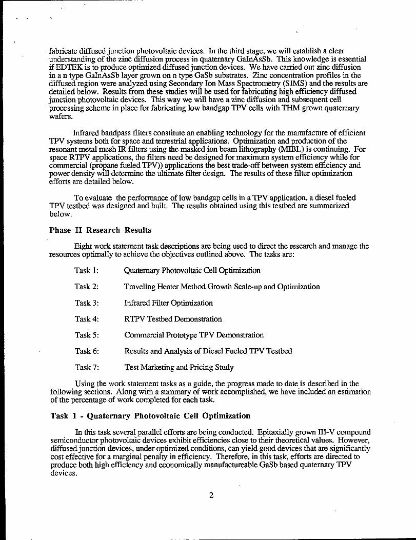
fabricate diffused junction photovoltaic devices. In the third stage, we will establish a clearunderstanding of the zinc diffusion process in quaternary GaInAsSb. This knowledge is essentialif EDTEK is to produce optimized diffused junction devices. We have carried out zinc diffusionin a n type GaInAsSb layer grown on n type GaSb substrates. Zinc concentration proffles in thediffused region were analyzed using Secondary Ion Mass Spectrometry (SIMS) and the results aredetailed below. Results ffom these studies will be used for fabricating high efilciency diffusedjunction photovoltaic devices. This way we will have a zinc diffusion and subsequent cellprocessing scheme in place for fabricating low bandgap TPV cells with THM grown quaternarywafers.
Inikared bandpass falters constitute an enabling technology for the manufacture of efficientTPV systems both for space and terrestrial applications. Optimization and production of theresonant metal mesh II? filters using the masked ion beam lithography (MIBL) is continuing. Forspace RTPV applications, the falters need be designed for maximum system efficiency while forcommercial (propane fueled TPV)) applications the best trade-off between system efficiency andpower density will determine the ultimate fflter design. The results of these falter optimizationefforts are detailed below.
To evaluate the performance of low bandgap cells in a TPV application, a diesel fueledTPV testbed was designed and built. The results obtained using this testbed are summarizedbelow.
Phase II Research Results
Eight work statement task descriptions are being used to direct the research and manage theresources optimally to achieve the objectives outlined above. The tasks are:
Task 1: Quaternary Photovoltaic Cell Optimization
Task 2: Traveling Heater Method Growth Scale-up and Optimization
Task 3: Infrared Filter Optimization
Task 4: RTPV Testbed Demonstration
Task 5: Commercial Prototype TPV Demonstration
Task 6: Results and Analysis of Diesel Fueled TPV Testbed
Task 7: Test Marketing and Pricing Study
Using the work statement tasks as a guide, the progress made to date is described in thefollowing sections. Along with a summary of work accomplished, we have included an estimationof the percentage of work completed for each task.
Task 1 - Quaternary Photovoltaic Cell Optimization
In this task several parallel efforts are being conducted. Epitaxially grown III-V compoundsemiconductor photovoltaic devices exhibit ef!fkiencies close to their theoretical values. However,diffused junction devices, under optimized conditions, can yield good devices that are significantlycost effective for a marginaI penalty in ef.llciency. Therefore, in this task, efforts are directed toproduce both high efficiency and economically manufacturable GaSb based quaternary TPVdevices.
2
. . ,
Task lb - Epitaxially Grown Cell Optimization
Through epitaxial techniques, it is possible to grow abrupt p-n junctions with individuallayers that have good morphology, precise doping and excellent electrical and opticalcharacteristics. It is also possible to introduce a back surface field by growing a higher bandgap n-type layer at the bottom of the base region in a p-on-n photovoltaic cell thereby augmenting theopen circuit voltage of the device. Grading the zinc doping profile in the emitter region has shownto improve the device performance due to dopant induced field. This task of epitaxial growth ofquaternary TPV devices is approximately 25% complete.
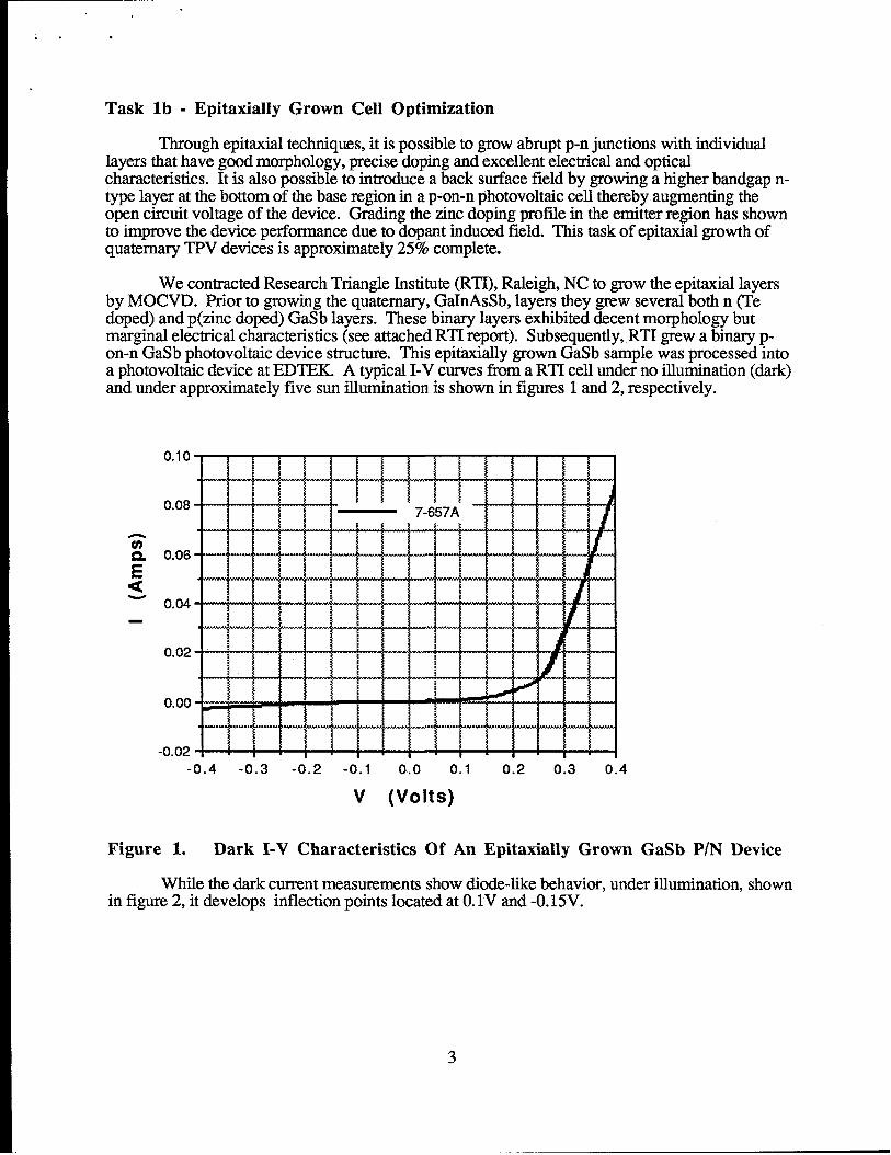
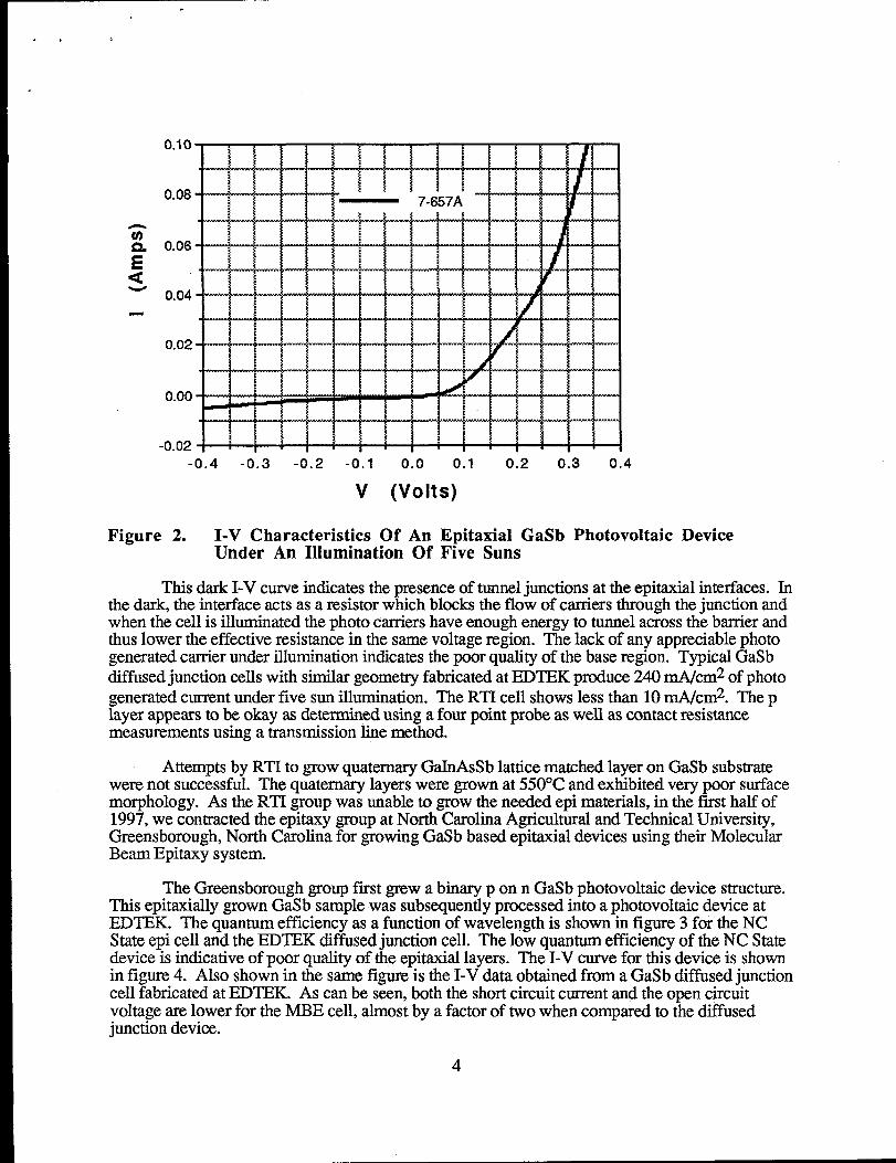
We contracted Research Triangle Institute (RTI), Raleigh, NC to grow the epitaxial layersby MOCVD. Prior to growing the quaternaxy, GaInAsSb, layers they grew several both n (Tedoped) and p(zinc doped) GaSb layers. These binary layers exhibited decent morphology butmarginal electrical characteristics (see attached RTI report). Subsequently, RTI grew a binary p-pen-nGaSb photovoltaic device structure. This epitaxially grown GaSb sample was processed intoa photovoltaic device at EDTEK. A typical I-V curves from a RTI cell under no illumination (dark)and under approximately five sun illumination is shown in figures 1 and 2, respectively.
E<w
0.10
0.08-— 7-657A
0.06-
0.04-
0.02-
0.00-
-0.02-0.4 -0.3 -0.2 -0.1 0.0 0.1 0.2 0.3 0.4
v (volts)
Figure 1. Dark I-V Characteristics Of An Epitaxially Grown GaSb P/N Device
While the dark current measurements show diode-like behavior, under illumination, shownin figure 2, it develops inflection points located at O.lV and -O.15V.
.
,. ‘
0.10
0.08
--0Q 0.06
E~
0.04
0.02
0.00
-0.02
— 7-657A
0.4 -0.3 -0.2 -0.1 0.0 0.1 0.2 0.3 0.4
v (volts)
Figure 2. I-V Characteristics Of An Epitaxial GaSb Photovoltaic DeviceUnder An Illumination Of Five Suns
This dark I-V curve indicates the presence of tunnel junctions at the epitaxial interfaces. Inthe dark, the interface acts as a resistor which blocks the flow of carriers through the junction andwhen the cell is illuminated the photo carriers have enough energy to tunnel across the barrier andthus lower the effective resistance in the same voltage region. The lack of any appreciable photogenerated carrier under illumination indicates the poor quality of the base region. Typical GaSbdiffused junction cells with similar geometry fabricated at EDTEK produce 240 mA/cm2 of photogenerated current under five sun illumination. The RTI cell shows less than 10 mA/cm2. The player appears to be okay as determined using a four point probe as well as contact resistancemeasurements using a transmission line method.
Attempts by RTI to grow quaternary GaInAsSb lattice matched layer on GaSb substratewere not successful. The quaternary layers were grown at 550°C and exhibited very poor surfacemorphology. As the RTI group was unable to grow the needed epi materials, in the first half of1997, we contracted the epitaxy group at North Carolina Agricultural and Technical University,Greensborough, North Carolina for growing GaSb based epitaxial devices using their MolecularBeam Epitaxy system.
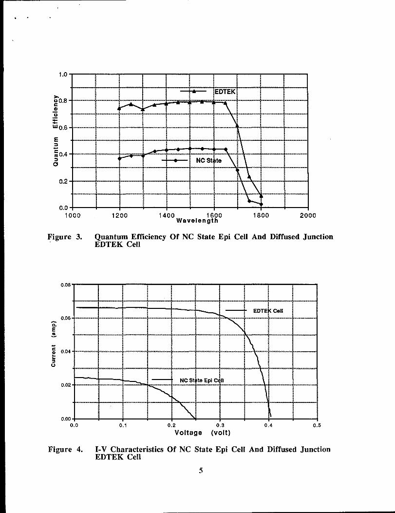
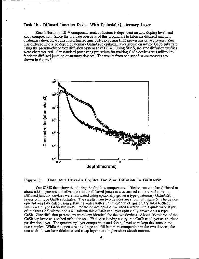
The Greensborough group fiist grew a binary p on n GaSb photovoltaic device structure.This epitaxially grown GaSb sample was subsequently processed into a photovoltaic device atEDTEK. The quantum efficiency as a fimction of wavelength is shown in figure 3 for the NCState epi cell and the EDTEK diffused junction cell. The low quantum efficiency of the NC Statedevice is indicative of poor quality of the epitaxial layers. The I-V curve for this device is shownin figure 4. Also shown in the same figure is the I-V data obtained from a GaSb diffused junctioncell fabricated at EDTEK As can be seen, both the short circuit current and the open circuitvoltage are lower for the MBE cell, almost by a factor of two when compared to the diffusedjunction device.
4
1000 1200 1400 1600 1800Wavelength
2000
Figure 3. Quantum Efficiency Of NC State Epi Cell And Diffused JunctionEDTEK Cell
0.08
0.06- —EEa
E@ o.04- —~
5
0.02- —
0.000.0 0.1 0.2 0.3 0.4 0.5
Voltage (volt)
Figure 4. I-V Characteristics Of NC State Epi Cell And Diffused JunctionEDTEK Cell
5
.- .
Task lb - Diffused Junction Device With Epitaxial Quaternary Layer
Zinc diffusion in III-V compound semiconductors is dependent on zinc doping level andalloy composition. Since the ultimate objective of this program is to fabricate diffused junctionquaternary devices, we first investigated zinc diffusion using LPE grown quaternary layers. Zincwas diffused into a Te doped quatemary Ga.InAsSb epitaxial layer grown on n-type GaSb substrateusing the pseudo-closed box diffusion system at EDTEK. Using SIMS, the zinc diffusion profileswere characterized. Our standard processing procedure for making GaSb devices was utilized tofabricate diffused junction quatemary devices. The results horn one set of measurements areshown in figure 5.
lC?
1$
,~
Id
,~
,~
,~51 I I0.0 1.0
Depth(microns)
Figure 5. Dose And Drive-In Profiles For Zinc Diffusion In GaInAsSb
Our SIMS data show that during the first low temperature diffusion run zinc has diffused toabout 600 angstroms and after drive-in the diffused junction was formed at about 0.5 micron.Diffused junction devices were fabricated using epitaxially grown n type quatemary GaInAsSblayers on n type GaSb substrates. The results from two devices are shown in figure 6. The deviceepi- 184 was fabricated using a starting wafer with a 3.9 micron thick quatema.ry InGaAsSb epilayer on a n type GaSb substrate. For the device epi-179 we used a wafer with a quaternary layerof thickness 2.5 micron and a 0.1 micron thick GaSb cap layer epitaxially grown on a n typeGaSb. Zinc diffusion parameters were kept identical for the two devices. About .06 micron of theGaSb cap layer was etched off in the epi-179 device leaving a very thin GaSb cap layer as a surfacepassivation layer. The quaternary layer composition and doping level were kept the same in thetwo samples. While the open circuit voltage and fdl factor are comparable in the two devices, theone with a lower base thickness and a cap layer has a higher short-circuit current.
6
.-
Attempts by the Greensborough group to grow epitaxial quaternary GaInAsSb layers onGaSb substrate were also not successful. In figure 7 we show the transmittance through aquaternary layer grown by the Greensborough group in their MBE facility. For comparison wealso show similar data for the quaternary grown by LPE. While the LPE sample shows a sharp cutoff at the band edge, the drop in absorption is gradual for the MBE sample indicative of aquatemary layer with varying composition. Thus in spite of their best efforts, both the RTI and theGreensborough groups were not successful in growing good quality (electrical&optical) binary,GaSb or quaternary, GaInAsSb layers.
0.06
0.05 -
0.04 -
0.03 -
0.02 -
0.01 -
0.000.0 0.1 0.2 0.3
Voltage (volt)
Figure 6. Current/Voltage Characteristics For Devices 184 And 179 UnderSimilar Illumination
1.2
nm
“: 1.0
xik(m
‘0.8
c
a0.4-
0.21900 2000 2100 2200 2300 2400 2500 2600
Wavelength (rim)
Figure 7. Variation Of Absorption As A Function Of Wavelength For AQuaternary Epi Layer Grown By MBE And LPE
Task lC - Diffused Junction Devices With Bulk Quaternary Crystals
Under this task we proposed to study zinc diffusion in THM grown bulk quaternarycrystals and also process zinc diffused quaternary devices. Details of THM growth apparatus set-up, scale-up and quatemary GaInAsSb crystal growth are detailed in the next task. Amistar, themanufacturer of THM crystal growth equipment provided EDTEK with several 1 cm diameterquatemary substrates as part of our contract. However, these substrates contained large number ofinclusions and electrode probe measurements showed that iridium and gallium are the mainconstituents in these inclusions. Attempts to diffuse zinc into these wafers were unsuccessfulbecause of the inclusions. Using the THM system installed at EDTE~ we were able to grow aone inch diameter n type quatemary boule. This boule was polycrystalline also with a number ofinclusions. Zinc was diffused into a wafer from this boule to form a p/n device. Thecharacteristics of this device are detailed in Task 2.
Task ld - Fabricate Thermophotovoltaic Cells for Demonstration Tests
This task calls for processing of epi-grown and diffused junction wafers into TPV cells foruse in demonstration tests. Lack of THM grown bulk quatemary substrates as well as epitaxialquatemary layers impeded the progress of this task.
Task 2 - Traveling Heater Method Growth Scale-up and Optimization
Scale-ut) of the Growth Format to 2.5 cm Diameter
The THM station was delivered to EDTEK, and became operational in the first quarter of1998. The 2.5 cm diameter format was used for all TKM runs. Several growth runs were carriedout at EIYTEKvarying such parameters as pull rate, temperature of the hot zone etc. Amistar ASOran several growth runs in their facility. EDTEK personnel received training horn Am.istsr, both atAmistar’s facility and at EDTEK. Amistar personnel have instructed EDTEK personnel intechniques and theory of THM crystal growth. The larger diameter material was also plagued bysoxneof the same problems that appeared in the 1 cm runs. Some metal inclusions were stillpresent, the growth became polycrystalline, and arsenic content gradually increased during the run.However, these problems were not quite so severe in the larger diameter runs, and no newproblems related to scale-up alone have appeared.
Omimization of Growth Parameters
Attempts to improve the quality of the THM quatemary material were largely unsuccessful.Slices from the second THM run at EDTEK (E2) are the best so far, of any quatemary materialgrown at EDTEK or Amistar. One of the slices from run E2 was used to make a diode; this deviceshowed rectifying behavior.
Material obtained from the first run at EDTEK (El) and ilom recent runs at Amistar (e.g.,A39, A40), has been of consistent quality, although rnicm structural defects (voids, metallicinclusions, fine cracks) prohibited fabrication of even a simple device on this material.
Review of literature dealing with THM and liquid phase epitaxy (LPE) of III-V alloysemiconductors indicated that slowing the growth rate of our THM material should result inimproved quality, in terms of fewer metallic inclusions, and fewer and larger grains. Thus, forE2, the growth rate was set at 1.1 mm/day, down from 2.5 mm/day, which was the rate used onall previous runs. E2 material is essentially free of cracks, has a lower volume fraction of metallicinclusions, and larger grains. Although a pristine area large enough for the fabrication of a TPVcell could not be found on the wafers, some of the wafer was suitable for making smaller devices.
The optical band edge of the THM material, as shown in figure 8, was found to be locatedat about 2100 nm, as determined by absorption measurements.
X-ray microprobe fluorescence data shows composition of the grown material to roughlymatch that of the alloy corresponding to this band edge. Sheet resistivity of this material, asgrown, was around 8 mW per square, n-type (from Te doping of the source materials).
Slice 2 from E2 was subjected to our usual processing procedures, for fabrication ofseveral small diodes. PECVD silicon nitride was deposited on the wafer, to serve as a diffusionbarrier, and for surface passivation. Circular areas approximately 2 mm in diameter were openedfor Zn diffusion and were then covered with metal film for contacts. Sheet resistivity after the Zndiffusion was around 600 mW per square, p-type. An I-V curve from one of the diodes, showingrectifying behavior, is shown in figure 9.
1.4
1.2
1.0
0.8
0.6 I I I 1 I
2000 2100 2200 2300 2400 2500
Wavelength
Figure 8. Variation Of Absorption As A Function Of Wavelength For A THMGrown Quaternary
n
awu
o
Figure
0.6
0.4-
0.2-
0.o-
-0.2-
-0.4-
-0.6-0.3 -0.2 -0.1 0.0 0.1 0.2 0.3
volts (v)
9. P-N Junction Diode Fabricated From THM Grown GaInAsSb
10
. .
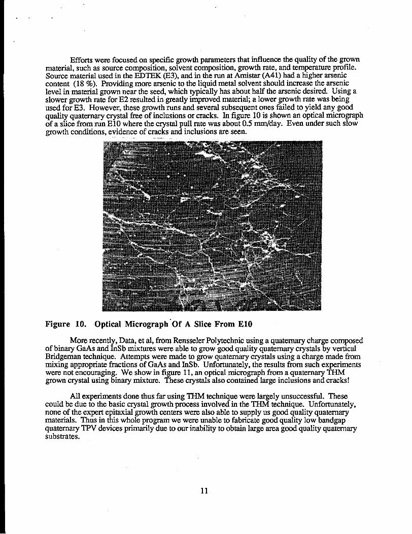
Efforts were focused on specific growth parameters that influence the quality of the grownmaterial, such as source composition, solvent composition, growth rate, and temperature profiie.Source material used in the EDTEK (E3), and in the run at Amistar (A41) had a higher arseniccontent (18 %). Providing more arsenic to the liquid metal solvent should increase the arseniclevel in material grown near the see& which typically has about half the arsenic desired. Using aslower growth rate for E2 resulted in greatly improved material; a lower growth rate was beingused for E3. However, these growth runs and several subsequent ones failed to yield any goodquality quaternary crystal free of inclusions or cracks. In figure 10 is shown an optical micrographof a slice from run E1O where the crystal pull rate was about 0.5 mm/day. Even under such slowgrowth conditions, evidence of cracks and inclusions are seen..-
Figure 10. Optical Micrograph “Of A Slice From E1O
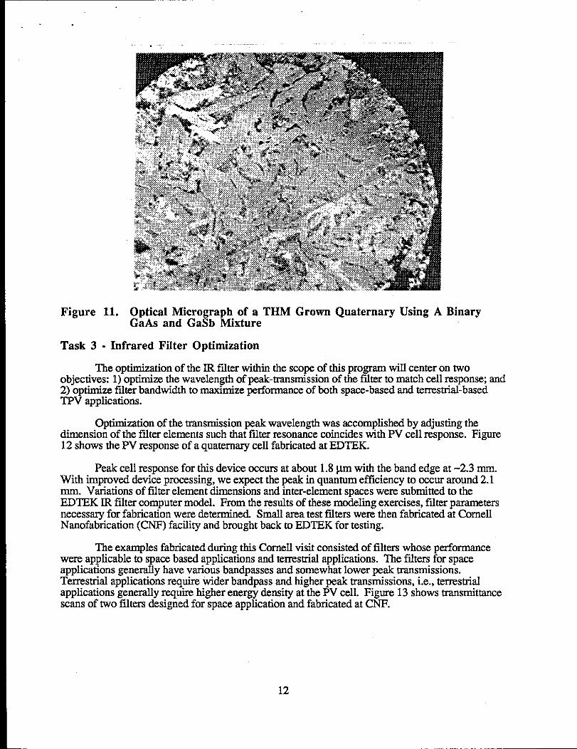
More recently, Data, et al, hm Rensseler Polytechnic using a quaternary charge composedof binary GaAs and InSb mixtures were able to grow good quality quaternary crystals by verticalBndgeman technique. Attempts were made to grow quatemary crystals using a charge made frommixing appropriate fractions of GaAs and InSb. Unfortunately, the results from such experimentswere not encouraging. We show in figure 11, an optical micrograph from a quaternary THMgrown crystal using binary mixture. These crystals also contained large inclusions and cracks!
All experiments done thus far using THM technique were largely unsuccessful. Thesecould be due to the basic crystal growth process involved in the THM technique. Unfortunately,none of the expert epitaxial growth centers were also able to supply us good quality quatemarymaterials. Thus in this whole program we were unable to fabricate good quality low bandgapquaternary TPV devices primarily due to our inability to obtain large area good quality quatemarysubstrates.
11
. .
Figure 11. Optical Micrograph of aTHM Grown Quaternary Using A BinaryGaAs and GaSb Mixture
Task 3- Infrared Filter Optimization
The optimization of the IR fflter within the scope of this program will center on twoobjectives: 1) optimize the wavelength of peak-transmission of the falter to match cell response; and2) optimize filter bandwidth to maximize performance of both space-based and terrestrial-basedTPV applications.
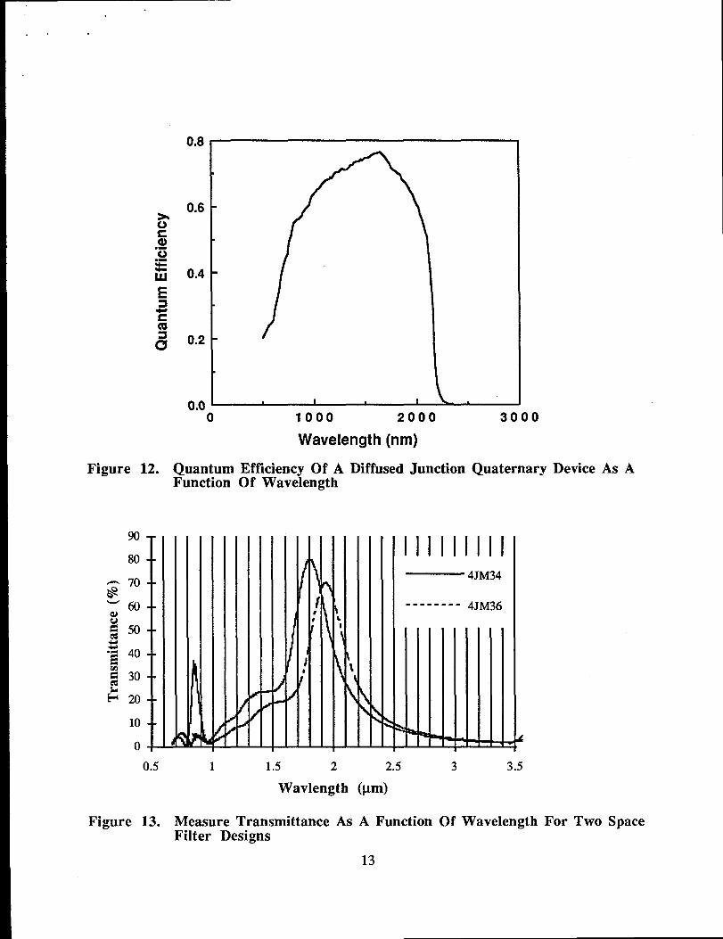
Optimization of the transmission peak wavelength was accomplished by adjusting thedimension of the filter elements such that filter resonance coincides with PV cell response. Figure12 shows the PV response of a quaternary cell fabricated at EDTEK.
Peak cell response for this device occurs at about 1.8 p.mwith the band edge at -2.3 mm.With improved device processing, we expect the peak in quantum efficiency to occur around 2.1mm. Variations of falter element dimensions and inter-element spaces were submitted to theEDTEK IR filter computer model. From the results of these modeling exercises, falterparametersnecessmy for fabrication were determined. Small area test falters were then fabricated at CornellNanofabrication (CNF) facility and brought back to EDTEK for testing.
The examples fabricated during this Cornell visit consisted of filters whose performancewere applicable to space based applications and terrestrial applications. The falters for spaceapplications generally have various bandpasses and somewhat lower peak transmissions.Terrestrial applications require wider bandpass and higher peak transmissions, i.e., terrestrialapplications generally require higher energy density at the PV cell. Figure 13 shows transmittancescans of two filters designed for space application and fabricated at CNF.
12
. .
Figure 12.
90
80
- 70@p
; 50
“j 40
Ej 30
& 20
10
0[
0.5
Figure 13.
0.8
0.6
0.4
0.2
0.00 1000 2000 3000
Wavelength (rim)
Quantum Efficiency Of A Diffused Junction Quarternary Device As AFunction Of Wavelength
1
4
,
.
1111111114JM34
‘------- 4JM36
1.5 2 2.5 3 3.5
Wavlength (~m)
Measure Transmittance As A Function Of Wavelength For Two SpaceFilter Designs
13
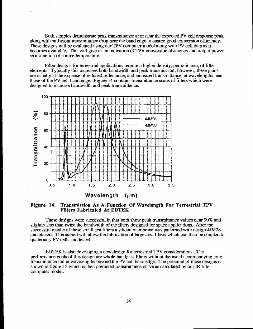
Both samples demonstrate peak transmittance at or near the expected PV cell response peakalong with sufficient transmittance drop near the band edge to ensure good conversion efficiency.These designs will be evaluated using our TPV computer model along with PV cell data as itbecomes available. This will give us an indication of TPV conversion efficiency and output poweras a function of source temperature.
Filter designs for terrestrial applications require a higher density, per unit area, of filterelements. Typically this increases both bandwidth and peak transmission, however, these gainsare usually at the expense of reduced reflectance, and increased transmittance, at wavelengths nearthose of the PV cell band edge. Figure 14 contains transmittance scans of filters which weredesigned to increase bandwidth and peak transmittance.
EUJsa
100
80
60
40
20
0
,.
0.5 1.0 1.5 2.0 2.5 3.0 3.5
Wavelength (pm)
Figure 14. Transmission As A Function Of Wavelength For Terrestrial TPVFilters Fabricated At EDTEK
These designs were successful in that both show peak transmittance values near 90% andslightly less than twice the bandwidth of the falters designed for space applications. After thesuccessful results of these small test falters a silicon membrane was patterned with design 4JM28and etched. This stencil will allow the fabrication of large area falters which can than be coupled toquaternary PV cells and tested.
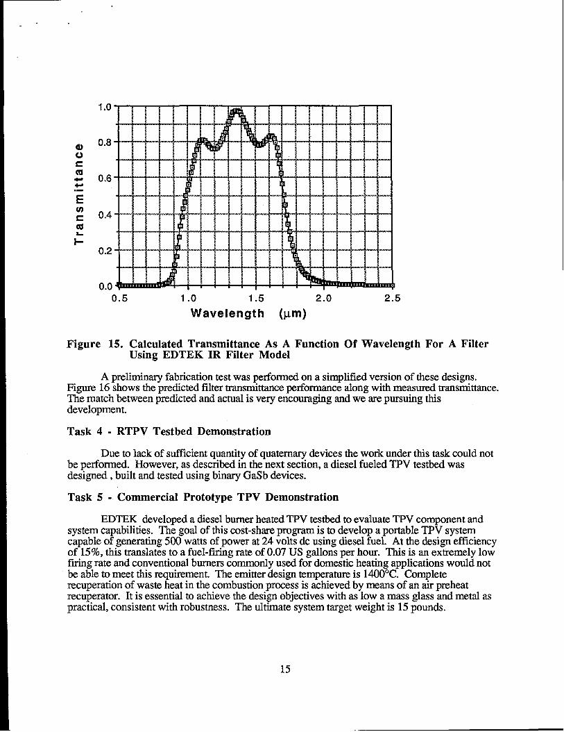
EDTEK is also developing a new design for terrestrial TPV considerations. Theperformance goals of this design are whole bandpass filters without the usual accompanying longtransmittance fail at wavelengths beyond the PV cell band edge. The potential of these designs isshown in figure 15 which is then predicted transmittance curve as calculated by our Ill filtercomputer model.
14
<
.“
1.0
0.8
0.6
0.4
0.2
0.00.5 1.0 1.5 2.0 2.5
Wavelength (~m)
Figure 15. Calculated Transmittance As A Function Of Wavelength For A FilterUsing EDTEK IR Filter Model
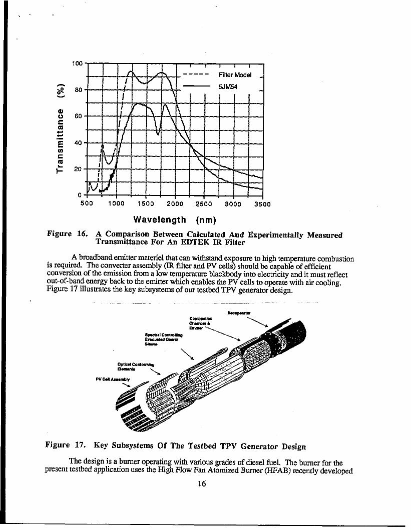
A preliminary fabrication test was performed on a simpliiled version of these designs.Figure 16 shows the predicted filter transmittance perfonmmce along with measured transmittance.The match between predicted and actual is very encouraging and we are pursuing thisdevelopment.
Task 4 - RTPV Testbed Demonstration
Due to lack of sufficient quantity of quaternary devices the work under this task could notbe performed. However, as described in the next section, a diesel fueled TPV testbed wasdesigned, built and tested using binary GaSb devices.
Task 5 - Commercial Prototype TPV Demonstration
EDTEK developed a diesel burner heated TPV testbed to evaluate TPV component andsystem capabilities. The goal of this cost-share program is to develop a portable TPVs ystemcapable of generating 500 watts of power at 24 volts dc using diesel fuel. At the design efficiencyof 15%, this translates to a fuel-firing rate of 0.07 US gallons per hour. This is an extremely lowftig rate and conventional burners commonly used for domestic heating applications would notbe able to meet this requirement. The emitter design temperature is 1400”C. Completerecuperation of waste heat in the combustion process is achieved by means of an air preheatrecuperator. It is essential to achieve the design objectives with as low a mass glass and metal aspractical, consistent with robustness. The ultimate system target weight is 15 pounds.
15
. .
100
80- — 5m5’4
60-
40-
I
o500 1000 1500 2000 2500 3000 3500
Wavelength (rim)
Figure 16. A Comparison Between Calculated And Experimentally MeasuredTransmittance For An EDTEK IR Filter
A broadband emitter materiel that can withstand exposure to high temperature combustionis required. The converter assembly (Et falter and PV cells) should be capable of efficientconversion of the emission from a low temperature blackbody into electricity and it must reflectout-of-band energy back to the emitter which enables the PV cells to operate with air cooling.Figure 17 illustrates the key subsystems of our testbed TPV generator design.
—- .—.——-—— _-—
Pv cdl
CombusilonCturrba& “k A“
-al -OlllngEvmcustadOianz \ Azi+zisbOv* A
\Optical COnlofmins AElomwm
\. -A
Figure 17. Key Subsystems Of The Testbed TPV Generator Design
The design is a burner operating with various grades of diesel fuel. The burner for thepresent testbed application uses the High FIow Fan Atomized Burner (HFAB) recendy developed
16
at Brookhaven National Laboratory (13NL)for low firing rates in heating applications. Lowpressure air is atomized through a patented nozzle. It was adapted for use in the TPV system inseveral ways. The inside components were modifkd to accommodate the extremely low ftig rateof 0.07 US gallons per hour required by the testbed design. As in the case of the HFAB, all the airused for atomization and combustion is introduced through the atomizer. The flow can becharacterized as a single central jet with a radial profile of axial velocity at the nozzle exit and aweak level of swirl (about 0.3 swirl number). In view of high flame temperatures and hightemperature of the atomizing air, it is necessary to incorporate novel features into the design toprevent the possibility of fuel coking. The fuel is injected towards the tip of the pre-filming surfaceto minimize the residence time on the hot surface.
The fuel line is cooled by circulating excess fuel near the injector tip. This cooling fuel isfrom the fuel system pressure regulator bypass and circulates in an outer jacket in the fuel lineassembly. Heat transferred into the circulating fuel (about 50 watts) is rejected to the air used toremove waste heat from the back of the cells. The swirler and the body of the atomizer are made ofInconel@alloy to withstand the high temperature environment. Parts that would come in contactwith the hot combustion gases are fabricated mostly from ceramic materials. The burner is ignitedby a pilot flame at starting, which in turn is lit by a hot surface type igniter, modified toaccommodate the piloting flow of fuel. The hot surface igniter/pilot flame approach was selectedover a spark system primarily due to weight considerations. The flame is ‘proved’ by athermocouple, whose output is integrated into the control system.
For this combustion and flame control there was concern that coke would form in thenozzle and be a problem. Testing has shown this not to be a problem and the nozzle componentsremain very clean in spite of the chamber environment and high temperature of the preheated air.
In the chamber defined by the emitter, the flame is contained within a flame tube. Both theemitter and the flame tube are made of sintered silicon carbide. The emitter is a cylinder, closed onone end. The flame tube is a cylinder with a small cast flange on one end. The hot gases exit theend of the flame tube, turn around and flow in the reverse direction within an annulus formed bythe flame tube and the emitter (fig. 17). The gases exit into the recuperator, which is essentiallymade up of three cylindrical annuli. The central annulus carries the hot combustion gas and theouter and inner annuli convey the air supply to the burner. Heat is transferred horn the hot gasesto preheat the incoming air to a design temperature of 1200°C. At the hot end of the recuperator,ceramic liner sleeves are used to reduce heat flux and keep the metal temperatures within acceptablelimits.
Thermal expansion is a significant design challenge in the sophisticated and highlyrecuperated combustion system. The emitter and recuperator/burner face components require theengineering of an interface to compensate for the different thermal expansion coefficients. At thesame time the system air pressure drop is fairly high – on the order of 8 inches of water. Of thispressure drop, roughly 2 inches are required for the recuperator and inlet/outlet pressure drops and6 inches are required for the atomizer. The seal between ceramic and metal components must bedesigned for the pressure drops imposed. For the testbed system developed here, layers of wovenceramic blankets were engineered to absorb differential expansion and maintain the air seal.
Task 6 - Results And Analysis Of Diesel Fueled TPV Testbed
The burner, the recuperator and the emitter were fabricate& assembled and tested toevaluate the thermal performance of thk system. Some of the results fi-oma test run of about twohours at the design fting rate of 0.07 US gallons per hour, are discussed below. Combustionperformance was evaluated by measuring the operating excess air level and by the levels of
.
emission of carbon monoxide and nitrogen oxides. Various gas and surface temperatures weremeasured to approximate the thermal performance.
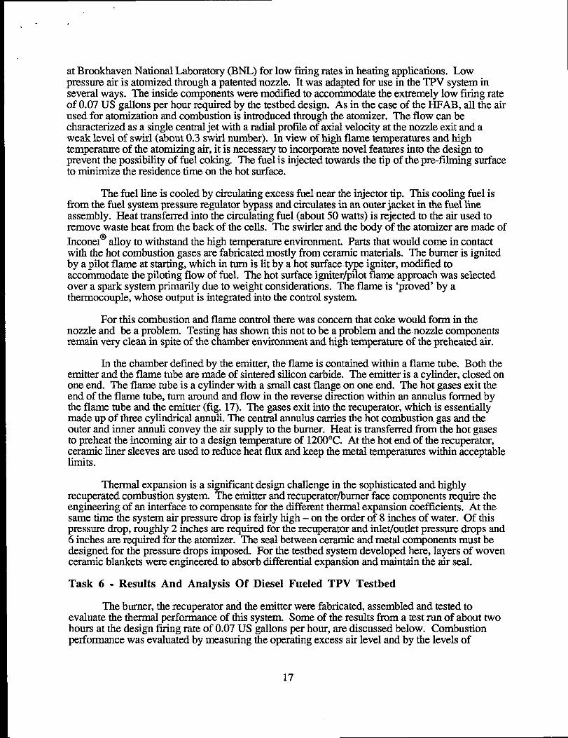
Figure 18 shows the constancy of fuel (power) input rate. The fuel supply system includeda pump, constant pressure regulator, and flow control orifice. During the test the flow rate wasmeasured by logging output signal tim a digital balance at 15-second intervals. The fluctuationswere due to the measurement procedure. Over each 15-second interval only 1 gram of fuel wasconsumed. It should be noted that, by design, there was a higher fuel flow rate at start up. Undercold conditions the air density at the end of the recuperator was higher, airflow through theatomizer was increased to provide about the same pressure drop during steady state. A lowatomizer pressure drop at startup would lead to poor atomization. To avoid very lean conditions atstint the fuel flow was increased to about three times the steady state level. A high startup firingrate resulted in improved ignition and faster system warm-up. As the system started up the densityof the gases through the system decreased and flow resistance increased which decreased airflowtoward the design specification. Fuel flow was decreased accordingly to maintain desired air/fuelratios. Fuel rate attributes were as expected.
02
0.1s
al
aw
o0
d.- d. t-”dm.a . lcn..nd-.l---- ~—- .. — ..”-,
40 60 80 140
Tilllafrumsu!t(uliu) “
a. Fuel (Power) Input vs. Time b. Combustion ChamberViewed Post Test
Figure 18. Burner Combustion Chamber Test Results
Figure 19 shows the variation in the temperature along the length of the emitter during asteady-state operation. The uniformity, a variation of about 20 degrees for an operatingtemperature of 1000°C, was quite good. The major reason for the lower temperature was omissionof the converter assembly to enable direct optical measurement of the emitter temperatures. Thepresence of such a fiiter/PV cell assembly would result in recycling out-of-band radiation resultingin a higher emitter temperature.
18
kfma4mml)aMltaraYIin&r(4
\
-loao 1020 1040 1060 10XO 1100
Emimtal~(c)
a. Emitter Temperature vs Length b.
Figure 19. Diesel Fueled TPV Emitter Test
Emitter Viewed Through ScreenDuring Burn Test.
Results
For the current natural gas burner in the current hybrid system, we propose to use the sameSiC material used in the diesel system which is designed to operate at 1400°C. The SiC material israted to operate to 1650°C and has been reported in the Iiterattue to survive to 1750°C. The maindifference in the emitter will be that the emitter cup will be scaled down to accommodate the 500electric output at a temperature of 1600°C. As already discussed in the sizing section, the emittercup will be 2.6 inches in diameter cylinder that is 3.1 inches long. Additionally, it will havewindows in the closed end to admit the concentrated solar energy. Figure 20 shows the basicconfiguration of the hybrid emitter cup.
/- ——.
Emitter
Figure 20. Preliminary Design Drawing For The Emitter Cup And CombustionChamber Area Of The Natural Gas Burner
Unlike the oil burner which used an Inconel metal bulkhead in the combustion chamber, aceramic such as zirconia or SiC (depending on relative costs) will be used for the hybrid systembulkhead due to the 1600°C operating temperature in the natural gas burner. Another difference in
19
the flame area of the natural gas burner design is that premixed natural gas and air cannot be used atthe level of preheat required for the incoming combustion air. On the other han& withoutpnmixing at cold startup the flame is unstable; therefore, we propose to supply premixed air andgas during start up that will be switched off after high temperature is reached. A double annulusconilgumtion is used in the combustion chamber as was shown in figure 18. The first smallanmdus provides shielding between the incoming air and the fuel nozzle while the second largerone, called the flame tube, is used to force the exhaust gases to flow outward along the inside ofthe emitter cup to achieve maximum heat transfer to the emitter.
The recuperator heat exchanger in the testbed oil burning system was made of Inconelmetal. Its design has been tested and proven sound. Figure 21 represents the combustion airpreheat temperature measured at the exit of the recuperator. Due to the excessive thermal mass ofthe thick wall heat exchanger, this testbed and the operating procedure combination took about 40minutes before steady-state was reached an~ again, the final temperature is lower than the designvalue because of the lower gas temperature at the combustion chamber exit. The recuperatoreffectiveness calculated from these measured data was 78% which exceeded the designperformance.
—. — ....
A....i. ,& .:. — *—. (f!)
aoo
m
4im
X@
o0 20 40 60 80 100 120 MU
Tiificasut(lnia)
a) Preheat Air Temperature vs Time b) Recuperator Viewed Post Test
Figure 21. Diesel Fueled TPV Recuperator Test Results
The combustion petiormance measurements made during steady state operation resulted inan excess air of 23%, 49 PPM for carbon monoxide, and 340 PPM for NOX. The NOX numberwas high compared to conventional oil burners because of high air preheating and resultant highpeak flame temperatures. The elevated emission numbers will improve during engineeringdevelopment and system integration.
Figure 22 illustrates the key features of the thermal containment vessel. The vessel consistsof two quartz flasks lwated concentrically so as to forma double walled container. The spacebetween the two walls is evacuated in order to limit heat transfer to the radiation mode whilesuppressing convective and conductive heat transfer. The section of the outer wall that is oppositeto the emitter, as shown by the shaded area in figure 22 has resonant mesh infrared filters bondedto the inside surface. The inside of the outer quartz wall. The inset graph in figure 22 illustratesthe function of the filters. The filters reflect most of the radiant energy spectrum back to the emitterwith >98% efficiency except for a band centered about the wavelengths that the GaSb PV cells canconvert most efficiently. The energy band about the resonant center fkquency is transmittedthrough the wall and eventually into the PV cells for conversion to electricity. The sections of thequartz wall not covered by filters are coated with a vapor deposited gold fti that reflects radiant
20
energy back into the vessel. In this way the unwanted radiative heat transfer across the system islimited to c2%. Thus the vessel effectively contains the thermal energy so that very little loss issustained through the walls.
GoldRaflaotorOn InaldaOf Outar A ‘-
InfraradFltmr On Quartz A
Inalda WWan
%? \/;
F=r$-
//
Innar Quartz ,=Wall
WCaaOrr
Vacuum
Outar GapBatwearr
1SM. F Tti&
Quart2Walls =0.4. , iOPv Odb
WallTr8wdlWW
Oz@ ,
n--0 1 2 a
wMklllth
~ Figure 22. Key Features Of The Thermal Containment Vessel And FunctionalDescription
Figure 23 shows the vessel prepared for testing. The thermal containment vessel wastested and found to work according to design in all respects except one. The filters were fabricatedonto thin, flat glass substrates and bonded to the curved inside surface of the vessel with a siliconebased adhesive. The adhesive system was tested in vacuum and found to resist temperatures inexcess of 250*C. Our thermal modeling indicated that the adhesive temperature would not exceed120*C in operation. The adhesive underneath the filter substrates did indeed survive the testingwith no degradation, however, the seams between the filter substrates allowed the adhesive in thecracks to be exposed to the full emitter radiant intensity. The adhesive in the seam degraded atemitter temperatures on the order of 1150*C. The adhesive then became the limiting factor in thedesign and limited our diesel fueled testbed evaluation to emitter temperatures below 1150”C.
Figure 24 illustrates the diesel fueled TPV converter assembly. The assembly consists offour arrays of GaSb PV cells. Each array is made up of 54 cells that are 1 cm x 1 cm square activearea. The cells in each 54-cell array are interconnected into nine strings that each contain six seriesconnected cells. The strings run ra&dly around the emitter to take ad;antage of the radialsymmetry of the radiation flux. Typical characteristics for the cells are also presented in the insetgraphs of figure 24. The converter assembly also consists of an array of prisms. The prismsoptically couple the PV cells to the outside of the quartz thermal containment vessel. The prismsare designed to intercept omni-directional blackbody radiation from the emitter and concentrate itonto the PV cells at the base of the prisms. The concentration is factor for the Prisms is desimedto be approximately 1.7 for the bla~kbody spectrum and was measured to be 1:7 during the &stbedevaluation thus, the prisms perform well according to design. Typical results are presented forsimilar prisms in figure 25 and the results of testing the converter are compared to theoreticalpredictions in figure 26. Basically, the converter worked according to design.
21
Figure 23. Thermal Containment Vessel Prepared For Testing
d I I0.0 0.1 0.2 0.3 0.4 OS
Volmw
-0.5
CURRENT-VOLTAGE RESPONSE
Figure 24. Diesel Fueled TPV Converter Assembly And Test
1.0 1.5 2.0
wm@en@h (PI
SPECTRAL RESPONSE
Results
22
0.70
0.60
0.50
z
:0.40
zalk 0.30
z
0.20
0.10
0.00
Wtih Prisms
0.00 0.20 0.40 0.60 0.80 1.00 1.20 1.40 1.60 1.8o
Voltage (Volta)
Figure 25. Measured Performance Of GaSb PV Cells With And WithoutConcentrating Prism
0.5
0.45- -
0.4- - Data from NREL Solar TPV demo*_e
1 0.35- -
$ 0.3- - Data from 500W Diesel Demo*
g(Multiple strings of six cell each)
0.25- -
h oz2.- -H
\*NOTE: B~fi demos ~~its ~ Simil
2 0.15- - PV cells, prisms,and filters. Emitter Single ceII/prisrr
w materialswere different and cavity ❑
o.1- - geometries were differenL❑
o.05- -Single Cell/prism
o500 600 700 800 900 1000 1100 1200 1300
Temperature (C)
Figure 26. Comparison Of Measured And Theoretical TPV Power Out VersusEmitter Temperature
23
.
.
Figure 27 illustrates the forced air heat exchanger that cools the PV cells in the converter.The heat exchanger consists of heat pipes that are bonded to the PV cell substrates and spread theheat ffom the cells over a length approximately twice the length of the cell array. The heat is thenconducted from this enlarged base into radial aluminum fms through which air is forced in order toextract and carry away the waste heat from the converter. The typical measured performance of theheat exchanger is presented in the inset graphs of figure 27. The converter thermal control systemeffectively maintains the PV cell temperature at or below 15°C above ambient air temperature.
..HEAT UCHMGES FERF~ ~ Vuuod HOrlzord
14~
G12.1
# 10v
●
$ :. TC2
i: ~
4
B’ ;.-.— -.. r.”.. - . . . . . -. - -- -. ----
6
0 200 400 ‘-- -’”
W CELL WASTE FOWE$
‘..=; . . . .mn .* nw. ma n nt m IW MiN
HeatPipes
Cooling-Fins
I bUU w
R (WattS)
Dwees FrorrrVwtlcel
2,:,.,. PV Cell Heat Exchanger Temperaturevs Generstor Operating Attitude
o
Figure 27. TPV Converter Thermal Control System And Test Results
In summary, a diesel fired TPV testbed has been design~ modele~ fabricat@ tested, andevaluated. The design has been confined by comparing the model predictions for the design withexperimentally measured performance values.
Task 7- Test Marketing And Pricing Study
The Charter Group, as a subcontractor, has performed marketing surveys on theapplication of TPV power sources to commercial and government markets. The surveys haveindicated that the cost of TPV systems is prohibitive for the commercial market- the cost beingprimarily determined by the TPV cells. The availability of lower cost quaternary PV cells wouldessentially generate a whole new market for the TPV power sources. Other factors which wouldbe mitigated downward are associated with quatemary cells requiring lower temperature operation,simplified cooling and less stringent materials problem.
A large market for small portable TPV power sources has been identifkd in the recreationvehicle @v) and boating industry for application to combined battery chargingJinverter powersources fueled either by diesel or propane energy sources. The RV industry is particularlysensitive to auxiliary generator noise and quietness of the TPV power source is particularlyappealing to that industry.
Another commercial application is emergency power for home heating oil/gas systems forcirculating forced hot air, hot water, or absorption type air conditioning when utility power has
24
.
. .c
.
failed. With the deregulation of the electric power industry and expected decrease in reliability andquality of power, the utilities are searching for methods to enhance their market appeal to keep theircurrent core of customers. ‘NW emergency power sources have been identified as an appealingoption that could be sold or leased to customers on a monthly charge basis.
An unexpected commercial market has been identified in computer laptop power sources.Battery solutions to-date has not measured up to the duration times needed for computing. This isafield application for essentially out-door industrial/commercial use. This market is very large.
Government markets have been identfled in small portable power sources for US Armyfield operations, where lightweight, portability and quietness of operation is of prime importance.The US Army, funded by DARPA, is now spending large R&D fimds to develop such a source.
In summary during this two year program we set up a THM crystal growth system to growGaInAsSb alloy single crystals. In spite of several growth optimization runs, we were unable togrow device quality quaternary crystals that were free of micro structural defects. In parallel, wetried to fabricate quaternary TPV devices using epitaxially grown quaternary layers. Theseattempts were not successful due to the inability of epi providers to supply device quality material.EDTEK designed IR fiiters were successfully optimized for the spectral response of the quaternarydevice. Optimized filters for space-based and terrestrial-based TPV applications weredemonstrated. A diesel fmd TPV testbed using II? filters and binary GaSb devices was set up andits performance characteristics were evaluated.
25
.r” -
.
Growth of GaInAsSbEpitaxial Layers and Junctions
Report for Tasks 1 and 2
Prepared for:
EDTEK, kC.
7082 S. 220th St.Kent, WA 98032
. Prepared by:
Dr. Paul R. SharpsResearch Triangle Institute
P. O. BOX12194Research Triangle Park, NC 27709-2194
July 29ti, 1997
.
The purpose of this report is to summarize work that was done by the ResearchTriangle Institute (RTI) during Tasks 1 and 2 in the development of GaInAsSb epitaxiallayers and junctions, for EDTEK, Inc. GaSb layers and junctions were to be initiallygrown, followed by the GaInAsSb layers and junctions. A total of 83 runs were madeusing two different organo-metallic vapor phase epitaxy (OMVPE) reactors during Tasks1 and 2. Of those runs, 76 were made for the growth of GaSb, and 7 were made for thegrowth of GaInAsSb. The growth of the GaSb and GaInAsSb material will be describedin the following paragraphs.
During the growth of the GaSb layers, a number of factors were’ found tosignificantly affect the material quaiity. These included the precursors, the VIDI ratio, thegrowth temperature, the substrate preparation, the substrate orientation, and the dopantchoice. All of those issues had to be addressed in order to obtain specular epitaxiallayers.
Initially, trimethyl gallium (TMGa) and tris(dimethylamino) antimony (TDMSb)were used as the Ga and Sb precursors. TMGa is a precursor that we have hadconsiderable experience with, and it was also already installed on the OMVPE reactors.TDMSb is a new Sb precursor being developed by Morton, and was used because itsupposedly was both easier to cr~k and also led to lower carbon incorporation into thefilms. Despite a number of growths under varying conditions, we were never able togrow specular epitaxial GaSb using TDMSb. The TDMSb was replaced with trimethylantimony (TMSb), which led to an immediate improvement in the quality of the epitaxiallayers. The difficulty with the TDMSb may be due to the low vapor pressure, and theinability to deliver sufficient precursor to the reactor chamber so that a suitable V/Ill ratiocan be achieved.
A second issue with the growth of GaSb is the V/111ratio. Variations of only 10%in the VLIIIratio can iead to a degradation in the film morphology. Because of the type ofprecursors involved (organometallics) it is necessmy to have a V/111ratio close to 1.Otherwise, the films are either Sb or Ga rich, and the surface morphology rapidlydeteriorates. Fortunately, we were able to characterize the films with EDAX (energydisperive analysis of X-rays) in an SEM (scanning electron microscope) to determine thecomposition. Using a GaSb wafer as a standard, it was relatively easy to determine if afilm is either Sb or Ga rich. The V/111ratio was modified for the next growth.
The third issue in the growth of the films was the growth temperature. Thegrowth temperature was varied between 475 “C and 600 ‘C, with the most specular fihnsin either reactor grown between 580 ‘C and 600 ‘C. The growth of the GaSb at lowertemperatures was of interest because the growth of GaInAsSb is thought to be better atlower temperatures. At higher growth temperatures GaInAsSb goes through a spinodaldecomposition due to a miscibility gap, and separates into two phases. However, forGaSb lowering the growth temperature below 575 “C in either reactor resulted in hazylooking films, i.e., films with considerable surface roughness.
.
●
The epitaxial films were grown on n-type and p-type GaSb substrates as well ason semi-insulating GaAs substrates. Semi-insulating GaSb substrates do not exist, so anyHall effect measurements have to be done on films either grown on semi-insulating GaAsor on GaSb substrates of the opposite polarity. Also, film thicknesses were measuredwith an SEM. In order to have a contrast between the epitaxial film and the substrate, anyfilms used for thickness measurements had to be grown on the semi-insulating GaAssubstrates.
A number of suitable etches exist for the preparation of GaAs substrates forepitaxial growth. We typically do an ultrasonic solvent clean in trichloroethylene,acetone, and methanol, followed by an ethc in 2:1:10 ammonium hydroxide: hydrogenperoxide:D.I. water. Preparation of GaSb substrates, however, is more challenging. It isdifficult to completely remove the oxides from the surface. Initially, we used the sameetch as that used for the preparation of GaAs. Eventually, the hydrogen peroxide wasremoved from the etch. While specular films were grown using both etches, deviceresults from the epitaxial junctions led us to believe that the oxides were not totallyremoved from the surface. During the final growths (final 27 runs) a 1:1 hydrochloricacid:D.I. water etch was used. The GaSb substrates were solvent cleaned, dipped in theetch for 30 seconds, blown dry, and finally loaded in the reactor.
One idea considered to remove the oxides on the GaSb was a 650 “C bake-outwith an AsH3 overpressure. It was thought that the AsH3 would decompose, with theresulting hydrogen radicals removing any oxides and the remaining As passivating thesurface. However, all of the films grown with the AsH3 overpressure were very hazy. Assoon as the AsH3 high temperature step was removed, the surface of the films improved.It is believed that the surface of the GaSb decomposes at the higher temperature, and thatthe As on the surface causes the ensuing poor morphology. A lower temperature bake-out with the AsH3 might not lead to the surface degradation, and might also remove theoxide. Insufficient resorces and time prevented this option from being pursued.
Layers were grown on both (100) and 2° off (100) toward <110> GaSb wafers.None of the films grown on the (100) wafers were specular, despite using the samegrowth conditions that gave specular layers on the 2° off substrates. The steps and ledges.on the surface of the 2° off substrates are necessary for good 2-dimensional growth tooccur. The poor morphology of a number of growths was attributed to the on-axissubstrates.
Considerable effort was made to dope and calibrate both n-type and p-type films.As mentioned before, Hall effect measurements were used to determine the carrierdensity. The Hall effect measurements were made on both semi-insulating GaAssubstrates as well as on GaSb substrates of a polarity opposite to what the film wasthought to be. The difficulty is that the films grown on the GaAs substrates were oftenhazy, and while the carrier density measurements were thought to be accurate, themobility numbers were not considered too reliable due to scattering from defects, etc.Care must also be taken with the Hall effect measurements made on the layers grown on
2
GaSb because of current leakage through the junction, i.e., the epitaxial layer may not beelectrically isolated from the substrate. Also, depletion in the epitaxial layer may reducethe effective film thickness for layers with a lower carrier density. A few samples weremeasured with a capacitance-voltage profiler, but in general the leakage currents were toohigh for a good Schottky barrier to be made to the material.
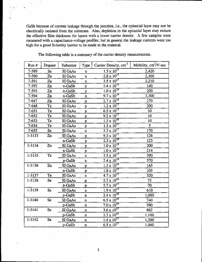
The following table is a summary of the carrier density measurements.
Run # Dopant Substrate Type Carrier Density, cm”3 Mobility, cm2/V-sec
7-589 Se S1GaAs n 1.5 x 10¹⁷ 2,420~ 7-590 Zn 2.8 X 10’ 2,360
7-591 Zn S1Gtis n 3.5 x 10’7 2,2107-592 Zn n-GaSb P 5.4 x 10¹⁹ 1407-593 Zn n-GaSb P 1.0 x 10’9 2007-594 Zn n-GaSb n 9.7 x 10¹⁹ 3,3007-647 Zn S1GaAs P 2.7 X 10¹⁸ 2707-648 Te S1GaAs P 1.2 x 10’7 2007-651 Te S1GaAs P 6.5 X 10¹⁷ 107-652 Te S1GaAs P 9.2 X 10¹⁷ 107-653 Te S1GaAs P 1.3 x 10’8 107-654 Te S1GaAs P 1.3 x 10’7 57-655 Se S1GUS n 3.3 x 10¹⁷ 170
-1-3133 Zn S1GaAs P 9.3 x 10¹⁷ 126n-GaSb P 2.3 X 10i9 123
1-3134 Zn S1GaAs P 1.0 x 10¹⁸ 200n-GaSb P 1.0 x 10’9 214
1-3135. Te S1GaAs n 3.5 x 10¹⁷ 390p-GaSb n 2.4 X 10¹⁸ 570
1-3136 Zn S1G*s P 1.3 x 10¹⁹ 165n-GaSb P 1.8 x 10’9 105
1-3137 Te S1GaAs n 4.7 x 10¹⁷ 3201-3138 Se S1GaAs P 5.7 x 10’6 75
p-GaSb P 5.7 x 10’7 701-3139 Se S1GaAs n 1.9 x 10’7 610
p-GaSb n 2.4 X 10¹⁸ 1,0001-3140 Se S1GaAs n 6.5 X 10IG 740
p-GaSb n 7.0 x 10¹⁹ 5901-3141 Se S1GaAs n 3.6 X 10¹⁷ 862
p-GaSb n 3.3 x 10¹⁸ 1,1601-3142 Se S1GaAs n 1.4 x 10¹⁷ 1,200
p-GaSb n 6.5 X 10¹⁷ 1,060 J
3
As can be seen from the data in the table, there is considerable variation in theresults from the Hall effect measurements, depending on the type of substrate used. Halleffect measurements were considered reliable if the results from the films grown on theGaAs and the GaSb substrates were similar to each other. This is not easy to. achieve.Run 1-3136 gave consistent results, but unfortunately the carrier density is in the 1 x 1019cm-3 range. Run 1-3142 gave the most consistent results for the n-type doping, but evenhere the results from the different substrates varied by a factor of 5.
Both Se and Te were considered for the n-type dopant. Se gave the best results,but part of this may be due to the Te precursor, di-isopropyl telluride (DIPTe). In usingDIPTe, we generally did not type convert the materkd to n-type. The Se source, hydrogenselenide (H2Se), gave much better contol over the n-type doping.
Several GaSb epitaxial layers and p-on-n junctions were sent to EDTEK forprocessing. The device results indicates difficulties in two areas. First, there appeared tobe a blocking layer in the devices, possibly from the oxide layer not being removed fromthe substrate. Secondly, the minority carrier lifetime in the n-type layers is very poor,possible due to compensation. The quality of the GaSb material must be improved, and abetter substrate preparation technique has to be found.
Seven (7) runs were made in an attempt to grow the GaInAsSb. All of theepitaxial layers were very hazy. None of the samples were lattice-matched to the GaSbsubstrates, as measured by a single crystal X-ray diffractometer. Because GaInAsSb is aquatemary, both the lattice constant and the band gap are necessary to determine the filmcomposition. The material was not specular enough for transmission measurements togive meaningful results, and we do not have a PL system that can measure a signal below0.73 eV.
In summary, more work is needed with the GaSb. While specular GaSb can begrown, the electrical properties of the material appears to be poor. n-type epitaxial GaSbhas to be grown with a good minority carrier lifetime before good junctions can be made.The substrate preparation technique also has to be improved, to ensure that the oxide onthe GaSb is removed. While progress was made in growing the GaSb, more workremains before work should commence on growing the GaInAsSb.
‘At the end of June, $17,996.81 had been spent on the contract, with another$1,493.50 in commitments. More effort was expended during the month of July, which isnot included in these numbers. Work will not continue on the contract until directed todo SO by EDTEK, kC.
4