Embed Size (px)
Citation preview

SERVICE MENUAL
FOR L1510A
TFT-LCD TV
Haier Group

Content CONTENTS -----------------------------------------------------------------------------------------------1 Main Unit Description----------------------------------------------------------------------------------2 Features----------------------------------------------------------------------------------------------------4 Warning and Cautions---------------------------------------------------------------------------------6 Replacement of Memory IC--------------------------------------------------------------------------8 Net Dimension-------------------------------------------------------------------------------------------9 Remote Controller Functions----------------------------------------------------------------------10 ICs function description ----------------------------------------------------------------------------13 Block Diagram------------------------------------------------------------------------------------------21 Trouble Shooting---------------------------------------------------------------------------------------26

Front Panel Controls
Control Panel Function
6 7
TV/AV MENU VOL- VOL+ CH- CH+ POWER
2 3 4 5
1. Power supply switch2.TV/AV PC/COMPONENT/AV/SV/TV3. MENU Press to select the main menu4. VOL- Volume down / Left orientation to adjust the item in the OSD VOL+ Volume up / Right orientation to adjust the item/Press to enter 5. CH- TV channel down / to select the item in the menu CH+ TV channel up / to select the item in the menu6. Power indicator Illuminates red in standby mode, illuminates green when the display is turned on7.Remote Sensor
Selects the input signals:
Receives the signals from the remote control
/blue
1
4
5
4
2 3
16 7
5
L1510A
L2310A
6
7
L1910A

AV /S-VIDEO/COMPONENT Audio InputConnect audiooutput from an external device to this jack
VGA Input
Connect to the VGA 15PIN analog outputconnector of the PCdisplay card for PC display purpose
S-Video InputConnect S-Video outfrom an S-Video deviceto the jacks.
Antenna InputConnect cable or antenna signals to the TV, either direc-tly or through your cable box.
Connection Options
Earphone port
PC Audio InputConnect the PC outputconnector from a PC tothe audio input port
The figure is just for reference, please see the actual unit. )
L1510A/L1910A
DVD/DTV Input Connect a component video/audiodevice to these jacks
ANT IN S-VIDEO VGA INPC AUDIO IN AUDIO IN
R L
VIDEO IN
V
PbPr Y
COMPONENT IN
AN
T IN
S-V
IDE
OV
GA
INP
C A
UD
IO IN
AU
DIO
IN
RL
VID
EO
IN
V
Pb
Pr
Y
CO
MP
ON
EN
T IN
Video InputConnect videooutput from an external device to this jack
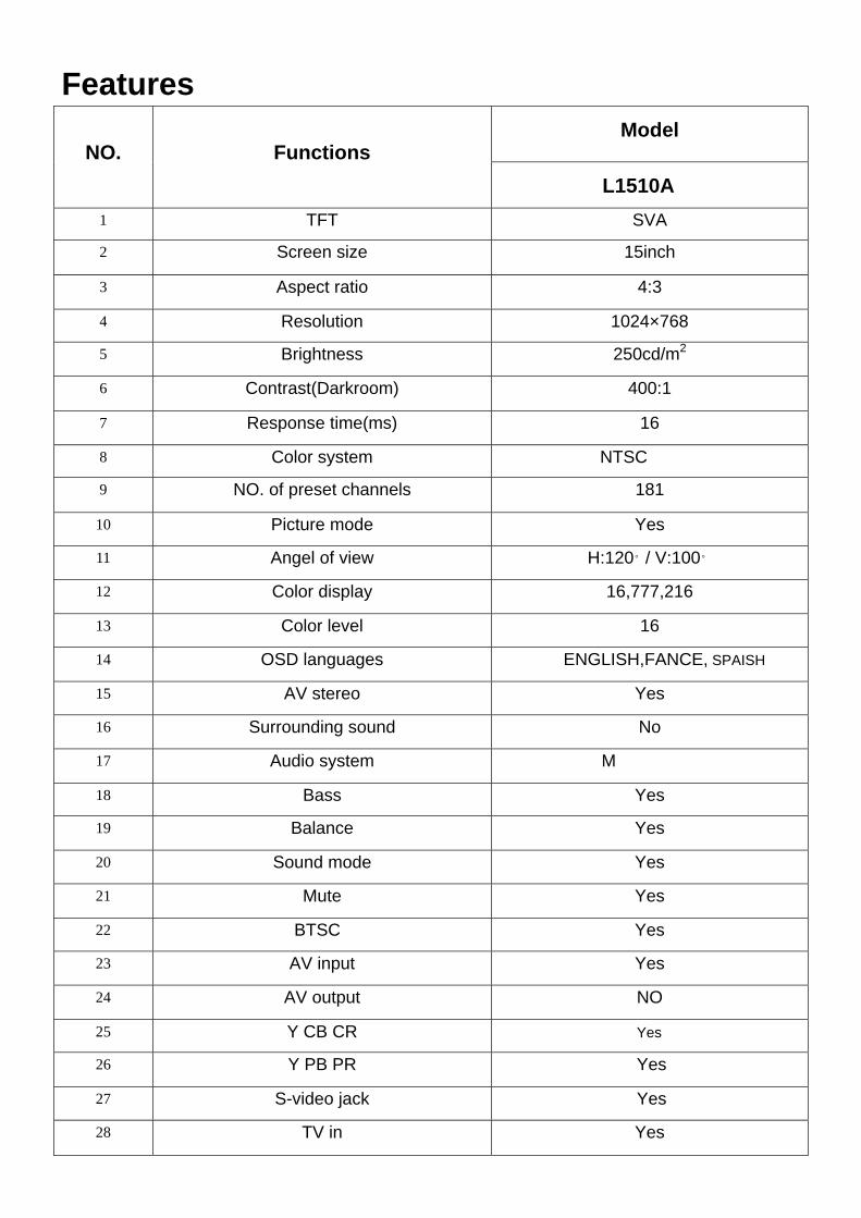
Features Model
NO.
Functions L1510A
1 TFT SVA
2 Screen size 15inch
3 Aspect ratio 4:3
4 Resolution 1024×768
5 Brightness 250cd/m2
6 Contrast(Darkroom) 400:1
7 Response time(ms) 16
8 Color system NTSC
9 NO. of preset channels 181
10 Picture mode Yes
11 Angel of view H:120°/ V:100°
12 Color display 16,777,216
13 Color level 16
14 OSD languages ENGLISH,FANCE, SPAISH
15 AV stereo Yes
16 Surrounding sound No
17 Audio system M
18 Bass Yes
19 Balance Yes
20 Sound mode Yes
21 Mute Yes
22 BTSC Yes
23 AV input Yes
24 AV output NO
25 Y CB CR Yes
26 Y PB PR Yes
27 S-video jack Yes
28 TV in Yes

Model
NO.
Functions
L1510A
29
D-SUB jack Yes
30 DVI socket
NO
31 SCART socket
NO
32 Ear-Phone Out
Yes
33 CCD,V-CHIP
Yes
34 Semitransparent menu
Yes
35 ZOOM
NO
36 16:9 mode
NO
37 Child Lock
YES
38 Quick View
Yes
39 NO. of built-in speakers
2
40 Audio output power(Built-in)(W)
2*1.5
41 Total power input(W)
40
42 Voltage range(V)
120
43 Power frequency(Hz)
60
44 Time of sleep timer(MINS)
240
45 Approval
UL
46 Suitable market
U.S.

Warnings and Cautions
Warning High voltages are used in the operation of this product.
Do not romove the cabinet back from your set. Refer
servicing to qualified service personnel.
Warning
To prevent fire or electrical shock hazard, Do not expose
the main unit to rain or moisture.
Warning Do not drop or push objects into the television cabinet
slots or openings. Never spill any kind of liquid on the
television receiver.
Caution
If the television is to be built into a
compartment or similarly enclosed, the
minimum distances must be maintained.
Heat build-up can reduce the service life of
your television, and can also be dangerous.
!Minimum 10c
20c
10c 5cm

Caution Never stand on, lean on, push suddenly the product or its
stand. You should pay special attention to children to children.
Caution
Do not place the main unit on an unstable cart stand, shelf or
table. Serious injury to an individual, and damage to the
television, may result if it should fall.
Caution When the product is not used for an extended period of time, it
is advisable to disconnect the AC power cord from the AC
outlet.
Caution
Avoid exposing the main unit to direct sunlight and other
source of the heat. Do not stand the television receiver
directly on other produces which give off heat. E. g. video
cassette players,Audio amplifiers. Do not block the
ventilation holes in the back cover. Ventilation is essential to
prevent failure of electrical component. Do not squash power
supply cord under the main unit.
Caution
The LCD panel used in this product is made of glass.
Therefore, it can break when the product is dropped or
applied with impact. Be careful not to be injured by
broken glass pieces in case the LCD panel breaks.
!
!
!
!
!

REPLACEMENT OF MEMORY IC 1. MEMORY IC This LCD TV uses memory IC. In the memory IC are memorized data for correctly operating the video and
sound circuits. When replacing memory IC, be sure to use IC written with the initial value of data.
2.CHECK MEMORY IC
(1) Power off Unplug the ~120V power plug from ~120V power socket. (2) Replace IC Be sure to use memory IC written with the initial data values or blank memory IC. (3) Power On Plug the ~120V power plug into ~120V power socket. (If memory IC is blank, the program will take 25s to
initial memory IC. (4) Check and set SYSTEM default value:
1) Press “DISPLAY” key, then press colour key “red”,”green”,yellow”,”DISPLAY” on the Remote control
unit continuously for factory used.
2) The “Factory2” will be displayed on the screen,
3) Check the setting value of the SYSTEM default value of Table below. If the vale is different, select
items by [CH-]&[CH+] keys and set value by [VOL-]&[VOL+] keys.
4) Press “OK” key and return to the normal screen.

Remote Control Key FunctionsWhen using the remote control, aim it towards the remote sensor on the TV
2. Power supply switch
9. MENU To display/exit the main menu
11. CH+/CH- TV channel up/down or select the item of the menu
12. VOL+ Volume up / to select the main menu/ to adjust the item/ toenter the submenu.
VOL- Volume down / to select the main menu/ to adjust the item
6. 0-9 TV channel number select
3. RECALL Quick TV channel switch(return to the last channel)
10. TV/AV Select PC/COMPONENT/AV/SV/TV
7. MTS/SAP Select MONO,STEREO, SAP in NTSC system
1. MUTE MUTE
8. P.STD Select picture mode: PERSONAL/STANDARD/MILD/FRESH
5. DISPLAY Display current input signal information
4. EXIT Menu exit
Illustration of the keys on the remote control:
MUTE
RECALL DISPLAY EXIT
1 2 3
4 5 6
7 8 9MTS/SAP P.STD
MENU TV/AV
CH+
CH-
VOL -
VOL +
CCD SLEEP SCAN
0
1 2
3 45
6
7 8
9 1011
12
13 1415
13. CCD Closed caption on/off
14. SCAN Channel scan
15. SLEEP TV sleep button

Remote Control
Installing Batteries
1.Slide open the cover of the battery compartment on the back of the remote control.2.Load two batteries in the compartment. (plus and minus poles to respective mark)3.Replace the cover of the battery compartment.
AAA alkaline
+
-

ICs Function Description 1.UOC3 Function:TV signal processor with Teletext and Nicam
PIN SYMBOL DESCRIPTION 1 VSSP2 ground 2 VSSC4 ground 3 VDDC4 Digital supply to SDACs(1.8V) 4 VDDA3(3.3V) Supply(3.3V) 5 VREF_POS_LSL Positive reference voltage SDAC(3.3V) 6 VREF_NEG_LSL+HPL Negative reference voltage SDAC(0V) 7 VREF_POS_LSR+HPR Positive reference voltage SDAC(3.3V) 8 VREF_NEG_HPL+HRP Negative reference voltage SDAC(0V) 9 VREF_POS_HPR Positive reference voltage SDAC(3.3V) 10 XTALIN Crystal oscillator input 11 XTALOUT Crystal oscillator output 12 VSSA1 ground
13 VGUARD/SWIO V-guard input/I/O switch (e.g.4mA current sinking capability for direct drive of LEDs)
14 DECDIG Decoupling digital supply 15 VP1 1st supply voltage TV-processor(+5V) 16 PH2LF Phase-2 filter 17 PH1LF Phase-1 filter 18 GND1 Ground 1 for TV-processor 19 SECPLL SECAM OLL decoupling 20 DECBG Bandgap decoupling 21 EWD/AVL East-West drive output or AVL capacitor 22 VDRB Vertical drive B output 23 VDRA Vertical drive A output 24 VIFIN1 IF input 1 25 VIFIN2 IF input 2 26 VSC Vertical sawtooth capacitor 27 IREF Reference current input 28 GNDIF Ground connection for IF amplifier 29 SIFN1/DVBIN1 SIF input 1/ DVB input 1 30 SIFN2/DVBIN2 SIF input 2/ DVB input2 31 AGCOUT Tuner AGC output 32 EHTO EHT/over voltage protection input
33 AVL/SWO/SSIF/REFO/REFIN
Automatic volume leveling/switch output/sound IF input sub-carrier reference output/external reference signal mixer for DVB operation

34 AUDIOIN5L Audio-5 input(left signal) 35 AUDIOIN5R Audio-5 input(right signal) 36 AUDOUTSL Audio output for SCART/CINCH(left signal) 37 ADUOUTSR Audio output for SCART/CINCH(right signal) 38 DECSDEM Decoupling sound demodulator
39 QSS0/AMOUT/AUDEEM
QSS inter-carrier output/AM output/deemphasis(front-end audio out)
40 GND2 Ground 2 for TV processor 41 PLLIF IF-PLL loop filter
42 SIFAGC/DVBAGC AGC sound IF/internal-external AGC for DVB applications
43 DVBO/IFVO/FMRO Digital Video Broadcast output/IF video output/FM radio output
44 DVBO/FMRO Digital Video Broadcast output/IF video output 45 VCC8V 8 Volt supply for audio switches 46 AGC2SIF AGC capacitor second sound IF 47 VP2 2th supply voltage TV processor(+5V) 48 IFVO/SVO/CVBSI IF video output/selected CVBS out/CVBS input 49 AUDIOIN4L Audio-4 input(left signal) 50 AUDIOIN4R Audio-4 input(right signal) 51 CVBS4/Y4 CVBS4/Y4 input 52 C4 Chroma-4 input 53 AUDIOIN2L/SSIF Audio 2 input (left signal)/sound IF input 54 AUDIOIN2R Audio 2 input (right signal) 55 CVBS2/Y2 CVBS2/Y2 input 56 AUDIOIN3L Audio 3 input(left signal) 57 AUDIOIN3R Audio 3 input(right signal) 58 CVBS3/Y3 CVBS 3/Y2 input 59 C2/C3 Chroma-2/3 input 60 AUDOUTLSL Audio output for audio power amplifier (left signal) 61 AUDOUTLSR Audio output for audio power amplifier (right signal) 62 AUDOUTHPL Audio output for headphone channel (left signal) 63 AUDOUTHPR Audio output for headphone channel (right signal) 64 CVBSO/PIP CVBS/PIP output 65 SVM Scan velocity modulation output
66 FBISO/CSY Flyback input/sandcastle output or composite H/V timing output
67 HOUT Horizontal output 68 VSScomb Ground connection for comb filter 69 VDDcomb Supply voltage for comb filter(5V)
70 VIN(R/Prin2/Cx) V-input for YUV interface(2th 日 input/Pr input or Cx input)
71 UIN(B/PBIN2) U-input for YUV interface(2th B input/PB input)

72 YIN(G/YIN2/CVBS-Yx)
Y-input for YUV interface(2th G input/Y input or CVBS/Yx input)
73 YSYNC Y-input for sync separator 74 YOUT Y-output (for YUV interface)
75 UOUT(INSSW2) U-output for YUV interface(2nd RGB/YPbPr insertion input)
76 VOUT(SWO1) V-output for YUV interface(general purpose switch output)
77 INSSW3 3rd RGB/YPbPr insertion input 78 R/PRIN3 3rd R input/Pr input 79 G/YIN3 3rd G input/Y input 80 B/PbIN3 3rd B input/P5 input 81 GND3 Ground 3 for TV-processor 82 VP3 3rd supply for TV processor 83 BCLIN Beam current limiter input 84 BLKIN Black current input 85 RO Red output 86 GO Green output 87 BO Blue output
88 VDDA1 Analog supply for TCG u-Controller and digital supply for TV-processor(+3.3V)
89 VREFAD_NEG Negative reference voltage (0V) 90 VREFAD_POS Positive reference voltage (3.3V) 91 VREFAD Reference voltage for audio ADCs(3.3/2V) 92 GNDA Ground 93 VDDA(1.8V) Analogue supply for audio ADCs(1.8v) 94 VDDA2(3.3V) Supply voltage SDAC(3.3V) 95 VSSadc Ground for video ADC and PLL 96 VDDadc(1.8V) Supply voltage video ADC and PLL
97 INTO/P0.5 External interrupt 0 or port 0.5(4mA current sinking capability for direct drive of LEDs)
98 P1.0/INT1 Port 1.0 or external interrruput1 99 P1.1/T0 Port 1.1 or Counter/Timer 0 input 100 VDDC2 Digital supply to core(1.8V) 101 VSSC2 ground 102 P0.4/I2SWS Port 0.4 or I2S word select 103 P0.3/I2SCLK Port 0.3 or I2S clock 104 P0.2/I2SDO2 Port 0.2 or I2S digital output 2 105 P0.1/I2SDO1 Port 0.1 or I2S digital output 1 106 P0.0/I2SD1I/O Port 0.0 or I2S digital input 1 or I2S digital output 107 P1.3/T1 Port 1.3 or Counter/Timer 1 input 108 P1.6/SCL Poet 1.6 or I2C-bus clock line 109 P1.7/SDA Port 1.7 or I2C-bus data line

110 VDDP(3.3V) Supply to periphery and on-chip voltage regulator(3.3V)
111 P2.0/TPWM Poet 2.0 or tuning PWM output 112 P2.1/PWM0 Port 2.1 or PWM0 output 113 P2.2/PWM1 Port 2.2 or PWM1 output 114 P2.3/PEM2 Port 2.3 or PWM2 output 115 P3.0/ADC0 Port 3.0 or ADC0 input 116 P3.1/ADC1 Port 3.1 or ADC1 input 117 VDDC1 Digital supply to core(+1.8) 118 DECV1V8 Decoupling 1.8V supply 119 P3.2/ADC2 Port 3.2 or ADC2 input 120 P3.3/ADC3 Port 3.3 or ADC3 input 121 VSSC/P Digital ground for u-Controller core and periphery 122 P2.4/PWM3 Port 2.4 or PWM3 output 123 P2.5/PWM4 Port 2.5 or PWM4 output 124 VDDC3 Digital supply to core(1.8v) 125 VSSC3 ground 126 P1.2/INT2 Port 1.2 or external interrupt 2 127 P1.4/RX Port 1.4 or UART bus 128 P1.5TX Port 1.5 or UART bus
2.RTD2023B PIN SYMBOL DESCRIPTION
1 APLL_GND Ground for multi-phase PLL 2 APLL_VDD Power for multi-phase PLL 3 PLL_TEST1 Test Pin 1 Power-on-latch for MCU crystal location 4 PLL_TEST2 Test Pin 2 Power-on-latch for crystal in frequency 5 TMDS_TST TMDS_TEST Pin Power-on-latch for host interface type 6 REXT Impedance Match Reference. 7 TMDS_VDD TMDS power 8 RX2P Differential Data Input 9 RX2N Differential Data Input 10 TMDS_GND TMDS ground 11 RX1P Differential Data Input 12 RX1N Differential Data Input 13 TMDS_VDD TMDS power 14 RX0P Differential Data Input 15 RX0N Differential Data Input 16 TMDS_GND TMDS ground 17 RXCP Differential Data Input 18 RXCN Differential Data Input 19 AVS0 ADC vertical sync input 5V tolerance Power from PIN

13 20 AHS0 ADC horizontal sync input Adjustable Schmidt trigger
5V tolerance Power from PIN 13 21 ADC_VDD ADC Power 22 ADC_GND ADC Ground 23 B0+ 1st Positive BLUE analog input (Pb+) 24 B0 1st Negative BLUE analog input (Pb-) 25 SOG0 1st Sync on Green 26 G0+ 1st Positive GREEN analog input (Y+) 27 G0 1st Negative GREEN analog input (Y-) 28 R0+ 1st Positive RED analog input (Pr+) 29 R0 1st Negative RED analog input (Pr-) 30 V7 Video8 bit 7 31 V6 Video8 bit 6 32 V5 Video8 bit 5 33 V4 Video8 bit 4 34 V3 Video8 bit 3 35 V2 Video8 bit 2 36 V1 Video8 bit 1 37 ADC_GND ADC Ground 38 ADC_VDD ADC Power 39 V0 Video8 bit 0 40 VCLK Video8 Clock 41 NC -- 42 NC -- 43 NC -- 44 NC -- 45 NC -- 46 Digital 1.8V Ground GNDK 47 Digital 1.8V Power VCCK 48 COUT Crystal out 49 PWM2 Pulse width modulation output port2 50 DDCSCL1(ADC) Open drain (Internal 75K pull high) 51 DDCSDA1(ADC) Open drain (Internal 75K pull high) 52 DCLK CLOCK 53 DENA DATA ENABLE 54 BGRN0 Display B-port Green Data 0 55 BGRN1 Display B-port Green Data 1 56 BRED0 Display B-port Red Data 0 57 BRED1 Display B-port Red Data 1 58 BJT_B Embedded regulator P type BJT control pin out 59 Pad 3.3V Power PVCC 60 Pad 3.3V Ground PGND

61 BBLU7 Display B-port Blue Data 7 62 BBLU6 Display B-port Blue Data 6 63 BBLU5 Display B-port Blue Data 5 64 BBLU4 Display B-port Blue Data 4 65 BBLU3 Display B-port Blue Data 3 66 BBLU2 Display B-port Blue Data 2 67 BBLU1 Display B-port Blue Data 1 68 BBLU0 Display B-port Blue Data 0 69 BGRN7 Display B-port Green Data 7 70 BGRN6 Display B-port Green Data 6 71 NC -- 72 NC -- 73 BGRN5 Display B-port Green Data 5 74 BGRN4 Display B-port Green Data 4 75 BGRN3 Display B-port Green Data 3 76 BGRN2 Display B-port Green Data 2 77 BRED7 Display B-port Red Data 7 78 BRED6 Display B-port Red Data 6 79 BRED5 Display B-port Red Data 5 80 BRED4 Display B-port Red Data 4 81 BRED3 Display B-port Red Data 3 82 BRED2 Display B-port Red Data 2 83 Pad 3.3V Power PVCC 84 Pad 3.3V Ground PGND 85 ABLU7 Display A-port Blue Data 7 86 ABLU6 Display A-port Blue Data 6 87 ABLU5 Display A-port Blue Data 5 88 ABLU4 Display A-port Blue Data 4 89 ABLU3 Display A-port Blue Data 3 90 ABLU2 Display A-port Blue Data 2 91 ABLU1 Display A-port Blue Data 1 92 ABLU0 Display A-port Blue Data 0 93 AGRN7 Display A-port Green Data 7 94 AGRN6 Display A-port Green Data 6 95 NC -- 96 NC -- 97 AGRN5 Display A-port Green Data 5 98 AGRN4 Display A-port Green Data 4 99 AGRN3 Display A-port Green Data 3 100 AGRN2 Display A-port Green Data 2 101 ARED7 Display A-port Red Data 7 102 ARED6 Display A-port Red Data 6 103 ARED5 Display A-port Red Data 5

104 ARED4 Display A-port Red Data 4 105 ARED3 Display A-port Red Data 3 106 ARED2 Display A-port Red Data 2 107 Pad 3.3V Ground PGND 108 Pad 3.3V Power PVCC 109 33VPNLOUT Panel on/off switch ot(Max current driving 1A) 110 COUT Crystal out 111 ARED1 Display A-port Red Data 1 112 ARED0 Display A-port Red Data 0 113 AGRN1 Display A-port Green Data 1 114 AGRN0 Display A-port Green Data 0 115 SDIO[3] Serial control I/F data in or Parallel port data [3] (Open
drain) MSB 116 Digital 1.8V Power VCCK 117 Digital 1.8V Ground GNDK 118 SCSB Serial control I/F chip select (Open drain) 119 SCLK Serial control I/F clock (Open drain) 120 DDCSDA2(DVI) Open drain (Internal 75K pull high) 121 DDCSCL2(DVI) Open drain (Internal 75K pull high) 122 PWM0 Pulse width modulation output port0 123 RESET_OUT Reset out 124 33VRST_REF Reference 3.3v for Reset Out 125 DPLL_VDD Power for digital PLL 126 DPLL_GND Ground for display digital PLL 127 XO Crystal OSC output 128 XI Reference clock input from external crystal or from
single-ended CMOS/TTL OSC
3.SM5964(PLCC) Function: MCU PIN SYMBOL DESCRIPTION
1 P4.2 Bit 2 of port 4
2 P1.0/T2 Bit 0 of port 1 & timer 2 clock out
3 P1.1/T2EX Bit 1 of port 1 & timer 2 control
4 P1.2 Bit 2 of port
5 P1.3/SPWM0 Bit 3 of port 1 & SPWM Channel 0
6 P1.4/SPWM1 Bit 4 of port 1 & SPWM Channel 1
7 P1.5/SPWM2 Bit 5 of port 1 & SPWM Channel 2
8 P1.6/SPEM3 Bit 6 of port 1 & SPWM Channel 3
9 P1.7/SPEM4 Bit 7 of port 1 & SPWM Channel 4
10 RES Reset
11 P3.0/RXD Bit 0 of port 3 & Receive data

12 P4.3 Bit 3 of port 4
13 P3.1/TXD Bit 1 of port 3 & Transmit data
14 P3.2/INT0 Bit 2 of port 3 & low true interrupt 0
15 P3.3/INT1 Bit 3 of port 3 & low true interrupt 1
16 P3.4/T0 Bit 4 of port 3 & Timer 0
17 P3.5/T1 Bit 5 of port 3 & Timer 1
18 P3.6/WR Bit 6 of port 3 & ext. memory write
19 P3.7/RD Bit 6 of port 3 & ext. memory read
20 XTAL2 Crystal out
21 XTAL1 Crystal in
22 VSS Sink voltage, ground
23 P4.0 Bit 0 of port 4
24 P2.0/A8 Bit 0 of port 2 & bit 8 of external memory address
25 P2.1/A9 Bit 1 of port 2 & bit 9 of external memory address
26 P2.2/A10 Bit 2 of port 2 & bit 10 of external memory address
27 P2.3/A11 Bit 3 of port 2 & bit 11 of external memory address
28 P2.4/A12 Bit 4 of port 2 & bit 12 of external memory address
29 P2.5/A13 Bit 5 of port 2 & bit 13 of external memory address
30 P2.6/A14 Bit 6 of port 2 & bit 14 of external memory address
31 P2.7/A15 Bit 7 of port 2 & bit 15 of external memory address
32 PSEN Program storage enable
33 ALE Address latch enable
34 P4.1 Bit 1 of port 4
35 EA External access
36 P0.7/AD7 Bit 7 of port 0 & data/address bit 7 of external
memory
37 P0.6/AD6 Bit 6 of port 0 & data/address bit 6 of external
memory
38 P0.5/AD5 Bit 5 of port 0 & data/address bit 5 of external
memory
39 P0.4/AD4 Bit 4 of port 0 & data/address bit 4 of external
memory
40 P0.3/AD3 Bit 3 of port 0 & data/address bit 3 of external
memory
41 P0.2/AD2 Bit 2 of port 0 & data/address bit 2 of external
memory
42 P0.1/AD1 Bit 1 of port 0 & data/address bit 1 of external
memory
43 P0.0/AD0 Bit 0 of port 0 & data/address bit 0 of external
memory
44 VDD Drive voltage

4.TPA1517NE Function: Audio power amplifier 1 IN1 IN1 is the audio input for channel 1 2 SGND SGND is the input signal ground reference 3 SVRR SVRR is the midrail bypass mode enable 4 OUT1 OUT1 is the audio output for channel 1 5 PGND PGND is the power ground refernce 6 OUT2 OUT2 is the audio output for channel 2 7 VCC VCC is the supply voltage input. 8 M/SB M/SB is the mute/standby mode enable. When held at less
than 2V, this signal enables the TPA1517 for standby operation. When held between 3.4V and 8.8V, this signal enables the TPA1517 for mute operation. When held above 9.2V, the TPA1517 operates normally.
9 IN2 IN2 in the audio input for channel 2 10-20 GND/HS GND/HS are the ground and heat-sink connections. ALL
GND/HS terminals are the connected directly to the mount pad for thermal-enhanced operation.

A
B
C
DD
C
B
A
Title
Number RevisionSize
A3
Date: 9-Mar-2006 Sheet of File: Drawn By:
5V3PVCC
C43
0.1uF-0603-Y5V-+80%-20%-50V
+ E25
47uF-25V-±20%-5*7-105
VI3 VO 2
AD
J1
U18AZ1117H-3.3TR-SOT-223
+
E33
470uF-16V-±20%-8*13-105
D17
SK34(1N5822)-SMD/SMA
L9
TC5026U-470K-BK/NA
BS
1
IN2 SW 3
GN
D4
FB 5
CO
MP
6
EN7
NC
8
U13
MP1410ES-SO-8
C11
910
0pF-
0603
-NPO
-±5%
-50V C112
0.01uF-0603-X7R-±10%-50V
R3710Kohm-0603-±5%-1/10W
C111
0.01uF-0603-X7R-±10%-50V
R110
30.9Kohm-0603-±1%-1/10W
R11110Kohm-0603-±5%-1/10W
BS
C650.1uF-0603-Y5V-+80%-20%-50V
8VE3422uF-25V-±20%-5*11-105 C41
0.1uF-0603-Y5V-+80%-20%-50V
3V
C44
0.1uF-0603-Y5V-+80%-20%-50V
VI3 VO 2
AD
J1
U19AZ1117H-3.3TR-SOT-223
+E42
47uF-25V-±20%-5*7-105
C45
0.1uF-0603-Y5V-+80%-20%-50V
+
12
E41
100uF-16V-±20%-5*11-105
VI3 VO 2
AD
J1
U16AZ1117H-1.8TR-SOT-223 VDDA1.8V
5V
H3TEST
H4TEST
D41
1N4001-DO-41
D42
1N4001-DO-41
C6 0.1uF-0603-Y5V-+80%-20%-50V
C3
0.1uF-0603-Y5V-+80%-20%-50V
E1722uF-25V-±20%-5*11-105
C720.1uF-0603-Y5V-+80%-20%-50V
R56
100ohm-0603-±5%-1/10W
R65
100ohm-0603-±5%-1/10W +E43470uF-16V-±20%-8*13-105
D49SK34(1N5822)-SMD/SMA
L16
TC5026U-470K-BK/NA
BS
1
IN2 SW 3
GN
D4
FB 5
CO
MP
6
EN7
NC
8
U15
MP1410ES-SO-8
C164
100pF-0603-NPO-±5%-50V
C147
0.01uF-0603-X7R-±10%-50V
R6610Kohm-0603-±5%-1/10W
C146
0.01uF-0603-X7R-±10%-50V
R190
30.9Kohm-0603-±1%-1/10W
R19110Kohm-0603-±5%-1/10W
C1980.1uF-0603-Y5V-+80%-20%-50V
VI3
GN
D2
VO 1
U778L05-SOT-89
H1TEST
H2TEST
CPU5V
DC_PW
DC2_PW
R36
NC/270ohm-0603-±5%-1/10W
AK
D11NC/3.3V
E10247uF-25V-±20%-5*7-105
L18
GZ1608D121T-0603
C560.1uF-0603-Y5V-+80%-20%-50V
E1947uF-25V-±20%-5*7-105
L8
GZ1608D121T-0603
C550.1uF-0603-Y5V-+80%-20%-50V
3.3V_DVCC
3.3V_PLL
R10270ohm-0603-±5%-1/10W
D1
8.2V-LL-34-1/2W
VIN1 OUT 2
COM 3FBK 4
ON5 GND 6
U1NC/AP1501-50K5A-TO-263
BS5V
3.3V-MCU
3V
DVD+5V
+12V12V
F2
NC/3G3A-250VC37
0.1uF-0603-Y5V-+80%-20%-50V
C39
0.1u
F-06
03-Y
5V-+
80%
-20%
-50V
+
E32
470u
F-25
V-±
20%
-10*
13-
105
BLONADJ
FB14
SB3216-121-1206DVD+12V
ON/OFF
C194NC/0.1uF-0603-Y5V-+80%-20%-50V
C195NC/0.1uF-0603-Y5V-+80%-20%-50V
GNDGND
5V5V
L38
NC/SB3216-121DVD+5V
R87NC/10Kohm-0603-±5%-1/10W
R257
NC/10Kohm-0603-±5%-1/10W
DC_PW
CPU5V
R252
100ohm-0603-±5%-1/10W
CPU5V
12345
CN13
NC/5PIN-2.0-D-H
R273
NC/0ohm-0603-±5%-1/10W
R276
NC/270ohm-0603-±5%-1/10W
C22
4
0.1u
F-06
03-Y
5V-+
80%
-20%
-50V
C22
50.
1uF-
0603
-Y5V
-+80
%-2
0%-5
0V
F1
3A-S101312345678
CN10
7PIN-2.54-D-H
CPU5V
TO 2013B
TO UOCIII
TO UOCIII
Q26
MM
BT3
906(
2A)-
SOT-
23

1 2 3 4 5 6 7 8
A
B
C
D
87654321
D
C
B
A
Title
Number RevisionSize
A3
Date: 9-Mar-2006 Sheet of File: Drawn By:
R79100ohm-0603-±5%-1/10W
R78100ohm-0603-±5%-1/10W 5DVCC8
SDA5
SCL6
GND4
TEST 7
A2 3
A1 2
A0 1
U9
AT24C16N-SO-8
SDASCL
C10
220
pF-0
603-
NPO
-±5%
-50V
C10
320
pF-0
603-
NPO
-±5%
-50V
GND
RESET
Y324.576MHZ-±30PPM-20PF-HC-49S
C10420pF-0603-NPO-±5%-50V
C10520pF-0603-NPO-±5%-50V
CPU5V
EA/VP35
XTAL121
XTAL220
RESET10
INT0,P3.214
INT1,P3.315
T0,P3.416
T1,P3.517
P1.02
P1.13
P1.24
P1.35
P1.46
P1.57
P1.68
P1.79
P0.0,AD0 43
P0.1,AD1 42
P0.2,AD2 41
P0.3,AD3 40
P0.4,AD4 39
P0.5,AD5 38
P0.6,AD6 37
P0.7,AD7 36
P2.0,A8 24
P2.1,A9 25
P2.2,A10 26
P2.3,A11 27
P2.4,A12 28
P2.5,A13 29
P2.6,A14 30
P2.7,A15 31
P3.7,RD 19
P3.6,WR 18
PSEN 32
ALE 33
TXD,P3.1 13
RXD,P3.0 11
VSS22
VD
D44
P4.21
P4.023
P4.3 12
P4.134
U25SM5964C40J-PLCC44
E224.7uF-50V-±20%-5*11-105
R7010Kohm-0603-±5%-1/10W
GND
D43LL4148-LL-34
MCU-VCC
TXDRXD
1234
CN18
4PIN-2.0-D-H-蓝色
SDASCL
15
2637
48
RP1
94*
4.7K
ohm
-060
3-±5
%-1
/16W
R15
910
0ohm
-060
3-±5
%-1
/10W
R81
100o
hm-0
603-
±5%
-1/1
0W
C70.1uF-0603-Y5V-+80%-20%-50V
15
2637
48
RP1
84*
4.7K
ohm
-060
3-±5
%-1
/16W
C1080.1uF-0603-Y5V-+80%-20%-50V
1 5
2 63 7
4 8
RP1
74*
4.7K
ohm
-060
3-±5
%-1
/16W
DVD_IR
DV
D_S
TB
K0K1K2K3
K4K5K6
UOC_SDAUOC_SCL
UOC_REQCOMMUOC_READYCOMMUOC_REQREAD
AMP_STB
VT_SEL0
C8
100p
F-06
03-N
PO-±
5%-5
0V
C9
100p
F-06
03-N
PO-±
5%-5
0V
C10
100p
F-06
03-N
PO-±
5%-5
0V
C11
100p
F-06
03-N
PO-±
5%-5
0V
C12
100p
F-06
03-N
PO-±
5%-5
0V
C13
100p
F-06
03-N
PO-±
5%-5
0V
C17
100p
F-06
03-N
PO-±
5%-5
0V
SDIO
DVD_STBDVD_CLK
DVD_IRDVD_DAT
GND
12345
CN19
NC/5PIN-2.0-D-H
R83 NC/330ohm-0603-±5%-1/10W
IR_IN
LED_O
LED_G
PPWR
BACKLIGHT_PW
R2634K7ohm-0603-±5%-1/10W
R2644K7ohm-0603-±5%-1/10W
R266510ohm-0603-±5%-1/10W
R265510ohm-0603-±5%-1/10W
CPU5V
Q1
MM
BT3
906(
2A)-
SOT-
23
Q2
MM
BT3
906(
2A)-
SOT-
23
C14
4
0.01
uF-0
603-
X7R
-±10
%-5
0V
C14
50.
01uF
-060
3-X
7R-±
10%
-50V
LED_GRNLED_RED
LED_OLED_G
LED_GRNLED_RED
MUTE
DVD_IR
VT_SEL1CS
SCK
RTD_RST#
DC_PW
DC2_PW
1
5
2
63
7
4
8RP1 NC/4*33ohm-0603-±5%-1/10W
MUTE
DVD_DATDVD_CLK
DVD_STB
R80
0ohm
-060
3-±5
%-1
/10W
L7 NC
/GZ1
608D
121T
3.3V-MCU
CPU5V
1
5
2
63
7
4
8RP164*33ohm-0603-±5%-1/16W
1
5
2
63
7
4
8
RP12 4*33ohm-0603-±5%-1/16W
15
2637
48
RP3
4*4.
7Koh
m-0
603-
±5%
-1/1
6W
15
2637
48
RP9
4*4.
7Koh
m-0
603-
±5%
-1/1
6WR77 NC/0ohm-1206-±5%-1/4W
R82 NC/0ohm-1206-±5%-1/4W
R158100ohm-0603-±5%-1/10W
MCU-VCC
MCU-VCC
MCU-VCC
MCU-VCC
MCU-VCC
IR_IN
R19
24K
7ohm
-060
3-±5
%-1
/10W
R17
74K
7ohm
-060
3-±5
%-1
/10W
CPU5VC163
0.1uF-0603-Y5V-+80%-20%-50V
CPU5V
MUTE
DVD_STB
15
2637
48
RP8
4*1K
ohm
-060
3-±5
%-1
/16W
R1094K7ohm-0603-±5%-1/10W
R1154K7ohm-0603-±5%-1/10W
R19100ohm-0603-±5%-1/10W
R88100ohm-0603-±5%-1/10W
R7100ohm-0603-±5%-1/10W
R12
84K
7ohm
-060
3-±5
%-1
/10W
15
2637
48
RP114*4.7Kohm-0603-±5%-1/16W
R13
24K
7ohm
-060
3-±5
%-1
/10W
K0K1K2K3K4K5K6
123456789
101112
CN6
12PIN-2.0-D-H
CPU5V
DVD_IR'
XIN
C219
0.01uF-0603-X7R-±10%-50V
R23
94K
7ohm
-060
3-±5
%-1
/10W
R24
0N
C/4
K7o
hm-0
603-
±5%
-1/1
0WR
243
4K7o
hm-0
603-
±5%
-1/1
0W
RTD_RST#
SC1_SWITCH'R271
33ohm-0603-±5%-1/10W
R272
4K7o
hm-0
603-
±5%
-1/1
0W

A
B
C
DD
C
B
A Title
Number RevisionSize
A4
Date: 9-Mar-2006 Sheet of File: Drawn By:
GND
-IN
V1
1SG
ND
2SV
RR
3O
UT1
4PG
ND
5O
UT2
6V
P7
M/S
S8
-IN
V2
91011 12 13 14 15 16 17 18 2019
U3
TPA1517NE-DIP20
+
E591000uF-16V-±20%-10*13-105
GND
+ E45100uF-16V-±20%-5*11-105
+
E511000uF-16V-±20%-10*13-105
GND
+E16
470uF-25V-±20%-10*13-105
GND
12V AP
C970.1uF-0603-Y5V-+80%-20%-50V
GNDA.OUTR
A.OUTL
E44
47uF-25V-±20%-5*7-105
E26
47uF-25V-±20%-5*7-105
D12
1N4001-DO-41
Q22
MMBT3906(2A)-SOT-23
Q21MMBT3906(2A)-SOT-23
+E46
100uF-16V-±20%-5*11-105
GND
R220
10Kohm-0603-±5%-1/10W
R229
240ohm-0603-±5%-1/10W
R49
1Kohm-0603-±5%-1/10W
GND
D14
LL4148-LL-34
R2314K7ohm-0603-±5%-1/10W
R2441K2ohm-0603-±5%-1/10W
R245
5K6ohm-0603-±5%-1/10W
R221
10Kohm-0603-±5%-1/10W
GND
C1200.1uF-0603-Y5V-+80%-20%-50V
GND
GND
MUTE
AMP_STBGND
GND
R246
68Kohm-0603-±5%-1/10W+
E60
47uF-25V-±20%-5*7-105
GND
R222
10Kohm-0603-±5%-1/10W
GND
R225NC/10Kohm-0603-±5%-1/10W
ROUT
LOUT
+12V
R227NC/47Kohm-0603-±5%-1/10W
R116
1Kohm-0603-±5%-1/10W
R117
1Kohm-0603-±5%-1/10W
R219
0ohm-0603-±5%-1/10W
+ E47
47uF-25V-±20%-5*7-105Q25MMBT3906(2A)-SOT-23
Q9MMBT3906(2A)-SOT-23
Q14MMBT3906(2A)-SOT-23
Q15MMBT3906(2A)-SOT-23
Q17MMBT3906(2A)-SOT-23

1 2 3 4 5 6 7 8
A
B
C
D
87654321
D
C
B
A
Title
Number RevisionSize
A2
Date: 9-Mar-2006 Sheet of File: Drawn By:
GN
D1
GN
D2
1.8V
C4
3
3.3V
A3
4
Vre
fP_S
dac
5
Vre
fN_S
dac
6
Vre
fP_S
dac
7
Vre
fN_S
dac
8
vref
P_Sd
ac9
XTA
LIN
10
XTA
LOU
T11
IFVEDIO OUT43
AGC2SIF46
VCC8V45
PH2L
F16
PH1L
F17
DVB/FM OUT44
VD
RB
22
P1.3/T1 107
P1.6/SCL 108
3.3V 110
P1.7/SDA 109
P0.1/I2SDO1 105
P2.0/PWM 111
P2.1/PWM0 112
P2.2/PWM1 113
P2.3/PWM2 114
P3.0/ADC0 115
P3.1/ADC1 116
P0.0/I2SDI1 106
EHT
32
AG
CO
UT
31
SIF2
30
SIF1
29
GN
DIF
28
IREF
27
VSC
26
VIF
IN2
25
VIF
IN1
24
VD
RA
23
D.G
ND
12
VG
/LED
13
DEC
DIG
14
CVBS2/Y255
SEC
PLL
19
C452
CVBS4/Y451
A.IN4L49V
P115
VD
DA
294
GN
D1
18
A.OUTL60
A.IN2R54
A.IN2L53
A.IN4R50
CVBSO64
SVO48
AVL33
GND240
PLLIF41
A.OUTSL36
A.IN3L56
A.OUTR61
CVBS3/Y358
A.IN3R57
VP247
SIFAGC42
A.IN5L34
A.IN5R35
A.OUTSR37
DECSDEM38
AUDEEM39
A.OUTHL62
VD
DA
193
GN
DA
92
VR
EFA
D91
VR
EFA
D_N
EG89
VR
EFA
D_P
OS
90
+3.3
V a
nalo
g88
BO
87
GO
86
RO
85
BLK
IN84
BC
LIN
83
LPF
82
GN
D3
81
B/P
bIN
380
G/Y
IN3
79
R/P
rIN
378
VO
UT
76
UO
UT
75
YO
UT
74
YSY
NC
73
VIN
70
UIN
71
+5V
com
b69
GN
D c
omb
68
HO
UT
67
FBIS
O/C
SY66
SVM
65
A.OUTHR63
P0.2/I2SDO2 104
P0.3/I2SCLK 103
P0.4/I2SWS 102
VSSC2 101
VDDC2 100
P1.1/T0 99
P1.0/INT1 98
P0.5/INT0 97
VD
D96
VSS
95
P2.5/PWM4 123
P2.4/PWM3 122
GND 121
P3.3/ADC3 120
P3.2/ADC2 119
DECV1V8 118
1.8V 117IN
SSW
377
1.8V 124
GND 125
P1.2/INT2 126
P1.5/TX 128
DEC
BG
20
E-W
21
YIN
72
C2/C359
P1.4/RX 127
U21
TDA15021H/N1B00-QFP128
AG
COU
T
SIF2
SIF1
VIF
IN2
VIF
IN1
VD
RA
VD
RB
E-W
VP1
P1.7/SDA
P1.6/SCL
VD
DA
2
+3.3
V a
nalo
g
BGRBLIN
K
BCLI
N
LPF
YO
UT
YSY
NC
HO
UT
FBIS
O/C
SY
SVM
DVB/FM OUT
AUDEEM
A.OUTSR
A.OUTSL
R1761Kohm-0603-±5%-1/10W
GND
C1580.022uF-0603-X7R-±10%-50V
R130680ohm-0603-±5%-1/10W
AG
C
C160
0.15uF-0603-Y5V-+80%-20%-16V
R20739Kohm-0603-±5%-1/10W
C12
50.
01uF
-060
3-X
7R-±
10%
-50V
R20
88K
2ohm
-060
3-±5
%-1
/10W
+
E56
2.2u
F-50
V-±
20%
-5*1
1-10
5
C16
10.
22uF
-060
3-Y
5V-+
80%
-20%
-16V
+
E53
10uF
-25V
-±20
%-5
*11-
105
C16
268
00pF
-060
3-X
7R-±
10%
-50V
C15
90.
022u
F-06
03-X
7R-±
10%
-50V
C84
0.1u
F-06
03-Y
5V-+
80%
-20%
-50V
+E71
10uF
-25V
-±20
%-5
*11-
105
L21
SDFL
1608
S100
KT-
0603
C85
0.1u
F-06
03-Y
5V-+
80%
-20%
-50V
+E55
10uF
-25V
-±20
%-5
*11-
105
L22
SDFL
1608
S100
KT-
0603
C82
0.1u
F-06
03-Y
5V-+
80%
-20%
-50V
+
E58
100u
F-16
V-±
20%
-5*1
1-10
5C
690.
1uF-
0603
-Y5V
-+80
%-2
0%-5
0V
+E54
100u
F-16
V-±
20%
-5*1
1-10
5
Y124.576MHZ-±30PPM-20PF-HC-49S
1234
CN12
4PIN-2.0-D-H
C15
0
0.1u
F-06
03-Y
5V-+
80%
-20%
-50V
+
E72
47uF
-25V
-±20
%-5
*7-
105
C149
0.1uF-0603-Y5V-+80%-20%-50V
L29
GZ1608D121T-0603C15
4
0.1u
F-06
03-Y
5V-+
80%
-20%
-50V
L17SDFL1608S100KT-0603
C15
30.
1uF-
0603
-Y5V
-+80
%-2
0%-5
0V
C89
0.1u
F-06
03-Y
5V-+
80%
-20%
-50V
L28SDFL1608S100KT-0603
L15SDFL1608S100KT-0603
C88
0.1u
F-06
03-Y
5V-+
80%
-20%
-50V
+ E81
100u
F-16
V-±
20%
-5*1
1-10
5
L26
SDFL1608S100KT-0603
C1520.1uF-0603-Y5V-+80%-20%-50V
+ E75100uF-16V-±20%-5*11-105
+
E76
10uF
-25V
-±20
%-5
*11-
105
C151
0.1u
F-06
03-Y
5V-+
80%
-20%
-50V
R13410Kohm-0603-±5%-1/10W
R133
10Kohm-0603-±5%-1/10W
+12V
C148 0.22uF-0603-Y5V-+80%-20%-16V+
E6910uF-25V-±20%-5*11-105
C155 3300pF-0603-X7R-±10%-50V
R204 390ohm-0603-±5%-1/10WC75 0.1uF-0603-Y5V-+80%-20%-50V
+
E70 1uF-50V-±20%-5*11-105
+
E68 2.2uF-50V-±20%-5*11-105
8V
C770.1uF-0603-Y5V-+80%-20%-50V
C128
0.1u
F-06
03-Y
5V-+
80%
-20%
-50V
3
5
6
7
26
54
92
R216 100ohm-0603-±5%-1/10WR217 100ohm-0603-±5%-1/10W
C860.1uF-0603-Y5V-+80%-20%-50V
L37
GZ1608D121T-06033PVCC
R179
100o
hm-0
603-
±5%
-1/1
0W
R180
100o
hm-0
603-
±5%
-1/1
0W
R181
100o
hm-0
603-
±5%
-1/1
0W
C83
0.1u
F-06
03-Y
5V-+
80%
-20%
-50V
VD
DA
1.8V
+12V
R213 100ohm-0603-±5%-1/10WR214 100ohm-0603-±5%-1/10WR215 100ohm-0603-±5%-1/10W
C80 0.1uF-0603-Y5V-+80%-20%-50V
C78 0.1uF-0603-Y5V-+80%-20%-50V
C79 0.1uF-0603-Y5V-+80%-20%-50V
C870.1uF-0603-Y5V-+80%-20%-50V
+E74100uF-16V-±20%-5*11-105
C17
110
0pF-
0603
-NPO
-±5%
-50V
C17
210
0pF-
0603
-NPO
-±5%
-50V
C17
310
0pF-
0603
-NPO
-±5%
-50V
+E79
100u
F-16
V-±
20%
-5*1
1-10
5
+
E80
100u
F-16
V-±
20%
-5*1
1-10
5
C900.1uF-0603-Y5V-+80%-20%-50V
+E82
100u
F-16
V-±
20%
-5*1
1-10
5
C91
0.1uF-0603-Y5V-+80%-20%-50V
R152
120ohm-0603-±5%-1/10W
R15475ohm-0603-±5%-1/10W
C17420pF-0603-NPO-±5%-50V
R153
120ohm-0603-±5%-1/10W
R15575ohm-0603-±5%-1/10W
C17520pF-0603-NPO-±5%-50V
R165
120ohm-0603-±5%-1/10W
R16675ohm-0603-±5%-1/10W
C17620pF-0603-NPO-±5%-50V
5V
+12V
R17
047
Koh
m-0
603-
±5%
-1/1
0W
E13470uF-16V-±20%-8*13-105
C680.1uF-0603-Y5V-+80%-20%-50V
IN11
OUT12
IN23
OUT24
IN35
OUT36
GN
D7
OUT4 8
IN4 9
OUT5 10
IN5 11
OUT6 12
IN6 13
VC
C14
U23
SN74LVC14-SO-14
L32
GZ1608D121T-0603
E1847uF-25V-±20%-5*7-105
C960.1uF-0603-Y5V-+80%-20%-50V
GND
+VS
R241
100ohm-0603-±5%-1/10W
VDRB
HOUT
+VS
TV_VS
TV_HS
5V
5VR
O'
GO
'
BO
'
R73 100ohm-0603-±5%-1/10W
R74 100ohm-0603-±5%-1/10W
C15747pF-0603-NPO-±5%-50V
C15647pF-0603-NPO-±5%-50V
TV R
TV G
TV B
C1420.1uF-0603-Y5V-+80%-20%-50V
SC1_SWITCH''
A.OUTR
A.OUTL
Q18MMBT3904LT1(1A)-SOT-23
Q19MMBT3904LT1(1A)-SOT-23
Q20MMBT3904LT1(1A)-SOT-23
P1
FM_OUT
R23
33ohm-0603-±5%-1/10W+E8
47uF-25V-±20%-5*7-105
AV_AUD_L
AV_AUD_R
S-Y'
S-C'
PC_AUD_L
PC_AUD_R
OP2
R182
100ohm-0603-±5%-1/10W
R24710Kohm-0603-±5%-1/10W
5V_RGB'
UOC_SDAUOC_SCL
UOC_REQCOMMUOC_READYCOMMUOC_REQREAD
L13
SDFL
1608
S100
KT-
0603
+E40
47uF
-25V
-±20
%-5
*7-
105
5V
C38
0.1u
F-06
03-Y
5V-+
80%
-20%
-50V
R17
110
0ohm
-060
3-±5
%-1
/10W
1 3 5 78642
RP224*4.7Kohm-0603-±5%-1/16W
AV1'C
168
0.1u
F-06
03-Y
5V-+
80%
-20%
-50V
R15
747
ohm
-060
3-±5
%-1
/10W
DVD_AUD_R
DVD_AUD_L
CVBS-OUT
3PVCC
+12V
3PVCC
C107
0.1uF-0603-Y5V-+80%-20%-50V
C1060.1uF-0603-Y5V-+80%-20%-50V
R39
NC/0ohm-0603-±5%-1/10W
R40NC/0ohm-0603-±5%-1/10W
C140NC/20pF-0603-NPO-±5%-50V
C139NC/20pF-0603-NPO-±5%-50V
R6115ohm-0603-±5%-1/10W
R7615ohm-0603-±5%-1/10W
L1
GZ1608D121T-0603
R211
15ohm-0603-±5%-1/10W
R21215ohm-0603-±5%-1/10W
5V
RO'
GO'
BO'
C21047pF-0603-NPO-±5%-50V
C21147pF-0603-NPO-±5%-50V
C178 0.1uF-0603-Y5V-+80%-20%-50V
C179 0.1uF-0603-Y5V-+80%-20%-50V
S2-Y/
S2-C/
SC1_AUD_L
SC1_AUD_R
C177 0.1uF-0603-Y5V-+80%-20%-50V
SCA
RT_
FB
'
SCA
RT_
B'
SCA
RT_
G'
SCA
RT_
R'
C18
0
1uF-
0603
-Y5V
-+80
%-2
0%-
10V
C18
1
1uF-
0603
-Y5V
-+80
%-2
0%-
10V
C18
2
1uF-
0603
-Y5V
-+80
%-2
0%-
10V
R9
100o
hm-0
603-
±5%
-1/1
0W
SCART_VI'
D20
NC
/79C
2V4-
LL34
R274
NC/33ohm-0603-±5%-1/10W
3PVCC
+
E65NC/10uF-25V-±20%-5*12-105
A
B
C
DD
C
B
A
Title
Number RevisionSize
A3
Date: 9-Mar-2006 Sheet of File: Drawn By:
E15100uF-16V-±20%-5*11-105
5V/TV
C710.1uF-0603-Y5V-+80%-20%-50V
5V
AGC
+E48
10uF-25V-±20%-5*11-105C660.1uF-0603-Y5V-+80%-20%-50V
R125
56ohm-0603-±5%-1/10W
IN1
IN2
GN
D3
OU
T4
OU
T5
SAW2AF389A2D-音频
R113
10Kohm-0603-±5%-1/10W
R12110Kohm-0603-±5%-1/10W
R118
68Kohm-0603-±5%-1/10W
R268
NC/0ohm-0603-±5%-1/10W
R2670ohm-0603-±5%-1/10W
SDA
SCL
R144100ohm-0603-±5%-1/10W
R145100ohm-0603-±5%-1/10W
IN1
IN2
GN
D3
OU
T4
OU
T5
SAW1VF389A1D-视频
R98100ohm-0603-±5%-1/10W
C1320.01uF-0603-X7R-±10%-50V
C1330.01uF-0603-X7R-±10%-50V
5V
R13722Kohm-0603-±5%-1/10W
VIFIN1
VIFIN2
R136
1Kohm-0603-±5%-1/10W
C1370.1uF-0603-Y5V-+80%-20%-50V
SIF1
SIF2
R141180Kohm-0603-±5%-1/10W
R14322Kohm-0603-±5%-1/10W R139
6K8ohm-0603-±5%-1/10W
R147560Kohm-0603-±5%-1/10W
R1506K8ohm-0603-±5%-1/10W
D26BA792L8-SOD110
A AKKD28
LL4148-LL-34
D25BA792L8-SOD110
Q12MMBT3904LT1(1A)-SOT-23
R140NC/0ohm-0603-±5%-1/10W
OP2
R99
100ohm-0603-±5%-1/10W
C1230.1uF-0603-Y5V-+80%-20%-50V
+ E3047uF-25V-±20%-5*7-105
5V_IF
L12EC0410-101K
R26NC/2K2ohm-0603-±5%-1/10W
E1
NC
/47uF-50V-±20%
-5*12-105
+12V
C48
NC
/0.1uF-0603-Y5V
-+80%-20%
-50V
1 3
2
D2NC/BAV99LT1(A7)-SOT-23
C49NC/0.01uF-0603-X7R-±10%-50V
C58NC/0.01uF-0603-X7R-±10%-50V
C67NC/0.01uF-0603-X7R-±10%-50V
C99NC/0.01uF-0603-X7R-±10%-50V
C100NC/0.01uF-0603-X7R-±10%-50V
C101
NC/0.01uF-0603-X7R-±10%-50V
C47NC
/0.1uF-0603-Y5V
-+80%-20%
-50V
1 3
2
D15NC/BAV99LT1(A7)-SOT-23
1 3
2
D16NC/BAV99LT1(A7)-SOT-23 +33V
BS L19NC/SDFL1608S100KT-0603
D22
NC/33V-LL-34-1/2W
D30
NC/33V U574
C46
NC/0.1uF-0603-Y5V-+80%-20%-50V
R237NC/2Kohm-0603-±1%-1/10W
R235NC/10Kohm-0603-±5%-1/10W
Q23NC/MMBT3904LT1(1A)-SOT-23
PLL_TEST2/PWM
5V_IF
5V/TV
+33V
AG
C1
TU2
AS/
CE
3
SCL
4
SDA
5
NC
6
VC
C7
AD
C8
+33V
9
GN
D10
IF11
T1TDQ-3B8T/W126CWA
D6MLVS0603M07

A
B
C
DD
C
B
A
Title
Number RevisionSize
A2
Date: 9-Mar-2006 Sheet of File: Drawn By:
For Single TTL Panel1234567891011121314151617181920212223242526272829303132333435363738394041424344454647484950
CN3
50PIN-0.5-L-M-下接-带锁
VSEL
DHS'DVS'
DE
CLK
DAGRN0DAGRN1DAGRN2DAGRN3
DAGRN4DAGRN5DAGRN6DAGRN7
DARED6
DARED0
DARED2
DARED4
DARED1
DARED3
DARED5
DARED7
DABLU1
DABLU7
DABLU5
DABLU0
DABLU2DABLU3
DABLU4
DABLU6
S1
S2
S3
G4 D 5D 6D 7D 8
U26NC/A04405-SO-8
PVCC
C1100.01uF-0603-X7R-±10%-50V
+
E29
100u
F-16
V-±
20%
-5*1
1-10
5
C16
0.1u
F-06
03-Y
5V-+
80%
-20%
-50V
R206
100Kohm-0603-±5%-1/10W
PPWR
Q5MMBT3904LT1(1A)-SOT-23
R964K7ohm-0603-±5%-1/10W
5V
R954K7ohm-0603-±5%-1/10W
123
CN8
3PIN-2.54-D-H-M
PVCCP3.3V
5V'
VI3 VO 2
AD
J1
U10AIC1084-33-TO-263
+12VPVCC
+E28
100uF-16V-±20%-5*11-105
C15
0.1uF-0603-Y5V-+80%-20%-50V
R4433Kohm-0603-±5%-1/10W
R45100Kohm-0603-±5%-1/10W
R3175ohm-0603-±5%-1/10W
R4633Kohm-0603-±5%-1/10W
C500.1uF-0603-Y5V-+80%-20%-50V
C510.1uF-0603-Y5V-+80%-20%-50V
R47100Kohm-0603-±5%-1/10W
E3
22uF-25V-±20%-5*11-105
E4
22uF-25V-±20%-5*11-105
E5
22uF-25V-±20%-5*11-105
R43100Kohm-0603-±5%-1/10W
C520.1uF-0603-Y5V-+80%-20%-50V
R2975ohm-0603-±5%-1/10W
R4833Kohm-0603-±5%-1/10W
R3375ohm-0603-±5%-1/10W
5V_RGB
VGA_R
VGA_B VGA_B'
VGA_G VGA_G'
VGA_R'
R105
NC/0ohm-0603-±5%-1/10W
R604K7ohm-0603-±5%-1/10W
Q3MMBT3904LT1(1A)-SOT-23
RXE3-RXE3+
RXO3+
RXE1+RXE1-RXE0+RXE0-
RXEC+RXEC-
RXO0-RXO0+RXO1-RXO1+RXO2-RXO2+RXOC-RXOC+RXO3-
RXE2-RXE2+
ADC_GND22 ADC_VDD21
B0+23
B0-24
ADC_GND37
SOG025
G0+26
G0-27
ADC_VDD38
R0+28
R0-29
B1+ / V631
AHS1 / V039
AVS1 / VCLK40
TMDS_TST / PWM0 / TCON25
TMDS_GND10
TMDS_VDD7 REXT6
TMDS_VDD13
RX2P8
RX2N9
TMDS_GND16
RX1P11
RX1N12
RX0P14
RX0N15
RXCP17
RXCN18
XO127
XI128
DPLL_GND126 DPLL_VDD125
APLL_VDD2
PLL_TEST1 / TCON0 / TCON33
PLL_TEST2 / TCON1 / TCON124
APLL_GND1
VC
CK
47
GN
DK
46
PVC
C59
PVC
C72
PVC
C83
PVC
C95
PVC
C10
8
PGN
D60
PGN
D71
PGN
D84
PGN
D96
PGN
D10
7
DD
CSC
L1 /
TCO
N4
50
DD
CSD
A1
/ TC
ON
951
SCLK
/ TC
ON
357
SDIO
[3] /
TC
ON
055
SDIO
[2] /
TC
ON
1154
SDIO
[1] /
TC
ON
753
SDIO
[0] /
TC
ON
1352
PWM
1 / T
CO
N0
/ CO
UT
48
BJT
_B58
BB
3P/B
BLU
761
BB
3N/B
BLU
662
BB
2P/B
BLU
563
BB
2N/B
BLU
464
BB
1P/B
BLU
365
BB
1N/B
BLU
266
BC
LKP/
BG
RN
767
BC
LKN
/BG
RN
668
BG
3P/B
GR
N5
69
DDCSCL2 / VCLK / TCON4 121
DDCSDA2 / V7 / TCON6 120
BG2P / TXE3+ 73BG2N / TXE3- 74BG1P / TXEC+ 75BG1N / TXEC- 76BR3P / TXE2+ 77BR3N / TXE2- 78BR2P / TXE1+ 79BR2N / TXE1- 80BR1P / TXE0+ 81BR1N / TXE0- 82
AB3P / TXO3+ 85AB3N / TXO3- 86AB2P / TXOC+ 87AB2N / TXOC- 88AB1P / TXO2+ 89AB1N / TXO2- 90ACLKP / TXO1+ 91ACLKN / TXO1- 92AG3P / TXO0+ 93AG3N / TXO0- 94
AG2P 97AG2N 98AG1P 99AG1N 100AR3P 101AR3N 102AR2P 103AR2N 104AR1P 105
SDIO[2] / V3 / TCON5 114SDIO[3] / V4 / TCON9 115SCSB / V5 / TCON7 118SCLK / V6 / TCON3 119
TCON9 / PWM0 122RESET_OUT 12333VRST_REF 124
SDIO[1] / V2 / TCON8 113
SDIO[0] / V1 / TCON10 112
AVS019
AHS020
B1- / V730
G1+ / V433 G1- / V532
R1+ / V136 R1- / V235 SOG1 / V334
SCSB
/ TC
ON
1256
PWM
2 / T
CO
N1/
TCO
N7
49
AR1N 106
33VPNLOUT 109TCON13 / COUT 110V0 / TCON2/PWM1 111
VC
CK
116
GN
DK
117
BG
3N/B
GR
N4
70
U5
RTD2013B-QFP128
C23
0.1u
F-06
03-Y
5V-+
80%
-20%
-50V
1.8V_DVCC
C28
0.1u
F-06
03-Y
5V-+
80%
-20%
-50V
1.8V_AVCC
C21
0.1u
F-06
03-Y
5V-+
80%
-20%
-50V
3.3V_PLL
C24
0.1u
F-06
03-Y
5V-+
80%
-20%
-50V
C25
0.1u
F-06
03-Y
5V-+
80%
-20%
-50V
3.3V_DVCC
C26
0.1u
F-06
03-Y
5V-+
80%
-20%
-50V
C27
0.1u
F-06
03-Y
5V-+
80%
-20%
-50V
AVS0AHS0
R0+R0-
G0+G0-
B0+B0-SOG0
R2051Kohm-0603-±5%-1/10W
C22
0.1u
F-06
03-Y
5V-+
80%
-20%
-50V
C20
0.1u
F-06
03-Y
5V-+
80%
-20%
-50V
R14
4K7o
hm-0
603-
±5%
-1/1
0WR
154K
7ohm
-060
3-±5
%-1
/10W
R16
NC
/4K
7ohm
-060
3-±5
%-1
/10W
R17
NC
/0oh
m-0
603-
±5%
-1/1
0W
R18
NC
/0oh
m-0
603-
±5%
-1/1
0W
R20
10o
hm-0
603-
±5%
-1/1
0W TMDS_TEST
PLL_TEST1PLL_TEST2/PWM
R1215Kohm-0603-±5%-1/10W
R1333Kohm-0603-±5%-1/10W
3.3V_DVCC
RTD_RST#
AGRN0AGRN1
AGRN2AGRN3AGRN4AGRN5
1357 8
642
RP4 4*33ohm-0603-±5%-1/16W
ARED0ARED1
ARED2ARED3ARED4ARED5ARED6ARED7
BG
RN
6B
GR
N7
BB
LU0
BB
LU1
BB
LU2
BB
LU3
BB
LU4
BB
LU5
BB
LU6
BB
LU7
CSSCK
SDIO
1357 8
642
RP5
4*33ohm-0603-±5%-1/16W1357 8
642
RP15
4*33ohm-0603-±5%-1/16W
1357 8
642
RP6
4*33ohm-0603-±5%-1/16W
1357 8
642
RP2
4*33ohm-0603-±5%-1/16W
1357 8
642
RP7
4*33ohm-0603-±5%-1/16W
DEN
DC
LK
DH
SD
VS
C73
0.1u
F-06
03-Y
5V-+
80%
-20%
-50V
C64
0.1u
F-06
03-Y
5V-+
80%
-20%
-50V
C63
0.1u
F-06
03-Y
5V-+
80%
-20%
-50V
REF
DVI_SCLDVI_SDA
DAGRN0DAGRN1
DAGRN2DAGRN3DAGRN4DAGRN5DAGRN6DAGRN7
DARED6
DARED0
DARED2
DARED4
DARED1
DARED3
DARED5
DARED7
DABLU1
DABLU7
DABLU5
DABLU0
DABLU2DABLU3DABLU4
DABLU6
13578
642
RP14
4*33ohm-0603-±5%-1/16W
DHS'DVS'
DE
C60
10pF
-060
3-N
PO-±
5%-5
0V
C57
10pF
-060
3-N
PO-±
5%-5
0V
C61
10pF
-060
3-N
PO-±
5%-5
0V
L2GZ1608D121T-0603
CLK
C62
27pF
-060
3-N
PO-±
5%-5
0V
G0+
G0-
C3110pF-0603-NPO-±5%-50V
R120
100ohm-0603-±5%-1/10W
R122
100ohm-0603-±5%-1/10W
C36
0.047uF-0603-X7R-±10%-25V
C42
0.047uF-0603-X7R-±10%-25V
C35
1uF-0603-Y5V-+80%-20%-10V
B0+
B0-
C3210pF-0603-NPO-±5%-50V
R123
100ohm-0603-±5%-1/10W
R131
100ohm-0603-±5%-1/10W
C53
0.047uF-0603-X7R-±10%-25V
C54
0.047uF-0603-X7R-±10%-25V
SOG0
R160
NC/1Mohm-0603-±5%-1/10W
R0+
R0-
C3010pF-0603-NPO-±5%-50V
R90
100ohm-0603-±5%-1/10W
R91
100ohm-0603-±5%-1/10W
C33
0.047uF-0603-X7R-±10%-25V
C34
0.047uF-0603-X7R-±10%-25V
BRIGHT
Y2NC/24.576MHZ-±30PPM-20PF-HC-49S
C76NC/20pF-0603-NPO-±5%-50V
C93NC/20pF-0603-NPO-±5%-50V
R75NC/1Mohm-0603-±5%-1/10W
VGA_VS
VGA_HS
VSEL VSELVSELGND
GNDGND
1 23 45 67 89 10
11 1213 1415 1617 1819 2021 2223 2425 2627 2829 30
CN2
2*15PIN-2.0-D-H-M
GND
GND
GND
GND
RXO0-RXO1-RXO2-
RXO3-RXOC-
RXO0+RXO1+RXO2+
RXO3+RXOC+
RXE0- RXE0+RXE1- RXE1+RXE2- RXE2+
RXEC- RXEC+RXE3- RXE3+
5V
R58NC/33ohm-0603-±5%-1/10W
C59NC/0.1uF-0603-Y5V-+80%-20%-50V E11
NC/22uF-25V-±20%-5*12-105
YC 9I1C 10
I0D 14
I1D 13
YD 12
I0C 11
S1
I0A2
I1A3
YA4
I1B6 I0B5
YB7
GND8
VCC 16
E 15
U24
NC/SN74CBT3257CD-SO-16
VGA-5V
RO1
GO1BO1
VGA-5V
VT_SEL0
YC 9I1C 10
I0D 14
I1D 13
YD 12
I0C 11
S1
I0A2
I1A3
YA4
I1B6 I0B5
YB7
GND8
VCC 16
E 15
U17
NC/SN74CBT3257CD-SO-16
RO0
GO0BO0
VGA-5V
VGA_B'VGA_G'
VGA_R'
DVD-Cr'
DVD-Y'DVD-Cb'
TV GTV B
TV R
Y01
Y22
Y3
Y34
Y15
INH6
VEE7
GND8 B 9A 10X3 11X0 12X 13X1 14X2 15VDD 16U2
NC/CD74HC4052-SO-16
VT_SEL0
AVS0AHS0
TV_VS
TV_HS
C98
0.1u
F-06
03-Y
5V-+
80%
-20%
-50V
VG
ASC
LV
GA
SDA
R249
0ohm-0603-±5%-1/10W
R256
0ohm-0603-±5%-1/10WR258
0ohm-0603-±5%-1/10W
G1+
G1-
C11410pF-0603-NPO-±5%-50V
R50
100ohm-0603-±5%-1/10W
R51
100ohm-0603-±5%-1/10W
C131
0.047uF-0603-X7R-±10%-25V
C134
0.047uF-0603-X7R-±10%-25V
C138
1uF-0603-Y5V-+80%-20%-10V
B1+
B1-
C12610pF-0603-NPO-±5%-50V
R52
100ohm-0603-±5%-1/10W
R53
100ohm-0603-±5%-1/10W
C135
0.047uF-0603-X7R-±10%-25V
C136
0.047uF-0603-X7R-±10%-25V
SOG1
R59
NC/1Mohm-0603-±5%-1/10W
R1+
R1-
C11310pF-0603-NPO-±5%-50V
R41
100ohm-0603-±5%-1/10W
R42
100ohm-0603-±5%-1/10W
C127
0.047uF-0603-X7R-±10%-25V
C129
0.047uF-0603-X7R-±10%-25V
RO0
GO0
BO0
RO1
GO1
BO1
RO1 GO1 BO1R32
NC/0ohm-0603-±5%-1/10W
R35
NC/0ohm-0603-±5%-1/10W
R38
NC/0ohm-0603-±5%-1/10W
RO0 GO0 BO0
AVS1AHS1
R1+R1-
G1+G1-B1+B1-
SOG1
R200ohm-0603-±5%-1/10W
R940ohm-0603-±5%-1/10W
R89
0ohm-0603-±5%-1/10W
R119
0ohm-0603-±5%-1/10WAVS1
AHS1
VT_SEL1
VT_SEL1C141
NC/0.1uF-0603-Y5V-+80%-20%-50V
C143NC/0.1uF-0603-Y5V-+80%-20%-50V
R135
NC/10Kohm-0603-±5%-1/10W
R149NC/10Kohm-0603-±5%-1/10W
R28NC/0ohm-0603-±5%-1/10W
5V
R151
0ohm-0603-±5%-1/10W
R3010Kohm-0603-±5%-1/10W
R21 100ohm-0603-±5%-1/10W
R11 100ohm-0603-±5%-1/10W
R3410Kohm-0603-±5%-1/10W
VGA_SCL'
VGA_SDA'
R24 100ohm-0603-±5%-1/10W
R27 100ohm-0603-±5%-1/10W
VGASCL
VGASDA
C19
20pF
-060
3-N
PO-±
5%-5
0V
C29
20pF
-060
3-N
PO-±
5%-5
0V
5V
VGA_SCL
VGA_SDA
L4
GZ1608D121T-0603
1.8V_AVCC around 80mA
+E747uF-25V-±20%-5*7-105
+E247uF-25V-±20%-5*7-105
R196NC/100Kohm-0603-±5%-1/10WC170
0.1uF-0603-Y5V-+80%-20%-50V
5VR195 100ohm-0603-±5%-1/10W
+E27
47uF-25V-±20%-5*7-105
R106NC/75ohm-0603-±5%-1/10W E31
NC/22uF-25V-±20%-5*12-105
C74NC/0.1uF-0603-Y5V-+80%-20%-50V R202
NC/33Kohm-0603-±5%-1/10W
R112NC/75ohm-0603-±5%-1/10W
R199NC/100Kohm-0603-±5%-1/10W
R209NC/33Kohm-0603-±5%-1/10W
C167NC/0.1uF-0603-Y5V-+80%-20%-50V
E35
NC/22uF-25V-±20%-5*12-105
E36
NC/22uF-25V-±20%-5*12-105
C165NC/0.1uF-0603-Y5V-+80%-20%-50V
R203NC/33Kohm-0603-±5%-1/10W
R200NC/100Kohm-0603-±5%-1/10W
R146NC/75ohm-0603-±5%-1/10W
DENDHSDVS
DCLK
VSEL
DVD-Y
DVD-Cb
DVD-Cr
DVD-Y'
DVD-Cb'
DVD-Cr'
5VP3.3V
XIN
R250NC/0ohm-0603-±5%-1/10W
3V
C5
0.1u
F-06
03-Y
5V-+
80%
-20%
-50V
L39
CH8010A-101K-037-灰色+E62
100uF-16V-±20%-5*11-105
C2210.1uF-0603-Y5V-+80%-20%-50V
C222
0.1uF-0603-Y5V-+80%-20%-50V
R275
NC/0ohm-0603-±5%-1/10W
R278
0ohm-0603-±5%-1/10W
R279
0ohm-0603-±5%-1/10WR280
0ohm-0603-±5%-1/10W
+
E64
NC/1000uF-16V-±20%-10*17.5-105
DVD+5V
123
CN9
3PIN-2.54-D-H-M
C22
60.
1uF-
0603
-Y5V
-+80
%-2
0%-5
0V
C22
70.
1uF-
0603
-Y5V
-+80
%-2
0%-5
0V
+
E67
100uF-16V-±20%-5*11-105
Q24MMBT3906(2A)-SOT-23
Q11MMBT3906(2A)-SOT-23

A
B
C
DD
C
B
A
Title
Number RevisionSize
A3
Date: 9-Mar-2006 Sheet of File: Drawn By:
S-C
YC
S1
DSW-06
S-Y
R875ohm-0603-±5%-1/10W
C70330pF-0603-X7R-±10%-50V
R6775ohm-0603-±5%-1/10W
C109330pF-0603-X7R-±10%-50V
S-Y'
S-C'
13
2
D8BAV99LT1(A7)-SOT-23
13
2
D7BAV99LT1(A7)-SOT-23
C1660.1uF-0603-Y5V-+80%-20%-50V
C130100pF-0603-NPO-±5%-50V
R9747Kohm-0603-±5%-1/10W
R72 1Kohm-0603-±5%-1/10W
+
E142.2uF-50V-±20%-5*11-105
C122100pF-0603-NPO-±5%-50V
R9347Kohm-0603-±5%-1/10W
R84 1Kohm-0603-±5%-1/10W
+
E232.2uF-50V-±20%-5*11-105
12
D24MLVS0603M07
12
D23MLVS0603M07
PC_AUD_L
PC_AUD_R
PC_R_INPC_L_IN
R2421Kohm-0603-±5%-1/10W
R25547Kohm-0603-±5%-1/10W
E50
2.2uF-50V-±20%-5*11-105
R2331Kohm-0603-±5%-1/10W
R25447Kohm-0603-±5%-1/10W
E49
2.2uF-50V-±20%-5*11-105
DVD_AUD_R
DVD_AUD_L
123
CN22
3PIN-2.0-D-H
DVD_R_INDVD_L_IN
VGA_R
VGA_G
VGA_B
VGA_SCL
VGA_SDA
VGAHS
VGAVS
1
2
3
4
5
6
7
8
9
10
11
12
13
14
15
CN1 D341-015F-5A20A-长体
TXD
RXD
VGAVS
VGAHSR4
100ohm-0603-±5%-1/10W
C220pF-0603-NPO-±5%-50V
R5
100ohm-0603-±5%-1/10W
C120pF-0603-NPO-±5%-50V
VGA_R
VGA_G
VGA_B
VGA_VS
VGA_HS
R22Kohm-0603-±5%-1/10W
R12Kohm-0603-±5%-1/10W
13
2
D4
BA
V99
LT1(
A7)
-SO
T-23
13
2
D5
BA
V99
LT1(
A7)
-SO
T-23
5V
13
2
D3BAV99LT1(A7)-SOT-23
13
2
D35BAV99LT1(A7)-SOT-23
C4
0.1u
F-06
03-Y
5V-+
80%
-20%
-50V
13
2
D36
BA
V99
LT1(
A7)
-SO
T-23
C190100pF-0603-NPO-±5%-50V
C189
100pF-0603-NPO-±5%-50V
12
D46MLVS0603M07
12
D45MLVS0603M07
5V
123456
CN4
NC/6PIN-2.0-D-H
5VDVD-Y
DVD-Cb
DVD-Cr
1
2
3
4
5
6
AV4NC/AV3-8.4-16
1234567
CN7
7PIN-2.0-D-H
S2-Y
S2-CGND
GND
DVD_IR'
R17375ohm-0603-±5%-1/10W
C193
330pF-0603-X7R-±10%-50V
R17475ohm-0603-±5%-1/10W
C213
330pF-0603-X7R-±10%-50V
S2-Y/
S2-C/
DVD_CLKDVD_DAT
SCART_B
SCART_G
SCART_R
C
RR1
LL1
AV1
CKX3.5-40

A
B
C
DD
C
B
A
Title
Number RevisionSize
A3
Date: 9-Mar-2006 Sheet of File: Drawn By:
ADJ
R310Kohm-0603-±5%-1/10W
Q4MMBT3904LT1(1A)-SOT-23
5V
R1084K7ohm-0603-±5%-1/10W
R107
NC/1Kohm-0603-±1%-1/10W
BACKLIGHT_PW R92
10Kohm-0603-±5%-1/10W
R102NC/1Kohm-0603-±1%-1/10W
R100NC/1Kohm-0603-±1%-1/10W
R104NC/10Kohm-0603-±1%-1/10W
Q7NC/MMBT3904LT1(1A)-SOT-23
5V
BRIGHT
R25
22ohm-0603-±5%-1/10W
DVD+5V
DVD+12V
123456
CN16
NC/6PIN-2.0
CVBSO
A.OUTSL'
A.OUTSR'
12345
CN14
5PIN-2.0-D-H
DVD_STB
13
2
D50
BA
V99
LT1(
A7)
-SO
T-23
R26275ohm-0603-±5%-1/10W
AV1
C201
330pF-0603-X7R-±10%-50V
L48SDFL1608Q2R2KT(F)-0603
C203
680pF-0603-X7R-±10%-50V
L49SDFL1608Q2R2KT(F)-0603
C202
330pF-0603-X7R-±10%-50V
AV1'
5V
C121100pF-0603-NPO-±5%-50V
R8647Kohm-0603-±5%-1/10W
R69 1Kohm-0603-±5%-1/10W
+
E102.2uF-50V-±20%-5*11-105
C118
100pF-0603-NPO-±5%-50V
R8547Kohm-0603-±5%-1/10W
R71 1Kohm-0603-±5%-1/10W
+
E122.2uF-50V-±20%-5*11-105
12
D21MLVS0603M07
12
D9MLVS0603M07
AV_AUD_L
AV_AUD_R
C228
0.1uF-0603-Y5V-+80%-20%-50V
AV-L
AV-R
LSPK
RSPK
1234
CN11
4PIN-2.54-D-H
GND
R210 NC/0ohm-0805-±5%-1/4W
R218NC/0ohm-0805-±5%-1/4W
ROUT
LOUT
C
RR1
LL1
AV7
CKX3.5-40
C217
1000pF-0603-X7R-±10%-50V
C2181000pF-0603-X7R-±10%-50V
4
3
AV2BAV3-8.4-16(黄、白、红)
5
6
AV2CAV3-8.4-16(黄、白、红)
2
1
AV2AAV3-8.4-16(黄、白、红)
C212
NC/1uF-0603-Y5V-+80%-20%-10V
C220
NC/1uF-0603-Y5V-+80%-20%-10V
BLON

Trouble shooting 1.Power Supply Trouble
Check F1 for 12V
Check F1 and CN10 Check E33(470μF/25V)for 5v
Check F1 for shortcut Check power output for LDO
OK
Turn on or not
Check the power
supply net follow F1 Turn on the set
Change LDO
Or The load is
OKCheck Pin3 U13
For 350Khz
switch signal
U13/MP1410ES &D17/IN5822
Check L9/47μH
Higt Voltage Low voltage
U13/MP1410ES 5thPIn & U13
Check C111/0.01F
YN
Y N
N YYN YN
Y N
N Y
OK Check Mcu
1,power supply
2,Reset
3,Crystal
N Y

2.Display Trouble
2.1 Black
Black Screen
Check 5V for BLON on CN10
Tunn on or not
Turn on
图 2
Check Mcu 1,power supply 2,Reset 3,Crystal
Check the cirture forQ4/MMBT3904
N
N
N
Y
Y
12V inverter input ?
Check the power supply Check the inverter or self-proofed
N Y
Check U25/SM5964 43th PIN

2.2 White
White Screen
Check signal output of U5/RTD2023B
Check voltage between U25/SM5964 3thQ24 or
check U25
Check voltage of Q24
Turn to power suppy trouble shorting
Check LCD or Panel Connector
Check U5 1,Power supply 2,Time circuit
Check Q24 0~3.3V(5V or 12V),according to the volitage)
N Y Check power supply (for panel)
Check voltage of Q24
Check Q24(be care for the shorting)
Check circuit between CN8 and CN9
N
N
N
N Y Y
Y
Y

2.3 Exceptional screen
Exceptional screen
Check voltage for the panel
Check the panel connector
Check LCD
Check the output net,the connector
Change the panel connector
Change LCD
Select the right panel
voltage
N
Y
N
N
Y
Y
Check U5 For Power supply & timer circuit
Y
Change/mend the part circuit
N

3.Audio Trouble 3.1 No Audio
No Audio
Check audio signal input
Check the
peripheral
audio
devices
U3/TPA1517NE PIN7 11.2V?
N Y
Y N
Check power U3 8th
Check power supply for U3
Check the set of volume, mute
Reset
Check signal from C11
Y N
Check
the
speaker
N Y
Check U25/SM5964
And U25 I/0 interface
(PIN6,12)
Check U3 PIN1 and PIN9 for signal input
Y N
Y N Check U3 PIN4 and PIN6 for
signal output Chekc U21PIN60,61for signal output
Y N
Check
U3 or
E45/100
Examine and repair the output net between U3 and CN11
Check net between U21 PIN60,61And U3 PIN1,9
Check input audio input AV:U21 PIN49,50 PC下:U21PIN53,54
Check
U21
Check the net between
Y N
Y N

3.2 TV No Audio
TV no audio, having picture
Check audio and PC AV
N Y
Turn to NO AUDIO
trouble shooting
Check signal ouput of SAW2/M9370M30 PIN1
1. check SAW2
2. check U21 PIN29,30
3. check power supply of U21
4. change U21
Check the net between SAW2
Pin1and C133/0.01μF
Check C133
Y N

3.3 TV Audio abnormal
Noise and NICAM can’t be detected
Check the audio system
Select the right audio
Search again
Picture is normal?
Check C113/0.01UF、D26、R140/0 or change SAW2
N
N
Y
Y

4.Function Trouble 4.1 TV
TV can not search/No picture
Check RF signal input
N
Examine
and repair
RF device
Y
Check voltage T1/TDQ-6H3PIN6 for 5V
Examine
and repair
The power
supply net
Y N
Check voltage T1 PIN3 for 0V
Examine
and repair
R267/0Ω
N Y
Check I2C signal T1 PIN4,5
Check I2C net
(connect with
U25/SM5964
PIN16,17
N Y
Check signal T1 PIN11
N
Check the net between
T1 PIN11 and
U21 PIN24,25
;Power supply for U21
Y
Check voltage T1 PIN1 >V
Examine and
repair
The circuit
N Y
Change
T1/TDQ-6H3
Check voltage T1 PIN9 for 33V
Examine
and repair
33V
circuit
Y N

4.2 PC
Picture not in center Missing color Picture dithering No signal
Auto adjust
Check U5 RGB input
Reset
Y N
Check R,G,B circuit
Check VS,HS signal
Check OSD settingReset
Check VS.HS i i
Y N
Check VS.HS
PC

4.3 AV/SV SCART
YPbPr/YCbCr 、S- Video、AV
Missing color
No signal No signal except PC
Reset Check RGB circuit Check VS, HS circuit Check the circuit for power supply of U21
Check RGB signal input for U5
Y N

Sincere forever
Tel:86-532-88938356