Embed Size (px)
Citation preview
Imperial College London – EEE 1L4 Autumn 2009 E2.2 Analogue Electronics
More transistor amplifiers
Aims: • Study the following single transistor amplifiers:
– Emitter degenerated Common Emitter– Common Base – Common Collector
• Study the single transistor MOSFET amplifiers

Imperial College London – EEE 2L4 Autumn 2009 E2.2 Analogue Electronics
The emitter-degenerated common emitter amplifier
• Add a ZE to the common emitter amplifier • Schematically: VCC
ZL
RE
ZS
VS
• The feedback network samples the emitter current. Since he emitter current is equal to the sum of the base and collector currents we can say that the feedback network (RE) samples both input an output current.
• The voltage developed on the feedback resistor is in series with VBE so the feedback voltage is subtracted from the input voltage.
• We can approximately analyse this circuit with the second form of the Miller Theorem
Imperial College London – EEE 3L4 Autumn 2009 E2.2 Analogue Electronics
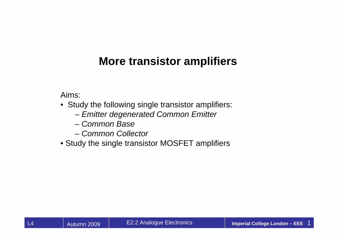
The 2nd form of the Miller theorem• consider an impedance connected in series with the common terminal of a current
amplifier of gain H.
• Looking from the input, the voltage developed on the feedback element is:
• Likewise, looking from the output, the amplifier has a gain=1/H, so the voltage developed on the feedback element is:
• the two diagrams above are equivalent in terms of their input and output impedances.
• NOTE: Only if the amplifier is ideal its current gain will not change as a result of the introduction of the Emitter degeneration resistor
( ) ( ) ( )1 2 1 1 , 1Z c c M in cV i i Z i Hi Z Z H Z= + = + ⇒ = +
,1 11 1Z c out M out cV Z i Z ZH H
⎛ ⎞ ⎛ ⎞= + ⇒ = +⎜ ⎟ ⎜ ⎟⎝ ⎠ ⎝ ⎠

Imperial College London – EEE 4L4 Autumn 2009 E2.2 Analogue Electronics
The emitter degenerated CE amplifier an application of the series version of the Miller theorem
A transistor has a current gain : 00CE
Cfe m
B v
ih g Ri πβ
=
∂= = =∂
The series version of the Miller theorem says:
The following two circuits have identical input and output impedances:
The emitter degenerated amplifier can be analysed as a common emitter amplifierdriven from a larger source impedance, and with an added impedance in series to the output!

Imperial College London – EEE 5L4 Autumn 2009 E2.2 Analogue Electronics
The emitter-degenerated common emitter amplifier
• Add a ZE to the common emitter amplifier • Schematically:
VCC
ZL
RE
ZS
VS
VCC
ZL
RE
ZS
VS
V=V(RE)
I=IE
IE
• The feedback network samples the emitter current. Since he emitter current is equal to the sum of the base and collector currents we can say that the feedback network (RE) samples both input an output current.
• The voltage developed on the feedback resistor is in series with VBE so the feedback voltage is mixed into the input voltage.
• This is an example of series-series feedback.

Imperial College London – EEE 6L4 Autumn 2009 E2.2 Analogue Electronics
“Miller Cancellation” and the narrowband high-gain RF amplifier:how to use negative feedback to overcome the GBW restriction
Vcc
Vdc +Vsig
Vout
• Inductive shunt-shunt (“Miller”) feedback is used to cancel CBC at signal frequencies. • An additional (big) DC block capacitor may be included in the feedback path.• As a result, the input impedance at signal frequencies is not subject to the Miller effect:
//in BEZ R Cπ=• The input admittance at resonance does not depend on the magnitude of the voltage gain. The input pole has been moved to a much higher frequency.• This technique is used to obtain very high voltage gain over a narrow signal band at radio frequencies, e.g. in antenna amplifiers.
At resonance:

Imperial College London – EEE 7L4 Autumn 2009 E2.2 Analogue Electronics
Common base amplifier
• The Common Base amplifier has the input at the emitter and the output at the collector. • The usual small signal model is not satisfactory; the gain element connects input and
output, not output and ground as is usual
• However, the controlled current source gm depends on its terminal voltage VE• We will set VB=0 ; if RBB is significant it can be viewed as series-series feedback.
• With a few simple circuit transformations the CB can be described by a “Pi” model.

Imperial College London – EEE 8L4 Autumn 2009 E2.2 Analogue Electronics
Common Base amplifier (2)• Add a loop of current sources of magnitude gmVE• Observe that the BE current source is controlled by its terminal voltages, so it is an impedance of magnitude 1/gm
The final form is the same as of CE amp.Notice that this is a NON INVERTING amp.Still, the analysis is identical of that of the CE amplifier, apart for the signs.

Imperial College London – EEE 9L4 Autumn 2009 E2.2 Analogue Electronics
Common Base amplifier (3)The AC analysis of the CB “Pi” model is same as for the Common Emitter amplifier.
Neglect the shunt-shunt Miller implicit feedback.Since this is a “Pi” network we can write the input admittance, voltage gain, milleradmittance and output impedance by inspection:
( )
( )
( )
1
/ /
1/1
inin m BE V CE m CE
in
outV m L A m L
in
m A CE
out S m S A
diY g sC A sC g sCdVdVA g Z R g ZdV
Y R sCZ Z g Z R
= + + + +
=
= +
+ +
In comparison to the CE amplifier:• Much larger (by a factor of β) input admittance• Same, but of opposite sign, transconcuctance• Output impedance depends strongly on signal source impedance.• Much smaller shunt-shunt Miller admittance, but with a resistive component!• Positive shunt-shunt Miller feedback. Input admittance may get inductive at high freq.

Imperial College London – EEE 10L4 Autumn 2009 E2.2 Analogue Electronics
Frequency response of the CB amplifier
Some observations on the frequency response of the CB amplifier:• The output pole is at roughly the same frequency as in the CE amplifier. • The input pole is at a much higher frequency than in the CE amplifier,
because of the much higher input admittance. As a result, • The common base amplifier IS NOT a dominant pole amplifier
• The shunt-shunt Miller feedback is positive. If CB is used with high voltage gain its input impedance may become inductive!
• Due to the positive Miller feedback, the bandwidth may increase with increasing voltage gain!• the CB configuration with high frequency transistors that have a small early voltage may even lead to a negative real part of the input impedance.
Uses of the CB amplifier:• Optical preamplifiers. Its small input impedance makes it a good current to
voltage converter . • As second stage in high frequency amplifiers (in “cascode” and differential
amplifiers)• Oscillators. The implicit positive feedback makes the CB prone to oscillation
Imperial College London – EEE 11L4 Autumn 2009 E2.2 Analogue Electronics
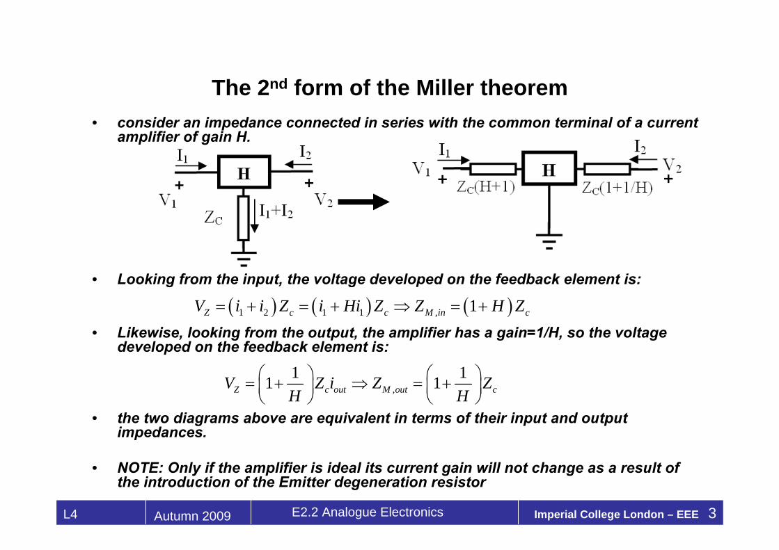
The Common Collector amplifier
From the analysis of the emitter degenerated CE amplifier we know the input impedance:
The voltage gain is simply:
1 1 since 1 1 / 1 1
out m in E m E m E mm
s in s m E s in m E m E
dV g Z Z g Z g Z ggdV Z Z g Z Z Z g Z g R
⎛ ⎞ ⎛ ⎞′′= ⎜ ⎟ ⎜ ⎟+ + + + +⎝ ⎠ ⎝ ⎠
( )( ) ( )( )0 01 1 / with // 1in in m L in BE V BCm
Z Z g Z Z C A Cgββ β= + + = + +
• Uses: Power amplifier or unity voltage buffer• Medium-high input impedance• Low output impedance• The load is connected in series-series feedback!• The topology has implicit positive feedback.
Imperial College London – EEE 12L4 Autumn 2009 E2.2 Analogue Electronics
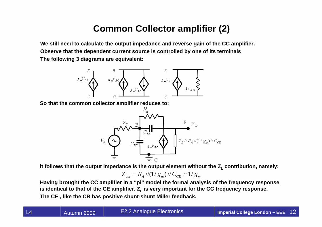
Common Collector amplifier (2)We still need to calculate the output impedance and reverse gain of the CC amplifier.Observe that the dependent current source is controlled by one of its terminalsThe following 3 diagrams are equivalent:
So that the common collector amplifier reduces to:
it follows that the output impedance is the output element without the ZL contribution, namely://(1/ ) // 1/out A m CE mZ R g C g=
Having brought the CC amplifier in a “pi” model the formal analysis of the frequency response is identical to that of the CE amplifier. ZL is very important for the CC frequency response. The CE , like the CB has positive shunt-shunt Miller feedback.
Imperial College London – EEE 13L4 Autumn 2009 E2.2 Analogue Electronics
Biasing transistor amplifiers
• We pay little attention in these notes on how the DC operating point of a transistor amplifier is established.
• Any one of the biasing schemes studied in the first year will be assumed.• This usually means that we need to consider an additional impedance to ground
describing the Thevenin impedance of the biasing circuit. • The bias network thevenin impedances are NOT shown in these notes, but must be
always be included in a real problem analysis. • DC bias networks are always designed to implement the following logic:
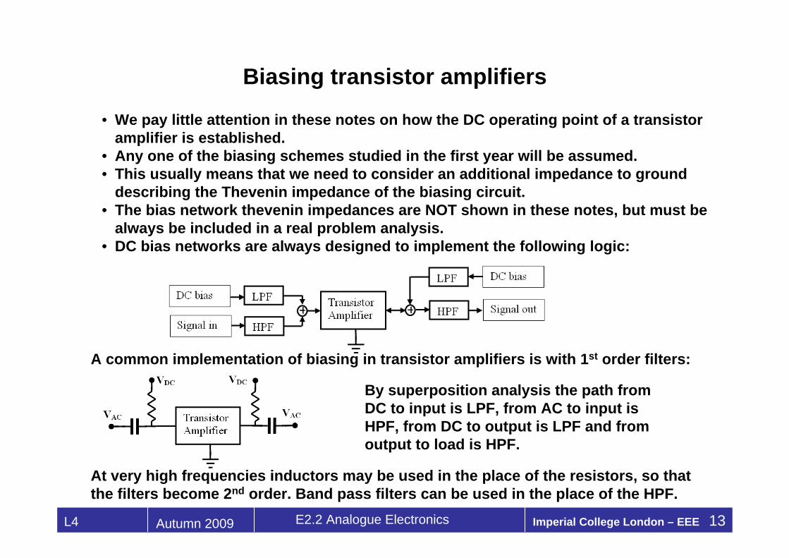
A common implementation of biasing in transistor amplifiers is with 1st order filters:
At very high frequencies inductors may be used in the place of the resistors, so that the filters become 2nd order. Band pass filters can be used in the place of the HPF.
By superposition analysis the path from DC to input is LPF, from AC to input is HPF, from DC to output is LPF and from output to load is HPF.

Imperial College London – EEE 14L4 Autumn 2009 E2.2 Analogue Electronics
Summary:Single stage BJT amplifiers
• A 3 terminal device can support 6 permutations of terminals• 3 of the 6 connections can give power gain (are amplifiers!) • The other 3 cannot give power gain and ARE NOT amplifiers.• The possible connections for a BJT are:
*
Transistor amplifiers are named according to which terminal is common.There are Common Emitter (CE), Common Collector (CC) and Common Base (CB) amplifiers. * The CC is also called the “emitter follower”
Imperial College London – EEE 15L4 Autumn 2009 E2.2 Analogue Electronics
MOSFET amplifiers
• Operation of MOSFET - revisited• Circuit models of MOSFET • MOSFET as a current amplifier: The transit frequency FT• The single stage FET amplifiers:
– Common Source– Common Drain– Common Gate

Imperial College London – EEE 16L4 Autumn 2009 E2.2 Analogue Electronics
MOSFET regions of operation
Log Idrain with VGS Drift and diffusion current components

Imperial College London – EEE 17L4 Autumn 2009 E2.2 Analogue Electronics
• In Common Source connection it is a transconductance amplifier.In the saturation region:
In the triode region:
• FETs can also operate in the “subthreshold” region, where they behave almost like BJTs:
• N is called the “subthreshold slope”• The usual definitions for transconductance, output conductance apply• Remember there is still no DC gate current• The subthreshold region extends for gate voltage excursions of a few kT
(around approx 50mV above threshold and 25 mV below threshold)• The current obeys the exponential law over 1-3 decades of magnitude.
Large signal description of a MOSFET
( ) ( )21
2ds ox gs T dsWI C V V VL
μ λ= − +
( )2 2D DS GS T DSI V V V Vβ= − −
( )/ /1 GS th D thV nV V VDS
WI e eL
μ −∝ −

Imperial College London – EEE 18L4 Autumn 2009 E2.2 Analogue Electronics
a small signal model for the MOSFET
• The MOSFET has 4 terminals: Gate, Source, Drain, Body• The static small signal model below is useful to frequencies of up to a few GHz. • Each transistor in a circuit is replaced by this model• The small signal model is similar that of the BJT with some minor differences:
– The DC conductance from Gate to source is aero– The body connection which acts as a second gate with a transconductance of
approximate magnitude gmb =0.2 gm• The body is usually connected to the source. • If the body is NOT connected to the source it is interpreted as explicit feedback.
Since it adds to the input voltage it is treated as Series at the input feedback
Imperial College London – EEE 19L4 Autumn 2009 E2.2 Analogue Electronics
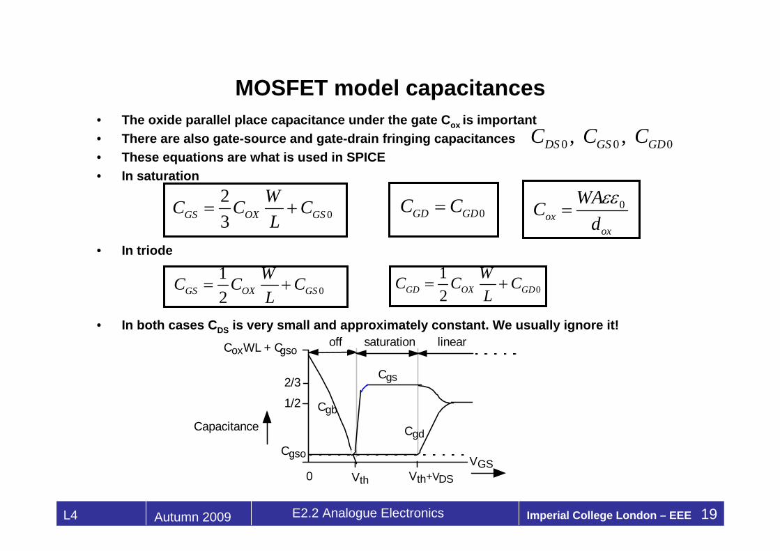
MOSFET model capacitances• The oxide parallel place capacitance under the gate Cox is important• There are also gate-source and gate-drain fringing capacitances• These equations are what is used in SPICE• In saturation
• In triode
• In both cases CDS is very small and approximately constant. We usually ignore it!
023GS OX GS
WC C CL
= + 0GD GDC C=
012GS OX GS
WC C CL
= + 012GD OX GD
WC C CL
= +
Cgs
Cgb
Cgd
2/3
1/2
VGS
off saturation linear
Vth Vth+VDS
CoxWL + Cgso
Capacitance
Cgso
0
0ox
ox
WACdεε
=
0 0 0, , DS GS GDC C C

Imperial College London – EEE 20L4 Autumn 2009 E2.2 Analogue Electronics
the FET transit (“transition”) frequency: fT
( )
( )
( )
21
1
12
D GS GS GD
D m GS
mDfe
G GS GD
m T
GS GD T
mT
GS GD
I V s C CI g V
gIh hI s C C
g fs C C s f
gfC C
τ
π
= + ⎫⎪⇒⎬= ⎪⎭
= = = =+
= = =+
=+
Note that this is the same expression as for the BJT fT with CBE CGS and CBC CGD

Imperial College London – EEE 21L4 Autumn 2009 E2.2 Analogue Electronics
Single stage FET amplifiersFET amplifier configurations are identical to those of BJT amplifiers with B G, E S, C D The circuit analysis is identical, so we will not repeat it.A few minor differences are:• the absence of • the body terminal which can be used as a second, lower gain gate , e.g. for mixers or for
explicit feedback. • The body controlled transconductance is approx 0.2 that of the gate, but of opposite sign• The transconductance of a FET is much lower than that of a BJT at the same bias current• Consequently impedance levels tend to be much higher• We usually control the gate width. This is equivalent to connecting many FET devices in
parallel• The following are all the possible single stage FET amplifiers:
Rπ

Imperial College London – EEE 22L4 Autumn 2009 E2.2 Analogue Electronics
Conclusions: Single transistor amplifiers
• Transistors are 3 terminal devices. Both BJT and FET have:– A low impedance terminal called the Emitter of the Source– A control Terminal called the Base or the Gate– A high real impedance terminal called the Collector or the Drain
• These terminals have the same function to the vacuum triode terminals: Filament (Emitter, Source), Grid (Base, Gate) and Plate (Collector, Drain)
• 3 of the possible 6 connections exhibit signal power gain:
Transistor amplifier calculations are similar to non-ideal op-amp circuit calculations