Embed Size (px)
Citation preview
LA G6SP - Dual binning
1 Version 1.6 | 2018-08-08
Produktdatenblatt | Version 1.1 www.osram-os.com
LA G6SP - Dual binning
Advanced Power TOPLED® Advanced Power TOPLED features a compact pack-age with a wide brightness range and high luminous efficiency.
Applications — Signalling
Features: — Package: white SMT package, colorless clear silicone resin
— Chip technology: Thinfilm
— Typ. Radiation: 120° (Lambertian emitter)
— Color: λdom = 617 nm (● amber)
— Optical efficacy: 84 lm/W
— Corrosion Robustness Class: 3B
— Qualifications: The product qualification test plan is based on the guidelines of AEC-Q101-REV-C, Stress Test Qualification for Automotive Grade Discrete Semiconductors. — ESD: 2 kV acc. to ANSI/ESDA/JEDEC JS-001 (HBM, Class 2)

LA G6SP - Dual binning
2 Version 1.6 | 2018-08-08
Ordering Information
Type Luminous Intensity 1) Luminous Intensity 1) Ordering CodeIF = 10 mA IF = 140 mAIv Iv
LA G6SP-T2U2-1-1+DBFA-24-1 355 ... 710 mcd 5.6 ... 14.0 cd Q65111A6792
LA G6SP - Dual binning
3 Version 1.6 | 2018-08-08
Maximum RatingsParameter Symbol Values
Operating Temperature Top min. max.
-40 °C 110 °C
Storage Temperature Tstg min. max.
-40 °C 110 °C
Junction Temperature Tj max. 125 °C
Junction Temperature for short time applications* Tj max. 150 °C
Forward current TS = 25 °C
IF min. max.
5 mA 200 mA
Surge Current t ≤ 10 µs; D = 0.005 ; TS = 25 °C
IFS max. 1000 mA
Reverse voltage 2) TS = 25 °C
VR max. 12 V
ESD withstand voltage acc. to ANSI/ESDA/JEDEC JS-001 (HBM, Class 2)
VESD 2 kV
*The median lifetime (L70/B50) for Tj =150°C is 100h.
LA G6SP - Dual binning
4 Version 1.6 | 2018-08-08
CharacteristicsIF = 140 mA; TS = 25 °C
Parameter Symbol Values
Peak Wavelength 3) λpeak typ. 625 nm
Dominant Wavelength 3) IF = 140 mA
λdom min. typ. max.
612 nm 617 nm 624 nm
Spectral Bandwidth at 50% Irel,max ∆λ typ. 18 nm
Viewing angle at 50 % IV 2φ typ. 120 °
Forward Voltage 4) IF = 140 mA
VF min. typ. max.
1.90 V 2.15 V 2.50 V
Reverse current 2) VR = 12 V
IR typ. max.
0.01 µA 10 µA
Real thermal resistance junction/solderpoint 5) RthJS real typ. max.
50 K / W 60 K / W
Electrical thermal resistance junction/solderpoint 5) with efficiency ηe = 32 %
RthJS elec. typ. max.
34 K / W 41 K / W
LA G6SP - Dual binning
5 Version 1.6 | 2018-08-08
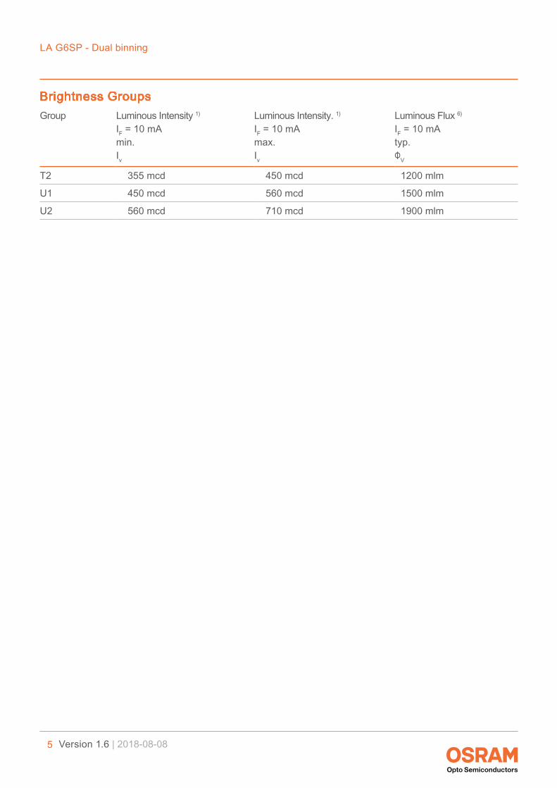
Brightness Groups
Group Luminous Intensity 1) Luminous Intensity. 1) Luminous Flux 6)
IF = 10 mA IF = 10 mA IF = 10 mAmin. max. typ.Iv Iv ΦV
T2 355 mcd 450 mcd 1200 mlm
U1 450 mcd 560 mcd 1500 mlm
U2 560 mcd 710 mcd 1900 mlm
LA G6SP - Dual binning
6 Version 1.6 | 2018-08-08
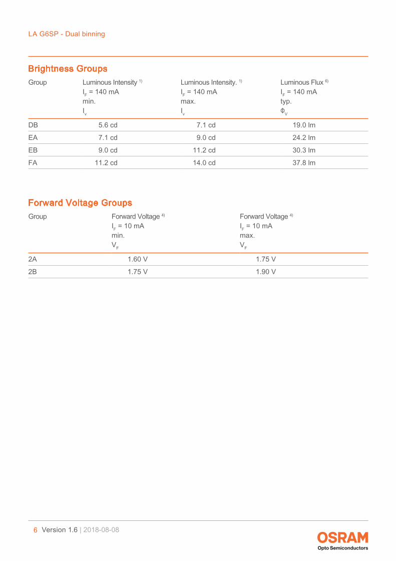
Brightness Groups
Group Luminous Intensity 1) Luminous Intensity. 1) Luminous Flux 6)
IF = 140 mA IF = 140 mA IF = 140 mAmin. max. typ.Iv Iv ΦV
DB 5.6 cd 7.1 cd 19.0 lm
EA 7.1 cd 9.0 cd 24.2 lm
EB 9.0 cd 11.2 cd 30.3 lm
FA 11.2 cd 14.0 cd 37.8 lm
Forward Voltage Groups
Group Forward Voltage 4) Forward Voltage 4)
IF = 10 mA IF = 10 mAmin. max.VF VF
2A 1.60 V 1.75 V
2B 1.75 V 1.90 V
LA G6SP - Dual binning
7 Version 1.6 | 2018-08-08
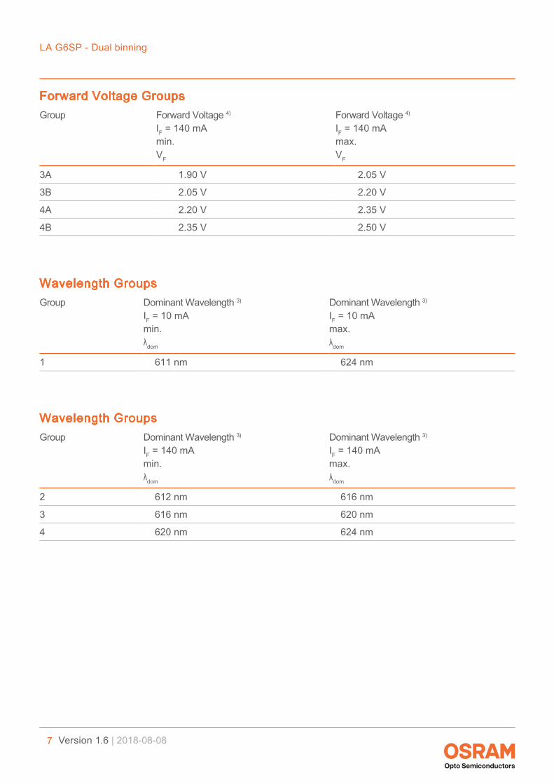
Forward Voltage Groups
Group Forward Voltage 4) Forward Voltage 4)
IF = 140 mA IF = 140 mAmin. max.VF VF
3A 1.90 V 2.05 V
3B 2.05 V 2.20 V
4A 2.20 V 2.35 V
4B 2.35 V 2.50 V
Wavelength Groups
Group Dominant Wavelength 3) Dominant Wavelength 3)
IF = 10 mA IF = 10 mAmin. max.λdom λdom
1 611 nm 624 nm
Wavelength Groups
Group Dominant Wavelength 3) Dominant Wavelength 3)
IF = 140 mA IF = 140 mAmin. max.λdom λdom
2 612 nm 616 nm
3 616 nm 620 nm
4 620 nm 624 nm
LA G6SP - Dual binning
8 Version 1.6 | 2018-08-08
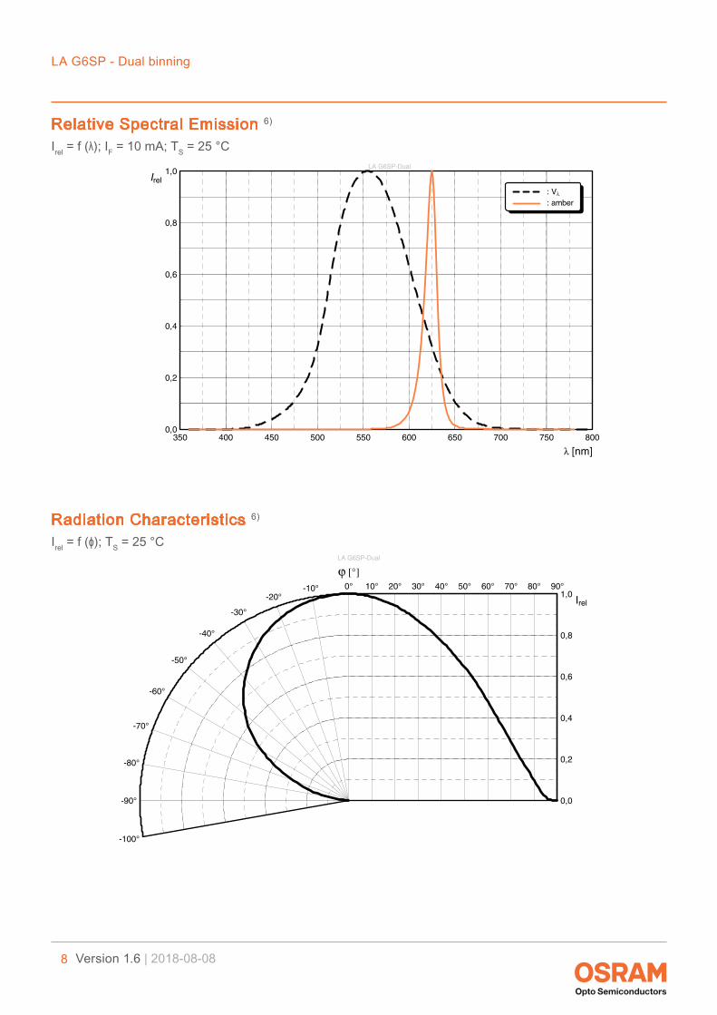
LA G6SP-Dual
350 400 450 500 550 600 650 700 750 800
λ [nm]
0,0
0,2
0,4
0,6
0,8
1,0Irel
: Vλ
: amber
Relative Spectral Emission 6) Irel = f (λ); IF = 10 mA; TS = 25 °C
LA G6SP-Dual
-100°
-90°
-80°
-70°
-60°
-50°
-40°
-30°
-20°-10° 0° 10° 20° 30° 40° 50° 60° 70° 80° 90°
ϕ [°]
0,0
0,2
0,4
0,6
0,8
1,0Irel
Radiation Characteristics 6) Irel = f (ϕ); TS = 25 °C
LA G6SP - Dual binning
9 Version 1.6 | 2018-08-08
LA G6SP-Dual
5 10 20 30 40 50 100
200
IF [mA]
0,05
0,1
0,5
1
5
10
IVIV(IF group) : If group = 140mA
: If group = 10mA
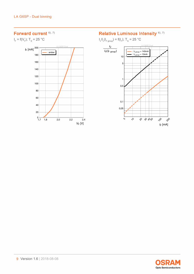
Relative Luminous Intensity 6), 7)
Iv/Iv(IF group) = f(IF); TS = 25 °C
LA G6SP-Dual
1,7 1,8 2,0 2,2 2,4
VF [V]
5
20
40
60
80
100
120
140
160
180
200IF [mA]
: amber
Forward current 6), 7)
IF = f(VF); TS = 25 °C
LA G6SP - Dual binning
10 Version 1.6 | 2018-08-08
LA G6SP-Dual
-40 -20 0 20 40 60 80 100 120
Tj [°C]
0,0
0,2
0,4
0,6
0,8
1,0
1,2
1,4
1,6IvIv(25°C) : amber
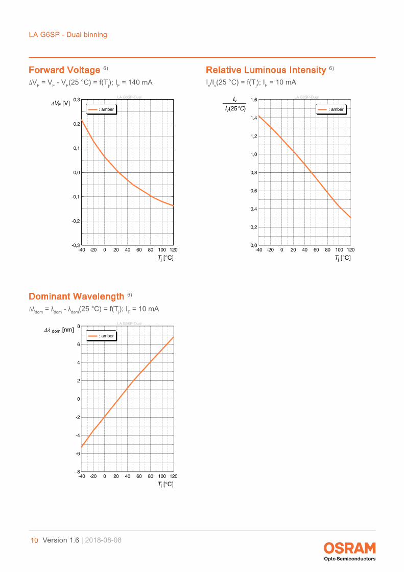
Relative Luminous Intensity 6)
Iv/Iv(25 °C) = f(Tj); IF = 10 mA
LA G6SP-Dual
-40 -20 0 20 40 60 80 100 120
Tj [°C]
-0,3
-0,2
-0,1
0,0
0,1
0,2
0,3∆VF [V]
: amber
Forward Voltage 6)
∆VF = VF - VF(25 °C) = f(Tj); IF = 140 mA
LA G6SP-Dual
-40 -20 0 20 40 60 80 100 120
Tj [°C]
-8
-6
-4
-2
0
2
4
6
8∆λ dom [nm]
: amber
Dominant Wavelength 6)
∆λdom = λdom - λdom(25 °C) = f(Tj); IF = 10 mA

LA G6SP - Dual binning
11 Version 1.6 | 2018-08-08
00
˚C
T
IFmA
OHL02180
TA TS
ATTS temp. solder point
temp. ambient
50
100
150
200
250
20 40 60 80 120
Max. Permissible Forward CurrentIF = f(T)
0-5
FI A tP=D T
tp
s
0.20.5
0.05
1
0.1
OHL01185
0.02
0.0050.01
=D
T
tP
IF
-410 -310 -210 -110 010 110 21010
0.033
0.2
0.4
0.6
0.8
1.0
1.2
Permissible Pulse Handling CapabilityIF = f(tp); D: Duty cycle; TS = 85 °C
0-5
FI A tP=D T
tp
s
0.20.5
0.05
1
0.1
OHL01184
0.02
0.0050.01
=D
T
tP
IF
-410 -310 -210 -110 010 110 21010
0.033
0.2
0.4
0.6
0.8
1.0
1.2
Permissible Pulse Handling CapabilityIF = f(tp); D: Duty cycle; TS = 25 °C

LA G6SP - Dual binning
12 Version 1.6 | 2018-08-08
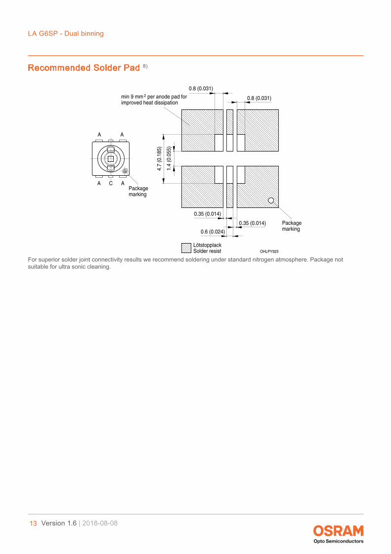
Dimensional Drawing 8)
Approximate Weight: 40.0 mg
Package marking: Cathode
Corrosion test: Class: 3B Test condition: 40°C / 90 % RH / 15 ppm H2S / 14 days (stricter then IEC 60068-2-43)
LA G6SP - Dual binning
13 Version 1.6 | 2018-08-08
For superior solder joint connectivity results we recommend soldering under standard nitrogen atmosphere. Package not suitable for ultra sonic cleaning.
Recommended Solder Pad 8)
Packagemarking
0.6 (0.024)
LötstopplackSolder resist
0.35 (0.014)
A
A
1.4
(0.0
55)
min 9 mm per anode pad forimproved heat dissipation
C A
A
4.7
(0.1
85)
2
0.8 (0.031)
OHLPY925
0.35 (0.014)
0.8 (0.031)
Packagemarking
LA G6SP - Dual binning
14 Version 1.6 | 2018-08-08
Reflow Soldering ProfileProduct complies to MSL Level 2 acc. to JEDEC J-STD-020E
00
s
OHA04525
50
100
150
200
250
300
50 100 150 200 250 300t
T
˚C
St
t
Pt
Tp240 ˚C
217 ˚C
245 ˚C
25 ˚C
L
Profile Feature Symbol Pb-Free (SnAgCu) Assembly UnitMinimum Recommendation Maximum
Ramp-up rate to preheat*)
25 °C to 150 °C2 3 K/s
Time tSTSmin to TSmax
tS 60 100 120 s
Ramp-up rate to peak*)
TSmax to TP
2 3 K/s
Liquidus temperature TL 217 °C
Time above liquidus temperature tL 80 100 s
Peak temperature TP 245 260 °C
Time within 5 °C of the specified peaktemperature TP - 5 K
tP 10 20 30 s
Ramp-down rate*TP to 100 °C
3 6 K/s
Time25 °C to TP
480 s
All temperatures refer to the center of the package, measured on the top of the component* slope calculation DT/Dt: Dt max. 5 s; fulfillment for the whole T-range
LA G6SP - Dual binning
15 Version 1.6 | 2018-08-08
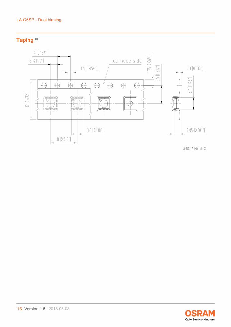
Taping 8)
LA G6SP - Dual binning
16 Version 1.6 | 2018-08-08
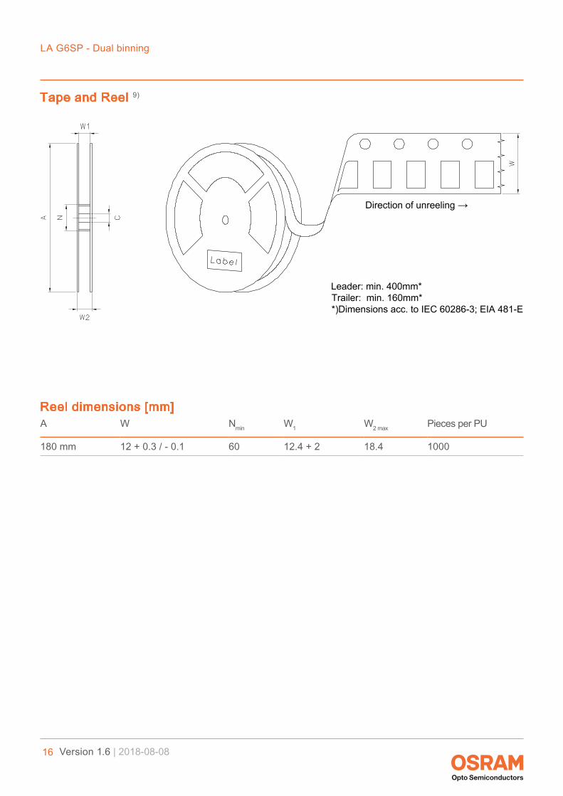
Tape and Reel 9)
Reel dimensions [mm]A W Nmin W1 W2 max Pieces per PU
180 mm 12 + 0.3 / - 0.1 60 12.4 + 2 18.4 1000
LA G6SP - Dual binning
17 Version 1.6 | 2018-08-08
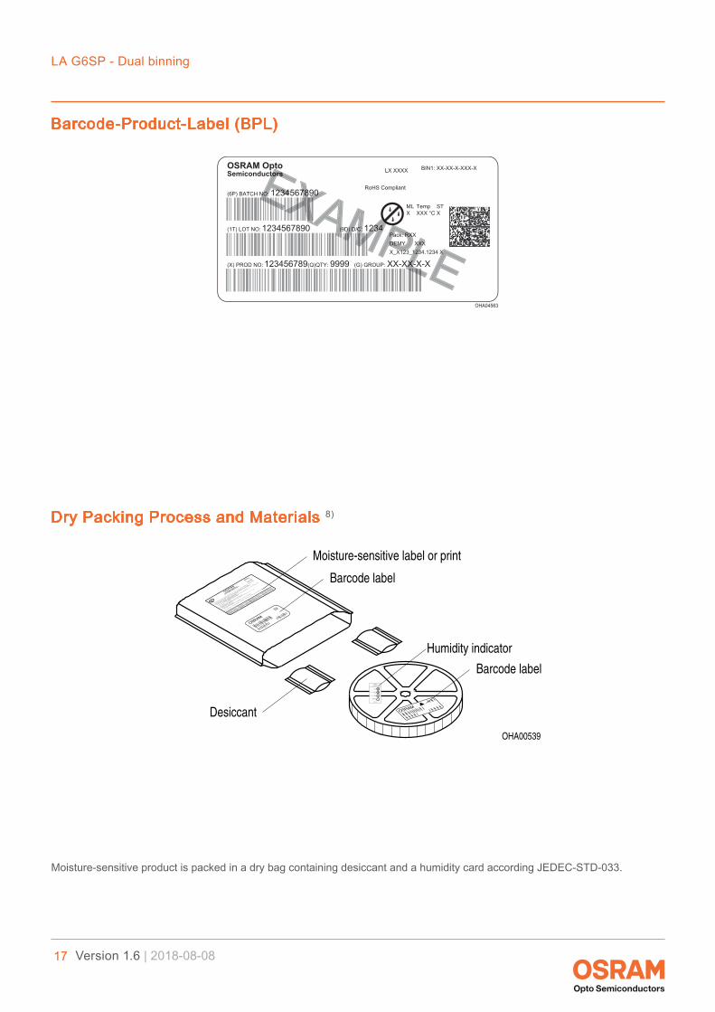
Barcode-Product-Label (BPL)
Moisture-sensitive product is packed in a dry bag containing desiccant and a humidity card according JEDEC-STD-033.
Dry Packing Process and Materials 8)
OHA00539
OSRAM
Moisture-sensitive label or print
Barcode label
Desiccant
Humidity indicator
Barcode label
OSRAM
Please check the HIC immidiately afterbag opening.
Discard if circles overrun.Avoid metal contact.
WET
Do not eat.
Comparatorcheck dot
parts still adequately dry.
examine units, if necessary
examine units, if necessary
5%
15%
10%bake units
bake units
If wet,
change desiccant
If wet,
Humidity IndicatorMIL-I-8835
If wet,
Mois
ture
Level 3
Flo
or tim
e 168 H
ours
Mois
ture
Level 6
Flo
or tim
e 6
Hours
a) H
umid
ity In
dicato
r C
ard is
> 1
0% w
hen read a
t 23 ˚
C ±
5 ˚C
, or
reflo
w, v
apor-phase r
eflow
, or equiv
alent p
rocessin
g (peak p
ackage
2. Afte
r th
is b
ag is o
pened, devic
es that w
ill b
e subje
cted to
infrare
d
1. Shelf
life in
seale
d bag: 2
4 month
s at <
40 ˚
C a
nd < 9
0% rela
tive h
umid
ity (R
H).
Mois
ture
Level 5
a
at facto
ry c
onditions o
f
(if b
lank, s
eal date
is id
entical w
ith d
ate c
ode).
a) M
ounted w
ithin
b) S
tore
d at
body tem
p.
3. Devic
es require
bakin
g, befo
re m
ounting, i
f:
Bag s
eal date
Mois
ture
Level 1
Mois
ture
Level 2
Mois
ture
Level 2
a4. If b
aking is
require
d,
b) 2a o
r 2b is
not m
et.
Date
and ti
me o
pened:
refe
rence IP
C/J
ED
EC
J-S
TD
-033 fo
r bake p
rocedure
.
Flo
or tim
e see b
elow
If bla
nk, see b
ar code la
bel
Flo
or tim
e > 1
Year
Flo
or tim
e 1
Year
Flo
or tim
e 4
Weeks10%
RH
.
_<
Mois
ture
Level 4
Mois
ture
Level 5
˚C).
OPTO
SEM
ICO
NDUCTORS
MO
ISTURE S
ENSITIV
E
This b
ag conta
ins
CAUTION
Flo
or tim
e 72 H
ours
Flo
or tim
e 48 H
ours
Flo
or tim
e 24 H
ours
30 ˚C
/60%
RH
.
_<
LE
VE
L
If bla
nk, see
bar code la
bel
LA G6SP - Dual binning
18 Version 1.6 | 2018-08-08
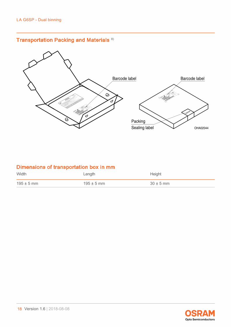
Transportation Packing and Materials 8)
OHA02044
PACKVAR:
R077Additional TEXT
P-1+Q-1
Multi TOPLED
Muste
r
OSRAM Opto
Semiconductors
(6P) BATCH NO:
(X) PROD NO:
10
(9D) D/C:
11(1T) LOT NO:
210021998
123GH1234
024 5
(Q)QTY: 2000
0144
(G) GROUP:
260 C RT240 C R
3
220 C R
MLBin3:Bin2: Q
-1-20
Bin1: P-1-20
LSY T6762
2a
Temp ST
R18DEMY
PACKVAR:
R077Additional TEXT
P-1+Q-1
Multi TOPLED
Muste
r
OSRAM Opto
Semiconductors
(6P) BATCH NO:
(X) PROD NO:
10
(9D) D/C:
11(1T) LOT NO:
210021998
123GH1234
024 5
(Q)QTY: 2000
0144
(G) GROUP:
260 C RT240 C R
3
220 C R
MLBin3:Bin2: Q
-1-20
Bin1: P-1-20
LSY T6762
2a
Temp ST
R18DEMY
OSRAM
Packing
Sealing label
Barcode label
Mois
ture
Level 3
Flo
or tim
e 168 H
ours
Mois
ture
Level 6
Flo
or tim
e 6
Hours
a) H
umid
ity In
dicato
r C
ard is
> 1
0% w
hen read a
t 23 ˚
C ±
5 ˚C
, or
reflo
w, v
apor-phase r
eflow
, or e
quivale
nt pro
cessing (p
eak package
2. Afte
r th
is b
ag is o
pened,
devices th
at will
be s
ubjecte
d to in
frare
d
1. Shelf
life in
seale
d bag: 2
4 month
s at <
40 ˚
C a
nd < 9
0% rela
tive h
umid
ity (R
H).
Mois
ture
Level 5
a
at facto
ry c
onditions o
f
(if b
lank, s
eal date
is id
entical w
ith d
ate c
ode).
a) M
ounted w
ithin
b) S
tore
d at
body te
mp.
3. Devic
es require
bakin
g, befo
re m
ounting, i
f:
Bag s
eal date
Mois
ture
Level 1
Mois
ture
Level 2
Mois
ture
Level 2
a4. If b
aking is
require
d,
b) 2a o
r 2b is
not m
et.
Date
and ti
me o
pened:
refe
rence IP
C/J
ED
EC
J-S
TD-0
33 for bake p
rocedure
.
Floor
time s
ee belo
w
If bla
nk, see b
ar code la
bel
Flo
or tim
e > 1
Year
Floor
time
1 Y
ear
Flo
or tim
e 4
Weeks10%
RH
.
_<
Mois
ture
Level 4
Mois
ture
Level 5
˚C).
OPTO
SEM
ICONDUCTO
RS
MO
ISTURE S
ENSITIV
E
This b
ag conta
ins
CAUTION
Flo
or tim
e 72 H
ours
Flo
or tim
e 48 H
ours
Flo
or tim
e 24 H
ours
30 ˚C
/60%
RH
.
_<
LE
VE
L
If bla
nk, see
bar code la
bel
Barcode label
Dimensions of transportation box in mmWidth Length Height
195 ± 5 mm 195 ± 5 mm 30 ± 5 mm
LA G6SP - Dual binning
19 Version 1.6 | 2018-08-08
NotesThe evaluation of eye safety occurs according to the standard IEC 62471:2006 (photo biological safety of lamps and lamp systems). Within the risk grouping system of this IEC standard, the device specified in this data sheet falls into the class exempt group (exposure time 10000 s). Under real circumstances (for expo-sure time, conditions of the eye pupils, observation distance), it is assumed that no endangerment to the eye exists from these devices. As a matter of principle, however, it should be mentioned that intense light sources have a high secondary exposure potential due to their blinding effect. When looking at bright light sources (e.g. headlights), temporary reduction in visual acuity and afterimages can occur, leading to irrita-tion, annoyance, visual impairment, and even accidents, depending on the situation.
Subcomponents of this device contain, in addition to other substances, metal filled materials including silver. Metal filled materials can be affected by environments that contain traces of aggressive substances. There-fore, we recommend that customers minimize device exposure to aggressive substances during storage, production, and use. Devices that showed visible discoloration when tested using the described tests above did show no performance deviations within failure limits during the stated test duration. Respective failure limits are described in the IEC60810.
For further application related informations please visit www.osram-os.com/appnotes
LA G6SP - Dual binning
20 Version 1.6 | 2018-08-08
Disclaimer
DisclaimerLanguage english will prevail in case of any discrepancies or deviations between the two language word-ings.
Attention please!The information describes the type of component and shall not be considered as assured characteristics. Terms of delivery and rights to change design reserved. Due to technical requirements components may contain dangerous substances.For information on the types in question please contact our Sales Organization.If printed or downloaded, please find the latest version on the OSRAM OS webside.
PackingPlease use the recycling operators known to you. We can also help you – get in touch with your nearest sales office.By agreement we will take packing material back, if it is sorted. You must bear the costs of transport. For packing material that is returned to us unsorted or which we are not obliged to accept, we shall have to invoice you for any costs incurred.
Product safety devices/applications or medical devices/applicationsOSRAM OS components are not developed, constructed or tested for the application as safety relevant component or for the application in medical devices.
In case Buyer – or Customer supplied by Buyer– considers using OSRAM OS components in product safety devices/applications or medical devices/applications, Buyer and/or Customer has to inform the local sales partner of OSRAM OS immediately and OSRAM OS and Buyer and /or Customer will analyze and coordi-nate the customer-specific request between OSRAM OS and Buyer and/or Customer.
LA G6SP - Dual binning
21 Version 1.6 | 2018-08-08
Glossary1) Brightness: Brightness values are measured during a current pulse of typically 25 ms, with an internal
reproducibility of ±8 % and an expanded uncertainty of ±11 % (acc. to GUM with a coverage factor of k = 3).
2) Reverse Operation: Reverse Operation of 10 hours is permissible in total. Continuous reverse opera-tion is not allowed.
3) Wavelength: The wavelength is measured at a current pulse of typically 25 ms, with an internal repro-ducibility of ±0.5 nm and an expanded uncertainty of ±1 nm (acc. to GUM with a coverage factor of k = 3).
4) Forward Voltage: The forward voltage is measured during a current pulse of typically 8 ms, with an internal reproducibility of ±0.05 V and an expanded uncertainty of ±0.1 V (acc. to GUM with a coverage factor of k = 3).
5) Thermal Resistance: Rth max is based on statistic values (6σ).6) Typical Values: Due to the special conditions of the manufacturing processes of semiconductor devic-
es, the typical data or calculated correlations of technical parameters can only reflect statistical figures. These do not necessarily correspond to the actual parameters of each single product, which could dif-fer from the typical data and calculated correlations or the typical characteristic line. If requested, e.g. because of technical improvements, these typ. data will be changed without any further notice.
7) Characteristic curve: In the range where the line of the graph is broken, you must expect higher differ-ences between single devices within one packing unit.
8) Tolerance of Measure: Unless otherwise noted in drawing, tolerances are specified with ±0.1 and dimensions are specified in mm.
9) Tape and Reel: All dimensions and tolerances are specified acc. IEC 60286-3 and specified in mm.
LA G6SP - Dual binning
22 Version 1.6 | 2018-08-08
Published by OSRAM Opto Semiconductors GmbH Leibnizstraße 4, D-93055 Regensburg www.osram-os.com © All Rights Reserved.