Embed Size (px)
Citation preview
LAB 12: Arithmetic Logic Unit
By: Daniel Stumpp
Performed: 4/6/2019
Written: 4/9/2019
1
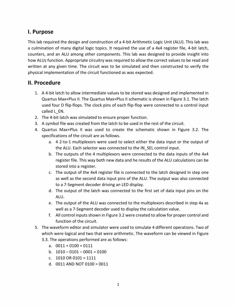
I. Purpose
This lab required the design and construction of a 4-bit Arithmetic Logic Unit (ALU). This lab was
a culmination of many digital logic topics. It required the use of a 4x4 register file, 4-bit latch,
counters, and an ALU among other components. This lab was designed to provide insight into
how ALUs function. Appropriate circuitry was required to allow the correct values to be read and
written at any given time. The circuit was to be simulated and then constructed to verify the
physical implementation of the circuit functioned as was expected.
II. Procedure
1. A 4-bit latch to allow intermediate values to be stored was designed and implemented in
Quartus Max+Plus II. The Quartus Max+Plus II schematic is shown in Figure 3.1. The latch
used four D flip-flops. The clock pins of each flip-flop were connected to a control input
called L_EN.
2. The 4-bit latch was simulated to ensure proper function.
3. A symbol file was created from the latch to be used in the rest of the circuit.
4. Quartus Max+Plus II was used to create the schematic shown in Figure 3.2. The
specifications of the circuit are as follows.
a. 4 2-to-1 multiplexors were used to select either the data input or the output of
the ALU. Each selector was connected to the IN_SEL control input.
b. The outputs of the 4 multiplexors were connected to the data inputs of the 4x4
register file. This way both new data and he results of the ALU calculations can be
stored into a register.
c. The output of the 4x4 register file is connected to the latch designed in step one
as well as the second data input pins of the ALU. The output was also connected
to a 7-Segment decoder driving an LED display.
d. The output of the latch was connected to the first set of data input pins on the
ALU.
e. The output of the ALU was connected to the multiplexors described in step 4a as
well as a 7-Segment decoder used to display the calculation value.
f. All control inputs shown in Figure 3.2 were created to allow for proper control and
function of the circuit.
5. The waveform editor and simulator were used to simulate 4 different operations. Two of
which were logical and two that were arithmetic. The waveform can be viewed in Figure
3.3. The operations performed are as follows:
a. 0011 + 0100 = 0111
b. 1010 – 0101 – 0001 = 0100
c. 1010 OR 0101 = 1111
d. 0011 AND NOT 0100 = 0011

2
6. A waveform was then created to add four hex digits and store the results in one of the
registers. Upon completion of this operation, three of the operands were to remain in
registers and the fourth was to contain the sum of the values. The operation chosen was
2 + 3 + 4 + 5 = E. The waveform produced can be seen in Figure 3.4.
7. Upon completion of the previous two waveforms, a waveform was produced to simulate
multiplication of 7 and 5. The full pseudocode is shown in Figure 3.5. Only the first partial
product was simulated on the waveform for expediency. This simulated waveform is
shown in Figure 3.6.
8. After completing the simulation of the circuit in Quartus Max+Plus II, the physical circuit
was implemented on a breadboard. All the control inputs in Figure 3.2 were implemented
using a switch. The carry input of the ALU was pulled high.
9. After the circuit was built, a LogicPort logic analyzer was used to check that the circuit
was operating properly. The operations in steps 5-7 were performed and the waveforms
produced were compared to the simulated waveforms to ensure that the output was as
expected. The various waveforms produced can be viewed below in the results section.
III. Results
In order to store intermediate values for calculations, a 4-bit latch was required. This latch was
created using 7474 Dual D flip-flop IC chips. The Quartus design is shown below in Figure 3.1.
Figure 3.1
4-bit latch design in Quartus
3
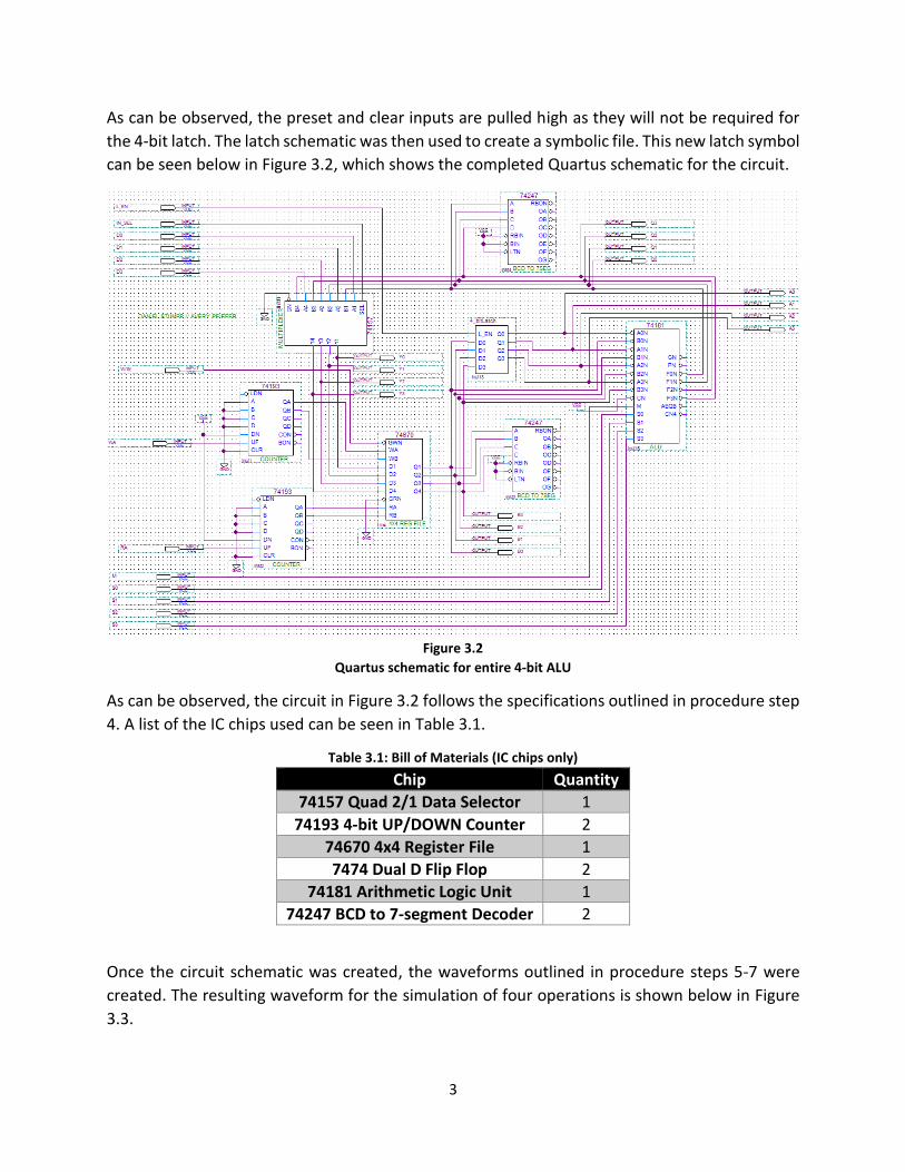
As can be observed, the preset and clear inputs are pulled high as they will not be required for
the 4-bit latch. The latch schematic was then used to create a symbolic file. This new latch symbol
can be seen below in Figure 3.2, which shows the completed Quartus schematic for the circuit.
Figure 3.2
Quartus schematic for entire 4-bit ALU
As can be observed, the circuit in Figure 3.2 follows the specifications outlined in procedure step
4. A list of the IC chips used can be seen in Table 3.1.
Table 3.1: Bill of Materials (IC chips only)
Chip Quantity
74157 Quad 2/1 Data Selector 1
74193 4-bit UP/DOWN Counter 2
74670 4x4 Register File 1
7474 Dual D Flip Flop 2
74181 Arithmetic Logic Unit 1
74247 BCD to 7-segment Decoder 2
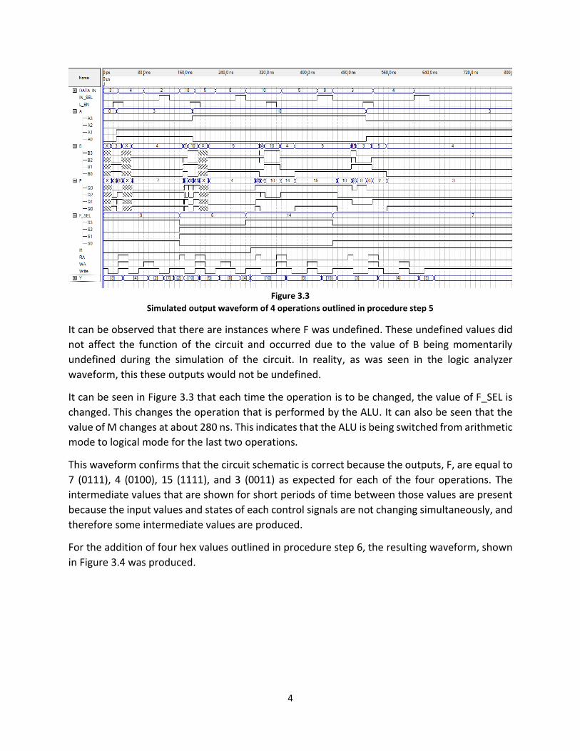
Once the circuit schematic was created, the waveforms outlined in procedure steps 5-7 were
created. The resulting waveform for the simulation of four operations is shown below in Figure
3.3.
4
Figure 3.3
Simulated output waveform of 4 operations outlined in procedure step 5
It can be observed that there are instances where F was undefined. These undefined values did
not affect the function of the circuit and occurred due to the value of B being momentarily
undefined during the simulation of the circuit. In reality, as was seen in the logic analyzer
waveform, this these outputs would not be undefined.
It can be seen in Figure 3.3 that each time the operation is to be changed, the value of F_SEL is
changed. This changes the operation that is performed by the ALU. It can also be seen that the
value of M changes at about 280 ns. This indicates that the ALU is being switched from arithmetic
mode to logical mode for the last two operations.
This waveform confirms that the circuit schematic is correct because the outputs, F, are equal to
7 (0111), 4 (0100), 15 (1111), and 3 (0011) as expected for each of the four operations. The
intermediate values that are shown for short periods of time between those values are present
because the input values and states of each control signals are not changing simultaneously, and
therefore some intermediate values are produced.
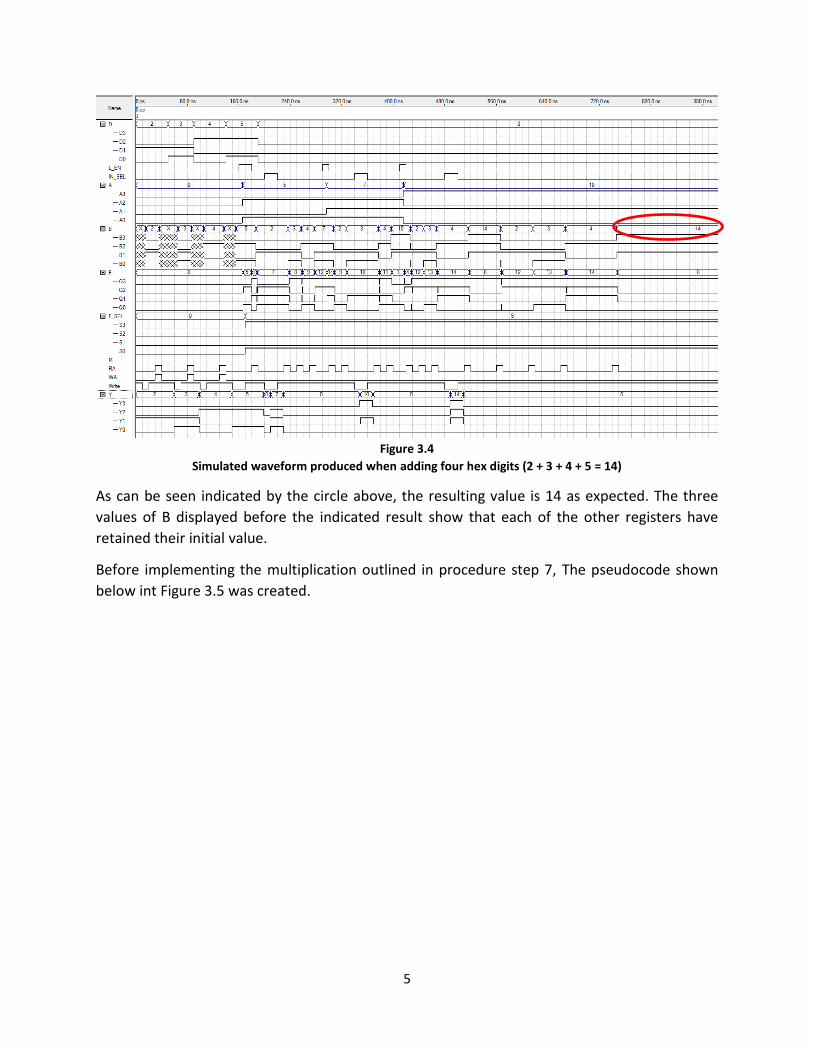
For the addition of four hex values outlined in procedure step 6, the resulting waveform, shown
in Figure 3.4 was produced.
5
Figure 3.4
Simulated waveform produced when adding four hex digits (2 + 3 + 4 + 5 = 14)
As can be seen indicated by the circle above, the resulting value is 14 as expected. The three
values of B displayed before the indicated result show that each of the other registers have
retained their initial value.
Before implementing the multiplication outlined in procedure step 7, The pseudocode shown
below int Figure 3.5 was created.

6
Figure 3.5
Pseudocode for multiplication. The time of the event in Figure 3.5 is indicated.
The implementation of the pseudocode using the waveform editor resulted in the following
waveform shown in Figure 3.6. The waveform is split up into two images for ease of viewing.

7
Figure 3.6
Simulated waveforms of multiplication of 7 and 5.
The waveform in Figure 3.6 shows the result of the first partial sum, which in this case resulted
in a value of 7 as can be seen indicated by an arrow on the bottom image. In order ensure that
there were no unforeseen anomalies, a second multiplication was performed, and the first partial
product waveform is shown below in Figure 3.7. The result was 6 as expected.
Figure 3.7
Simulated waveforms of multiplication of 6 and 3.
The circuit was constructed using a breadboard and then the same operations were performed
in order to confirm that the physical circuit was operating as expected. In Figures 3.8(a-d) below,
the operations from procedure step 5 can be observed.

8
Figure 3.8a
Logic analyzer waveform of operation 3 + 4
Figure 3.8b
Logic analyzer waveform of operation 10 – 5 -1
Figure 3.8c
Logic analyzer waveform of operation 10 OR 5

9
Figure 3.8d
Logic analyzer waveform of operation 3 AND NOT 4
Observation of the above waveforms shows that the results of each operation is correct. Note
that in some instances the hex value displayed on the waveform is incorrect. This is because the
software misinterpreted which bit in the group was the least significant. When observing each
bit of the groups it can be seen that the values are correct.
The addition of four hex digits as described in procedure step 6 was also performed with the
physical circuit and the resulting waveform was recorded using the logic analyzer. This waveform
is shown below in Figure 3.9. Note that it was split into two waveforms for ease of reading.
Figure 3.9
Logic analyzer waveform produced when adding four hex digits (2 + 3 + 4 + 5 = 14)
As can be observed circled in the waveform, the result is 0xE (14) which was expected. This
confirms proper function of the circuit for this operation.
10
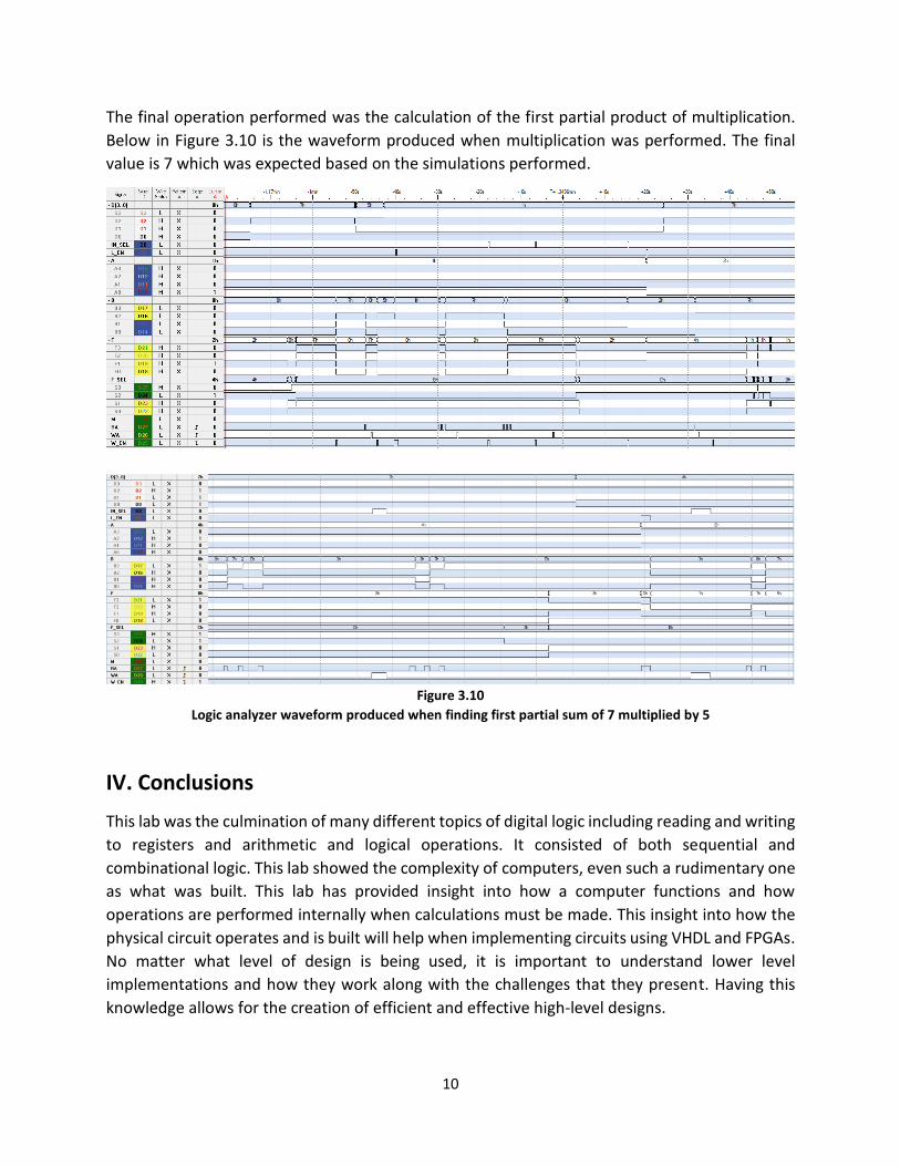
The final operation performed was the calculation of the first partial product of multiplication.
Below in Figure 3.10 is the waveform produced when multiplication was performed. The final
value is 7 which was expected based on the simulations performed.
Figure 3.10
Logic analyzer waveform produced when finding first partial sum of 7 multiplied by 5
IV. Conclusions
This lab was the culmination of many different topics of digital logic including reading and writing
to registers and arithmetic and logical operations. It consisted of both sequential and
combinational logic. This lab showed the complexity of computers, even such a rudimentary one
as what was built. This lab has provided insight into how a computer functions and how
operations are performed internally when calculations must be made. This insight into how the
physical circuit operates and is built will help when implementing circuits using VHDL and FPGAs.
No matter what level of design is being used, it is important to understand lower level
implementations and how they work along with the challenges that they present. Having this
knowledge allows for the creation of efficient and effective high-level designs.

11
V. References
A. E. Peiffer, Lab Partner.
A. K. Jones, Lab 12: A 4-bit ALU, http://www.engrclasses.pitt.edu/electrical/faculty-
staff/akjones/0501/web-docs/2019/spring/main.html.