Embed Size (px)
Citation preview

LAB 4
DC motor speed control using pulse
width modulation (PWM)
Submitted by
Vishal Bharam and Bicky Shakya
ENGR 323
Prof. Taikang Ning

Introduction
As we saw in the previous projects, 8051 microcontroller embedded into other systems can perform
multiple complicated operations at the same time. 8051 microcontrollers are used in a wide spectrum of
applications, such as in the field of automobiles, video games, microwaves and many others. In this
laboratory, we use the 8051 microcontroller to design an embedded system that would run according to
allowable target speed desired by the user.
Problem Statement: This design laboratory is to help us learn and become familiar with designing and
implementing a DC motor speed control embedded system, which involves Pulse-Width Modulation
(PWM) and the proportional, integral and derivative (PID) controller design.
Specific Design Goal: The design goal of this lab is to use the SilliconLab-C8051F120 kit to implement a
PID controller that allows the user to enter the desired target speed. With feedback, the PID controller can
make timely adjustment to the PWM to accommodate the changing shaft-load to maintain the desired
rotating speed. The system block diagram for the system is given in fig.1.
Fig 1: System configuration of DC motor speed control
Following constrains are to be taken into the consideration while designing the lab:
Allow users to easily adjust the desired motor rpm speed
Use the PWM signal to control the DC motor speed
Use the pushbutton to control the rotating direction
Implement a properly working adjustable feedback controller
Display the system information (desired speed and actual speed of the DC motor ) using a
16x2 LCD

Hardware:
Silicon Laboratories C8051F500DK:
For this lab, we used the SiliconLabs C8051F500DK evaluation board. The board consists of the 8051
microcontroller but with a lot of added features. Some of the features include a 12 bit analog-to-digital
converter, comparators, built in clock (24 MHz), 40 input/output pins and more. All in all, the
C8051F500 is designed to be a stand-alone ‘system on a chip’ solution, as claimed by the manufacturer.
The C8051F500 board was connected to the PC using the USB Debug Adapter to DEBUG_A on the
target board with the 10-pin ribbon cable as shown in the figure 2.
Fig.2: Hardware Setup of C8051F500 using a USB DEBUG Adapter
The C8051F500 also has two 12-bit Analog to Digital Converters (ADC). We connected one of the
ADC’s to the 1k potentiometer via P1.2 pin (A-22 on C8051F500 Female Socket). This allowed us to
easily adjust the desired speed. Also, the PWM generated from the C8051F500 was sent through P0.2
(A-12, CEX0) to the EN1,2 (Enable pin) on the H-Bridge. The pulses generated by the motor amplified
from the op-amp were to be counted using the counter 0. Thus, counter 0 which was counting the pulses
was connected to the pin P0.3 (C-11).

DC Motor:
For this lab, we used a 9V DC motor (model # ESCAP 28 D2R 11) with a built in optical encoder,
consisting of a slotted disk and a phototransistor-LED pair. The phototransistor outputs a pulse whenever
the slot in the disk passes by the phototransistor-LED pair. The phototransistor/LED sensor pair is
powered by 5 volts and generates a sinusoidal signal with 80 counts per turn and 0.2 – 2V peak-to-peak.
The DC motor itself, is rated at 9V and has a maximum continuous torque of 3.32 oz-in and maximum
continuous current of 1.5A at 1.5 oz-in load. Under normal operating conditions, the motor drains about
650 mA of current at 3000 rotations per minute (RPM).
The motor came with the following six wires whose specifications are mentioned below:
- Motor +, Motor –
These two pins connect to the outputs (1Y and 2Y) of the H-bridge chip and supply the motor
with current from the H-bridge chip.
- Collector
This pin connects to a voltage source of 5V through a 1kΩ resistor to generate a current (max of 5
mA) for the phototransistor in the encoder,
- Anode
This pin connects to a voltage source of 5V through a 220kΩ resistor, so that about 27 mA of
current (max recommended is 30 mA) is allowed to flow through the photodiode in the encoder.
- Emitter, Cathode
Both of these pins were connected to ground.
Fig.3: DC Motor with Encoder
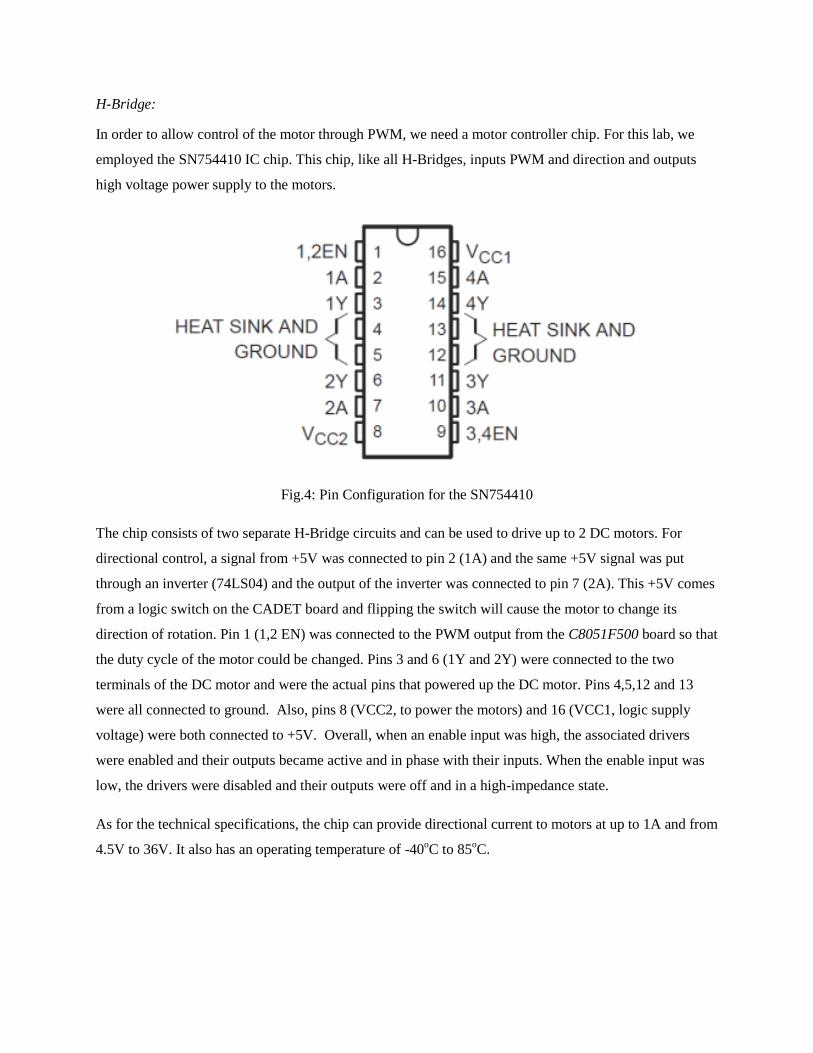
H-Bridge:
In order to allow control of the motor through PWM, we need a motor controller chip. For this lab, we
employed the SN754410 IC chip. This chip, like all H-Bridges, inputs PWM and direction and outputs
high voltage power supply to the motors.
Fig.4: Pin Configuration for the SN754410
The chip consists of two separate H-Bridge circuits and can be used to drive up to 2 DC motors. For
directional control, a signal from +5V was connected to pin 2 (1A) and the same +5V signal was put
through an inverter (74LS04) and the output of the inverter was connected to pin 7 (2A). This +5V comes
from a logic switch on the CADET board and flipping the switch will cause the motor to change its
direction of rotation. Pin 1 (1,2 EN) was connected to the PWM output from the C8051F500 board so that
the duty cycle of the motor could be changed. Pins 3 and 6 (1Y and 2Y) were connected to the two
terminals of the DC motor and were the actual pins that powered up the DC motor. Pins 4,5,12 and 13
were all connected to ground. Also, pins 8 (VCC2, to power the motors) and 16 (VCC1, logic supply
voltage) were both connected to +5V. Overall, when an enable input was high, the associated drivers
were enabled and their outputs became active and in phase with their inputs. When the enable input was
low, the drivers were disabled and their outputs were off and in a high-impedance state.
As for the technical specifications, the chip can provide directional current to motors at up to 1A and from
4.5V to 36V. It also has an operating temperature of -40oC to 85
oC.

Signal Conditioning Circuit:
To interface the encoder from the motor with the C8051F500 board, we would need a signal conditioning
circuit that can be used to detect and remove the non-zero DC offset voltage of the signal. Analog
comparators compare two analog voltage values where one input is typically a reference voltage and the
other the unknown value. When the unknown voltage exceeds the reference, the output of the comparator
switches from one binary state to another. A DC-Level detection comparator circuit was built using the
LM741 op amp. The oscilloscope was used to measure the sine waves from the DC motor and an
appropriate reference voltage was determined for detection.
Parts Needed for Conditioning Circuit: LM741 (Op Amp), 1k Potentiometer to adjust the reference
voltage or a voltage divider as shown in the figure 5.
Fig.5: Signal Conditioning Circuit Used
LCD Display:
Fig.6: Regular 16x2 LCD Display
We made use of the LCD display in this lab to display actual and target RPM of the motor. The LCD that
we used was 16x2, meaning it could display an array of characters that was 16 columns by 2 rows (total
32 characters) as shown in fig 6. The LCD display (CFAH1602A-YYH-JPE) had the following pins:

- Vss : Ground
- Vdd: Supply Voltage (5V)
- VO: Operating voltage for LCD (for adjusting contrast of display through 10K potentiometer)
- RS: Flag, High for Data, Low for Instruction Code, Connected to P3.0
- R/W: High for Read, Low for Write, Connected to P3.1
- E: Chip Enable, Connected to P3.2
- DB0 => DB7: Data Bit 0 to Data Bit 7, where DB7 is also the busy flag, Connected to P2.0 –
P2.7, Where busy flag is P2.7
The operating voltage (VO) for the LCD contrast was connected to a potentiometer circuit to easily adjust
the contrast (brightness of the pixels of the LCD). It was to be noted that if Vo was set too high, there
would be a chance of burning out the LCD display. Also, the grounds of the LCD and the supply line (the
CADET board) were shorted. The LCD interacting circuit that was built on the small CADET board is
given in figure 7.
Fig.7: Wiring Diagram for the 16x2 LCD Display

Software:
For this lab, there were many components that were to be used for the software configuration. Initially,
we had to make sure that the LCD display was working properly. After confirming with working LCD
display, PCA initialization to implement PWM generation, implementation of analog to digital
conversion and pulse-counting using a timer as a counter was configured. Finally, to maintain the same
motor speed when load varies, a stable PID feedback control system was designed and employed to
provide acceptable speed control. While configuring the software, the programs for each part were written
in small step and next part was approached only after making sure that previous part was working
perfectly. The whole software configuration for the system was programmed using C8051F500 board, in
C. The details of each part in given below:
LCD Operation
The LCD consists of two registers – the Instruction Register (IR), to which commands are sent to control
the LCD actions and Data Register (DR), where the display data is sent. The IR can store instructional
codes such as display clear and cursor shift, and address information for display data RAM (DDRAM)
and character generator RAM (CGRAM). Also, the IR can be programmed from the 8051.
Table 1: Register Selection
RS R/W Enable Operation
0 0 H,H -> L IR- write as internal operation
(Display clear, etc.)
0 1 H Read Busy Flag (DB7) and
Address Counter (DB0-DB6)
1 0 H,H -> L DR => write as internal
operation DR to DDRAM or
CG RAM
1 1 H DR-read as internal operation
(DDRAM or CGRAM to DR)
The IR is chosen by setting the Register Select (RS) to ‘0’ and DR with ‘1’. The LCD is also equipped
with a busy flag (DB7). When it is ‘1’, the LCD is in internal operation mode and the next instruction will
not be accepted. As per the Register selection table, the busy flag is output to DB7 when RS = 0 and R/W
= 1. The next instruction cannot be written unless the busy flag is set to ‘0’.

In our program, a function, LCD_Init() was created. In this function, the busy flag was constantly checked
to ensure that the commands are being accepted by the LCD.
Fig. 8: LCD Busy_flag configuration
Within the LCD_Init() function, a sequence of six steps were performed one after the other. In each step,
the enable was set to high and then to low because the internal operations work only when the enable is
high and there is a high to low transition. The six steps of initialization and the pattern of data bus lines
and select bits are shown below in the table.
Table 2: Instructions and Their Corresponding Codes
DB7 DB6 DB5 DB4 DB3 DB2 DB1 DB0 RS R/W E
Clear
Display
0 0 0 0 0 0 0 1 0 0 1->0
Function
Set
0 0 1 1 1 1 0 0 0 0 1->0
Display
Off
0 0 0 0 1 0 0 0 0 0 1->0
Entry
Mode
0 0 0 0 0 1 1 0 0 0 1->0
Display
On
0 0 0 1 1 1 1 1 0 0 1->0
Return
Home
0 0 0 0 0 0 1 0 0 0 1->0
For the checking part, another function,
LCD_busy_flag() was created, which
selected the IR and set the R/W and LCD
Enable to high to read the busy flag from
the IR. The busy flag at line DB7 was read
from P2.7 and returned as an integer
(configured as input).

It is to be noted that before the instructions are executed, the status of the busy flag should be checked so
that it is clear. Given below is the initialization code:
/* --------------------------------------------------
LCD_Init_ISR
setup Timer_0 overflow interrupt service routine
to perform LCD initialization Function
-------------------------------------------------
*/
void LCD_Init_ISR(void) interrupt 1
char SFRPAGE_SAVE = SFRPAGE;
EA = 0;
TH0 = RTH0;
TL0 = RTL0;
EA = 1;
if(LCD_init_flag == 0)
msec_count++;
SFRPAGE = CONFIG_PAGE;
switch(msec_count)
case 5:case 10:case 11:case 12:
//function set four times
LCD_en = 1;
RS = 0;
RW = 0;
P2 = 0x3F;
//Pulse enable
LCD_en = 0;
break;
case 13:
//send display off
LCD_en = 1;
RS = 0;
RW = 0;
P2 = 0x08;
//pulse enable
LCD_en = 0;
break;
case 14:
//send display clear
LCD_en = 1;
RS = 0;
RW = 0;
P2 = 0x01;
//pulse enable
LCD_en = 0;
break;
case 16:
//send entry mode set
LCD_en = 1;
RS = 0;
RW = 0;
P2 = 0x06;
// pulse enable
LCD_en = 0;
break;
case 18:
//send display ON
LCD_en = 1;
RS = 0;
RW = 0;
P2 = 0x0F;
//pulse enable
LCD_en = 0;
//set the LCD_init_flag
LCD_init_flag = 1;
break;
default:
break;
//end of switch-case
//end of if
if(LCD_init_flag == 1)
SFRPAGE = ACTIVE_PAGE;
TR0 = 0; //disable Timer_0 overflow interrupt, LCD is
initailized
ET0 = 0;
//end of if
SFRPAGE = SFRPAGE_SAVE;
//LCD_Init()

Fig. 9: LCD initialization Function using timer 0 overflow interrupt
After the initialization was complete, the LCD needed to be setup for writing. For our application
purposes, we were only writing to the data lines. For displaying, the LCD needs to be refreshed
constantly to update the display. The refreshing was achieved by using Timer 1 Overflow
Interrupt and the advised refresh rate was 50Hz. We also needed to specify the cursor to move to
the next line when the 16th
character was reached in a row. When the 32nd
character was
displayed, the LCD was instructed to return to the home position. The position of this cursor was
monitored using a LCD_pointer variable.
Fig.10: The LCD Display Refresh Function
For the actual display of the text, we implemented the following numeric to character data type
function:

Fig. 11: Numeric to Character Data Type Function
As we can see above in figure 11, the TARGET RPM and ACTUAL in RPM were assigned as
four bit signed decimal numbers. In the part of the program with those numbers, we can see the
conversion of numeric data type to character data type.

PWM Generation using Programmable Counter Array (PCA)
PWN is used to control the duty cycle of a square wave, varying between 0% to 100%, and provides the
necessary flexibility for many application. In this lab, the SiliconLab-C8051F500 is being employed to
generate the appropriate PWM signal to control motor rotation speed. The PWM output is connected
directly to an intelligent PWM control H-Bridge chip that will translate the duty cycle information to
drive the DC motor accordingly.
In order to this, C8051F500 provides a Programmable Counter Array (PCA0) consisting of a dedicated
16-bit counter/timer and six 16-bit capture/compare modules. Each capture/compare module has its own
associated I/O line (CEXn), which is routed through the crossbar to port I/O when enabled. For this lab,
we were using capture/compare module 0, where CEX0 was used to generate PWM pulses, while PCA0
timer was driven by the system clock divided by 12. The mode of the PWM was set to 8-bit pulses. Thus,
when the value in the low byte of the PCA counter/timer (PCA0L) was equal to the value in PCA0CPL0,
the PWM signal switches to high and the output on the CEX0 pin will be set. When the count value in
PCA0L overflows, the CEX0 output will be reset. This process will repeat to generate PWM signal with
intended duty cycle. The duty cycle of PWM signal was modulated by changing the value stored in
PCA0CPL0 register as shown:
Setting ECOM0 and PWM0 bits in the PCA0CPM0 register, and setting CLSEL bits in register PCA0PWM to
00b, 8-Bit Pulse Width Modulator mode was enabled using configuration wizard as shown in fig. 12.
Fig. 12: PCA initialization to generate PWM
Initially, the internal oscillator frequency was set at 750000 and we were still able to generate the PWM
pulses. After measuring the frequency of the PWM signal in oscilloscope, we found it to be ~245 Hz.
However, according to Prof. Ning’s instructions, the H-bridge works best at PWM signal frequency of 1
KHz. Thus, internal oscillator frequency was set to 3 MHz using configuration wizard.

Fig.13: Oscillator Initialization with SYSCLK of 3MHz
As soon as clock was changed from the 0.75MHz to 3 MHz, the LCD display started acting weird as
expected as it was not getting enough time to settle down. Thus, we increased the setting time for the
LCD display refreshing from 25 TIMER-1 overflow interrupts to 100 TIMER-1 overflow interrupts, as
the clock was also changed by a factor of 4.
Hence, in the LCD display refresh function, this part :
was changed to:
However, it was still unable to get to the best condition. Thus, we decided to create same delay in the
LCD Busy_flag function, (fig, 14) which did the trick for us to bring the LCD was back to normal.
Fig. 14: Adding a delay to let LED settle before going to to original position

Analog-Digital Conversion:
As specified in the design contains, the most important design goal of this lab was to Allow the users to
easily adjust the desired motor rpm speed. In order to do so, A/D converter (ADC0 for 12-bit A/D) on the
Silicon-Lab C8051F500 microcontroller was used. The ADC0 on the C8051F50x/F51x consists of an
analog multiplexer (AMUX0) with 35/28 total input selections and a 200 kilo-samples-per-second (ksps),
12-bit successive-approximation-register (SAR) ADC with integrated track-and-hold, programmable
window detector, programmable attenuation (1:2), and hardware accumulator.
In order to initiate the conversion, we chose TIMER 2 overflow interrupt as repeated A/D conversions
can be achieved in fixed intervals. Fig. 12 shows the configuration of TIMER 2 interrupt:
Fig 12: Timer 2 overflow interrupt used to initiate A/D conversion
The conversion mode is determined by the programmed states of the ADC0 bits (AD0CM1, AD0CM0) in
bit-adorable SFR ADC0CN. ADC0CN was set to 11, representing the conversion initialization to TIMER
2 overflow interrupt. AD0BUSY bit in the ADC0CN SFR was set to 1 during conversion and cleared
when conversion complete. The falling edge of the AD0BUSY bit triggers an interrupt and sets the
ADOINT interrupt flag. The converted data then become available in the ADC0H and ADC0L. Output in
our case is right-justified in our case, so the most significant 8 bits of the converted data would reside in
ADC0L and ADC0H would carry the least significant 4 bits.
While configuring ADC0, the example program from the Silicon-Lab library proved to be very helpful.
ADC0 on the C8051F500 implements a selectable gain adjustment option because input sources have
small part-to-part variations that must be accounted for to achieve accurate results and the programmable
gain value could be used as a calibration value to eliminate these part-to-part variations. Thus, gain was
initialized to account for a 5V input and Vref was set to ground. The gain value was calculated using the
following formula, which is represented as a 12-bit frame ranging from 0x000 to 0Xfff.

The gain enable bit [ADC0CF.0] was set and ADC0H were loaded with ADC0GNH, ADC0GNL, or
ADC0GNA addresses. As mentioned earlier, ADC0L was then loaded with the upper bytes GAIN value,
which is 0x6C in this case. However, an ADC conversion should not be performed while the GAINEN bit is set.
Thus the gain bit is set to 0 after proper configuration. ADC0 is then disabled and normal tracking conversion is triggered on
TIMER 2 overflow interrupt by setting ADC0CN to 0x03. P1.2 is used as the analog input pin and ADC0 conversion complete
interrupt was enabled by setting EIE1 to 0x04 and AD0EN to 1. The detailed code is given in fig. 13.
Fig. 13: Analog-digital conversion configuration using A/D converter
Pulse-Counting of actual RPM signal:

In order to find the actual RPM of running DC motor, the pulse counts per second is required to
be measured. In order to measure the pulses, we needed to use a timer that can be used as a counter.
However, as described already, all four timers were already being used. Then we realized that we are not
using TIMER 0 after the LCD display is initialized once. Thus, we decided use TIMER 0 after the LCD
display initialization was completed to count the pulses generated. In order to measure the current RPM
of the motor, we configured Timer 0 as an 8 bit auto-reload counter. In the configuration wizard, we set
T0 to P0.3 in order to record the number of pulses. The pulses, as explained earlier, could not be directly
used by the C8051F120, therefore we had to send the signal through the comparator circuit. The output of
the comparator circuit was then sent to the C8051F120 in order to count the pulses. While loading the
TIMER 2 overflow values, we had to take care of internal oscillator frequency. As mentioned earlier, the
internal oscillator clock used in this system was 3MHz. Thus, when we were loading the values for the
auto-reload mode, we had to make sure that they were properly calculated. The TIMER-2 was configured
as SYSCLK/12, so I took 4 μs (1/(3000000/12)) for one machine cycle. Thus, when we trying to measure
pulse-counts per 100 ms, actual delay was supposed to be (100 ms/4) = 25 ms. Hence, (65535-25000 =
40535) 10 = (9E57)16 was loaded in the TIMER-2 registers as shown in the fig. 14.
else if(LCD_init_flag == 1)
EA = 0;
TMR3CN = 0x04; //Start running Timer 3
TMOD = 0x15; //Timer_0 set as event counter and Timer_1 still in 16-bit mode
TH0 = 0x00; //Timer 0 high and low bytes set
TL0 = 0x00;
ET0 = 0; //Disable Timer 0 interrupt, Timer 0 will now be used to count pulses
EIE1 |= 0x40; //Timer 3 interrupt enabled and used to record pulses counted by Timer0
TMR3L= 0x57; //Timer 3 high and low bytes set to record pulse every 100 msec
TMR3H = 0x9E;
TMR3RLL = 0x57; //Timer 3 auto reload values set
TMR3RLH = 0x9E;
EA = 1;
Fig. 14: Configuration of TIMER 0 and TIMER 2 overflow interrupt
After configuring TIMER 0 as a counter to count pulses and TIMER 3 overflow interrupt to record the
counted pulses, which is equal to (total_pulse_count = TH0*256 + TL0). The total_pulse_count is then
used to measure the actual speed of the running DC motor in rpm using the following formula.
where total_pulse_count is in x-msec.
As suggested by prof. Ning, mechanical devices like DC motor is not fast enough to adjust the speed in
very small time frame like 100 msec. Thus, we decided to record the pulses after 500 ms or ½ second. A
small counter was used to count the 100 ms delay set by TIMER 3 overflow interrupt and after such 5
interrupt, total_pulses_counts were recorded using the above equation.
However, after trying multiple combinations of TIMER-3 overflow delay, we were not getting the result
expected. Then we decided to measure the frequency of the pulses recorded and we noticed the counter in
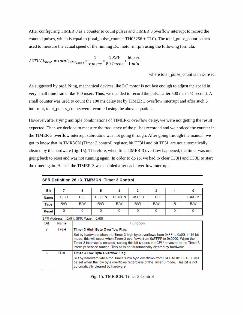
the TIMER-3 overflow interrupt subroutine was not going through. After going through the manual, we
got to know that in TMR3CN (Timer 3 control) register, bit TF3H and bit TF3L are not automatically
cleared by the hardware (fig. 15). Therefore, when first TIMER-3 overflow happened, the timer was not
going back to reset and was not running again. In order to do so, we had to clear TF3H and TF3L to start
the timer again. Hence, the TIMER-3 was enabled after each overflow interrupt.
Fig. 15: TMR3CN: Timer 3 Control

After enabling TIMER-3 again in TIMER-3 overflow interrupt subroutine, we were getting the results
expected. However, though we were getting better result, the values were still fluctuating so much. Thus,
we decided to record the pulses after 1000ms or 1 second. Therefore, after 10 TIMER-2 overflow
interrupts (each with 100ms), total_pulses_counts were recorded and used to find current speed of motor
in rpm as shown in following equation. Fig. 16 gives details about TIMER-3 overflow interrupt
subroutine.
----------------------------------------------------------
Timer2_Overflow_ISR
The Routine will count the number of pulses. The number
of pulses comes from TL0 and TH0 because Timer 0 was set to
record pulses
----------------------------------------------------------
*/
void Timer3_Overflow_ISR(void) interrupt 13 //Interrupts every 100msec (auto reload)
TMR3CN = 0x04; //Timer-3 is enabled again
ISRT3_count++;
if (ISRT3_count == 10) //refreshes actual_rpm every 100*10 = 1000 msec
pulse_count = TH0*256 + TL0; // the number of pulses
TH0 = 0x00; //Timer 0 high and low bytes reset
TL0 = 0x00;
//Routine convert pulses into RPM here
//rpm = pulse_count(1/1000msec)(1000msec/1sec)(60sec/1min)(1turn/80counts)
actual_rpm = pulse_count * 0.75;
ISRT3_count = 0;
target_rpm = ADC0;
FEEDBACK_Init();
Fig. 16: Timer -3 Overflow Interrupt Service Routine

After configuring the LCD display, PWM generation using Programmable Counter Array (PCA), desired
speed target using A/D converter and calculating the actual rpm, everything was placed together to check
the whole embedded system. We were able to change the desired target speed and thus, the actual speed
of the motor. The change in the target speed and actual speed was successfully displaced on the LCD
display. However, there was no proper correlation between the desired target speed and actual speed. In
order to adjust the PWM signal to achieve a desired target speed a feedback controller was necessary.
Thus, feedback control was designed using the difference between the desired target speed and the actual
speed of the motor. Thus, when the desired target speed was different than the actual speed, duty cycle of
the PWM signal was adjusted accordingly by the controller to maintain the desired speed. When target
speed was higher than actual speed of the motor, duty cycle of PWM signal was increased accordingly by
decreasing the value of PCA0CPH0 in programmable counter array (PCA) and vice versa.
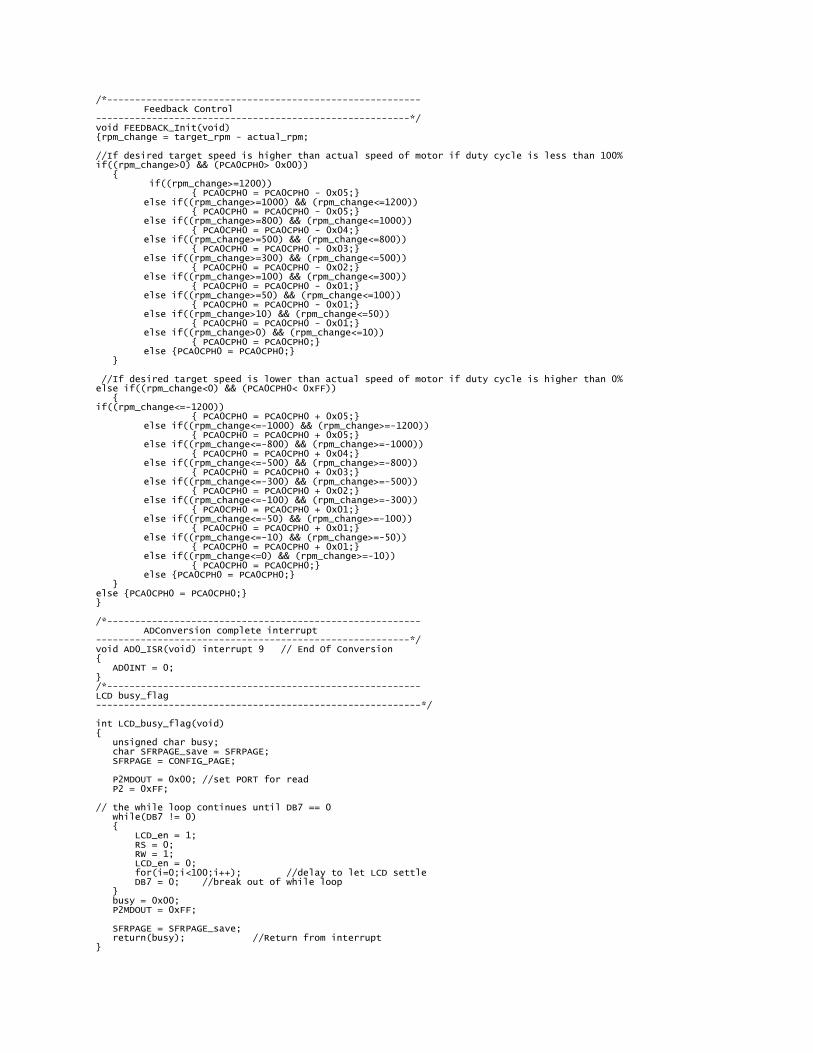
/*-------------------------------------------------------- Feedback --------------------------------------------------------*/ void FEEDBACK_Init(void)
rpm_change = target_rpm - actual_rpm
if(rpm_change > 0 && PCA0CPH0 > 0x05)
PCA0CPH0 = PCA0CPH0 - 0x01;
else if(rpm_change < 0 && PCA0CPH0<0xFF)
PCA0CPH0 = PCA0CPH0 + 0x01;
Else PCA0CPH0 = PCA0CPH0;
Fig. 17: Initial approach to control the
Initially we wrote a simple program (fig. 17), which will increase duty cycle if the difference between
desired target speed and actual speed is higher than 0 and will decrease the duty cycle if difference
between desired target speed and actual speed is less than zero given that the duty cycle is between 0%
and 100%. However, the feedback was not responsive enough and it took so long for the actual speed to
adjust accordingly to the target speed. Furthermore, when we tried to change the incrementing value of
PCA capture module 0 high byte (PCA0CPH0), the actual speed started fluctuating. Thus, we decided to
keep checking the difference between target rpm and actual rpm constantly and then change the value of
PCA0CPH0 accordingly. The difference between target rpm and actual rpm was being checked from 0 to
±1200 and appropriate change in PCA0CPH0 was placed. After employing the change in the feedback
control loop, our motor started adjusting the actual speed very quickly according the desired target speed.
In addition, by removing the load or increasing the load, the duty cycle was quickly being automatically
adjusted accordingly by the controller to maintain the desired speed. Furthermore, the actual speed was
not fluctuating and will stay within ±15-20 rpm of target speed. This was also verified from the stable
actual speed in rpm and PWM signal from the oscilloscope. The final working code for the feedback
control is given in fig. 18.

/*-------------------------------------------------------- Feedback Control --------------------------------------------------------*/ void FEEDBACK_Init(void)
rpm_change = target_rpm - actual_rpm;
//If desired target speed is higher than actual speed of motor if duty cycle is less than 100%
if((rpm_change>0) && (PCA0CPH0> 0x00))
if((rpm_change>=1200))
PCA0CPH0 = PCA0CPH0 - 0x05;
else if((rpm_change>=1000) && (rpm_change<=1200))
PCA0CPH0 = PCA0CPH0 - 0x05;
else if((rpm_change>=800) && (rpm_change<=1000))
PCA0CPH0 = PCA0CPH0 - 0x04;
else if((rpm_change>=500) && (rpm_change<=800))
PCA0CPH0 = PCA0CPH0 - 0x03;
else if((rpm_change>=300) && (rpm_change<=500))
PCA0CPH0 = PCA0CPH0 - 0x02;
else if((rpm_change>=100) && (rpm_change<=300))
PCA0CPH0 = PCA0CPH0 - 0x01;
else if((rpm_change>=50) && (rpm_change<=100))
PCA0CPH0 = PCA0CPH0 - 0x01;
else if((rpm_change>10) && (rpm_change<=50))
PCA0CPH0 = PCA0CPH0 - 0x01;
else if((rpm_change>0) && (rpm_change<=10))
PCA0CPH0 = PCA0CPH0;
else PCA0CPH0 = PCA0CPH0;
//If desired target speed is lower than actual speed of motor if duty cycle is higher than 0%
else if((rpm_change<0) && (PCA0CPH0< 0xFF))
if((rpm_change<=-1200))
PCA0CPH0 = PCA0CPH0 + 0x05;
else if((rpm_change<=-1000) && (rpm_change>=-1200))
PCA0CPH0 = PCA0CPH0 + 0x05;
else if((rpm_change<=-800) && (rpm_change>=-1000))
PCA0CPH0 = PCA0CPH0 + 0x04;
else if((rpm_change<=-500) && (rpm_change>=-800))
PCA0CPH0 = PCA0CPH0 + 0x03;
else if((rpm_change<=-300) && (rpm_change>=-500))
PCA0CPH0 = PCA0CPH0 + 0x02;
else if((rpm_change<=-100) && (rpm_change>=-300))
PCA0CPH0 = PCA0CPH0 + 0x01;
else if((rpm_change<=-50) && (rpm_change>=-100))
PCA0CPH0 = PCA0CPH0 + 0x01;
else if((rpm_change<=-10) && (rpm_change>=-50))
PCA0CPH0 = PCA0CPH0 + 0x01;
else if((rpm_change<=0) && (rpm_change>=-10))
PCA0CPH0 = PCA0CPH0;
else PCA0CPH0 = PCA0CPH0;
else PCA0CPH0 = PCA0CPH0;
Fig. 18: Feedback control loop to adjust actual speed according to desired target speed

Implementation
As mentioned already, there were many components that were to be employed for the hardware as well as
software configuration. Thus, while configuring the whole system, each part was configured in small step
and next part was approached only after making sure that previous part was working perfectly. Initially,
given LCD display was properly wired using the wiring diagram given in fig.7. It was a good advantage
for us that an almost working code for the LCD was provided. Modifying the code a bit, we were able to
make our LCD display desired output. While I was working on the programming, Bicky finished building
the circuitry consisting of H-bridge, DC motor with optical encoder, comparator, inverter and op-amp.
With the LCD screen working with one set of code, we referenced the PWM example code given in the
lab handout. This helped us to set up PCA and to generate varying duty cycles of the PWM. Before we
hooked up the H-Bridge, we connected the PCA directly to the Port 0.2 (CEX0), which was configured
using the configuration wizard. In order to obtain a stable PWN signal, we needed to measure the actual
speed of the DC motor. Thus, timer 0 was configured as 16-bit counter while timer-3 overflow interrupt
was used for count the pulses measured by counter 0. However, the pulses we obtained from the PWM
were not being counted by Timer 0. To increase the current of the PWM pulses, we passed the output of
the comparator through a buffer. This solved the problem and enabled the timer to count the pulses.
Working with the PWM code, we then passed the PWM to the input of the H-Bridge to power the motor.
When we connected the pulses from the motor to the oscilloscope, we were able to get expected signal.
The desired rpm speed was then set using the Analog to Digital Converter with help of example code
given in the SILABs documentation. We used GND as reference voltage for VREF (P0.0). Using the
value of total-pulses obtained using counter 0 and TIMER-3 overflow interrupt, actual rotating spped was
found. Using actual and target speed, feedback control loop was finally employed to adjust actual speed
of the motor accordingly to the desired target speed. Multiple tests were performed to design the best
possible feedback control system.
When we thought we were almost done one week ago, we decided to check the progress with professor.
Then we realized that the H-bridge works best with the oscillator frequency that leads to the PWM signal
frequency of 1KHz. Hence, we had to change our clock from 0.75 MHz to 3 Mhz. This change brought us
back to the same place where we started. Nothing including LCD display, actual-rpm courting or
feedback-control was working. Three-four days were spent without any significant progress. However,
things started to be on track after we figured out the timing conflict with the delays in the timer overflow
interrupt due to the change in oscillator. After multiple tests with different values of almost every single
variable, the DC motor speed control embedded system was finalized.

Results and Discussion
As per the design goal of the lab, we were able to construct DC-motor based embedded system, where
PID feedback controller was designed that would allow the user to enter the desired target speed and
timely adjustment to the PWM would be made to accommodate the changing shaft-load to maintain the
desired rotating speed. As mentioned above in the fig.17, while demonstrating the lab to professor, the
feedback control was designed to slowly adjust the actual rotating speed of the motor according to desired
target speed. However, after the professor’s concern, we implemented the feedback using the code given
in fig.18, which was able to make quick adjustment in the actual rotating speed according to the target
speed when load was applied.
This lab opened the doors for what we can do with the 8051-based microcontrollers. While learning about
the Automatic Control System (ACS), I never thought that I could even use it literally. However, this lab
demonstrated practical ways of implementing closed-loop feedback systems. Furthermore, this lab also
helped a lot to improve our command on C/C++ language.
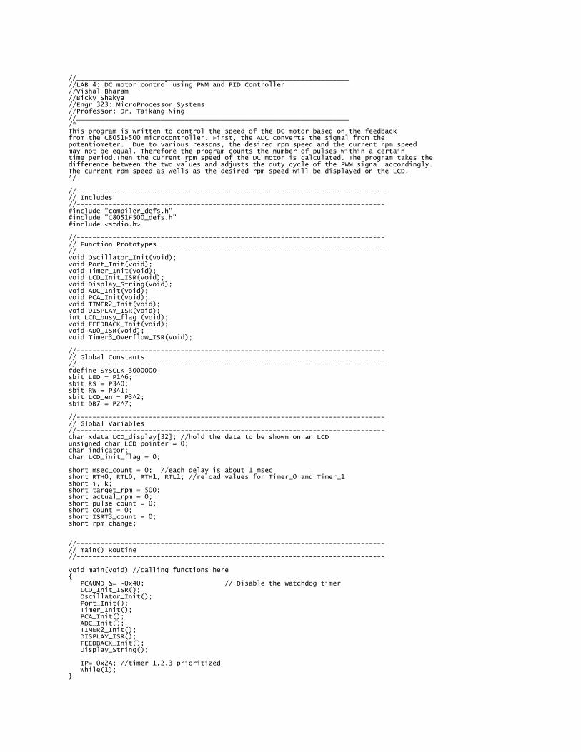
//____________________________________________________________________ //LAB 4: DC motor control using PWM and PID Controller //Vishal Bharam //Bicky Shakya //Engr 323: MicroProcessor Systems //Professor: Dr. Taikang Ning //____________________________________________________________________ /* This program is written to control the speed of the DC motor based on the feedback from the C8051F500 microcontroller. First, the ADC converts the signal from the potentiometer. Due to various reasons, the desired rpm speed and the current rpm speed may not be equal. Therefore the program counts the number of pulses within a certain time period.Then the current rpm speed of the DC motor is calculated. The program takes the difference between the two values and adjusts the duty cycle of the PWM signal accordingly. The current rpm speed as wells as the desired rpm speed will be displayed on the LCD. */ //----------------------------------------------------------------------------- // Includes //----------------------------------------------------------------------------- #include "compiler_defs.h" #include "C8051F500_defs.h" #include <stdio.h> //----------------------------------------------------------------------------- // Function Prototypes //----------------------------------------------------------------------------- void Oscillator_Init(void); void Port_Init(void); void Timer_Init(void); void LCD_Init_ISR(void); void Display_String(void); void ADC_Init(void); void PCA_Init(void); void TIMER2_Init(void); void DISPLAY_ISR(void); int LCD_busy_flag (void); void FEEDBACK_Init(void); void AD0_ISR(void); void Timer3_Overflow_ISR(void); //----------------------------------------------------------------------------- // Global Constants //----------------------------------------------------------------------------- #define SYSCLK 3000000 sbit LED = P1^6; sbit RS = P3^0; sbit RW = P3^1; sbit LCD_en = P3^2; sbit DB7 = P2^7; //----------------------------------------------------------------------------- // Global Variables //----------------------------------------------------------------------------- char xdata LCD_display[32]; //hold the data to be shown on an LCD unsigned char LCD_pointer = 0; char indicator; char LCD_init_flag = 0; short msec_count = 0; //each delay is about 1 msec short RTH0, RTL0, RTH1, RTL1; //reload values for Timer_0 and Timer_1 short i, k; short target_rpm = 500; short actual_rpm = 0; short pulse_count = 0; short count = 0; short ISRT3_count = 0; short rpm_change; //----------------------------------------------------------------------------- // main() Routine //----------------------------------------------------------------------------- void main(void) //calling functions here PCA0MD &= ~0x40; // Disable the watchdog timer LCD_Init_ISR(); Oscillator_Init(); Port_Init(); Timer_Init(); PCA_Init(); ADC_Init(); TIMER2_Init(); DISPLAY_ISR(); FEEDBACK_Init(); Display_String(); IP= 0x2A; //timer 1,2,3 prioritized while(1);

//----------------------------------------------------------------------------- // Initialization Subroutines //----------------------------------------------------------------------------- /*-------------------------------- Oscillator_Init This routine initializes the system clock to use the precision internal oscillator as its clock source --------------------------------------------------- */ void Oscillator_Init(void) SFRPAGE = CONFIG_PAGE; OSCICN = 0xC4; //Select the internal oscillator as system clock 12.25 MHz CLKSEL = 0x00; //Select the internal oscillator as SYSCLK source SFRPAGE = ACTIVE_PAGE; /*------------------------------------------------------- PORT_Init() -------------------------------------------------------*/ void Port_Init(void) char SFRPAGE_SAVE = SFRPAGE; SFRPAGE = CONFIG_PAGE; P0SKIP |= 0x03; // Skip P0.0 (VREF) P0MDIN = 0xFC; P0MDOUT = 0x0C; // Set External Timer 0 (P0.0) to push-pull XBR1= 0x44; //CEX0 at port0.2, timer0 pin at p0.1 P1SKIP |= 0x04; // Skip P1.2 (ADC input) P1MDIN &= ~0x04; // Set P1.2 as an analog input P1MDOUT |= 0x08; //P1.6(LED) P3MDOUT = 0x07; //LCD-en(P6.2) RS(P6.0) and RW(P6.1) are set P2MDOUT = 0xFF; //DB0-DB7 are set push-pull XBR2 = 0x40; //Enable Crossbar SFRPAGE = SFRPAGE_SAVE; //----------------------------------------------------------------------------- // TIMER2_Init //----------------------------------------------------------------------------- // // Return Value: None // Parameters: None // // Configure Timer2 to 16-bit auto-reload and generate an interrupt at 100uS // intervals. Timer 2 overflow automatically triggers ADC0 conversion. // //----------------------------------------------------------------------------- void TIMER2_Init (void) U8 SFRPAGE_save = SFRPAGE; SFRPAGE = ACTIVE_PAGE; TMR2CN = 0x00; // Stop Timer2; Clear TF2; // use SYSCLK as timebase, 16-bit auto-reload TMR2RL = 65535 - (SYSCLK / 10000); // Init reload value for 10uS TMR2 = 0xFFFF; // Set to reload immediately TR2 = 1; // Start Timer2 SFRPAGE = SFRPAGE_save; //----------------------------------------------------------------------------- //----------------------------------------------------------------------------- // ADC_Init //----------------------------------------------------------------------------- // // Return Value: None // Parameters: None // // Configures ADC0 to make single-ended analog measurements on pin P1.2 // Also enabled the gain and the voltage reference // //----------------------------------------------------------------------------- void ADC_Init() U8 SFRPAGE_save = SFRPAGE; SFRPAGE = ACTIVE_PAGE; // Initialize the Gain to account for a 5V input and 2.25 VREF // Solve the equation provided in Section 9.3.1 of the Datasheet

// The 5V input is scaled by a factor of 0.44 so that the maximum input // voltage seen by the pin is 2.2V // 0.44 = (GAIN/4096) + GAINADD * (1/64) // Set GAIN to 0x6CA and GAINADD to 1 // GAIN = is the 12-bit word formed by ADC0GNH[7:0] ADC0GNL[7:4] // GAINADD is bit ADC0GNA.0 ADC0CF |= 0x01; // Set GAINEN = 1 ADC0H = 0x04; // Load the ADC0GNH address ADC0L = 0x6C; // Load the upper byte of 0x6CA to // ADC0GNH ADC0H = 0x07; // Load the ADC0GNL address ADC0L = 0xA0; // Load the lower nibble of 0x6CA to // ADC0GNL ADC0H = 0x08; // Load the ADC0GNA address ADC0L = 0x01; // Set the GAINADD bit ADC0CF &= ~0x01; // Set GAINEN = 0 ADC0CN = 0x03; // ADC0 disabled, normal tracking, // conversion triggered on TMR2 overflow // Output is right-justified REF0CN = 0x33; // Enable on-chip VREF and buffer // Set voltage reference to GND ADC0MX = 0x0A; // Set ADC input to P1.2 ADC0CF = ((SYSCLK / 3000000) - 1) << 3; // Set SAR clock to 3MHz EIE1 |= 0x04; // Enable ADC0 conversion complete int. AD0EN = 1; // Enable ADC0 SFRPAGE = SFRPAGE_save; /*---------------------------------------------------- Timer_Init(); set Timer_0 and Timer_1 as 16 bit ----------------------------------------------------- */ void Timer_Init(void) char SFRPAGE_SAVE = SFRPAGE; SFRPAGE = ACTIVE_PAGE; TMOD = 0x11; //Timer_0 and Timer_1 in 16-bit mode RTL0 = 0x17; //1000 cycles for about 1 msec RTH0 = 0xFC; TR0 = 1; ET0 = 1; RTL1 = 0x77; //refresh rate of 100Hz (10 msec) RTH1 = 0xF8; TR1 = 1; ET1 = 1; EA = 1; //EA and TF0,TF1, and EA are enabled SFRPAGE = SFRPAGE_SAVE; /*------------------------------------------------------ PWM COUNTER ------------------------------------------------------*/ void PCA_Init(void) PCA0CN = 0x40; PCA0CPM0 = 0x42; PCA0CPH0 = 0x80; /* -------------------------------------------------- LCD_Init_ISR setup Timer_0 overflow interrupt service routine to perform LCD initialization Function -------------------------------------------------*/ void LCD_Init_ISR(void) interrupt 1 if(LCD_init_flag == 0) EA = 0; TH0 = RTH0; TL0 = RTL0; EA = 1;

msec_count++; switch(msec_count) case 5:case 10:case 11:case 12: //function set four times LCD_en = 1; RS = 0; RW = 0; P2 = 0x3F; // pulse enable LCD_en = 0; break; case 13: //send display off LCD_en = 1; RS = 0; RW = 0; P2 = 0x08; //pulse enable LCD_en = 0; break; case 14: //send display clear LCD_en = 1; RS = 0; P2 = 0x01; //pulse enable LCD_en = 0; break; case 16: //send entry mode set LCD_en = 1; RS = 0; RW = 0; P2 = 0x06; //pulse enable LCD_en = 0; break; case 18: //send display ON LCD_en = 1; RS = 0; RW = 0; P2 = 0x0F; //pulse enable LCD_en = 0; //set the LCD_init_flag LCD_init_flag = 1; break; default: break; //end of switch-case //end of if else if(LCD_init_flag == 1) EA = 0; TMR3CN = 0x04; //Start running Timer 2 TMOD = 0x15; //Timer_0 set as event counter and Timer_1 still in 16-bit mode TH0 = 0x00; //Timer 0 high and low bytes set TL0 = 0x00; ET0 = 0; //Disable Timer 0 interrupt, Timer 0 will now be used to count pulses and Timer 2 records EIE1 |= 0x40; //Timer 2 interrupt enabled TMR3L = 0x57; //Timer 2 high and low bytes set to record pulse count every 5 msec TMR3H = 0x9E; TMR3RLL = 0x57; //Timer 2 auto reload values set TMR3RLH = 0x9E; EA = 1; // SFRPAGE = SFRPAGE_SAVE; //LCD_Init()

/* --------------------------------------------------- LCD Display Refresh Function --------------------------------------------------- */ void DISPLAY_ISR(void) interrupt 3 //EA = 0; TL1 = RTL1; //Refresh rate of 50Hz TH1 = RTH1; //20-msec interval Display_String(); //The program will not refresh the LCD until the intialization is complete if((LCD_init_flag == 1) && (LCD_busy_flag() == 0)) switch(LCD_pointer) case 16: LCD_en = 1; RS = 0; RW = 0; P2 = 0xC0; //set DD RAM address to 40H (A7 = 1 100 0000) LCD_en = 0; for(k=0;k<100;k++); //delay to let LCD settle break; case 32: LCD_en = 1; RS = 0; RW = 0; P2 = 0x02; //move cursor to home position LCD_en = 0; LCD_pointer = 0; for(k=0;k<100;k++); //delay to let LCD settle break; default: break; //end of switch //Display the LCD data LCD_en = 1; RS = 1; RW = 0; P2 = LCD_display[LCD_pointer]; LCD_en = 0; LED = ~LED; LCD_pointer++; /* ---------------------------------------------------------- Timer2_Overflow_ISR The Routine will count the number of pulses. The number of pulses comes from TL0 and TH0 because Timer 0 was set to record pulses ---------------------------------------------------------- */ void Timer3_Overflow_ISR(void) interrupt 13 //Interrupts every 5 msec and auto reload TMR3CN = 0x04; ISRT3_count++; if (ISRT3_count == 10) //refreshes actual_rpm every 1000 msec pulse_count = TH0*256 + TL0; // the number of pulses TH0 = 0x00; //Timer 0 high and low bytes reset TL0 = 0x00; //Routine convert pulses into RPM here //rpm = pulse_count(1/1000msec)(1000msec/1sec)(60sec/1min)(1turn/80counts) actual_rpm = pulse_count * 0.75; ISRT3_count = 0; target_rpm = ADC0; FEEDBACK_Init();
/*-------------------------------------------------------- Feedback Control --------------------------------------------------------*/ void FEEDBACK_Init(void) rpm_change = target_rpm - actual_rpm; //If desired target speed is higher than actual speed of motor if duty cycle is less than 100% if((rpm_change>0) && (PCA0CPH0> 0x00)) if((rpm_change>=1200)) PCA0CPH0 = PCA0CPH0 - 0x05; else if((rpm_change>=1000) && (rpm_change<=1200)) PCA0CPH0 = PCA0CPH0 - 0x05; else if((rpm_change>=800) && (rpm_change<=1000)) PCA0CPH0 = PCA0CPH0 - 0x04; else if((rpm_change>=500) && (rpm_change<=800)) PCA0CPH0 = PCA0CPH0 - 0x03; else if((rpm_change>=300) && (rpm_change<=500)) PCA0CPH0 = PCA0CPH0 - 0x02; else if((rpm_change>=100) && (rpm_change<=300)) PCA0CPH0 = PCA0CPH0 - 0x01; else if((rpm_change>=50) && (rpm_change<=100)) PCA0CPH0 = PCA0CPH0 - 0x01; else if((rpm_change>10) && (rpm_change<=50)) PCA0CPH0 = PCA0CPH0 - 0x01; else if((rpm_change>0) && (rpm_change<=10)) PCA0CPH0 = PCA0CPH0; else PCA0CPH0 = PCA0CPH0; //If desired target speed is lower than actual speed of motor if duty cycle is higher than 0% else if((rpm_change<0) && (PCA0CPH0< 0xFF)) if((rpm_change<=-1200)) PCA0CPH0 = PCA0CPH0 + 0x05; else if((rpm_change<=-1000) && (rpm_change>=-1200)) PCA0CPH0 = PCA0CPH0 + 0x05; else if((rpm_change<=-800) && (rpm_change>=-1000)) PCA0CPH0 = PCA0CPH0 + 0x04; else if((rpm_change<=-500) && (rpm_change>=-800)) PCA0CPH0 = PCA0CPH0 + 0x03; else if((rpm_change<=-300) && (rpm_change>=-500)) PCA0CPH0 = PCA0CPH0 + 0x02; else if((rpm_change<=-100) && (rpm_change>=-300)) PCA0CPH0 = PCA0CPH0 + 0x01; else if((rpm_change<=-50) && (rpm_change>=-100)) PCA0CPH0 = PCA0CPH0 + 0x01; else if((rpm_change<=-10) && (rpm_change>=-50)) PCA0CPH0 = PCA0CPH0 + 0x01; else if((rpm_change<=0) && (rpm_change>=-10)) PCA0CPH0 = PCA0CPH0; else PCA0CPH0 = PCA0CPH0; else PCA0CPH0 = PCA0CPH0; /*-------------------------------------------------------- ADConversion complete interrupt --------------------------------------------------------*/ void AD0_ISR(void) interrupt 9 // End Of Conversion AD0INT = 0; /*-------------------------------------------------------- LCD busy_flag ----------------------------------------------------------*/ int LCD_busy_flag(void) unsigned char busy; char SFRPAGE_save = SFRPAGE; SFRPAGE = CONFIG_PAGE; P2MDOUT = 0x00; //set PORT for read P2 = 0xFF; // the while loop continues until DB7 == 0 while(DB7 != 0) LCD_en = 1; RS = 0; RW = 1; LCD_en = 0; for(i=0;i<100;i++); //delay to let LCD settle DB7 = 0; //break out of while loop busy = 0x00; P2MDOUT = 0xFF; SFRPAGE = SFRPAGE_save; return(busy); //Return from interrupt
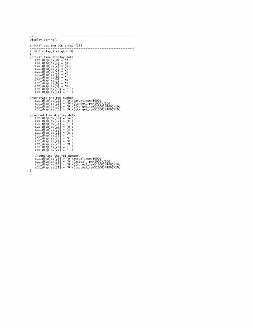
/*---------------------------------------------------------- Display_String() Initializes the LCD array [32] ----------------------------------------------------------*/ void Display_String(void) //first line display data LCD_display[0] = 'T'; LCD_display[1] = 'A'; LCD_display[2] = 'R'; LCD_display[3] = 'G'; LCD_display[4] = 'E'; LCD_display[5] = 'T'; LCD_display[6] = ' '; LCD_display[7] = 'R'; LCD_display[8] = 'P'; LCD_display[9] = 'M'; LCD_display[10] = '-'; LCD_display[11] = ' '; //generate the rpm number LCD_display[12] = '0'+target_rpm/1000; LCD_display[13] = '0'+(target_rpm%1000)/100; LCD_display[14] = '0'+((target_rpm%1000)%100)/10; LCD_display[15] = '0'+((target_rpm%1000)%100)%10; //second line display data LCD_display[16] = 'A'; LCD_display[17] = 'C'; LCD_display[18] = 'T'; LCD_display[19] = 'U'; LCD_display[20] = 'A'; LCD_display[21] = 'L'; LCD_display[22] = ' '; LCD_display[23] = 'R'; LCD_display[24] = 'P'; LCD_display[25] = 'M'; LCD_display[26] = '-'; LCD_display[27] = ' '; //generate the rpm number LCD_display[28] = '0'+actual_rpm/1000; LCD_display[29] = '0'+(actual_rpm%1000)/100; LCD_display[30] = '0'+((actual_rpm%1000)%100)/10; LCD_display[31] = '0'+((actual_rpm%1000)%100)%10;


![ms.du.ac.inms.du.ac.in/Documents/notices/mtslib.pdfswati yadav ne-era] kumar kavita chauhan annu vandana kumari mamta tarun jain bicky vishwakarma suraj kumar anjali sidhwani ne-etu](https://img.pdfslide.net/doc/110x75/5e6eee0a9df42d7852356f9d/msduacinmsduacindocumentsnotices-swati-yadav-ne-era-kumar-kavita-chauhan.jpg)