Embed Size (px)
Citation preview

Lab on a Chip
TECHNICAL INNOVATION
Cite this: DOI: 10.1039/c5lc01536g
Received 15th December 2015,Accepted 22nd December 2015
DOI: 10.1039/c5lc01536g
www.rsc.org/loc
Hybrid PDMS/glass microfluidics for highresolution imaging and application to sub-wavelength particle trapping†
Mario Tonin,* Nicolas Descharmes and Romuald Houdré
We demonstrate the fabrication of a hybrid PDMS/glass microfluidic layer that can be placed on top of
non-transparent samples and allows high-resolution optical microscopy through it. The layer mimics a
glass coverslip to limit optical aberrations and can be applied on the sample without the use of permanent
bonding. The bonding strength can withstand to hold up to 7 bars of injected pressure in the channel with-
out leaking or breaking. We show that this process is compatible with multilayer soft lithography for the
implementation of flexible valves. The benefits of this application is illustrated by optically trapping sub-
wavelength particles and manipulate them around photonic nano-structures. Among others, we achieve
close to diffraction limited imaging through the microfluidic assembly, full control on the flow with no dy-
namical deformations of the membrane and a 20-fold improvement on the stiffness of the trap at equiva-
lent trapping power.
Recent developments in microfluidics show an importanttrend in the use of polymers and thermoplastics instead ofmaterials such as glass. Polydimethylsiloxane (PDMS)especially holds a privileged role in microfluidics because ofseveral advantages compared to glass and other polymers.First, it is flexible and easy to fabricate by soft lithography.1 Itcan be bonded permanently to PDMS or flat surfaces likeglass or silicon by oxygen plasma activation. It can also bebonded temporarily by simple conformal contact thanks tovan der Waals (VdW) forces, which form a water-tight seal be-tween two flat surfaces. Second, PDMS is biocompatible andrather inexpensive.2–5 It is common to use PDMS to fabricatechannels for the immersion of nanostructure for sensing ap-plications, such as ring resonators and photonic crystals.6–9
Unfortunately, PDMS also has some limitations,10 in particu-lar when considering high-resolution imaging.
In most silicon-based structures, the sample is opaque tovisible light. Thus, the imaging has to be done through the
microfluidic layer. This also applies to any other opaque sam-ples, like metallic substrates. Mostly two options have beeninvestigated so far. The first option is to use a transparentPDMS microfluidic layer on top of the silicon sample. An-other option would be to use a bonded SU8 microfluidiclayer.13 This option is limited to the fabrication of simple, ex-ternally driven microfluidic channels and doesn't allow a pre-cise control of the flow within the micro-channels. Precisecontrol of the flow in microfluidic membranes is generallyperformed with flexible valves. It is necessary when workingwith small objects in the solution injected in the micro-chanels.
High resolution imaging is generally performed with im-mersion objectives, which have very strict operational condi-tions for limiting aberrations. In particular, the refractive in-dex nD and the thickness t of the glass coverslip used have tobe as close as possible to the predefined values used todesign the objective (typically nD = 1.523 and t = 170 μm).Because of this, large membranes in PDMS (nD around 1.43)or SU8 (nD around 1.6) prevent working in high resolution.When using this materials as the cover layer, it is possible toreach a thickness close to 170 μm but the refractive indexmismatch is still an issue.
In a previous work,11,12 the use of a thin microfluidicPDMS layer has been demonstrated. While this approachworks, the overall optical quality is still rather poor. Addi-tionally, the small thickness of the PDMS layer introducessome side effects that degrades the general performance ofthe membrane. For example, diffusion of chemicals from thesynthetic immersion oil through the PDMS polymer matrix14
Lab ChipThis journal is © The Royal Society of Chemistry 2015
Institut de Physique de la Matière Condensée, École Polytechnique Fédérale de
Lausanne, Lausanne, Switzerland. E-mail: [email protected];
Tel: +41 2169 35855
† Electronic supplementary information (ESI) available: Video of working valveswith flow inversion viewed with fluorescent nanoparticles, mag 10×. Video of op-tical trapping inside the microfluidic channel of 500 nm polystyrene particleswith classical tweezers and integrated resonant cavities, image of the samplewith oil bubbles appearing in the microfluidic channel of a thin PDMS-onlymembrane, image of the alignment of the membrane on photonic crystal struc-tures, images of the photonic crystals seen through the PDMS-only membraneand a hybrid glass/PDMS membrane. Image of the resolution target seenthrough PDMS-only microfluidics and through the hybrid membrane. See DOI:10.1039/c5lc01536g
Publ
ishe
d on
04
Janu
ary
2016
. Dow
nloa
ded
by E
CO
LE
PO
LY
TE
CH
NIC
FE
D D
E L
AU
SAN
NE
on
07/0
1/20
16 1
2:56
:19.
View Article OnlineView Journal

Lab Chip This journal is © The Royal Society of Chemistry 2015
has been observed. Those chemicals can migrate to the chan-nels and form viscous bubbles that can clog the microfluidicnetwork (see additional figure). An oscillating residual flowinside the microfluidic channel when the valves were closedwas also observed. This effect was attributed to the dynamicdeformation of the structure. Finally, permanent bonding ofthe PDMS layer onto the silicon sample was required to with-hold the injected pressure, even for a few 0.1 bar.
In this work, we introduce an hybrid glass and PDMSmicrofluidic membrane consisting of a 30 μm PDMS layerand a 145 μm microstructured glass layer. This membrane ispositioned on top of the silicon nanostructured sample ofinterest. The glass layer has several benefits. First, its refrac-tive index is matched to that of immersion oil objective speci-fication, hereby reducing the spherical aberrations of the sys-tem. Second, the glass layer isolates the PDMS from theimmersion oil. This prevents the formation of bubbles in themicrofluidics channels. Third, the rigidity of the glass re-duces the deformations of the membrane, which improvesthe stability of the flow in the micro channels. Last, since thelayer is not bonded permanently, it can be removed withoutdamaging the sample. This opens the door for possible re-placement of the membrane if required.
1 Material and methods
The microfluidic layer is composed of two non-permanentlybonded layers. A thin 30 μm flexible PDMS layer that acts asthe fluidic transport layer and a thick 145 μm layer of borosil-icate glass D263T acting as the control layer. The fabricationsteps are shown in Fig. 1 and the final device in Fig. 2.
1.1 PDMS fluidic transport layer
The PDMS fluidic transport layer is fabricated by soft lithog-raphy. A silicon wafer is spin coated with AZ 9260 in order tohave a thickness of 10 μm, which is the thickness of the de-sired microfluidic channel. The width of the channel is200 μm. The wafer is baked at 115 °C for 3 min 20 s. The de-sign of the channel is etched on a chromium mask by directlaser writing and transferred onto AZ 9260 photoresist afterUV light exposure in a Süss Microtech MJB3 UV400 maskaligner for 80 s. The AZ 9260 is developed in AZ 400 1 : 4 for6 minutes and rinsed in water. The edges of the channel arerounded by heating the mould at 150 °C for 90 minutes. Therounded channels are easier to close with flexible valves. Themould can generally be used 20–30 times before showingsigns of degradation. A passivation layer is generated on thesurface of the mould by placing it in a desiccator with a fewdrops of trimethylchlorosilane (TMCS). This helps releasingthe PDMS layer after polymerization and is a critical stepsince the PDMS layer is very thin and fragile. The PDMS ismixed with a curing agent at a ratio of 10 : 1 and centrifugedat 2200 rpm for 2 minutes to eliminate bubbles. The PDMS isthen poured on the mould and spun at 2000 rpm for 40 sec-onds to reach a thickness of 30 μm. The PDMS is then bakedat 80 °C for 50 minutes. The resulting layer needs to be as
flat as possible, without any air bubbles or dust on thesurface.
1.2 Glass control microfluidics
The glass layer is fabricated through excimer laser etching ofa 145 μm thick borosilicate D263T glass wafers cut to the di-mensions of the microfluidic layer (10 × 30 mm). The excimerlaser is operating at 193 nm. It is capable of creating chan-nels at the surface of the glass down to a resolution of10 μm. It is also capable of creating through holes in theglass layer. The roughness of the channel is controlled withthe shape, the fluence, the scanning speed and the pulse rateof the laser beam. In our case, the fluence of the laser wasset at 2.7 J cm−2 and was able to etch 48 nm of glass perpulse. The glass layer is then cleaned with an ultrasonic bathbefore the assembly.
1.3 Assembling and interconnect
The assembly is performed manually under binoculars. ThePDMS layer is cut and peeled off the mould. Holes for the in-jection of the fluid are punched through the PDMS layer. ThePDMS layer is then positioned and aligned on the glass layerso that the injection holes in the PDMS and in the glass coin-cide. The relative position of the two layers is important so
Fig. 1 a) Details of the fabrication process for the PDMS fluidic layer.The layout shows the design for the chip, where the red line is thefluidic channel. The dashed lines indicate the positions for thechannels on the control layer. The shaded red area is thenanostructure area, with the photonic crystals being just underneaththe fluidic channel. b) Details of the fabrication of the glass controllayer. c) Final structure of the sample.
Lab on a ChipTechnical Innovation
Publ
ishe
d on
04
Janu
ary
2016
. Dow
nloa
ded
by E
CO
LE
PO
LY
TE
CH
NIC
FE
D D
E L
AU
SAN
NE
on
07/0
1/20
16 1
2:56
:19.
View Article Online

Lab ChipThis journal is © The Royal Society of Chemistry 2015
that the fluidic (in PDMS) and control (in glass) channelscross to realize Quake valves.15 Manipulating the thin layer ofPDMS can be difficult due to electrostatic effects. Onemethod to make manipulation easier is to have a PDMS joistattached at the bottom of the membrane to rigidify it. Thisjoist is then removed after alignment on the glass. There isno need for plasma activation when bonding the PDMS andthe glass coverslip. The conformal contact between the twosurfaces is sufficient to form a non-permanent seal that iswatertight around the injection holes. The microfluidic as-sembly is rigid at this point and allows for precise manipula-tion. The PDMS/glass layer is then aligned on the structures,with the PDMS in contact to the nanostructured opaque sub-strate. This alignment might have to be precise depending ofthe structures of interest. In this case, the structures of inter-est consist of silicon photonic crystal membranes containingindividual optical cavities (10 × 40 μm). Their fabrication ona SOI substrate is discussed elsewhere.11 The dimensions ofthe individual membranes are 10 × 40 μm, and should becompletely immersed in the fluidic channel. Alignment toler-ances are therefore around 50 μm on each side. A view of thealigned channel can be seen in the additional content.
The connection to the external control for the micro-fluidics is done through an interconnect. The later is a pieceof PDMS that is permanently bonded on top of the glass afterplasma activation. It is big enough to hold tubes and injectwater and air in the fluidic and control channels respectively.Plasma bonding is required because of the forces and torquethat occurs on the interconnect through the tubes. Afterplasma bonding, the sample is left in an oven overnight at80 °C.
2 Results2.1 Optical advantages: near-diffraction limited imaging
Photonic crystals imaged through the hybrid microfluidicsshow an increasing amount of detail as can be seen in theadditional content. For a full PDMS layer of 160 μm, the ef-fect of spherical aberration are evidenced in the inserts of
Fig. 3 where a NSB 1010A type microscopy resolution target isimaged through a PDMS layer. A larger image of the target isin the supplementary content. The cut-off for this layer is1400 lines per mm, which correspond to a resolution of700 nm. On the other hand, the same target imaged throughthe hybrid PDMS/glass layer has a cut-off of 2200 lines permm corresponding to a resolution of 450 nm, which is closeto the theoretical resolution limit of 1.22λ/NA = 435 nm forimaging at a wavelength of 500 nm.
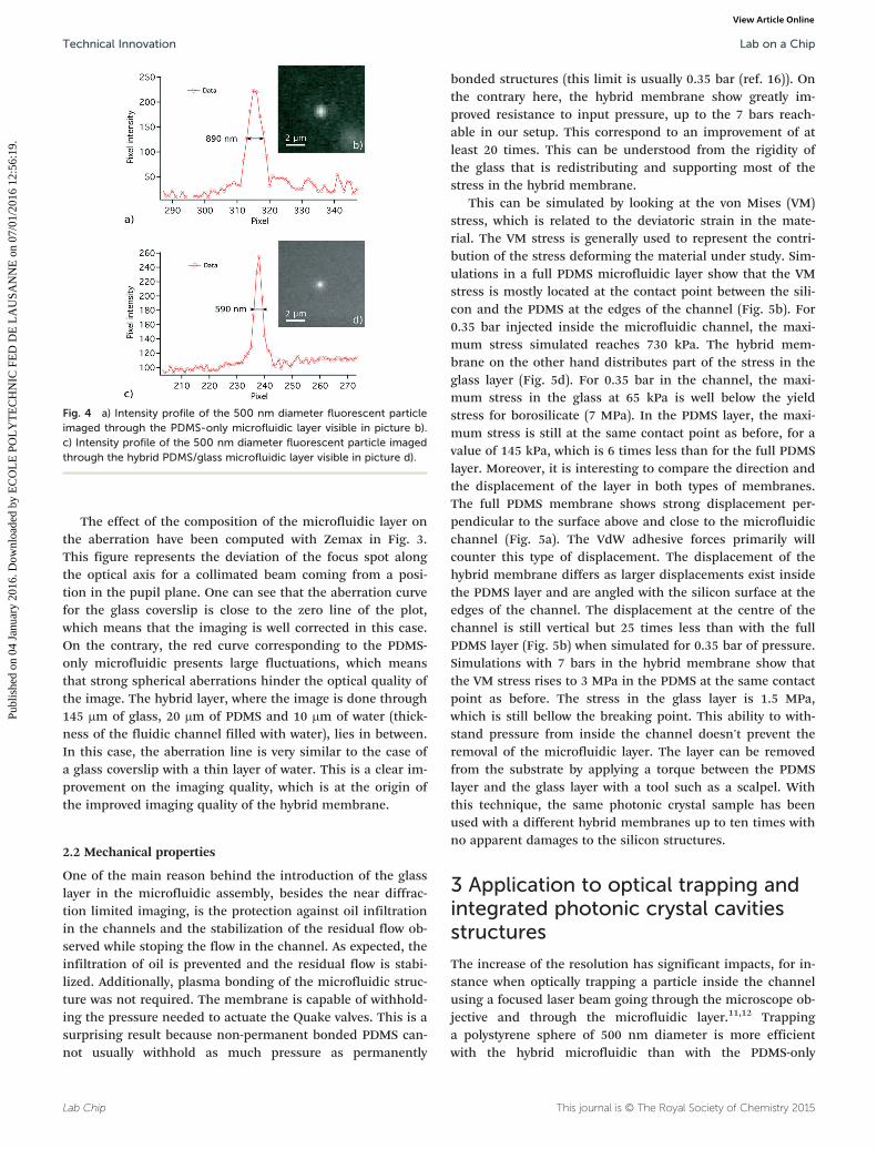
This improvement can also be observed in Fig. 4 showingan image of a fluorescent particle with a diameter of 500 nm.The top image is done through the 170 μm PDMS-only layerwhile the bottom image is done through the hybrid layer.The same immersion objective is used in both cases. The im-age of the particle obtained through the PDMS-only micro-fluidics as a full width at half maximum (FWHM) of 890 nm.When imaging the same kind of particle with the hybridPDMS/glass microfluidic, the FWHM is reduced to 590 nm.These particles have a fluorescent emission around 600 nm.A Zemax simulation shows that the diffraction-limitedFWHM of such particles is 500 nm.
Fig. 2 Image of the final device with the microfluidic layer. a) Silicon sample with photonic crystal and waveguide in the red area. b) PDMS layerfor the fluid and nanoparticles. The fluidic microchannel is the channel with a U shape. c) Glass layer where the control channels are injected withpressurized air. d) PDMS interconnect block.
Fig. 3 Aberration calculated for several micfrofluidics layer. Inserts:Images from the adapted NBS1010A microscopy resolution targets.Cut-off frequency for the full PDMS layer is at 1400 lines per mmwhereas the cut-off is at 2200 lines per mm for thehybridmicrofluidics. Illumination wavelength is 520 nm.
Lab on a Chip Technical Innovation
Publ
ishe
d on
04
Janu
ary
2016
. Dow
nloa
ded
by E
CO
LE
PO
LY
TE
CH
NIC
FE
D D
E L
AU
SAN
NE
on
07/0
1/20
16 1
2:56
:19.
View Article Online
Lab Chip This journal is © The Royal Society of Chemistry 2015
The effect of the composition of the microfluidic layer onthe aberration have been computed with Zemax in Fig. 3.This figure represents the deviation of the focus spot alongthe optical axis for a collimated beam coming from a posi-tion in the pupil plane. One can see that the aberration curvefor the glass coverslip is close to the zero line of the plot,which means that the imaging is well corrected in this case.On the contrary, the red curve corresponding to the PDMS-only microfluidic presents large fluctuations, which meansthat strong spherical aberrations hinder the optical quality ofthe image. The hybrid layer, where the image is done through145 μm of glass, 20 μm of PDMS and 10 μm of water (thick-ness of the fluidic channel filled with water), lies in between.In this case, the aberration line is very similar to the case ofa glass coverslip with a thin layer of water. This is a clear im-provement on the imaging quality, which is at the origin ofthe improved imaging quality of the hybrid membrane.
2.2 Mechanical properties
One of the main reason behind the introduction of the glasslayer in the microfluidic assembly, besides the near diffrac-tion limited imaging, is the protection against oil infiltrationin the channels and the stabilization of the residual flow ob-served while stoping the flow in the channel. As expected, theinfiltration of oil is prevented and the residual flow is stabi-lized. Additionally, plasma bonding of the microfluidic struc-ture was not required. The membrane is capable of withhold-ing the pressure needed to actuate the Quake valves. This is asurprising result because non-permanent bonded PDMS can-not usually withhold as much pressure as permanently
bonded structures (this limit is usually 0.35 bar (ref. 16)). Onthe contrary here, the hybrid membrane show greatly im-proved resistance to input pressure, up to the 7 bars reach-able in our setup. This correspond to an improvement of atleast 20 times. This can be understood from the rigidity ofthe glass that is redistributing and supporting most of thestress in the hybrid membrane.
This can be simulated by looking at the von Mises (VM)stress, which is related to the deviatoric strain in the mate-rial. The VM stress is generally used to represent the contri-bution of the stress deforming the material under study. Sim-ulations in a full PDMS microfluidic layer show that the VMstress is mostly located at the contact point between the sili-con and the PDMS at the edges of the channel (Fig. 5b). For0.35 bar injected inside the microfluidic channel, the maxi-mum stress simulated reaches 730 kPa. The hybrid mem-brane on the other hand distributes part of the stress in theglass layer (Fig. 5d). For 0.35 bar in the channel, the maxi-mum stress in the glass at 65 kPa is well below the yieldstress for borosilicate (7 MPa). In the PDMS layer, the maxi-mum stress is still at the same contact point as before, for avalue of 145 kPa, which is 6 times less than for the full PDMSlayer. Moreover, it is interesting to compare the direction andthe displacement of the layer in both types of membranes.The full PDMS membrane shows strong displacement per-pendicular to the surface above and close to the microfluidicchannel (Fig. 5a). The VdW adhesive forces primarily willcounter this type of displacement. The displacement of thehybrid membrane differs as larger displacements exist insidethe PDMS layer and are angled with the silicon surface at theedges of the channel. The displacement at the centre of thechannel is still vertical but 25 times less than with the fullPDMS layer (Fig. 5b) when simulated for 0.35 bar of pressure.Simulations with 7 bars in the hybrid membrane show thatthe VM stress rises to 3 MPa in the PDMS at the same contactpoint as before. The stress in the glass layer is 1.5 MPa,which is still bellow the breaking point. This ability to with-stand pressure from inside the channel doesn't prevent theremoval of the microfluidic layer. The layer can be removedfrom the substrate by applying a torque between the PDMSlayer and the glass layer with a tool such as a scalpel. Withthis technique, the same photonic crystal sample has beenused with a different hybrid membranes up to ten times withno apparent damages to the silicon structures.
3 Application to optical trapping andintegrated photonic crystal cavitiesstructures
The increase of the resolution has significant impacts, for in-stance when optically trapping a particle inside the channelusing a focused laser beam going through the microscope ob-jective and through the microfluidic layer.11,12 Trappinga polystyrene sphere of 500 nm diameter is more efficientwith the hybrid microfluidic than with the PDMS-only
Fig. 4 a) Intensity profile of the 500 nm diameter fluorescent particleimaged through the PDMS-only microfluidic layer visible in picture b).c) Intensity profile of the 500 nm diameter fluorescent particle imagedthrough the hybrid PDMS/glass microfluidic layer visible in picture d).
Lab on a ChipTechnical Innovation
Publ
ishe
d on
04
Janu
ary
2016
. Dow
nloa
ded
by E
CO
LE
PO
LY
TE
CH
NIC
FE
D D
E L
AU
SAN
NE
on
07/0
1/20
16 1
2:56
:19.
View Article Online

Lab ChipThis journal is © The Royal Society of Chemistry 2015
microfluidic. This is demonstrated when plotting the cen-troid of the position of the center of emission of a nanoparti-cle of 500 nm in polystyrene trapped with the same amount
of power in both case in Fig. 6. From this data it is possibleto measure the trap stiffness k of the optical tweezer in bothcases, using the equipartition theorem: k = kBT/σ
2 where σ isthe standard deviation. We find that the trap stiffness of theoptical tweezer through the hybrid layer is almost 20 timeslarger than with the PDMS-only microfluidic. This in turns al-lows trapping spheres that are smaller in size with the samepower.
As an illustration it was used to bring particles close tophotonic nanostructures for integrated optical trapping usinghollow photonic crystal cavities.11,12 The results in these pa-pers were obtained using a thin PDMS-only microfluidicmembrane. The control of the flow inside the microfluidicchannel is important for this application, since the measure-ments have to be in a stable environment. For the experi-ments, the flow was completely stopped so that the particlescan be in Brownian motion with no external drift. The otherfunction of the layer is to provide good optical qualities in or-der to record the motion of the trapped nanoparticles usinginterferometry.17 For this method, a laser beam is focused onthe particle with an oil immersion objective. These measure-ments have the best lateral resolution when the focus spot ofthe detection laser is as small as possible.18 Moreover, classi-cal optical trapping of nanoparticles can be performed with abeam passing through the membrane in order to positionthem in the photonic crystal cavities, as demonstrated in thevideo in the additional material. More complex microfluidicchannels can be realized inside the PDMS layer, with the cor-responding valves, or other fluidic channels in the glass.
Fig. 5 a) FEM simulation of the displacement of the PDMS layer under a pressure of 0.35 bar inside the fluidic channel. The arrow length isnormalized and only indicates the direction of the displacement. The surface between the PDMS and the silicon is fixed. b) FEM simulation of thevon Mises stress inside the PDMS layer (quadratic scaling). c) FEM simulation of the displacement of the hybrid PDMS and glass layer withnormalized arrows under 0.35 bar of pressure. The magnitude of the displacement is more than 10 times less than with the full PDMSmicrofluidics for the same applied pressure. d) FEM simulation of the von Mises stress inside the PDMS and glass layers (non linear scaling). Themagnitude of the stress is 6 times less than with the full PDMS microfluidics.
Fig. 6 a) Histogram of the centroid of the position of trapped 500 nmpolystyrene particles within the PDMS-only microfluidic layer. b) Histo-gram of the centroid of the position of trapped 500 nm polystyreneparticles within the hybrid PDMS/glass microfluidic. The laser used totrap the particules in a) and b) is a Ti:Sapph operating at 900 nm, withthe same output power of 100 mW in both cases.
Lab on a Chip Technical Innovation
Publ
ishe
d on
04
Janu
ary
2016
. Dow
nloa
ded
by E
CO
LE
PO
LY
TE
CH
NIC
FE
D D
E L
AU
SAN
NE
on
07/0
1/20
16 1
2:56
:19.
View Article Online
Lab Chip This journal is © The Royal Society of Chemistry 2015
4 Conclusion
We present a microfluidic membrane that can be laid on topof opaque samples. Because of its composition, it can beused to make high resolution images of structures embeddedin the microfluidic channel through the membrane. Thanksto this hybrid microfluidic structure, the resolution of ourexperiments is increased, which enable us to track theBrownian motion more efficiently. Moreover, optical trappingperformed by an external laser through the microfluidicsgives a trap with a stiffness 20 times larger in our hybriddesign compared to the design with PDMS layers only.Finally, we also show the ability to integrate Quake valves inthis design in order to control the flow in the fluidic channeland is very resistant to injected pressure up to 7 bar withoutpermanent bonding to the sample required.
Acknowledgements
The authors acknowledge the financial support from the SwissNational Science Foundation Project No. 200020_153538. Theauthors thank H. P. Herzig and T. Scharf for the Zemax simu-lations, and M. Sabry for helpful discussions.
References
1 J. C. Mcdonald, D. C. Duffy, J. R. Anderson and D. T. Chiu,Electrophoresis, 2000, 21, 27–40.
2 H. Becker and L. E. Locascio, Talanta, 2002, 56, 267–287.3 G. M. Whitesides, Nature, 2006, 442, 368–373.
4 E. Berthier, E. W. K. Young and D. Beebe, Lab Chip,2012, 12, 1224.
5 T. Squires, Rev. Mod. Phys., 2005, 77, 977–1026.6 J. E. Baker, R. Sriram and B. L. Miller, Lab Chip, 2015, 15,
971–990.7 Z. Wang, H. Yan, S. Chakravarty, H. Subbaraman, X. Xu, D.
Fan, A. X. Wang and R. T. Chen, Opt. Lett., 2015, 40, 1563–1566.8 M. G. Scullion, Y. Arita, T. F. Krauss and K. Dholakia,
Optica, 2015, 2, 816–821.9 O. Krupin, C. Wang and P. Berini, Lab Chip, 2015, 15,
4156–4165.10 R. Mukhopadhyay, Anal. Chem., 2007, 3249–3253.11 M. Scullion, A. D. Falco and T. Krauss, Biosens. Bioelectron.,
2011, 27, 101–105.12 N. Descharmes, U. P. Dharanipathy, Z. Diao, M. Tonin and
R. Houdré, Lab Chip, 2013, 13, 3268–3274.13 N. Descharmes, U. P. Dharanipathy, Z. Diao, M. Tonin and
R. Houdré, Phys. Rev. Lett., 2013, 110, 123601.14 J. Ng Lee, C. Park and G. M. Whitesides, Anal. Chem.,
2003, 75, 6544–6554.15 M. A. Unger, H.-P. Chou, T. Thorsen, A. Scherer and S. R.
Quake, Science, 2000, 288, 113–116.16 J. C. Mcdonald, M. L. Chabinyc, S. J. Metallo, J. R. Anderson,
A. D. Stroock and G. M. Whitesides, Anal. Chem., 2002, 74,1537–1545.
17 A. Pralle, M. Prummer, E.-L. Florin, E. Stelzer and J. Hörber,Microsc. Res. Tech., 1999, 44, 378–386.
18 A. Rohrbach and E. H. K. Stelzer, J. Appl. Phys., 2002, 91,5474–5488.
Lab on a ChipTechnical Innovation
Publ
ishe
d on
04
Janu
ary
2016
. Dow
nloa
ded
by E
CO
LE
PO
LY
TE
CH
NIC
FE
D D
E L
AU
SAN
NE
on
07/0
1/20
16 1
2:56
:19.
View Article Online