Embed Size (px)
Citation preview
Lab on a Chip
Supplement
Lab Chip, 2014 | 1
Nanoshuttles propelled by motor proteins sequentially assemble molecular cargo in a microfluidic device
Electronic Supplementary InformationDirk Steuerwald, Susanna M. Früh, Rudolf Griss, Robert D. Lovchik and Viola Vogel
The Electronic Supplementary Information contains 3 videos (separate files), 7 supplemental figures and how we estimated the wall shear stresses.
(video 1): 3D animated z-stack of the channel geometry obtained from 44 confocal laser scanning microscopy (CLSM) images. The two loading streams of neutravidin (NA) as first cargo (green) and of DNA-cargo (blue) are clearly visible, separated by sharp hydrodynamic boarders. Silicon surfaces of the device show up in light blue. The image of the xz-projection is shown in Figure 1B
(video 2): Kinesin-propelled nanoshuttles sequentially load up cargo. Nanoshuttles (red) pass first through the NA-cargo loading stream (green) and then the DNA-cargo loading stream (blue) and capture the respective cargo as visualized by a time lapse sequence of confocal laser scanning microscopy (CLSM) images (40 times accelerated video, 4 frames per second). Silicon surface appears in light blue. Channel geometry as depicted in Fig. 2B.
(video 3): Nanoshuttle movement in an earlier generation channel design with the outlet vias directly above the intersections as depicted in Figure S4. Time lapse of confocal laser scanning microscopy (CLSM) images shows how the nanoshuttles (red) pass through the NA- (green) as well as the DNA-cargo loading stream (blue) and sequentially capture cargo. Silicon surface of the device appears in green. 40 times accelerated movie (4 frames per second).
Seven figures are provided below, showing (S1) images of the utilized chip, (S2) the dimensions of the design in a to-scale sketch, (S3) a comparison between the intended and the actual flow profile in the channel presented in the main paper, (S4) an earlier generation channel design with the outlets right above the intersections, which resulted in leaky stream boundaries, (S5) a design in which in-and outlets were in the same plane and loss rate of nanoshuttles was very high, (S6) a design similar to the one shown in S5 but with PTFE nanotracks and (S7) with a histogram showing the efficiency of the designs shown in S5 and S6. An example for the shear stress calculation is attached.
Electronic Supplementary Material (ESI) for Lab on a Chip.This journal is © The Royal Society of Chemistry 2014
Lab on a Chip
Supplement
Lab Chip, 2014 | 2
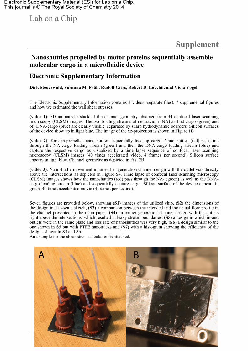
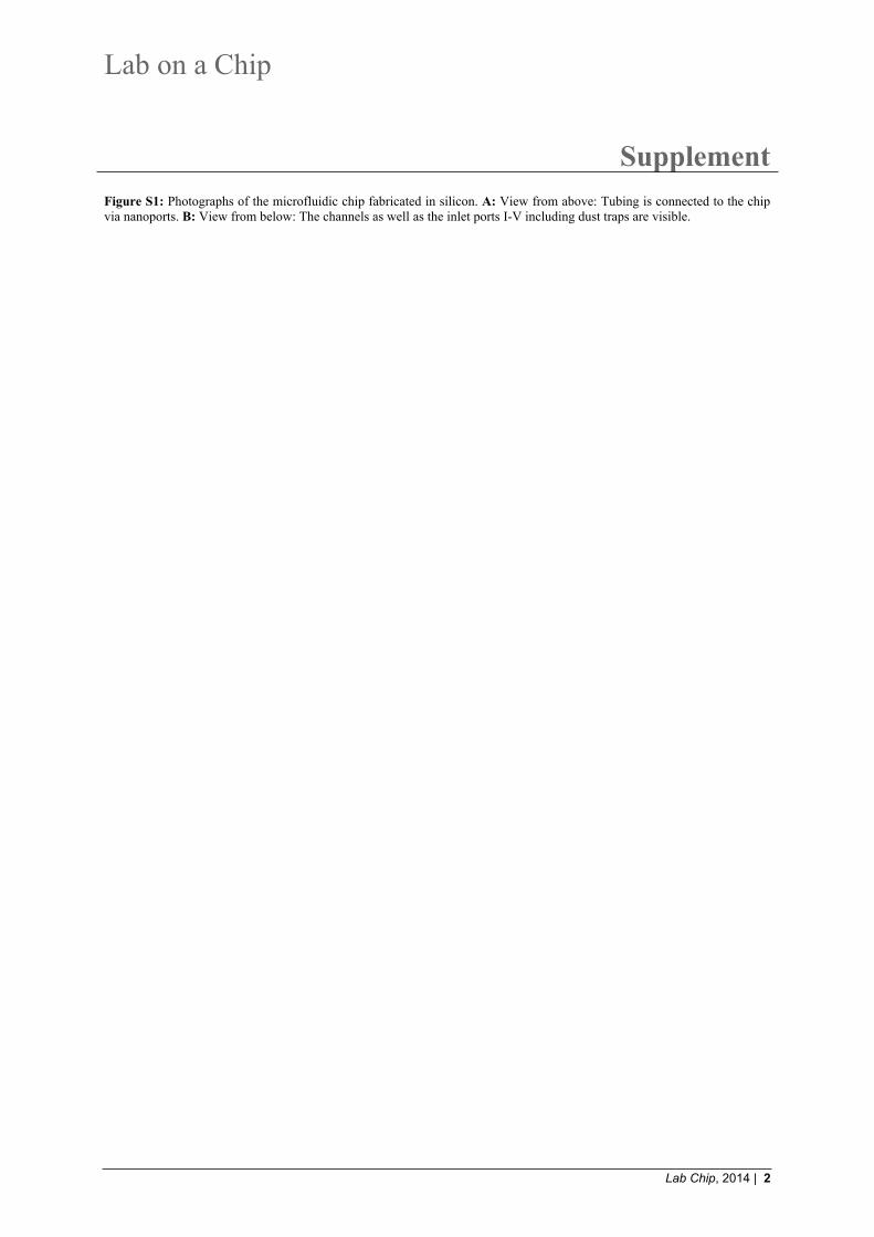
Figure S1: Photographs of the microfluidic chip fabricated in silicon. A: View from above: Tubing is connected to the chip via nanoports. B: View from below: The channels as well as the inlet ports I-V including dust traps are visible.
Lab Chip, 2014 | 3
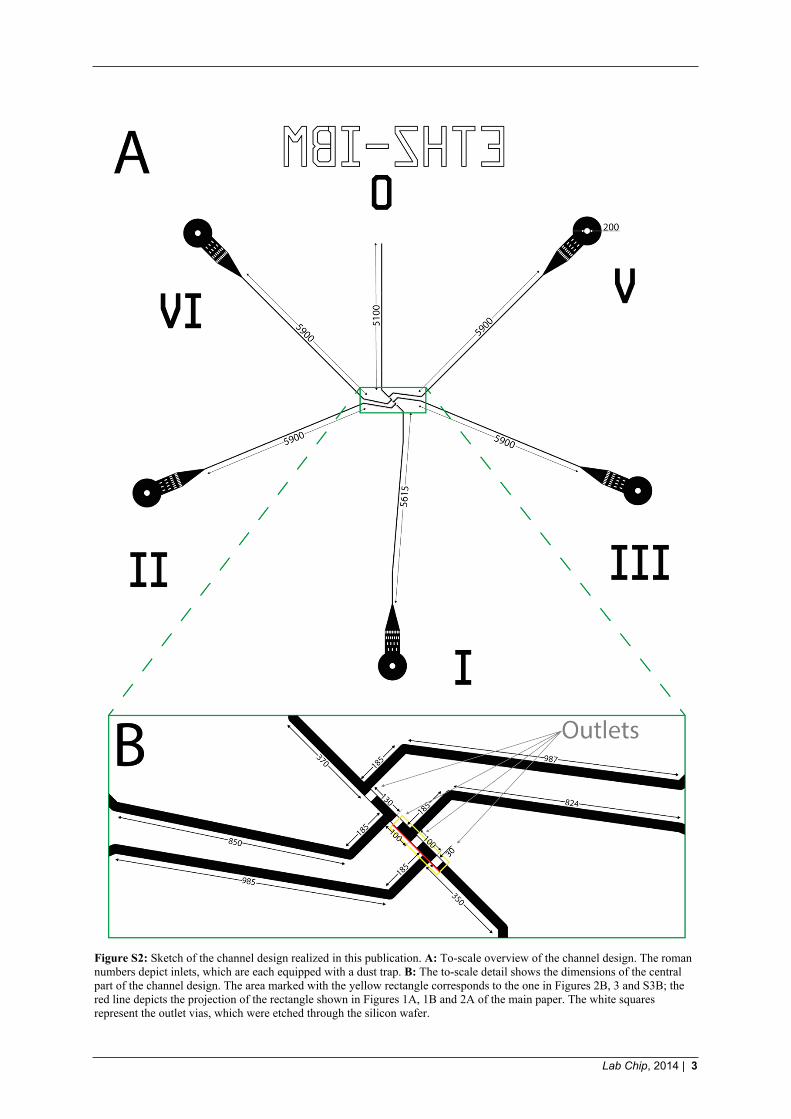
Figure S2: Sketch of the channel design realized in this publication. A: To-scale overview of the channel design. The roman numbers depict inlets, which are each equipped with a dust trap. B: The to-scale detail shows the dimensions of the central part of the channel design. The area marked with the yellow rectangle corresponds to the one in Figures 2B, 3 and S3B; the red line depicts the projection of the rectangle shown in Figures 1A, 1B and 2A of the main paper. The white squares represent the outlet vias, which were etched through the silicon wafer.
Lab Chip, 2014 | 4
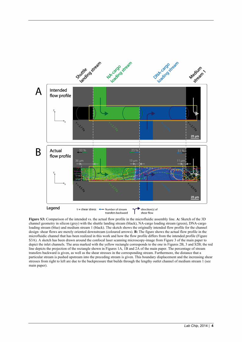
Figure S3: Comparison of the intended vs. the actual flow profile in the microfluidic assembly line. A: Sketch of the 3D channel geometry in silicon (grey) with the shuttle landing stream (black), NA-cargo loading stream (green), DNA-cargo loading stream (blue) and medium stream 1 (black). The sketch shows the originally intended flow profile for the channel design: shear flows are merely oriented downstream (coloured arrows). B: The figure shows the actual flow profile in the microfluidic channel that has been realized in this work and how the flow profile differs from the intended profile (Figure S3A). A sketch has been drawn around the confocal laser scanning microscopy-image from Figure 3 of the main paper to depict the inlet channels. The area marked with the yellow rectangle corresponds to the one in Figures 2B, 3 and S2B; the red line depicts the projection of the rectangle shown in Figures 1A, 1B and 2A of the main paper. The percentage of stream transfers backward is given, as well as the shear stresses in the corresponding stream. Furthermore, the distance that a particular stream is pushed upstream into the preceding stream is given. This boundary displacement and the increasing shear stresses from right to left are due to the backpressure that builds through the lengthy outlet channel of medium stream 1 (see main paper).
Lab Chip, 2014 | 5
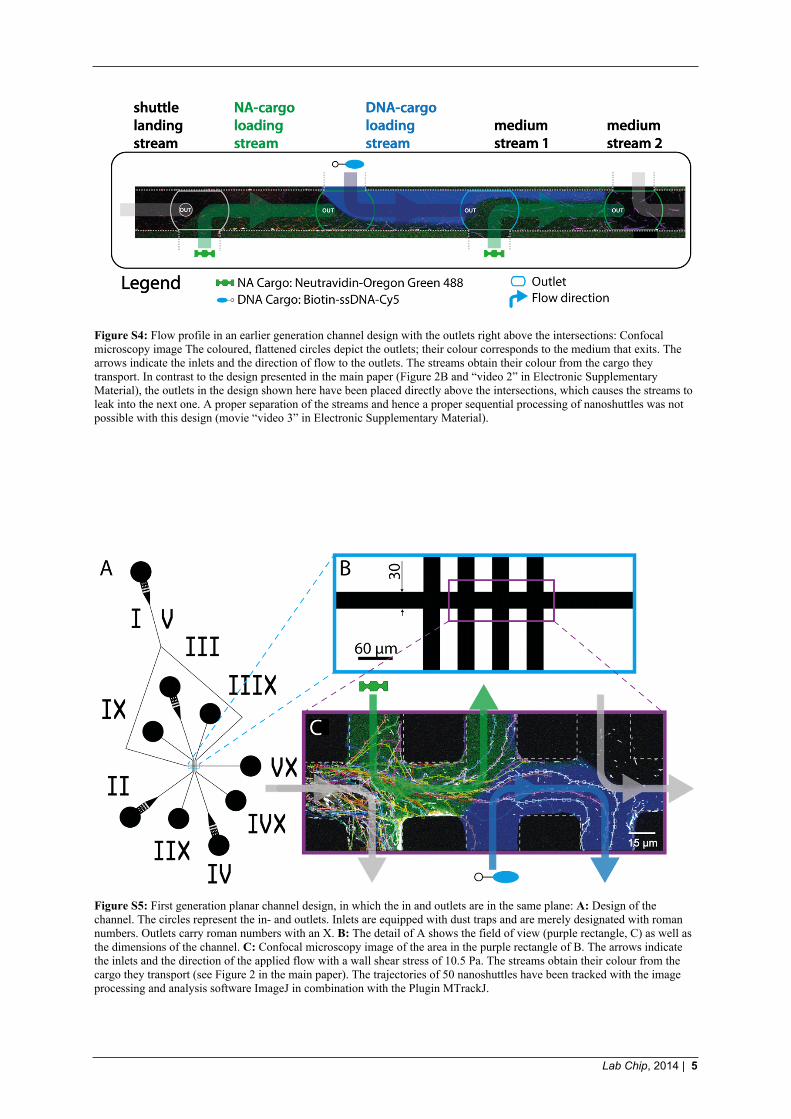
Figure S4: Flow profile in an earlier generation channel design with the outlets right above the intersections: Confocal microscopy image The coloured, flattened circles depict the outlets; their colour corresponds to the medium that exits. The arrows indicate the inlets and the direction of flow to the outlets. The streams obtain their colour from the cargo they transport. In contrast to the design presented in the main paper (Figure 2B and “video 2” in Electronic Supplementary Material), the outlets in the design shown here have been placed directly above the intersections, which causes the streams to leak into the next one. A proper separation of the streams and hence a proper sequential processing of nanoshuttles was not possible with this design (movie “video 3” in Electronic Supplementary Material).
Figure S5: First generation planar channel design, in which the in and outlets are in the same plane: A: Design of the channel. The circles represent the in- and outlets. Inlets are equipped with dust traps and are merely designated with roman numbers. Outlets carry roman numbers with an X. B: The detail of A shows the field of view (purple rectangle, C) as well as the dimensions of the channel. C: Confocal microscopy image of the area in the purple rectangle of B. The arrows indicate the inlets and the direction of the applied flow with a wall shear stress of 10.5 Pa. The streams obtain their colour from the cargo they transport (see Figure 2 in the main paper). The trajectories of 50 nanoshuttles have been tracked with the image processing and analysis software ImageJ in combination with the Plugin MTrackJ.
Lab Chip, 2014 | 6
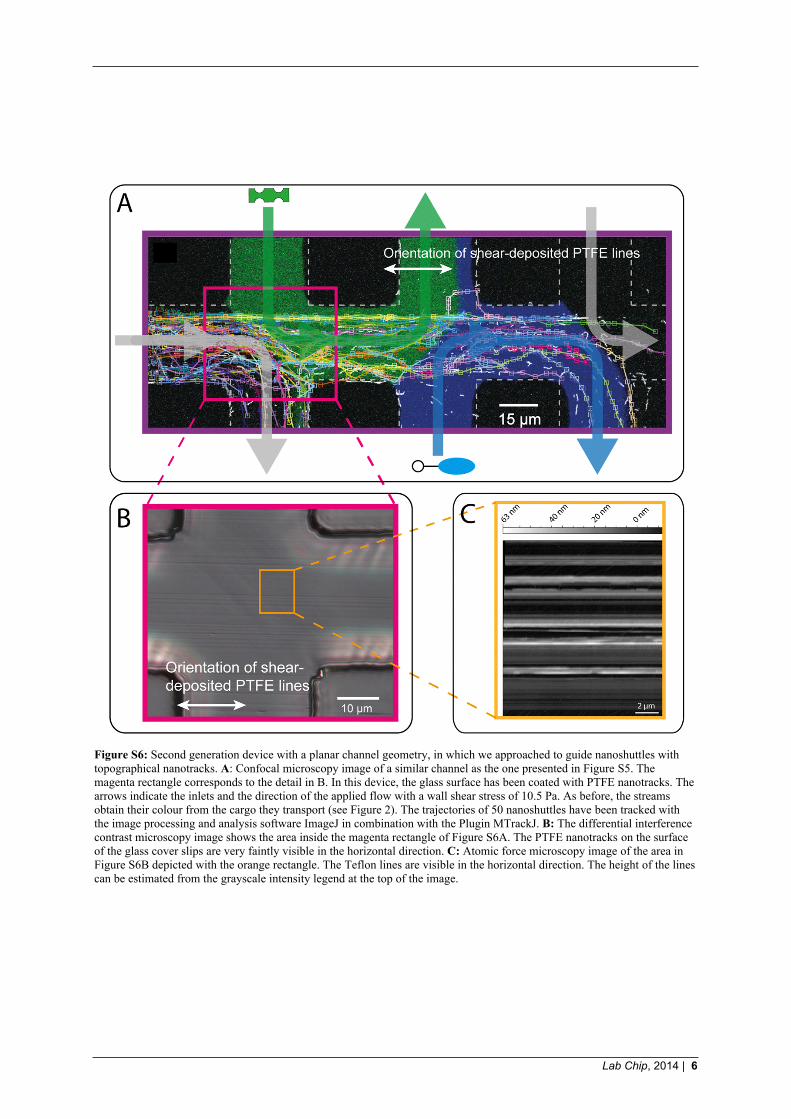
Figure S6: Second generation device with a planar channel geometry, in which we approached to guide nanoshuttles with topographical nanotracks. A: Confocal microscopy image of a similar channel as the one presented in Figure S5. The magenta rectangle corresponds to the detail in B. In this device, the glass surface has been coated with PTFE nanotracks. The arrows indicate the inlets and the direction of the applied flow with a wall shear stress of 10.5 Pa. As before, the streams obtain their colour from the cargo they transport (see Figure 2). The trajectories of 50 nanoshuttles have been tracked with the image processing and analysis software ImageJ in combination with the Plugin MTrackJ. B: The differential interference contrast microscopy image shows the area inside the magenta rectangle of Figure S6A. The PTFE nanotracks on the surface of the glass cover slips are very faintly visible in the horizontal direction. C: Atomic force microscopy image of the area in Figure S6B depicted with the orange rectangle. The Teflon lines are visible in the horizontal direction. The height of the lines can be estimated from the grayscale intensity legend at the top of the image.
Lab Chip, 2014 | 7
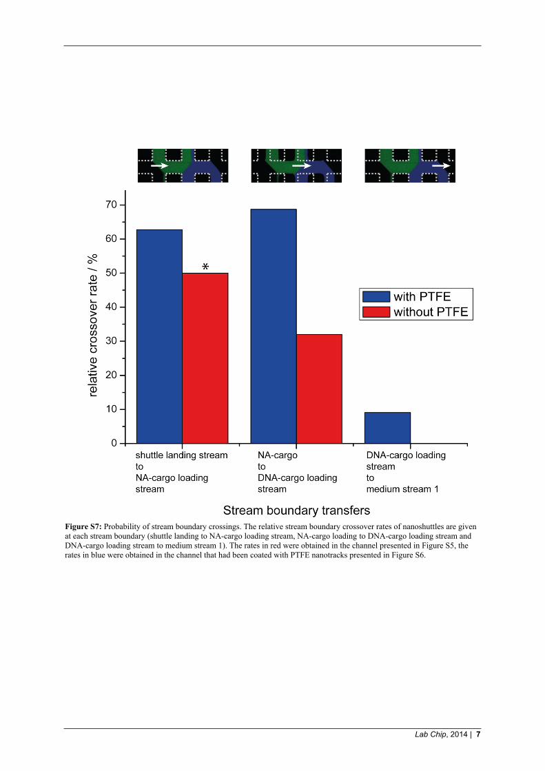
Figure S7: Probability of stream boundary crossings. The relative stream boundary crossover rates of nanoshuttles are given at each stream boundary (shuttle landing to NA-cargo loading stream, NA-cargo loading to DNA-cargo loading stream and DNA-cargo loading stream to medium stream 1). The rates in red were obtained in the channel presented in Figure S5, the rates in blue were obtained in the channel that had been coated with PTFE nanotracks presented in Figure S6.
Lab Chip, 2014 | 8
Wall shear stress calculation:
The wall shear stress in the demonstrated microfluidic device was calculated as follows. According to Kim et al, the average wall shear stress is expressed with the cross-sectional area, entire surface area and the pressure gradient1,2:
(equation 1)𝜏𝑊 = ∆𝑃𝑠𝑦𝑟 ∙
𝐴𝑥
𝐴𝑠
𝜏𝑊:𝑤𝑎𝑙𝑙 𝑠ℎ𝑒𝑎𝑟 𝑠𝑡𝑟𝑒𝑠𝑠[𝑁 ∙ 𝑚2]𝐴𝑥:𝑐𝑟𝑜𝑠𝑠 ‒ 𝑠𝑒𝑐𝑡𝑖𝑜𝑛𝑎𝑙 𝑎𝑟𝑒𝑎 𝑜𝑓 𝑡ℎ𝑒 𝑚𝑖𝑐𝑟𝑜𝑐ℎ𝑎𝑛𝑛𝑒𝑙; 𝐴𝑠:𝑒𝑛𝑡𝑖𝑟𝑒 𝑠𝑢𝑟𝑓𝑎𝑐𝑒 𝑎𝑟𝑒𝑎 𝑜𝑓 𝑡ℎ𝑒 𝑚𝑖𝑐𝑟𝑜𝑐ℎ𝑎𝑛𝑛𝑒𝑙;
∆𝑃𝑠𝑦𝑟:𝑔𝑎𝑢𝑔𝑒 𝑝𝑟𝑒𝑠𝑠𝑢𝑟𝑒 𝑏𝑒𝑡𝑤𝑒𝑒𝑛 𝑡ℎ𝑒 𝑒𝑛𝑑 𝑜𝑓 𝑡ℎ𝑒 𝑐𝑎𝑝𝑖𝑙𝑙𝑎𝑟𝑦 𝑎𝑛𝑑 𝑡ℎ𝑒 𝑜𝑝𝑝𝑜𝑠𝑖𝑡𝑒 𝑒𝑛𝑑 𝑜𝑓 𝑡ℎ𝑒 𝑚𝑖𝑐𝑟𝑜𝑐ℎ𝑎𝑛𝑛𝑒𝑙.
In which:
(equation 2)𝐴𝑥 = ℎ ∙ 𝑤and
(equation 3)𝐴𝑠 = 𝐿 ∙ 𝑤
ℎ:ℎ𝑒𝑖𝑔ℎ𝑡 𝑜𝑓 𝑡ℎ𝑒 𝑚𝑖𝑐𝑟𝑜𝑐ℎ𝑎𝑛𝑛𝑒𝑙 [𝑚];𝑤:𝑤𝑖𝑑𝑡ℎ 𝑜𝑓 𝑡ℎ𝑒 𝑚𝑖𝑐𝑟𝑜𝑐ℎ𝑎𝑛𝑛𝑒𝑙 [𝑚]; 𝐿:𝑙𝑒𝑛𝑡ℎ 𝑜𝑓 𝑡ℎ𝑒 𝑚𝑖𝑐𝑟𝑜𝑐ℎ𝑎𝑛𝑛𝑒𝑙
According to the Hagen-Poiseuille law, a constant pressure drop results in a constant flow rate Q3:
(equation 4)∆𝑃 = 𝑅ℎ𝑦𝑑 ∙ 𝑄
𝑅ℎ𝑦𝑑: ℎ𝑦𝑑𝑟𝑜𝑙𝑖𝑐 𝑟𝑒𝑠𝑖𝑠𝑡𝑎𝑛𝑐𝑒; 𝑄:𝑣𝑜𝑙𝑢𝑚𝑒𝑡𝑟𝑖𝑐 𝑓𝑙𝑜𝑤 𝑟𝑎𝑡𝑒 [𝑚3 ∙ 𝑠 ‒ 1]
The hydraulic resistance for straight channels with a rectangular cross-sectional area calculates to3:
(equation 5)
𝑅ℎ𝑦𝑑 =12 ∙ 𝜂 ∙ 𝐿
1 ‒ 0.63 ∙ (ℎ𝑤
)∙
1
ℎ3 ∙ 𝑤
𝜂:𝑑𝑦𝑛𝑎𝑚𝑖𝑐 𝑣𝑖𝑠𝑐𝑜𝑠𝑖𝑡𝑦 𝑜𝑓 𝑡ℎ𝑒 𝑓𝑙𝑢𝑖𝑑 [𝑁 ∙ 𝑚 ‒ 2 ∙ 𝑠];
Combining the equations 1-5 results in:
(equation 6)
𝜏𝑊 = 12 ∙ 𝜂
1 ‒ 0.63 ∙ (ℎ𝑤
)∙
1
ℎ2 ∙ 𝑤𝑄
Calculation of the shear stress for an aqueous solution (η: ) with a volumetric flow rate of 1.5 1 𝑚𝑃𝑎 ∙ 𝑠µL/min in a channel with a rectangular cross-sectional with a height of 40 µm and a width of 30 µm for (since in our case, h>w, the values for h and w have been exchanged in equation 7):
𝜏𝑊 =12 ∙ 1 ∙ 10 ‒ 3𝑁 𝑚 ‒ 2 𝑠
1 ‒ 0.63 ∙30 ∙ 10 ‒ 6𝑚
40 ∙ 10 ‒ 6𝑚
1
(30 ∙ 10 ‒ 6𝑚)2 ∙ 40 ∙ 10 ‒ 6𝑚 ∙ 2.5 ∙ 10 ‒ 11 ∙ 𝑚3 ∙ 𝑠 ‒ 1
(equation 7)

Lab Chip, 2014 | 9
The resulting wall shear stress in this device at a volumetric flow rate of 1.5 µL/min was calculated to be 15.80 Pa.
Lab Chip, 2014 | 10
References
1. T. Kim, M.-T. Kao, E. Meyhofer, and E. F. Hasselbrink, Nanotechnology, 2006, 18, 025101.2. F. M. White, Viscous Fluid Flow, McGraw-Hill, 2006.3. H. Bruus, Theoretical Microfluidics, Oxford University Press, 2008.