Embed Size (px)
Citation preview

Fachbereich 08 - Biologie und Chemie
Institut für Anorganische und Analytische Chemie
der Justus-Liebig-Universität Giessen
Label-free electrical biosensing based
on electrochemically functionalized
carbon nanostructures
DISSERTATION
to apply for the degree of „Doctor rerum naturalium“
(Dr. rer. nat.)
submitted by
Tetiana Kurkina
born March 01, 1984
in Brovary, Kyiv obl. (Ukraine)
Gießen, February 2012

REFEREES: 1. PROF. DR. BERNHARD SPENGLER 1
2. PROF. DR. JÜRGEN JANEK 2
3. PROF. DR. KLAUS KERN 3,4
THE FOLLOWING WORK WAS CARRIED OUT BETWEEN DECEMBER 2008 AND DECEMBER 2011
AT THE MAX PLANCK INSTITUTE FOR SOLID STATE RESEARCH, STUTTGART, GERMANY.
1 Institut für Anorganische und Analytische Chemie, Justus-Liebig-Universität Gießen 2 Physikalisch-Chemisches Institut, Justus-Liebig-Universität Gießen 3 Max-Planck-Institut für Festkörperforschung, Stuttgart 4 Institut de Physique de la Matière Condensée, Ecole Polytechnique Fédérale de Lausanne,
Switzerland

Abstract
The development of new analytical approaches in the diagnostics of the
diseases with higher throughput, smaller sample and set-up sizes, lower cost and
easier disposal is one of the major needs of modern medicine. Miniaturization and
simplification of biomedical assays are required for point of care diagnostics and lab-
on-a-chip systems. In this thesis the concept of electrical biosensors based on single
wall carbon nanotubes (SWCNTs) and graphene is presented. The detection of
saccharides and DNA was realized using field effect transistor (FET) - based sensors
where carbon nanostructures play the role of a transducing component.
The theoretical part of the thesis explains the concept of biosensing and
the role of nanomaterials in the development of the next generation of bioassays.
Furthermore, the structure and properties of SWCNTs and graphene and their
advantages for electrical biosensing are described.
The experimental section starts with a detailed description of the carbon
nanotube (CNT) biosensor fabrication process. This includes carbon nanotube
solution preparation, assembly of CNTs into devices, passivation of metal electrodes
and modification of the CNT surface with receptors. The advantages of using
impedance spectroscopy measurements at different liquid gate voltages for electrical
detection of biomolecules are pointed out here.
The next chapter is dedicated to affinity-based glucose sensing. Using
boronic acid functionalized carbon nanotubes the detection of glucose was
demonstrated. The sensing mechanism was investigated in detail. The sensor signal
was shown to be different depending on the way the CNTs were modified –
covalently or non-covalently.
The biosensing setup was then utilized for the detection of DNA. It was
possible to achieve very low limit of detection for oligonucleotides using CNTs non-
covalently modified with a complementary DNA sequence. The sensor was shown to
be highly selective as well.
Finally, the possibility of using 2D-carbon nanomaterial, namely
graphene, for electrical biosensing is outlined. The approaches towards large scale
preparation of graphene devices were investigated during this work. The wafer-scale

- 4 -
fabrication of reduced graphene oxide devices was realized using a novel chemical
route.
The final part of the thesis summarizes the results obtained while
conducting this work. The designed biosensing platforms based on carbon
nanostructures show a great promise for application in chemical analysis and
medical diagnostics. Therefore the developed biosensor is planned to be adapted for
the detection of analytes from biological liquids.
Keywords: biosensor, label-free detection, carbon nanotubes, graphene,
electrical detection

- 5 -
Zusammenfassung
Die Entwicklung neuer analytischer Ansätze mit höherem Durchsatz,
geringeren Probenmengen und kleineren Geräten, niedrigeren Kosten und
einfacherer Entsorgung ist eine der wichtigsten Bedürfnisse der modernen Medizin
für die Diagnostik von Erkrankungen. Die Miniaturisierung und die Vereinfachung
biomedizinischer Tests sind für die „Point of Care“ Diagnostik und für „Lab-on-a-
Chip“ Systeme erforderlich. In dieser Arbeit wird das Konzept elektrischer
Biosensoren basierend auf einwandigen Kohlenstoff-Nanoröhrchen (SWCNTs) und
Graphen präsentiert. Der Nachweis von Zuckern und DNS wurde in Form von
Feldeffekt-Transistor (FET) - Sensoren realisiert, wobei die elektronischen
Eigenschaften von Kohlenstoff Nanostrukturen durch an deren Oberfläche
stattfindenden chemische Reaktionen beeinflusst werden.
Der theoretische Teil der Arbeit erläutert das Konzept der Biosensorik,
insbesondere die Rolle von Nanomaterialien in der Entwicklung der nächsten
Generation von biologischen Assays. Des Weiteren sind die Struktur und die
Eigenschaften von SWCNTs und Graphen und deren Vorteile für die elektrische
Bioanalytik beschrieben.
Der experimentelle Teil beginnt mit einer ausführlichen Beschreibung der
Herstellung von SWCNT-Biosensoren. Dazu gehören die Dispergierung von
Kohlenstoff-Nanoröhrchen (CNT) in Lösung, die Integration von CNTs in
elektronische Bauteile, die Passivierung von Metallelektroden und die Modifizierung
der CNT Oberfläche mit Rezeptoren. Außerdem enthält diese Kapitel eine Erklärung
der Detektionsmethode und weist auf die Vorteile des gewählten Ansatzes für die
elektrische Detektion von Biomolekülen hin.
Das nächste Kapitel befasst sich mit der Affinität-basierten Detektion von
Zucker. Mittels Boronsäure-Rezeptoren wurde Glucose nachgewiesen. Der
Detektionsmechanismus wurde im Detail untersucht. Es konnte gezeigt werden, dass
sich je nach Modifizierungart (kovalente oder nicht-kovalente Bindung von
Rezeptore) das Sensorsignal unterschiedlich verhält.
Derselbe Biosensorik Aufbau wurde dann für den Nachweis von DNS
verwendet. Es war möglich, eine sehr niedrige Nachweisgrenze für Oligonukleotide
mit Hilfe von CNTs zu erreichen, die nicht-kovalent mit einer komplementären DNS-
Sequenz modifiziert waren. Zusätzlich war der Sensor selektiv für die Zielsubstanz.

- 6 -
Des Weiteren wurde der Einsatz von 2D-Kohlenstoff-Nanomaterial,
nämlich Graphen, für die elektrische Biosensorik erforscht. In diesem Kapitel werden
Ansätze zur großtechnischen Herstellung von Graphen Bauteilen beschrieben. Die
„Wafer-Scale“-Fertigung von reduzierten Graphenoxid Bauteilen unter Verwendung
einer neuartigen chemischen Methode wurde realisiert.
Der letzte Teil fasst die Ergebnisse dieser Arbeit zusammen. Die
entworfenen Biosensorik Konzepte basierend auf Kohlenstoff-Nanostrukturen sind
vielversprechend für die Anwendung in der chemischen Analytik und der
medizinischen Diagnostik. Daher ist es geplant, den entwickelten Biosensor für den
Nachweis von Analyten aus biologischen Flüssigkeiten anzupassen.
Schlagwörter: Biosensor, Marker-freie Erkennung, Kohlenstoff-
Nanoröhrchen, Graphen, elektrische Detektion

- 7 -
List of used acronyms
1D - one dimensional 2D - two dimensional
ABA - aminobenzoic acid AFM - atomic force microscopy
APBA - aminophenylboronic acid BA - boronic acid CE - counter electrode
CNT - carbon nanotube CVD - chemical vapor deposition DEP - dielectrophoresis
DMF - dimethylformamide DWCNT - double wall carbon nanotube
ECM - electrochemical modification EDC - ethylenediaminechloride FET - field-effect transistor
GO - graphene oxide GOx - glucose oxidase
ISFET - ion-selective field-effect transistor LoC - lab on a chip
µTAS - micro total analytical system MWCNT - multi wall carbon nanotube
ncDNA - non-complementary DNA NHS - N-hydroxysuccinimide
PDMS - polydimethylsiloxane PoC - point of care pTy RB
- -
polytyramine Rhodamin B
RE - reference electrode RGO - reduced graphene oxide
RT-PCR - real-time polymerase chain reaction SDBS - sodium dodecyl benzene sulfonate
SDS - sodium dodecyl sulfate SWCNT - single wall carbon nanotube
WE - working electrode

- 8 -
List of figures Figure 1.1. Schematic of a back-gated (a) and a liquid gated FET. ................................................................... - 17 -
Figure 1.2. Representation of the phase of impedance .................................................................................... - 18 -
Figure 2.1. Physical structure of CNTs. .............................................................................................................. - 20 -
Figure 2.2. The structure of double walled carbon nanotube (DWCNT) and multi-walled carbon nanotube
(MWCNT) .......................................................................................................................................................... - 21 -
Figure 2.3. Overview of different CNT-based biosensing strategies. ................................................................. - 22 -
Figure 2.4. The structure of graphene. .............................................................................................................. - 23 -
Figure 2.5. Non-covalent functionalization of carbon nanostructures with pyrene-derivatives via π-π stacking. 1-
pyrenebutanoic acid succinimidyl ester (PBASE) attached to a) graphene and b) CNT. .................................... - 25 -
Figure 2.6. Various covalent functionalization schemes for graphene oxide. ................................................... - 26 -
Figure 2.7. Addition reactions for the functionalization of the carbon nanotube sidewall ............................... - 27 -
Figure 2.8. Schemes for (a) oxidative ECM with 4-aminobenzylamine and (b) reductive ECM with an aryl
diazonium salt. .................................................................................................................................................. - 28 -
Figure 3.1. Visualization of the same SWCNT device with AFM and confocal microscopy. .............................. - 31 -
Figure 3.2. Schematic of the dielectrophoretic manipulation of 1D-nanostructures. ........................................ - 32 -
Figure 3.3. Schematic of the dielectrophoretic trapping setup ......................................................................... - 33 -
Figure 3.4. Different electrode geometries used in this study. .......................................................................... - 34 -
Figure 3.5. One of the possible ways to upscale the DEP trapping of CNTs. ..................................................... - 35 -
Figure 3.6. Monitoring the dielectrophoretic trapping of the nanotubes.......................................................... - 36 -
Figure 3.7. Passivation of Pt electrodes on Si/SiO2 surface.. ............................................................................. - 38 -
Figure 3.8. Scheme showing the functionalization strategy to obtain the BA-CNT-sensors. ............................. - 40 -
Figure 3.9. Gate dependence of the devices during (a) covalent and (b) non-covalent electrochemical
functionalization of CNTs with APBA. .............................................................................................................. - 41 -
Figure 3.10. Electrochemical functionalization of CNTs. ................................................................................... - 42 -
Figure 3.11. Detection strategy ......................................................................................................................... - 43 -
Figure 4.1. Sensing in the open system without applying liquid gate voltage. ................................................. - 46 -
Figure 4.2. (a) An AFM image of the electrode region of a BA-CNT sensor after the sensing trials. (b) A schematic
representation of the microfluidic set up with the location of the nanotube device. (c) a photograph of the final
assembled device. .............................................................................................................................................. - 47 -
Figure 4.3. Affinity sensing of saccharides......................................................................................................... - 48 -
Figure 4.4. 2D-impedance (Z-) maps showing the impedance as a function of frequency and liquid gate voltage.
Magnitude [Ohms] maps of the impedance of covalently functionalized BA-CNT devices are shown in buffer (a)
and in 10 mM glucose (b).. ................................................................................................................................ - 49 -
Figure 4.5. Reversibility of the binding of glucose in covalent-BA-CNT-sensors. ............................................... - 50 -
Figure 4.6. Concentration dependence of the covalent-BA-CNT-sensors .......................................................... - 51 -
Figure 4.7. Control experiment with unmodified CNT devices. .......................................................................... - 52 -
Figure 4.8. Selectivity of the covalent BA-CNT-sensors...................................................................................... - 53 -
Figure 4.9. Charge distribution on the surface of BA-functionalized CNTs calculated using the Henderson-
Hasselbach relationship. .................................................................................................................................... - 54 -
Figure 4.10. Sensor response for non-covalent-BA-CNT devices showing the gate dependence of the magnitude
of impedance at low frequencies ....................................................................................................................... - 56 -
Figure 5.1. Overview of the assembled carbon nanotube DNA sensor.. ............................................................ - 59 -
Figure 5.2. The controlled functionalization of the carbon nanotube surface with probe DNA. ....................... - 61 -
Figure 5.3. Evidence for the coupling of probe DNA: schematic of the experiment (a), AFM images taken before
(b) and after (c) the coupling protocol. .............................................................................................................. - 62 -
- 9 -
Figure 5.4. Evidence for DNA hybridization during the sensing trial ................................................................. - 64 -
Figure 5.5. Specificity of CNT-DNA-sensors ....................................................................................................... - 65 -
Figure 5.6. Control experiment with non-functionalized CNTs. ......................................................................... - 66 -
Figure 5.7. Attomolar detection limit of CNT-DNA-sensors. .............................................................................. - 67 -
Figure 5.8. Sensitivity of CNT-DNA-sensors. ...................................................................................................... - 68 -
Figure 5.9. Attomolar target differentiation in a heterogeneous DNA mixture. .............................................. - 69 -
Figure 6.1. Liquid phase exfoliation of graphene from graphite. ...................................................................... - 72 -
Figure 6.2. Preparation of graphene oxide solution .......................................................................................... - 73 -
Figure 6.3. An RGO device with passivated contacts for biosensing applications. ............................................ - 74 -
Figure 6.4. Liquid gating of RGO device. ............................................................................................................ - 75 -
Figure 6.5. Scheme of the chemical anchoring protocol. ................................................................................... - 76 -
Figure 6.6. Surface characterization by AFM. .................................................................................................... - 77 -
Figure 6.7. Electronic properties of the anchored GO devices ........................................................................... - 78 -
Figure 6.8. Scaling up the chemical anchoring.. ................................................................................................ - 80 -
Figure 6.9. Wafer scale RGO devices with high yield. ........................................................................................ - 81 -
Figure 6.10. AFM image (phase mode) of graphene oxide coupled to electrochemically modified electrodes on
flexible kapton substrate. .................................................................................................................................. - 82 -
Figure 6.11. Commercially available graphene oxide coupled to the electrodes. ............................................. - 82 -
Figure 7.1. Sensing of let-7a-miRNA in buffer (a) and serum (b). ...................................................................... - 85 -
Figure 7.2. AFM images of the device before (a) and after (b) sensing trials in serum. .................................... - 86 -
Figure 7.3. Schematic of RGO-FET- immunosensor. .......................................................................................... - 86 -
Figure 7.4. Sensing of beta-amyloid peptide using RGO immunosensor ........................................................... - 87 -

Table of Contents
Theoretical background ................................... - 12 -
1. Biosensors in medical diagnostics ..................... - 12 -
1.1. Introduction. .................................................................................................................... - 12 -
1.2. Operating principle and types of biosensors. ........................................................... - 13 -
1.3. Nanomaterials for the detection of biomolecules. ................................................... - 14 -
1.4. Electrical/electrochemical sensing. ............................................................................. - 15 -
2. Carbon nanostructures for biosensing ................ - 19 -
2.1. Introduction. .................................................................................................................... - 19 -
2.2. Carbon nanotubes. ......................................................................................................... - 19 -
2.3. Graphene. ......................................................................................................................... - 23 -
2.4. Functionalization of carbon nanostructures.............................................................. - 24 -
Experimental section ....................................... - 29 -
3. Fabrication of CNT-based sensors ..................... - 29 -
3.1. Introduction. .................................................................................................................... - 29 -
3.2. Preparation of CNT dispersions. ................................................................................. - 29 -
3.3. Visualization of CNT devices. ..................................................................................... - 30 -
3.4. Dielectrophoretic manipulation of CNTs. ................................................................. - 32 -
3.5. Passivation of electrodes. .............................................................................................. - 37 -
3.6. Chemical functionalization of CNTs. ......................................................................... - 39 -
3.7. Sensing strategy. ............................................................................................................. - 42 -
4. Sensing of saccharides .................................. - 45 -
4.1. Introduction. .................................................................................................................... - 45 -
4.2. Device fabrication. ......................................................................................................... - 46 -
4.3. Sensing results. ............................................................................................................... - 48 -
4.4. Conclusions. .................................................................................................................... - 57 -
5. Label-free detection of few copies of DNA.......... - 58 -

- 11 -
5.1. Introduction. .................................................................................................................... - 58 -
5.2. Sensing setup. ................................................................................................................. - 59 -
5.3. Functionalization of CNTs with probe DNA............................................................ - 60 -
5.4. Sensing trials. .................................................................................................................. - 63 -
5.5. Sensing results. ............................................................................................................... - 64 -
5.6. Sensitivity and detection limit. .................................................................................... - 67 -
5.7. Detection in complex media. ........................................................................................ - 69 -
5.8. Conclusions. .................................................................................................................... - 70 -
6. Towards graphene-based electrical sensors - 71 -
6.1. Introduction. .................................................................................................................... - 71 -
6.2. DEP trapping of graphene. ........................................................................................... - 72 -
6.3. DEP trapping of graphene oxide. ................................................................................ - 72 -
6.4. Chemical anchoring of graphene oxide for preparation of the devices. .............. - 75 -
6.5. Up-scaling the fabrication of RGO devices. .............................................................. - 79 -
6.6. Conclusions. .................................................................................................................... - 82 -
Summary and outlook ...................................... - 84 -
7.1. CNT based electrical sensors. ...................................................................................... - 84 -
7.2. Graphene devices for biosensing. ............................................................................... - 86 -
Bibliography .................................................. - 89 -
Acknowledgements ........................................ - 103 -

Theoretical background
1. Biosensors in medical diagnostics
1.1. Introduction. Early and correct diagnosis plays a very
important role in modern medicine. Medical diagnostics evolved far beyond the
evaluation of external symptoms. Doctors rely on the results of bio-/chemical tests
some of which were unknown thirty years ago. For decades researchers have been
working on the discovery of biomarkers – molecular indicators of different biological
states of the organism. As a result, the number of biomarkers for various diseases at
the different stages of pathology increased dramatically. Because of this in many
cases the disease can be counteracted before the appearance of the symptoms [1].
This has a huge impact on the economic and the social life. Increasing number of
biomarkers as well as the demand for fast and reliable medical tests are driving the
development of new analytical approaches that can be used in clinical biochemistry.
Medical diagnostics is enriched by advances in biochemistry, molecular biology,
physiology, chemistry and physics (optics, mechanics, electronics) [2]. Integrated
knowledge from different scientific fields is required to satisfy the need of modern
society for low-cost, fast, and reliable methods for the detection of different
biomarkers, the number of which is constantly growing [3]. The concept of Point of
care (PoC) diagnostics adds miniaturization, simplification and disposability to the
above mentioned desirable characteristics of new analytical techniques in medicine
[4, 5]. One of the approaches that would fit perfectly for this purpose is biosensing
[6]. Arrays of biosensors with different specificities can become a part of Micro Total
Analytical Systems (µTAS) or lab-on-a-chip devices. In such systems biosensor arrays
are integrated on a specialized platform that includes processing for biological
liquids. µTAS can fulfill the dream of cheap and fast medical tests and increase the
scope for PoC examinations [7]. Biosensors are already widely used, for example, for
self-monitoring of glucose or as pregnancy tests. However there is still a need for the
development of cheap and ultrasensitive biosensing platform with the possibility of
multiplex detection [8].

1. Biosensors in medical diagnostics
- 13 -
1.2. Operating principle and types of biosensors. A
biosensor is an analytical device which uses a biological or a biologically derived
recognition system associated with a physico-chemical transducer to estimate the
presence and/or concentration of the target substance by translating biological
reactions into a quantifiable and a processible physical signal [9]. The first biosensor
was introduced by Clark in 1956 and exemplified by Clark and Lyons in 1962 [10]. It
was an amperometric oxygen electrode for detecting glucose that utilized Glucose
oxidase (GOx) as the recognition element. The term “biosensor” appeared after
shortening the term “bioselective sensor” proposed by Rechnitz in 1977 for arginine-
selective electrode that used living organisms as recognition elements [9, 11].
The two most important characteristics of biosensor are its sensitivity and
selectivity towards a target molecule (analyte). Selectivity depends only on properties
of receptor element of the biosensor since that is where the analyte interacts with
biosensor. Sensitivity is determined by both the biological compound and the
transducer. For high sensitivity it is important to have an excellent recognition of the
analyte by the receptor element as well as a very efficient transduction of the signal
to the output system. Biosensors can be classified in different ways, e.g. by the type
of recognition elements, by the type of transducer or by application [9].
The biorecognition element determines both selectivity and sensitivity of the
device. The part of biosensor that contains bioreceptors is often called a biosensitive
layer. The choice and amount of bioreceptors depend on the nature of the analyte,
the sample matrix, interfering substances and conditions of sensor utilization. Affinity
biosensors use ligand-receptor interactions. Antibodies, nucleic acids, aptamers, cell
receptors can be utilized as biorecognition elements of such sensors. Catalytic
biosensors use the ability of biological system to react in the presence of the specific
molecules by catalyzing the corresponding reactions. In this case enzymes, abzymes,
microorganisms, plant or animal cells or tissue slices can be used as the
biorecognition element. Biomimetic receptor-based biosensors use synthetic binding
and/or catalytic systems [9, 12].
The transducer converts a biological effect into, for instance, an electrical
signal with high sensitivity and minimum disturbance. To achieve this,
biorecognition events in a sensor should take place on the surface of transducer or in
a very high proximity to it. Depending on the type of transducer the following kinds
of biosensors are under development: optical (luminescence, fluorescence,
absorption, Raman, Surface Plasmon Resonance), electrical and electrochemical
(amperometric, potentiometric, impedance-based etc.), mass-sensitive (surface
acoustic wave, microbalance, etc) and thermal. Biosensors and biosensor test formats,
respectively, can be classified into labeled and label-free types depending on whether

1. Biosensors in medical diagnostics
- 14 -
the analyte is labeled or not. Common labels include enzymes, radionuclides,
nanoparticles, and fluorescent or electrochemiluminescent probes. Biosensors can be
also classified depending on the way they are used. For instance, those used in
medical diagnostics can be noninvasive, contacting, indwelling (minimally invasive)
or implantable [9, 14].
It is important to mention some specific problems one has to overcome in
order to use biosensors in medical diagnostics. For example, implantable biosensors
interact with patients’ body tissues to the greatest extent. The interface of such
sensors becomes extremely important since the organism usually tries to eliminate
any foreign material from the body. Thus, the environment around the sensor might
change completely and the measurement result may not be relevant at all. Biological
systems can also affect the performance of the sensor by degrading its structure or
damaging the biosensitive-layer due to the presence of corrosive ions and enzymes.
This can, of course, lead to mis-calibration and failure of the measurements. It is
especially important to overcome these problems in case of in vivo sensors. Once the
device is implanted, the access to it is very limited. So this kind of sensors should be
highly stable and maintain their calibration for long time. In this thesis biosensors for
in vitro diagnostics are developed. High stability and reproducibility are also
required for in vitro biosensors. But they can be fabricated in such a way that they are
disposable or partially reusable. Biosensors are used not only in medical diagnostics
but also in environmental monitoring, research laboratories, process industries, food
and drug monitoring, bio-defense applications, etc [14, 15].
1.3. Nanomaterials for the detection of
biomolecules. As it was mentioned before (paragraph 1.2), the sensitivity of the
biosensors depends a lot on the characteristics of transducer (shape, type of the
material, size). High surface-to-volume ratio of the transducing element can increase
the efficiency of the signal transfer. Thus, nanomaterials are ideal candidates to be
used as components of transducers. The first and foremost feature that
nanostructures offer is their size (a few Angstroms to 100 nm), which is in the range
of the size of various biomolecules such as nucleic acids, small proteins and viruses.
The small size brings a tremendous increase in the surface-to-volume ratio that is
essential for maximizing sensitivity. A major advantage of using nanostructures in a
label-free sensing is that the amount of receptors immobilized on the detector surface
can be as low as a single molecule [16 - 19]. As a result the amount of analyte
required to generate a measurable signal could be just a few providing for very low

1. Biosensors in medical diagnostics
- 15 -
limits of detection (LOD). The lower the LOD the earlier a biomarker characteristic of
a disease state can be identified [20].
Secondly nanostructures exhibit specialized physical and chemical
properties that are generally not available in the bulk. For example, the binding of
analytes to receptors immobilized on carbon nanotubes brings in significant changes
in the resistance of the CNT that is used as a sensor signal [21]. Such a phenomenon
does not occur in bulk metals. Furthermore, surface plasmons in thin metal films
(2D) and nanoparticles (0D) [22] are characteristic properties at the nanoscale that are
otherwise not available in bulk microscale materials. These unusual properties arise
due to confinement in one to three dimensions. Another related aspect is the
improvement in robustness of a certain physical property, for example, fluorescence
of quantum dots due to their 0D nanostructure [23, 24]. While nanostructures exhibit
favorable properties in a standalone manner, they also help augment transduction
characteristics of bulk materials. A typical example is the improvement in
electrochemical detection achievable by nanostructuring of the electrode surface [25-
29] due to increase in surface area [30].
A key aspect for the success of nanostructures is the tunable fabrication of
the materials or the ability to tailor the chemical and physical properties. For
example, the emission wavelength of quantum dots can be tuned by just varying
their size [23, 24]. Through various chemical and bio functionalization protocols, the
surface of the nanostructures can be easily optimized for the detection of desired
analytes. Other advantages of using nanostructures include the ability to miniaturize
the diagnostic tool, increase the speed of detection and reduce reagent and sample
consumption [17, 19]. Biochips or arrays of biosensors on one substrate can be built
using nanobiosensors. Using such devices, measurements of different analytes in the
same drop of liquid can be performed simultaneously. Delivery and control of
liquids in µTAS can be achieved using a microfluidic platform. It gives a possibility
to decrease the volumes of reagent solutions, avoid evaporation, shorten reaction
time and perform parallel operations [31 - 33].
1.4. Electrical/electrochemical sensing. Currently most
of the diagnostic assays are based on optical measurements. Utilization of
nanomaterials (e.g. quantum dots and nanoparticles) can significantly improve limits
of detection of such techniques. However, complicated readout instrumentation, long
duration for sample preprocessing and the need for the labeling make optical
methods expensive, time-consuming and non-portable. In contrast, electrical

1. Biosensors in medical diagnostics
- 16 -
detection methods rely on much simpler instrumentation that ensures lower cost and
power consumption. Electrical methods are ideally suitable for implementation of
label-free detection approaches, which give a number of the advantages for the
biomedical assays, such as elimination of the need for modification of the molecule of
interest, avoidance of the influence of the label on the binding properties, possibility
of real-time monitoring of binding interactions, etc. Using nanomaterials and modern
microfabrication techniques gives the possibility of miniaturization and multiplex
sensing. These make electrical methods more promising for applications in the point-
of-care [30, 34, 35].
Electrochemical methods of detection are based on electrochemical
processes that take place on the electrode surface. There are different modes of
electrochemical detection. Voltametric and amperometric assays are based on the
measurement of current at the working electrode resulting from the application of a
voltage at the electrode-solution interface. In case of voltammetry the current is
measured as a function of changing potential that can be applied in different ways
(linear, cyclic, anodic stripping voltammetry). Amperometric measurements are
performed by maintaining a constant potential at the working electrode with respect
to a reference electrode and measuring the generated current. In potentiometric
detection the potential between measuring and reference electrodes gives an idea
about the concentration of certain ions in the solution. Current flowing through the
electrode is equal to or near zero [36, 37].
Another class of electrical methods used for the detection of analytes is
based on the utilization of transistors. In contrast to electrochemical detection no
oxidation or reduction process is required. Therefore, even without the use of an
electroactive mediator the range of possible analyte molecules can be broadened.
Field-effect transistors (FET) are the most common among such biosensors. An FET
contains source and drain electrodes, a semiconducting channel and a gate electrode
[38, 39]. Electrical transport through the semiconductor channel is modulated by an
applied gate voltage (VG). The gate regulates the electrical field generated
perpendicular to the surface of the channel. This field influences the amount of the
mobile and trapped carriers in the channel and therefore the electrical conductance of
the semiconductor. This electrical field can be generated, for example, in a solid state
dielectric, like silicon oxide (back gate - Figure 1.1a), in a polymer, like polyethylene
oxide (polymer electrolyte gate) or in a liquid (liquid gate – Figure 1.1b).

1. Biosensors in medical diagnostics
- 17 -
Figure 1.1. Schematic of a back-gated (a) and a liquid gated FET (b).
Liquid (electrochemical) gated configuration is more promising for
medical diagnostics since it enables analyte detection directly in biological liquids. In
this case the whole device is immersed into liquid and the reference electrode is used
to apply gate voltage (Figure 1.1b). The basis for the electrochemically gated device is
the measurement of the conductance of the system as a function of the charge-carrier
concentration, controlled by the electrochemical potential. The gating effect is
achieved through the formation of an electrical double layer (EDL) on the surface of
the semiconductor. A change of the potential of the gate electrode leads to a change
of the electrostatic potential drop over the EDL. Charges that form the EDL influence
the interfacial potential and thereby the source-drain current [40]. The adsorption of
additional charges due to biorecognition reactions on the surface of semiconductor
will lead to changes in transport characteristics of the device. These changes can be
detected by measuring source-drain current [41].
The method of detecting the changes in the transport characteristics of the
FET is another important aspect in electrical biosensors. It is known, that impedance
measurements compared to DC offer better signal to noise ratio as well as the
possibility to change one more input parameter – frequency. Impedance (Z) – is the
equivalent of resistance for an AC circuit [42, 43]. It describes not only the voltage to
current ratio but also the phase difference between these two parameters. The Ohm’s
law for AC circuits is given by:
The magnitude of impedance is the resistance |Z| – is a drop of voltage
amplitude V for a given current I. The phase factor describes the delay of the

1. Biosensors in medical diagnostics
- 18 -
voltage with respect to the current by a phase of φ (Figure 1.2.), √ . The phase
shift is attributed to the capacitive or inductive effects that may occur in the system.
At frequencies below 1 MHz impedance measurements give an idea about the
resistive and capacitive behavior of the device. When the phase is 0o the device acts
as a resistor (Z = R). When phase is 90o device acts as a capacitor:
, where
ω – is angular frequency.
Figure 1.2. Representation of the phase of impedance [44]
Measurement of impedance at different AC frequencies is called
impedance spectroscopy. When impedance measurements are taken in a FET device
configuration it is possible to obtain complete electrical characteristics of the system –
both the resistive and capacitive effects at different gate voltages. This kind of
measurements can be crucial for understanding the mechanism of sensing and for
identifying the best set of parameters of the measurements for obtaining the highest
sensitivity and selectivity.

2. Carbon nanostructures for biosensing
2.1. Introduction. The electronic configuration of carbon in ground
state is 1s22s22p2. Carbon atoms can exist in three states corresponding to sp3-, sp2-,
and sp- hybridization of their valence orbitals. Based on the type of hybridization
different allotropic forms of carbon can be distinguished [45]. Among them graphitic
and diamond forms deserve particular attention. Graphite has a layered structure.
Each layer of graphite is a hexagonal lattice of sp2 hybridized carbon. Graphite shows
metallic behavior in plane and poor electrical conductivity along perpendicular axis.
Diamond is a wide-band gap semiconductor. It has tetrahedral sp3 bonding and
shows nearly isotropic properties. Graphite is the stiffest material in nature and
diamond is the hardest one. In the field of nanotechnology carbon is very important
due to existence of 0D (fullerenes, nanodiamonds), 1D (carbon nanotubes) and 2D
(graphene) nanomaterials which have unique physical and chemical properties and
are very promising in a number of applications. Carbon-derived nanomaterials can
be used at wide range of temperatures [46]. This thesis concentrates mostly on Single
Wall Carbon Nanotubes (SWCNTs) and graphene. The atomic structure of both
materials is essentially graphitic.
2.2. Carbon nanotubes. Carbon nanotubes were discovered by
Ijima in 1991 [47]. Each SWCNT (single walled carbon nanotube) can be viewed as a
cylinder that has a single sheet of graphite (graphene) as its wall. The way the
graphene sheet is rolled up into a tube defines the electrical and optical properties of
SWCNT. To describe the geometry of SWCNT one can use lattice vectors a1 and a2
and indices n, m (Figure 2.1 a). The lattice vector Ch is defined as Ch=na1 + ma2=(n,m).
0 ≤ |m| ≤ n. The length of the chiral vector Ch is directly related to the diameter of
the nanotube. The chiral angle θ between Ch and zigzag direction of the lattice (n,0) is
related to indices n,m [48].

2. Carbon nanostructures for biosensing
- 20 -
Figure 2.1. Physical structure of CNTs. Chiral vector Ch is defined by unit vectors a1 and a2 and the angle θ. Yellow and green lines represent armchair and zigzag configurations respectively. b) (7,2) – chiral SWCNT, c) (7,7) - armchair configuration d) (9,0) - zigzag configuration. The CNT structures were simulated using CNTbands2.7
CNTs with n=m (θ = 30o) are called armchair nanotubes due to the
characteristic shape of their cross-section (Figure 2.1). CNTs with m=0 (θ=0) are
called zigzag nanotubes. The remaining configurations of CNTs (n≠m, 0 < θ <30o) are
called chiral. If n=m or n-m=3i (i - integer) the CNT is metallic. If n–m=3i±1 then the
CNT is a semiconductor.
It is also possible to obtain double-wall and multi-wall CNTs. In this case,
the CNTs of different chiralities can form two or more walls of the nanotube (Figure
2.2). The variety of this kind of nanotubes is enormous due to the large amount of
possible combinations of the nanotubes.

2. Carbon nanostructures for biosensing
- 21 -
Figure 2.2. The structure of double walled carbon nanotube (DWCNT) and multi-walled carbon nanotube (MWCNT) [49]
Carbon nanotubes can be produced using chemical vapor deposition, laser
ablation and arc discharge [50]. The resulting product contains a mixture of CNTs,
catalyst particles and amorphous carbon. Moreover the nanotubes in the mixture are
not identical. They have different lengths and chiralities and thus different
properties. It is still challenging to obtain long CNTs of a specific structure. This is
the reason why the large-scale manufacturing of identical CNT devices has been
difficult. Nevertheless, the unique properties of CNTs as a 1D nanomaterial make
them advantageous even though it is not yet possible to separate efficiently enough
different types of nanotubes. For example, this thesis stipulates the idea of using
SWCNTs as a channel in FET. As it was previously discussed (paragraph 1.4), an FET
requires a semiconducting material to be used as a channel. However, it is possible to
achieve gating of electrochemically modified metallic nanotubes [51]. In the current
work the devices that contained a mixture of metallic and semiconducting nanotubes
showed sufficient gate-dependence to be used as FET-based sensors.
Chemically, SWCNTs are not very reactive due to their highly graphitized
nature. Oxidation was first shown at high temperatures (above 750oC) in the gas
phase resulting in the formation of three functional groups: carboxylic (-COOH),
carbonyl (-CO) and hydroxyl (-COH) with the ratio 4 to 2 to 1 respectively [52].
Oxidation significantly increases the reactivity of nanotubes and also modifies their
wetting properties. Young’s module of carbon nanotubes is 2 terapascal [53].
Mechanically, SWCNTs are very flexible and elastic [54, 55].

2. Carbon nanostructures for biosensing
- 22 -
Figure 2.3. Overview of different CNT-based biosensing strategies. a) CNT is used as a label b) CNT is used as a support for loading tags, c) electrochemical CNT sensor, d) CNT-FET sensor [30].
The chemical and physical properties of CNTs make them well suited
material for sensing applications. Numerous results have been reported on the
utilization of CNTs in pressure, flow, thermal, gas, optical, mass, stress, strain,
chemical and biological sensors [56]. With CNT-based biosensors both labeled and
label-free detection schemes have been demonstrated. Carbon nanotubes have
favorable optical properties such as a characteristic Raman signal and can be used as
labels (Figure 2.3 a) [57]. Moreover, they act as a support to carry a payload of labels
(Figure 2.3 b) [58]. They can also be used as supports functioning as label-free
electrical detectors in heterogeneous assays [59, 60]. In electrochemical sensors
excellent transport properties of CNTs and the possibility to increase the sensitive
surface of the electrode are utilized. In this case nanotube forests on platinum
electrodes have been used for immobilization of enzymes that catalyze certain
electrochemical reactions. The changes of electrical current due to the electrochemical
reaction are efficiently transferred through the nanotubes to the metal surface and
can be easily detected using voltammetry or amperometry (Figure 2.3 c) [61]. In
CNT-FET based sensors individual nanotubes or their networks can be used as a
channel providing high-sensitivity for this kind of measurements (Figure 2.3 d). FETs
based on networks of nanotubes offer better reproducibility and manufacturability
but they show lower sensitivity compared to FETs based on single CNT [60]. The
first FET chemical sensors utilizing CNTs were demonstrated for the detection of
gases [62, 63]. Later CNT-FET platforms were applied for the detection of chemical
species in liquids [64, 65]. Using both catalytic and affinity based CNT-FETs the
sensing of biological molecules, such as metabolites, proteins and nucleic acid, was

2. Carbon nanostructures for biosensing
- 23 -
demonstrated [40, 66, 67]. The reported sensors have good sensitivity however in
most of the cases their fabrication cannot be upscaled. Reproducibility and reliability
of reported CNT based sensors have been their major drawbacks. In this thesis a
scalable route to fabricate CNT-based sensors is presented. The fabrication is
performed in a way to ensure robustness, high sensitivity and selectivity of the
devices. Using glucose as an analyte for affinity-based saccharides sensing the
mechanism of sensing using designed platform has been investigated. Following this,
high sensitivity of the developed biosensor was demonstrated for the detection of
nucleic acids.
2.3. Graphene. Graphene – is a single layer of graphite (Figure 2.4).
Due to its atomically thin structure it can be considered as an ideal 2D-material. In
recent years graphene has attracted massive attention of the researchers in science
and industry due to its very interesting physical properties. Ambipolar field effect
along with ballistic conduction of charge carriers [68] makes it extremely attractive
for electronics applications. Graphene has been used for the development of various
nanodevices, such as field-effect transistors, capacitors, mass, optical and electrical
sensors, etc [69-72]. For the field of sensing graphene is very attractive due to its very
high surface to volume ratio. Estimated specific surface area of single layer graphene
is 2630 m2/g (SWCNTs or graphene on substrate – 1315 m2/g) [73].
Figure 2.4. The structure of graphene.
For optical bioassays graphene oxide is very attractive due to its optical
properties, solubility in water and the presence of functional groups for binding
biomolecules. Fluorescence resonance energy transfer (FRET) induces quenching of

2. Carbon nanostructures for biosensing
- 24 -
the fluorescence of fluorophore by graphene oxide. Graphene oxide shows very good
quenching ability to a variety of organic dyes and quantum dots. FRET – based
assays utilizing graphene oxide have been demonstrated for the detection of DNA
and proteins both in the solution and on the surface. [74, 75, 76]
Application of graphene in electrical biosensors has been demonstrated as
well. Graphene and its derivatives or composites have been used for the modification
of electrodes in electrochemical sensors. Electrochemical detection of glucose,
dopamine, proteins, etc has been demonstrated using graphene-modified electrodes
[77-81]. Some results were reported on the utilization of graphene-FET for sensing.
As in the case of CNTs, first graphene-FET sensors have been demonstrated for the
detection of gases [82, 83] and determination of pH [84]. Later graphene-FETs for the
detection of cells and proteins were demonstrated [85-87]. Graphene-FET sensors are
expected to take an advantage of better reproducibility compared to CNT-FETs that
suffer from inhomogeneity of the carbon nanotubes [88]. However, the absence of
the reliable technique for the large-scale fabrication of identical graphene devices is
an important factor that is currently limiting the development of this field.
2.4. Functionalization of carbon nanostructures. Most of
the possible applications of carbon nanomaterials (like sensors, microelectronics,
optoelectronics, molecular filters and other) require the modification their surface in
order to improve stability, biocompatibility, electrical or optical properties, solubility
or selectivity of the nanostructures [89, 90]. The process of surface modification in
order to obtain certain functionality is called chemical functionalization. In the case
of biosensing applications, functionalization of CNTs and graphene is important for
rendering them selective to specific analyte molecules. This is usually achieved by
attaching the receptor molecules to their surface. The receptors can be attached either
covalently or non-covalently. Functionalization of carbon nanostructures can play
another important role in biosensors. Specifically, surface modification is often used
in order to reduce non-specific binding of the various biomolecules to the surface of
the transducing component [91]. In this work, for example, polyaminobenzoic acid
non-covalently attached to CNTs was used for subsequent immobilization of the
receptor DNA as well as for the protection of the CNT surface against non-specific
binding of the oligonucleotides.
Due to the high importance of CNT and graphene functionalization for
biosensing applications, possible modification routes deserve special attention here.
From the chemical point of view the surface of CNTs and graphene is essentially the
same. Therefore, similar strategies can be used for their modifications. However, the

2. Carbon nanostructures for biosensing
- 25 -
chemical reactions of pristine graphene are much less explored [92, 93]. It is known,
that the degree of functionalization of different carbon nanomaterials and their
different areas varies significantly. For example, the edges and defect sites of CNTs
and graphene are generally more reactive [90, 93, 94]. Nanotubes with smaller
diameter are chemically more reactive due to their increased curvature [95]. In the
graphene lattice the most reactive sites are the geometrically strained regions [96].
2.4.1. Non-covalent functionalization. Highly hydrophobic surfaces of
graphene and CNTs adsorb molecules with aromatic residues by π-π stacking.
Therefore, some receptor molecules, like nucleic acids or hydrophobic proteins, can
be easily attached to carbon nanostructures [96 - 98]. The same molecular interactions
occur when pyrene-like molecules or other aromatic compounds are used as anchors
for the receptor attachment (Figure 2.5) [93, 99]. Often amphiphilic molecules are
used to prepare and stabilize the aqueous dispersions of CNTs or graphene [100,
101]. As an example, in this work the CNTs were dispersed in Triton X-100 solution.
Electrochemical polymerization can be also utilized for the non-covalent wrapping of
the nanostructure surface by the polymer of interest. This strategy was used in this
work and therefore will be discussed in detail later.
Figure 2.5. Non-covalent functionalization of carbon nanostructures with pyrene-derivatives via π-π stacking. 1-pyrenebutanoic acid succinimidyl ester (PBASE) attached to a) graphene and b) CNT [93, 99].
2.4.2 Covalent functionalization. A wide range of reactions, including
thermally activated, photochemical and electrochemical, can be used for covalent
modification of carbon nanostructures. One of the examples of thermally activated
reactions is the oxidation of CNTs or graphene. It results in the formation of the
reactive carboxyl, epoxide or hydroxyl groups [52, 102]. With the help of various
chemical reactions these oxygen-containing groups can act as sites for the subsequent
attachment of the receptor. For example, molecule of interest can be coupled to
2. Carbon nanostructures for biosensing
- 26 -
carboxyl groups via esterification or amidation reactions [93, 102, 103]. Different
reactions of the oxygen-containing groups in oxidized graphene are shown in Figure
2.6.
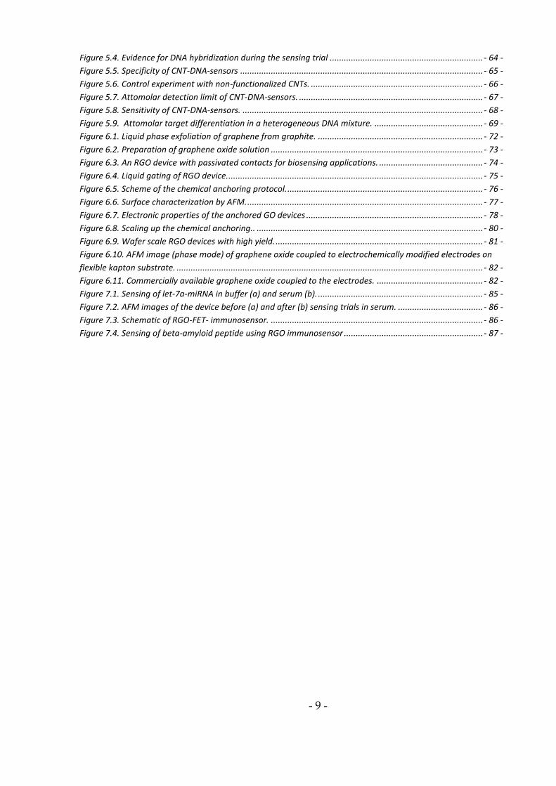
Figure 2.6. Various covalent functionalization schemes for graphene oxide. I: Reduction of GO II: Covalent surface functionalization of reduced graphene via diazonium reaction. III: Functionalization of GO by the reaction between GO and sodium azide. IV: Reduction azide–GO with LiAlH4 resulting in the amino-functionalized GO. V: Functionalization of azide–GO through click chemistry. VI: Modification of GO with long alkyl chains by the acylation reaction between the carboxyl acid groups of GO and alkylamine. VII: Esterification of GO by DCC chemistry or the acylation reaction between the carboxyl acid groups of GO and ROH alkylamine.VIII: Nucleophilic ring-opening reaction between the epoxy groups of GO and the amine groups of an amine-terminated organic molecules (RNH2). IX: The treatment of GO with organic isocyanates leading to the derivatization of both the edge carboxyl and surface hydroxyl functional groups via formation of amides or carbamate esters (RNCO) [93].
Various thermally activated addition reactions for graphene and the sidewalls
of CNTs are available. Figure 2.7 collects different routes for the covalent
modification of carbon surface using addition reactions [102].

2. Carbon nanostructures for biosensing
- 27 -
Figure 2.7. Addition reactions for the functionalization of the carbon nanotube
sidewall [102].
As in the case of oxidized carbon nanostructures the products of the addition
reactions are often used for subsequent attachment of the receptor molecule. For
instance, fluorine in fluorinated CNTs can be replaced by nucleophilic substitution
using alcohols, amines, Grignard reagents or alkyl lithium compounds [102].
Photochemical activation was also implemented for modification of CNTs and
graphene. For instance, CNTs have been osmylated using osmium tetroxide (OsO4)
under UV light irradiation [104]. Similarly, under intense UV-irradiation graphene
can react with benzoyl peroxide [105].
Electrochemical functionalization provides the attachment of biomolecules on to
carbon surfaces in a very versatile manner in a covalent or non-covalent fashion [106,
107]. For performing electrochemical reactions an electrochemical cell is used. A
typical electrochemical cell consists of a working electrode (WE), a reference
electrode (RE) and a counter electrode (CE). The working electrode provides the
surface for electrochemical reactions. When a positive overpotential is applied,
oxidation of an electrochemically active component in the solution can be achieved.
Negative overpotential may induce reduction processes. RE is used to set the
reference potential and CE is important for monitoring the electrical current
generated in the cell during the electrochemical process. Both covalent and non-
covalent modification can be realized, for instance, by using receptor molecules

2. Carbon nanostructures for biosensing
- 28 -
containing aminophenyl groups (Figure 2.8) [108]. If CNT is used as a working
electrode, application of positive voltages leads to polymerization of the molecule on
the CNT surface forming a uniform functional layer. In order to functionalize
nanotubes covalently aminophenyl moieties should be first converted into its
diazonium salt which is very reactive. Electrochemical reduction causes the
formation of aryl radical which can be coupled to the nanotube wall.
Figure 2.8. Schemes for (a) oxidative ECM with 4-aminobenzyl-R and (b) reductive ECM with an aryl diazonium salt. In the former case, the modified SWNT is covered by a polymeric layer of aminobenzyl groups without the formation of a chemical bond, whereas in the latter case, polyphenyl groups covalently attached to the nanotube are formed [108].
Electrochemical modification (ECM) is a very fast and efficient method for
the modification of carbon nanostructures. It can be easily upscaled and automated.
ECM ensures the coupling of the receptor selectively on the surface of transducing
component. This is essential for achieving low limit of detection. Due to these
reasons ECM was chosen as a strategy for the functionalization of CNTs in this work.
Experimental section
3. Fabrication of CNT-based sensors
3.1. Introduction. CNTs are shown to be promising for various
fields of use. A lot of possible applications including electrical sensing require
integration of CNTs into an electronic circuit. However, the fabrication of CNT
devices at the industrial level is still challenging [49, 109]. One of the most common
ways to integrate CNTs into a circuit is the writing of the metal contacts on randomly
deposited CNTs using e-beam lithography. However, this method is time-consuming
and requires manual operation for fabricating individual devices. CNTs can be
grown directly from catalyst particles deposited on the pre-patterned electrodes
[110]. This approach requires high temperatures and positioning of the catalysts at
the exact point. Another drawback of this method is the non-uniform growth of the
CNTs from each catalyst. Therefore up-scaling of mentioned technique seems very
difficult.
It is also very important to define the exact location of the final device on
the substrate from the beginning of fabrication process. This makes it possible to
assemble other parts of the sensor in a modular way. We used the dielectrophoresis
(DEP) technique to position the nanotubes at the desired location, for example, in
between platinum electrodes patterned on a substrate. This method offers
considerable advantages: it is fast, does not require expensive and bulky equipment
and can be automated and upscaled [111, 112]. To perform dielectrophoretic trapping
it is necessary to solubilize CNTs. After the DEP trapping and visualization, the
electrodes are passivated with an insulating layer and subsequently the nanotubes
are modified with receptors specific to certain analytes. The details of fabrication are
outlined in this chapter.
3.2. Preparation of CNT dispersions. Hydrophobic and strong
van der Waals interactions between the carbon nanotubes make it difficult to

3. Fabrication of CNT-based sensors
- 30 -
suspend them in water or other polar solutions. Some organic solvents (N,N-
dimethylformamide (DMF), dichloroethane), surfactants (sodium dodecyl sulfate
(SDS), sodium dodecyl benzene sulfonate (SDBS), etc) and polymers (nafion, DNA)
were shown to be efficient for nanotube solubilization [113-115].
Purification is another important aspect during the preparation of CNT
dispersion. SWCNTs powder contains a number of impurities (amorphous carbon,
catalysts, nanoparticles, etc) that might affect the quality of devices [116]. Gas phase
oxidation is often used to improve the homogeneity of CNTs [117]. To purify the
CNT solution standard purification techniques, like centrifugation, filtering, etc can
be used [116, 118]. Density gradient ultracentrifugation and gel-chromatography are
shown to be efficient techniques to separate SWCNTs with different chiralities from
their dispersions in surfactant. The solutions prepared using these approaches are
enriched with the nanotubes of only a certain physical structure. However the length
of the nanotubes in the resulting suspensions is less than 1 μm [119-122]. Therefore
these solutions are not very suitable starting material for the fabrication of devices
based on individual nanotubes.
We used 0.1% Triton X-100 aqueous solution for dispersing of the
SWCNTs. A small amount of CNT powder (HipCO oxidized) was added to
surfactant solution and dispersed with the help of ultrasonic agitation (Tip sonicator
HD-3100) for 40 sec with 1 sec impulse and 2 sec rest intervals. Ultrasonic cavitation
helps to overcome the bonding forces between the nanotubes, and separate them.
After that the SWCNTs dispersion was centrifuged (Rotanta 460 RS, Hettich) at 4637
g (4600 rpm) for 30 min, and the supernatant was filtered using filter paper [123].
Hexane extraction was used for further purification of the solution. This approach
allows the removal of hydrophobic impurities and undispersed CNTs from the
solution. Well-dispersed nanotubes due to the surfactant covering their surface
remain in aqueous phase. For the extraction equal volume of hexane was added to
CNT solution, mixed well and centrifuged for 5 min at 4600 pm. Upper hexane
fraction containing impurities is carefully separated from the clear CNT solution. The
CNT suspension prepared in this manner is not stable for long time, therefore some
processing steps, like short sonication and centrifugation, of older solution (more
than 1 week) are required before usage.
3.3. Visualization of CNT devices. Visualization of the
carbon nanotube devices is important for the optimisation of fabrication steps and
sensing conditions. Atomic force microscopy (AFM) is the most commonly used
technique for visualization of CNT devices. It gives an idea about the geometry of the

3. Fabrication of CNT-based sensors
- 31 -
electrodes and nanostructures, diameter and number of the trapped nanotubes or
bundles and the cleanliness of the surface. For the same purpose electron microscopy
can also be used. However imaging of SiO2 surface with scanning electron
microscope (SEM) requires its coating with a conducting layer to prevent
accumulation of electrostatic charge during electron irradiation. Therefore the
devices cannot be used after imaging. The resolution of optical microscope does not
allow the imaging of single CNTs or small bundles.
We designed a new method for the CNT visualization using fluorescent
dyes. CNTs have the ability to quench fluorescence of fluorescent dyes [124,125]. By
covering the sample with a thin layer of Rhodamin B (RB) it was possible to image
the CNTs on the SiO2 surface using a confocal microscope (TCS SP2, Leica). It is
apparent that the thin nanotube bundle (Figure 3.1.) can be clearly visualized due to
the efficient quenching of the dye fluorescence by complex formation with the
nanotubes [105]. Since confocal microscope imaging is much faster than AFM, this
approach can be used for a quick characterization of the sample. However it is not
possible to obtain information about the CNT diameter as it can be done using AFM.
Therefore all the devices used for this work were characterized using AFM - (Digital
Instruments Dimension IV, Veeco).
Figure 3.1. Visualization of the same SWCNT device with AFM and confocal microscopy: AFM (a) and confocal fluorescence (b) images of the same sample showing a tube trapped across electrodes. The confocal image was recorded after leaving the sample in a solution of RB in ethanol. RB complexes to the nanotubes and hence the fluorescence is quenched along the tubes. This helps in the clear visualization of the tubes on a substrate [123].

3. Fabrication of CNT-based sensors
- 32 -
3.4. Dielectrophoretic manipulation of CNTs.
Dielectrophoresis enables the positioning of CNTs at the desired location. It can also
be used for parallel assembly of 1D-nanostructures for fabrication of an array of
devices over a large wafer. By varying parameters of trapping it is possible to control
the density of nanotubes on the substrate surface. To understand what the variable
dielectrophoresis parameters are, it is important to know the nature of
dielectrophoretic force and factors that influence it.
3.4.1. The theory of DEP. Dielectrophoresis is an electrokinetic motion
of dielectrically polarized materials in non-uniform electric fields [126]. The
polarized object can move toward or away from the high field region depending on
the complex dielectric permittivity of the object with respect to its surrounding
medium. The CNT assembly process is conceptually illustrated in Figure 3.2. When
nanotube in the solution is located within the AC electric field, it polarizes. The
dielectric constant of the nanotube is larger than dielectric constant of the solvent.
This gives an origin to a positive DEP force. The CNT at kHz to MHz frequencies
gets attracted to the place where field is the strongest – to the tip of the electrode. The
CNT assembly process depends on the relative balance of the dielectrophoretic,
hydrodynamic and electrostatic double-layer interactions between the nanotube and
surface [127].
Figure 3.2. Schematic of the dielectrophoretic manipulation of 1D-nanostructures.
The dielectrophoretic force on a carbon nanotube assuming it to be a
cylindrical particle can be described by the following equation:
Where εm – relative permittivity of medium, r,l – radius and length of the
nanotube respectively, E – the local electric field, C – real part the dipolar

3. Fabrication of CNT-based sensors
- 33 -
Clausius-Mossotti factor. For an elongated object with the long axis aligned with the
field fCM is given by:
[
]
where and
are the complex permittivity of the CNT and surrounding
medium, respectively [128]. The complex permittivity is defined as ε*=ε-j(σ∕ω),
where ε is the permittivity, σ is the conductivity, and ω is the angular frequency of
the applied electric field, √ .
In agreement with the abovementioned equations for a certain type of
particle in a given medium one can tune the dielectrophoretic force by varying the
amplitude and the frequency of the applied electric field. The amount of nanotubes
trapped at the electrodes will depend also on the quality and the concentration of
solution, the design of the electrodes and the deposition time.
3.4.2. CNT trapping results. In our case, the aim was to trap carbon
nanotubes between platinum electrodes on silicon/silicon oxide samples. Pt
electrodes were written using standard photolithography on 4mm x 4 mm or 6 mm x
30 mm Si/SiO2 substrates. Dielectrophoretic trapping was performed by applying a
field between the electrode and backplate of the substrate while a drop of the carbon
nanotube solution was placed on the surface around the electrode (Figure 3.3). After
a required time (typically 15 sec) the substrate was washed with acetone and
isopropanol and blow-dried. Subsequently the substrate was annealed at 250oC for 2
hours. After that the devices can be visualized and characterized electrically.
Figure 3.3. Schematic of the dielectrophoretic trapping setup. The trap waveform is applied between one of the electrodes and the backplate.

3. Fabrication of CNT-based sensors
- 34 -
Figure 3.4. Different electrode geometries used in this study. Optimal parameters for CNT trapping: a) 25Mhz, 10V, b) 10 MHz, 3V, c) 25 MHz, 10V, d) and e) 10 Mhz, 10 V. Schematic of the substrate chosen as the most suitable for sensing trials (f). The AFM images of the electrode gaps with trapped CNTs are shown on (d) and (e).
Different shapes and sizes of electrode gaps were tested for trapping the
CNTs and subsequent biosensing trials (Figure 3.4). Geometry of the electrodes as
well as properties of the substrate strongly influence the dielectrophoretic trapping
of CNTs. Therefore the parameters had to be optimized in every case. Among
various electrode and sample designs the most suitable was chosen during the initial
sensing trials. Most of the sensing results described in this thesis were obtained on
the 6 mm x 30 mm Si/SiO2 samples with two pairs of platinum electrodes. The
geometry of the gaps for this kind of samples is shown in Figure 3.4 (d, e). In contrast
to samples of smaller sizes (4mm x 4 mm), liquid manipulation is much easier on the
chosen larger size samples since it makes it possible to integrate microfluidic channel
or reservoir for analyte solutions on top of the substrate. The DEP parameters used
for chosen samples were the following: 10 MHz, 10V, 15 sec.
3.4.3. Scalability of DEP. The possibility to scale-up dielectrophoretic
trapping of CNTs was subsequently investigated. For this purpose parallel
connection of the electrodes and common backplate were used for applying the AC
voltage. In this manner the dielectrophoretic force was generated simultaneously at

3. Fabrication of CNT-based sensors
- 35 -
all connected electrodes and the nanotubes were trapped concomitantly at several
positions (Figure 3.5).
Figure 3.5. One of the possible ways to upscale the DEP trapping of CNTs. a) Schematic of the trapping procedure. b) AFM images of four devices on the chip after a single trapping step.
Another way to scale up the trapping is by using a different configuration
of the electrodes. In this case the DEP force can be applied between the connected
microelectrodes on the substrate and a (quasi)-reference electrode (for instance
platinum wire). The advantage of this approach is that metalized backplate as well as
connecting additional electrodes on the surface are not required. Therefore it is
possible to fabricate CNT devices not only on Si/SiO2 samples, but also on glass and
flexible polymer substrates.
3.4.4. Monitoring the trapping of CNTs during DEP. For
optimizing the parameters of DEP it is reasonable to monitor the trapping by
measuring the impedance between the electrodes. It helps to control the resistance of
the device and thereby the density of nanotubes during the trapping itself. This

3. Fabrication of CNT-based sensors
- 36 -
configuration allows disconnecting the trapping field as soon as a trapping event
occurs. The value of the impedance directly provides us with a measure of the
density of nanotubes.
The impedance monitoring technique is implemented by superimposing
two AC waveforms: a trap waveform (10 V at 25 MHz) between one Pt electrode and
the backplane of the substrate and a probe waveform (10 mV at a lower frequency 2623
Hz) between the two Pt electrodes to monitor the trapping event (Figure 3.6 a). The
trap waveform is supplied by a function generator (Agilent 33250A) and the
impedance is recorded at the frequency of the probe waveform using an Agilent
E4980A LCR Meter.
Figure 3.6. Monitoring the dielectrophoretic trapping of the nanotubes. a) Schematic of the experimental set-up used to monitor the dielectrophoretic trapping of nanotubes. The trap waveform is applied between the drain (D) electrode and the backplate, while the impedance is monitored across the drain and the source (S) electrode using the probe waveform. b) In situ impedance monitoring during DEP trapping: the magnitude and phase of the gap impedance are plotted as a function of time. A CNT suspension is first introduced (arrow) and ~10s afterwards clear steps can be seen indicating trapping events. (Inset: an AFM picture showing the trapped nanotubes across the gap). c) the magnitude and d) the phase of the impedance spectrum of the electrode gap in air before and after deposition, as well as after annealing.
Figure 3.6b shows a typical deposition sequence. Initially, the substrate is
in air and the system is purely capacitive with the impedance higher than 10 Ω and
a phase of -90°. A drop of CNTs is placed above the electrode gap. This leads to a
decrease in impedance to a few MOhm and a phase of -40°, due to the conductivity
3. Fabrication of CNT-based sensors
- 37 -
of the solution. After several seconds, trapping events are registered, which appear
as discrete steps both in the magnitude and phase signals. At this instance, the
impedance is just a few hundreds of kOhm and the phase close to zero suggesting
that CNTs are trapped (see inset AFM image). The sample is then washed with
acetone during which the trap waveform is still active. The washing procedure
introduces some changes in the impedance. Finally the sample is removed and
washed thoroughly with isopropanol.
A frequency of 2623 Hz of the probe waveform was chosen so that the
change in the signal between the empty situation and the trapped condition is
maximized with a good detection sensitivity and fast response time. The contact
resistances of the devices could be reduced by around an order of magnitude by a
subsequent rapid thermal annealing step at 650°C (45s) or a longer heating period
(2h) at 250°C in argon (Figures 3.6c and 3.6d). Online impedance monitoring can be
used either to actively control the amount of nanotubes trapped at a specific location
or as a way to calibrate the deposition time needed for a given nanotube suspension.
3.5. Passivation of electrodes. The chosen device architecture
is designed in such a way that it can be used in a liquid environment – for sensing
different analytes in serum or other biological liquids. These fluids contain a
significant amount of electrolytes that cause a background electrical current between
electrodes through the liquid. This ionic current is strong enough to affect sensing
results. Besides, electrodes can provide large surface for electrochemical reactions.
This can reduce reaction rate on the CNT surface during electrochemical
functionalization and increase the limit of detection. Some components of analyte
solution may also sediment non-specifically on the metal electrodes during the
sensing trials and cause changes in electrical response of the device. All these factors
make it important to ensure that CNT is the only conductive element that is exposed
to solution. To achieve this passivation of electrodes is required. The passivation
process should ensure robust and stable electrical isolation of electrodes on the areas
of substrates coming in contact with the liquid. It should have a minimal effect on the
electrical properties of CNTs. Furthermore, surface contamination during this
process has to be avoided.
In this work we have used a second lithography step to deposit 100 nm
titanium covered with 200 nm silicon oxide to passivate Pt microelectrodes near the
gap. For this purpose the substrate was spin-coated with a photoresist (ma-P 1215,
micro-resist technology GmbH) and baked for 2 min at 90oC to obtain a 1.5 μm thick

3. Fabrication of CNT-based sensors
- 38 -
layer. Absorption maximum of ma-P1215 is close to 365 nm and 415 nm. Exposure of
this resist to UV light causes chemical changes that increase the solubility of the
exposed areas. Illumination of this photoresist with visible light of up to 580 nm can
induce chemical changes. Using a confocal microscope (TCS SP2, Leica) the desired
areas were first localized with a high level of precision using low power illumination
by a 633 nm laser (imaging laser). Then the required areas were exposed using a high
power 476 nm write-laser [129]. Writing was performed by using a piezoelectric
stage with precise computer control for positioning and moving the sample.
Alternatively, a well aligned mask for exposing desired areas was also experimented.
In this case a mask-aligner is used for the precise positioning of the mask and
exposure of the required areas.
Figure 3.7. Passivation of Pt electrodes on Si/SiO2 surface. a) schematic of passivation, b) and c) AFM image of CNT device before and after passivation respectively.
Using a developer solution ma-D 331, the resist on exposed areas was
dissolved. After the washing with water and drying in nitrogen flow,

3. Fabrication of CNT-based sensors
- 39 -
100nmTi/200nmSiO2 was evaporated on the substrate. Such a combination of
metallic (Ti) and insulating (SiO2) layers gave the best results for keeping
conductivity of CNTs intact. Without the use of Ti a significant number of devices
lost their conductivity, which can be explained by the mechanical brakeage of CNTs
upon direct deposition of the silicon oxide layer. For removing evaporated layers
from the unexposed areas a lift-off in 1-methyl-2-pyrrolidone (55C for 3 h) was
performed. After this, samples were washed with acetone and isopropanol and blow-
dried. After the lift-off a thermal annealing of the samples (2 hours at 250oC or 45 sec
at 600oC in argon) was also carried out.
3.6. Chemical functionalization of CNTs. The discussed
above fabrication steps were aimed to obtain devices with high sensitivity. Another
important aspect for biosensors is selectivity. A biosensor should be sensitive mainly
to the molecule of interest. Other components of analyte solution should not cause
any significant sensor signal changes. As it was mentioned before (paragraph 1.2),
selectivity of the biosensor is provided by the biorecognition component of the
sensor which should be in high vicinity to transducing element. In our case, receptor
molecules should be immobilized onto the carbon nanotube.
Ideally the functionalization strategy should ensure that the receptor is
immobilized on the surface of CNT and not on the surrounding silicon oxide. This is
important for the efficient recognition and transduction processes and proper
interpretation of the signal changes. For example, using a spotting technique for
receptor immobilization can lead to significant amount of biorecognition events
happening on the surrounding silicon oxide surface but not on the CNT surface itself.
In this case, the limit of detection may be high. Electrochemical modification leads to
the attachment of the receptor to CNT surface only providing the basis for highly
efficient biosensor functioning. It is also possible to perform electrochemical reactions
inside the microfluidic channel when the biosensing system is fully assembled. This
strategy was used, for example, for the preparation of glucose-sensors.
As it was explained in paragraph 2.4 using electrochemistry it is possible to
modify CNT covalently and non-covalently. Covalent ECM has advantages due to
good homogeneity and stability of ligand distribution attainable on the nanotube
surface, coupled with a high signal to noise ratio. Non-covalent functionalization
does not affect the underlying electronic structure of the carbon nanotubes. Two
ways of electrochemical modification - covalent and non-covalent - affect the
electronic properties of CNTs differently. It was demonstrated using modification of
CNTs with boronic acid (BA) as an example. Boronic acid was used as a receptor for

3. Fabrication of CNT-based sensors
- 40 -
glucose sensing. 3-aminophenylboronic acid (APBA) was used as a precursor for the
modification. The functionalization is carried out according to Figure 3.8 [130].
In order to covalently attach the phenylboronic acid receptor to the
nanotube, a highly reactive diazonium radical is created. It binds to the nanotube via
reductive coupling. For this purpose, 5 mg of APBA was dissolved in 5 ml of 20mM
H2SO4. After this the beaker was put into an ice bath. 5 ml of 8mM HNO2 were added
slowly with continuous stirring to the reactive mixture. Shortly after the components
are mixed the solution starts to become yellow indicating the formation of diazonium
radicals [130].
Figure 3.8. Scheme showing the functionalization strategy to obtain the BA-CNT-sensors. For covalent attachment (top route), the phenyl boronic acid precursor is
converted into a reactive diazonium radical through diazotization at 4C. This cold solution is flushed through the microchannel and the electrochemical functionalization of the nanotube carried out under reductive conditions (-0.55 V vs. Ag/AgCl). For the non-covalent attachment (bottom route), the precursor is directly electropolymerized to obtain a polymer wrapping on the nanotube surface under oxidative conditions at room temperature [130].
The microchannel made of polydimethylsiloxane (PDMS) placed on the
chip is filled with a fresh diazonium solution and the voltage applied at the Ag/AgCl
reference electrode is swept between -0.1 V and +0.55 V. Correspondingly, the
voltage on the nanotube varies between +0.1V and -0.55V. The impedance of
nanotube device is monitored during the ECM. Figure 3.9 shows the changes in
magnitude and phase of impedance during the modification. During the five cycles
of voltage sweep the magnitude of impedance increases and the phase of impedance
decreases. The resistance value normally increased by a factor ranging from 1.5 to 2.

3. Fabrication of CNT-based sensors
- 41 -
Excessive covalent modification of CNT can lead to a complete loss of conductivity
due to damage of the nanotube structure [130].
Figure 3.9. Gate dependence of the devices during (a) covalent and (b) non-covalent electrochemical functionalization of CNTs with APBA. Arrows indicate the increase of resistance (black) and decrease of phase (blue) values during reductive coupling of boronic acid.
The diameter of the nanotubes also increases after the ECM. This was
observed in AFM images of the device before and after covalent functionalization.
The changes of CNT properties were also monitored using Raman spectroscopy. The
D-band of CNTs (which corresponds to Raman intensity peak at 1300 cm-1 frequency)
is associated with defects in the carbon nanotube structure. It is clear that during the
covalent attachment of the diazonium radical to the nanotube some of the native sp2
bonds of the CNT wall are destroyed to form a new bond. This can be observed as an
increase of D-peak in Raman spectra as it is seen from Figure 3.10 d.
Non-covalent attachment of the receptor was achieved via direct
electropolymerization of the APBA under oxidative conditions, by sweeping the
voltage at the nanotube from -0.1 V to +0.7 V versus Ag/AgCl in the ethanol solution
of 5mM APBA containing 100mM LiClO4. In this case the resistance increased only
slightly during the sweep (Figure 3.9 b). After functionalization, 10 mM H2SO4 and
water were flushed through the microchannel. The non-covalent coupling results in a
height increase of 3-5 nm as inferred from AFM measurements [130].

3. Fabrication of CNT-based sensors
- 42 -
Figure 3.10. Electrochemical functionalization of CNTs. AFM images of the device before (a) and after (b) covalent modification of CNTs with APBA and corresponding height profiles (c) show increase of the nanotube diameter. Raman spectra before and after modification (d) showing a clear increase in the D-band intensity signifying the formation of covalent bonds with the BA moieties.
3.7. Sensing strategy. Impedance measurements at different gate
voltages were taken for the detection of biomolecules. The impedance (Z, a complex
quantity with magnitude and phase) was measured using an impedance analyzer
(Agilent 33250A LCR Meter) in a frequency range of 20 Hz to 2 MHz. Using an AC
signal to record the sensor characteristics improves the signal-to-noise ratio and
reproducibility compared to a DC measurement while enabling acquisition of both
the magnitude and phase spectra of the sensor. This frequency response is measured
at varying gate voltages to characterize the field-effect behavior. The gate voltages
are maintained in the range of -0.4 V to 0.4 V (at the Ag/AgCl reference) [130].

3. Fabrication of CNT-based sensors
- 43 -
The resulting dataset can be visualized in the form of a magnitude map as
shown in Figure 3.11. The X-axis corresponds to the liquid gate voltage, while the Y-
axis indicates frequency. Every point in the image corresponds to the magnitude of
impedance at a certain frequency and gate voltage. It is possible to derive both
frequency- and gate-dependence from such kind of measurement. Therefore 2D Z-
maps contain the complete electrical characteristics of the sensor and can be used to
probe their transduction mechanism in detail.
Figure 3.11. Detection strategy: a) ZMagnitude-2D-map, b) schematic of a liquid gated CNT-FET, c) frequency dependence of magnitude of impedance at fixed gate voltage 0V, d) gate-dependence of magnitude of impedance at fixed frequency 100 Hz.
Most of the devices obtained in described way show a semi-metallic
transport behavior with a gate modulation of less than an order of magnitude,
signifying the predominant presence of metallic tubes. Due to the low density of
states around the Fermi level, metallic nanotubes show a slight gate modulation [131]
and are hence suited for field-effect based detection [107]. Unlike other FET-based
sensors, which require semiconducting materials, our AC measurement strategy
coupled with the use of a stable reference electrode enables the use of metallic tubes

3. Fabrication of CNT-based sensors
- 44 -
as detectors. Another advantage of using metallic nanotubes lies in their low
resistance in the kΩ range, which facilitates improved sensor signals in comparison
to their semiconducting counterparts [130].

4. Sensing of saccharides
4.1. Introduction. Carbohydrates are important biomarkers for
different diseases. The most common example of them is glucose as a marker for
diabetes [132]. Glucose sensors mostly rely on the use of an enzyme such as glucose
oxidase (GOx) or glucose dehydrogenase to generate redox mediator species, which
are thereafter detected electrochemically [133]. These sensors require the coupling of
the enzyme in close proximity to the transducing electrode to obtain high sensitivity.
CNTs have also been employed as electrode material in electrochemical sensors for
glucose [61, 134]. While providing good selectivity to glucose, such sensors rely on
the rate of reaction between the enzyme and glucose and hence are inherently
sensitive to factors influencing enzyme activity. In addition, the limited stability of
the immobilized enzyme may restrict the shelf life of such sensor systems and their
application for in vivo glucose monitoring [135]. Apart from electrochemical
transduction, field-effect based detection has also been presented using a CNT-GOx
sensor [40]. However, the sensing mechanism and concentration dependence were
not discussed there [130].
During the last decade there is a tremendous amount of research directed
towards the realization of non-enzymatic glucose sensors [136]. One major approach
involves the direct oxidation of glucose at nanostructured electrodes [137-139]. The
nanostructuring allows the detection of glucose at a lower overpotential [140].
However, such electrodes are very sensitive to adsorbed interferents such as the
amount of chloride and suffer from surface fouling over longer times [130, 141, 142].
An alternative enzymeless approach for glucose detection involves the use
of fully synthetic receptors such as boronic acid (BA) containing compounds. BA
binds reversibly with cis-1,2- and cis-1,3-diols to form five- and six-membered cyclic
esters respectively [143, 144]. Based on this, fluorescence sensors, [145, 146],
potentiometric / amperometric sensors [147, 148] and recently a field-effect based
sensor [149] have been demonstrated. The chemical structure of the boronic acid
receptor can be optimized to obtain highly selective and sensitive affinity-based
glucose sensors [145]. In addition to glucose, free carbohydrates as well as their
conjugates such as liposaccharides and glycoproteins are also important in the
diagnosis of pathological states such as cancer [150]. While enzyme-based sensors are
not directly amenable for the detection of bound saccharides, an affinity-based sensor

4. Sensing of saccharides
- 46 -
can potentially be deployed for the detection of both free and bound forms of these
molecules [130, 151, 152].
In contrast to enzymatic sensors, the detection principle here is based on
complexation, which is a reversible, equilibrium-based reaction without the
consumption of the analyte. So the present sensor does not rely on enzymes or
electrochemical redox mediators to function but rather on a combination of affinity
sensing and the field effect transistor (FET) effect. Glucose detection with BA-CNT
device was chosen to be a model for investigation of the sensing mechanism in
presented biosensor configuration [130].
4.2. Device fabrication. The details of device fabrication were
described in previous chapter. As it was mentioned there, the control of the kind of
chemical coupling (covalent or non-covalent) between the boronic acid receptor and
the nanotube was achieved using electrochemical modificaton. The first attempts to
detect glucose using boronic acid functionalized CNTs were performed in an open
system without the application of liquid gate voltage, by measuring the impedance
spectra of the device before and after its exposure to analyte solution (Figure 4.1a).
This configuration was discarded due to significant amount of aggregates on the
surface of the sensor as observed using an AFM (Figures 4.1b and 4.1c). These
adsorbates affect the quality of sensing and as an outcome no reproducible and
reliable results were achieved. In later investigations the contamination of the SiO2
surface could be eliminated when the measurement was performed using
continuously applied liquid gate voltage. The sample dimensions and design were
therefore changed in order to allow better manipulation of liquids and easier
integration of the gate electrode.
Figure 4.1. Sensing in the open system without applying liquid gate voltage: photo of the integrated chip with the drop of analyte solution (a), AFM image of the device before (b) and after (c) sensing trials.

4. Sensing of saccharides
- 47 -
Liquid handling was improved by using a microfluidic channel connected
to a flow-control system. For the microfluidic fabrication polydimethylsiloxane
(PDMS) was used to prepare 2 mm thick plates with a 30 µm channel. The degassed
mixture of PDMS and curing agent (PDMS: Sylgard 184, 10:1 ratio) was poured on a
SU-8 mold and baked at 65oC for 1 h. The sample was then placed on the chip-carrier,
wire-bonded and covered with the PDMS and glass plates, so that the nanotube
devices were integrated into the microchannel (Figures 4.2b and 4.2c). The flow of the
solutions was regulated using a computerized pressure-based flow control system
(MFCS-4C, Fluigent). An Ag/AgCl reference electrode placed in contact with the
liquid in the microfluidic circuit allows us to set the potential precisely on the surface
of the nanotube. This electrode serves two purposes namely as a reference electrode
for electrochemical functionalization and as a gate electrode for measuring the FET
characteristics. The Ag/AgCl reference that acts as a gate electrode is placed in the
waste reservoir that is connected to the outlet [130].
Figure 4.2. (a) An AFM image of the electrode region of a BA-CNT sensor after the sensing trials The SiO2 passivation layer can be seen extending above both electrodes. (b) A schematic representation of the microfluidic set up with the location of the nanotube device. The channel is carved out in the PDMS layer and the nanotube device is directly below the channel on the substrate. (c) a photograph of the final assembled device [130].

4. Sensing of saccharides
- 48 -
4.3. Sensing results. The sensing trials were performed using the
measurement strategy described in the previous chapter on more than 10 devices
using varying concentrations of glucose solutions in 10 mM phosphate buffer (pH
8.4). First the sensing response of the covalently coupled BA-CNT devices will be
discussed.
Figure 4.3. Affinity sensing of saccharides: binding of diol to boronic acid-functionalized carbon nanotube at a pH of 8.4. The formation of the ester leads to an increase in the relative negative charge at the surface of the nanotube which can be detected electrically. The reaction is reversible at low pH. In an acid solution at a pH of around 4, the attached saccharide can be released going back to the initial state [130].
4.3.1. Sensitivity to glucose. The general idea behind the functioning
of the sensor is shown in Figure 4.3. The binding of glucose to the attached BA
receptors leads to a change in the net charge distribution on the nanotube surface,
which can be sensed through changes in the impedance of the nanotube. The Z-maps
of a typical sensor in buffer and in glucose are shown in Figures 4.4a and 4.4b
respectively. The magnitude plots show subtle differences in the low frequency
region. These variations are further apparent in the cross-section profiles collected in
Figures 4.5a and 4.5b. These section profiles are extracted from the 2D Z-maps by
plotting either the frequency response at a fixed gate voltage or the gate dependence
at specific frequencies. From the magnitude spectrum in Figure 4.5a it is apparent
that at low frequencies, the device acts as a resistor, while capacitive effects become
dominant as the frequency increases. The resistance of the device shows nominally a
5% increase upon binding of glucose, as is apparent in Figure 4.5a. The increase in
resistance can be attributed to stronger scattering centers due to the increase in net
charge when glucose binds to the receptor sites on the nanotube (Figure 4.3). This
mechanism is consistent with the occurrence of analyte dependent carrier scattering
[41]. Further support for the scattering based sensor response is obtained from the

4. Sensing of saccharides
- 49 -
gate voltage dependence in Figure 4.5 (b), where it is apparent that the higher
resistance persists over almost the entire gate voltage range.
Figure 4.4. 2D-impedance (Z-) maps showing the impedance as a function of frequency and liquid gate voltage. Magnitude [Ohms] maps of the impedance of covalently functionalized BA-CNT devices are shown in buffer (a) and in 10 mM glucose (b). Subtle changes in the impedance response can be clearly seen upon exposure of the sensor to glucose as indicated by the twin-headed black arrows [130].
To measure the concentration response of covalently modified BA-CNT,
the devices were exposed to successive aliquots of a 5 mM glucose solution. A 1 µL
aliquot of the analyte solution was flushed over the sensor at a precise speed,
followed by 9 µL of buffer solution at which point the flow was stopped and the
impedance measured. This cycle was repeated several times. The Z-maps for the
various injections are collected in Figure 4.6a.
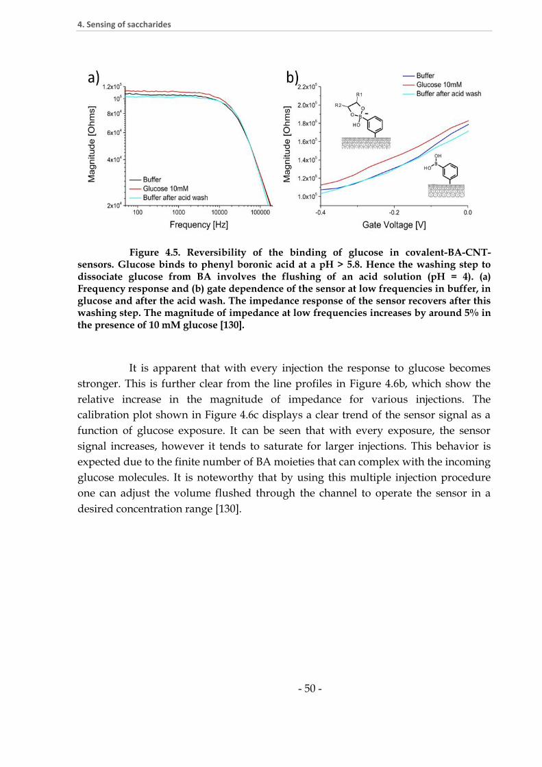
4. Sensing of saccharides
- 50 -
Figure 4.5. Reversibility of the binding of glucose in covalent-BA-CNT-sensors. Glucose binds to phenyl boronic acid at a pH > 5.8. Hence the washing step to dissociate glucose from BA involves the flushing of an acid solution (pH = 4). (a) Frequency response and (b) gate dependence of the sensor at low frequencies in buffer, in glucose and after the acid wash. The impedance response of the sensor recovers after this washing step. The magnitude of impedance at low frequencies increases by around 5% in the presence of 10 mM glucose [130].
It is apparent that with every injection the response to glucose becomes
stronger. This is further clear from the line profiles in Figure 4.6b, which show the
relative increase in the magnitude of impedance for various injections. The
calibration plot shown in Figure 4.6c displays a clear trend of the sensor signal as a
function of glucose exposure. It can be seen that with every exposure, the sensor
signal increases, however it tends to saturate for larger injections. This behavior is
expected due to the finite number of BA moieties that can complex with the incoming
glucose molecules. It is noteworthy that by using this multiple injection procedure
one can adjust the volume flushed through the channel to operate the sensor in a
desired concentration range [130].

4. Sensing of saccharides
- 51 -
Figure 4.6. Concentration dependence of the covalent-BA-CNT-sensors. a) Z-maps in the absence of glucose (0) and after 1, 4 and 6 injections of 5 mM glucose. Scale: 20 kOhm – 40 kOhm. Every injection comprises of a 1 µL aliquot of 5 mM glucose followed by a 9 µL aliquot of buffer solution, at which point the impedance response is acquired. b) The plot shows the relative change in the magnitude of impedance glucose injections. c) Calibration curve plotting the relative % change as a function of glucose exposure showing clear concentration dependence. The actual amount of glucose can be read from the top Y-axis [130].
Control experiments were performed with CNTs that were not
functionalized. Figure 4.7 shows the gate- and frequency dependences of such
devices initially and after exposure to glucose. No significant changes were observed
in this case [130].

4. Sensing of saccharides
- 52 -
Figure 4.7. Control experiment with unmodified CNT devices. A non-functionalized CNT shows negligible changes in its response when exposed to glucose as can be seen from the (a) gate voltage scans and (b) frequency responses [130].
4.3.2. Response to other monosaccharides and interferents. As
it was mentioned before (paragraph 4.1), boronic acid is not a specific receptor for
glucose. It can bind other saccharides as well. The detection of fructose binding was
demonstrated using the presented BA-CNT sensor. As it is seen from Figure 4.8, the
response of the sensor to fructose was similar to the glucose case. Furthermore, the
response was reversible as is apparent in the recovery of the signal after the acid
wash.
Electrochemical glucose sensors suffer from the interference of other
substances that may be present in body fluids. Among such interfering molecules is
acetaminophen [133]. The sensor response on the presence of acetaminophen was
evaluated here (Figure 4.8). It is apparent that acetaminophen did not cause signal
change of BA-CNT sensor for glucose. This is expected since the BA moieties exhibit
a high degree of selectivity to saccharides [130].

4. Sensing of saccharides
- 53 -
Figure 4.8. Selectivity of the covalent BA-CNT-sensors. The BA-CNT sensors presented here are not sensitive to interferents that are common for enzymatic sensors. Here the case of acetaminophen is presented. The BA-CNT sensor shows negligible response when exposed to a solution of acetaminophen (even at a high concentration of 10mM) as can be seen from the (a) gate voltage scans and (b) frequency response [130].
4.3.3. Sensing mechanism. In order to elucidate the sensing
mechanism it is important to understand the physico-chemical phenomena
responsible for the impedance changes brought by exposure to glucose. For this
purpose, the reversible binding of boronic acid to glucose on the surface of CNTs
must be presented first. A schematic of this equilibrium can be seen in Figure 4.9. In
the absence of glucose, the neutral (1) and negatively charged (2) forms of the
attached phenyl boronic acid exist in equilibrium with a certain pKa (pKa1 ≈ 8.8)
[153]. cis-1,2- and cis-1,3-diols complex with boronic acid at pH > 5.8 to form cyclic
esters. The complexed forms (3 and 4) have a pKa (pKa2 ≈ 6.8) that is lower than that
of the free BA [153, 155]. Thus all the four species are in equilibrium leading to a net
charge on the complexed or non-complexed BA species depending on the pH (Figure
4.9). In order for the sensor to detect the binding of glucose, there should be some
difference in the net charge before and after binding [130].

4. Sensing of saccharides
- 54 -
Figure 4.9. Charge distribution on the surface of BA-functionalized CNTs calculated using the Henderson-Hasselbach relationship. The black curve corresponds to the case without glucose, while the red curve represents the situation with glucose. (pKa1 ~ 8.8, pKa2 ~ 6.8). The cyan-colored vertical line corresponds to the working pH of 8.4. Refer to text for further details [130].
Based on this, the optimal working pH would be the one that has a value
between pKa1 and pKa2. Due to this reason, the working pH was chosen to be 8.4. At
this pH (marked by the vertical line), the relative charge on the complexed species is
maximized with respect to the charge on the unbound species. In other words, at this
pH, 1 and 3 are expected to be the dominant species before and after complexation
respectively. As a result, the net charge on the surface of the CNT is relatively higher
in the presence of glucose in comparison to the situation without glucose. It is
noteworthy mentioning here that the exact values of pKa1 and pKa2 of the BA-CNT
assembly might be slightly different from the known values. However, this would
only shift the black and red curves slightly reducing the difference in the net charge
by a small amount. Based on this picture, it can be concluded that the increased
charge on the covalently attached BA centers in the presence of glucose leads to a
stronger scattering of charge carriers resulting in a higher resistance [130].

4. Sensing of saccharides
- 55 -
While the consistent increase in resistance for a broad gate voltage range
and its clear concentration dependence strongly support the scattering mechanism
related to changes of charge carrier mobility, two other mechanisms also deserve
attention as has been postulated for semiconducting CNTs [41, 155]. The first one
concerns an alternative effect of the analyte dependent change in charge on the
nanotube surface namely a threshold voltage shift, analogous to the working
principle of an ion-selective field-effect transistor (ISFET) [156]. In a second scenario,
the docking of analytes on the nanotube surface could lead to an increased screening
of the gate potential by an increase in the thickness or a change in dielectric constant
of the receptor coating. This would alter the effective gate capacitance, which would
result in a change in the slope of transconductance characteristics, signifying a
modulation of the gate coupling coefficient [41, 130].
Non-covalent attachment of the receptor does not alter the electronic
structure of the CNT. Therefore this kind of functionalization is preferred for
evaluation of these two mechanisms of sensing – threshold shift and change of
capacitive coupling. As it was described previously (paragraph 3.6), through
electropolymerization phenyl boronic acid moieties were attached in a non-covalent
manner to obtain coatings of 3 nm thickness. Figures 4.9a and 4.9b show the
ZMagnitude-2D-maps for the non-covalently functionalized BA-CNT device in
buffer and in a 10 mM glucose solution. It is apparent that the behavior in glucose is
quite different from that of the covalent-BA-CNT case, with the device having a
higher resistance at negative gate voltage and a lower resistance at positive gate
voltage and thus a markedly different slope of the gate-dependence of the
conductance (Figure 4.9c). The reduction in slope signifies a less efficient coupling of
the liquid gate. This can be explained by change in the polymer layer - increased
dielectric shielding arising from bound glucose moieties on the BA layer.
Furthermore, at working pH of 8.4, the bound glucose moieties on the
thick BA layer must have an average net charge higher than in the free BA condition,
as discussed in Figure 4.9. That is indeed the case as can be inferred from the curve
shown in Figure 4.10d (obtained after the correction for slope change), where clear
thresholds shift can be extracted. For the sample in Figure 4.10, we calculated this
shift to be around 24 mV. Similar values (in the range of 10 – 30 mV) have been
obtained on other devices [130].

4. Sensing of saccharides
- 56 -
Figure 4.10. Sensor response for non-covalent-BA-CNT devices showing the gate dependence of the magnitude of impedance at low frequencies. ZMagnitude -2D-maps before (a) and after (b) glucose exposure. c) coupling efficiency (characterized by the slope of transconductance) of the sensor before and after exposure to a 10 mM glucose solution. d) threshold voltage calculation after correction of the coupling efficiency (c and d are derived from ZMagnitude-2D-maps). In (c), it can be seen that in the presence of glucose the coupling (slope) is lower, while in (d) the binding of glucose to BA moieties shifts the threshold voltage [130].
It could be argued that the sensor responses for the covalent case could
also be explained using these two mechanisms similar to the non-covalent scenario.
However, there are a number of arguments, which speak against this possibility.
First, the moieties that are covalently attached are very and hence the screening effect
if present is expected to be very minimal. Furthermore, since we have more than one
tube across the electrodes, it is unlikely that the sparsely distributed charge centers
can bring in a significant threshold voltage shift in the gate characteristics. Finally,
the gate dependence of resistance in the presence of glucose shows an increase in

4. Sensing of saccharides
- 57 -
resistance for all gate voltages in a number of covalent-BA-CNT samples, strongly
supporting the previous arguments [130].
4.4. Conclusions. In conclusion, using a novel type of non-
enzymatic glucose sensor based on carbon nanotube devices site-selectively
positioned in microfluidic channels the mechanisms of sensing where investigated.
By a control of the nature of coupling between the receptor and the nanotube, it was
possible to elaborate on the various transduction mechanisms with the help of the
impedance detection technique. The sensitivity can be further increased by the use of
appropriate receptors that provide a higher binding constant for glucose. The
presented sensors are compact and show promise for applications such as in vivo
glucose monitoring.

5. Label-free detection of few copies
of DNA
5.1. Introduction. The detection of specific nucleic acid sequences
plays a vital role in environmental, food and clinical monitoring and in forensic
screening. Deoxyribonucleic Acid (DNA) hybridization is the basis for the detection
of various infections and genetic disorders [157, 158]. On the other hand, the
detection of messenger RNA (mRNA) is important for applications such as in the
estimation of the gene expression level [159]. The introduction of real-time
polymerase chain reaction (RT-PCR) [160] and microarrays [161] have revolutionized
the way in which nucleic acid assays are implemented, enabling the highly sensitive
detection of various biomarkers. In all these methods, the target DNA is amplified,
which is a prerequisite for obtaining high sensitivity [162]. Furthermore, microarray-
based detection requires a labeling step, which affects the time, efficiency and the
total costs involved in the complete detection protocol. The ability to detect few
copies of unlabeled DNA without the need for a bulky optical reading instrument
will pave way for the facile entry of nanoanalytical devices for point-of-care
diagnostics [163]. Sensors based on hybridization of nucleic acids constitute the basis
for today’s molecular diagnostics [164]. Such sensors find application in the detection
of various diseases, depending on the presence or absence of specific nucleotide
sequences. Current methods are able to identify few copies by amplifying the sample
using PCR to obtain a detectable amount of DNA [165]. For applications involving
comparison of gene expression levels, microarrays are used [166]. This requires the
labeling of the target sequences to enable their subsequent detection using a
fluorescence microscope [167].
Label-free electrical detection of DNA has been demonstrated in a variety
of configurations [168]. The majority of them are based either on field-effect detection
[18, 60] or on electrochemical detection [169]. 1D-nanostructures were used for
improving the limit of detection of DNA assays. For example, electrochemical GaN
nanowire-based DNA detection was performed by monitoring electrochemical peak
of guanidine oxidation. In this case the authors could reach sub-pM level of DNA
detection [170]. Gold nanowires functionalized with PNA were used for
electrochemical detection of mRNA with the help of catalytic reporting. This sensor

5. Label-free detection of few copies of DNA
- 59 -
showed sensitivity up to 100 fM RNA [171]. The best detection limit reported until
now based on silicon nanowires is 10 fM [172, 173]. However, silicon nanowires
suffer from extremely high resistances (in the gigaohm range), which sets a limitation
on the achievable sensitivity [156]. Almost all of the silicon nanowire sensors are
based on resistive detection without the use of a reference electrode. While this is
useful in the demonstration of prototype sensors, the use of a reference electrode is
unavoidable when one requires stability and reproducibility of the sensors [18, 174,
175]. Therefore using a CNT as sensitive element and a reference electrode to set a
stable potential can bring significant improvement in the field of DNA electrical
sensors. Some results on CNT-based electrical DNA detection were already
demonstrated by other groups. However a significant improvement of the limit of
detection was not achieved there. In comparison to state-of-the-art field-effect
sensors based on carbon nanotube networks [66], the sensor presented here shows up
to 5 orders of magnitude improvement in the detection limit.
5.2. Sensing setup. For DNA sensing the sample with CNT device
prepared as described previously (Chapter 3) was attached to chip-carrier and wire-
bonded.
Figure 5.1. Overview of the assembled carbon nanotube DNA sensor. (a) Photo showing the chip-carrier (printed circuit board) with the wire-bonded sensor chip covered with a PDMS layer. The sensor chip contains Pt electrode gaps (b), where the nanotubes are trapped. The PDMS layer comprises two reservoirs connected by a microchannel and is shown filled with the buffer solution. An Ag/AgCl reference electrode placed in one of the reservoirs is also visible. (b) AFM image of the nanotubes dielectrophoretically trapped between Pt electrodes and subsequent passivation with SiO2 (c) Schematic of the sensor chip showing the layout of the Pt electrode lines and the electrode gap [167].

5. Label-free detection of few copies of DNA
- 60 -
The well, shaped as 150 μm wide channel connecting two reservoirs, was
cut in the PDMS plate. This PDMS plate was placed on the sample in a way that the
channel was exactly above the gap between the electrodes and unpassivated parts of
the electrodes were covered with PDMS (Figure 5.1a). The hole in PDMS plate was
used as a microwell for liquid during functionalization and sensing. Ag/AgCl
reference electrode was inserted into liquid [167].
5.3. Functionalization of CNTs with probe DNA. The
functionalization protocol to attach the probe sequence is shown in Figure 5.2. First,
4-aminobenzoic acid (ABA) is electropolymerized on to the nanotube surface. For
this purpose, the mixture of 10mM 4-aminobenzoic acid and 10mM LiClO4 in ethanol
was added to the microwell and the voltage at the nanotubes was swept from -0.1 to
+0.7V against Ag/AgCl reference electrode. After 5 sweeps, the chip was carefully
washed with ethanol and water. This results in the non-covalent [106] wrapping of
the nanotubes with poly-ABA containing free –COOH groups. In a second step
amino-functionalized probe DNA is covalently coupled to the -COOH groups by
carbodiimide coupling [176]. For this purpose, the well was filled for 15 min with a
mixture of ethylenediaminechloride (EDC) and N-hydroxysuccinimide (NHS) 0.5
mM (1:1 ratio) in 10mM phosphate buffer pH 6 for activation of the carboxyl groups.
After that most of the solution was taken out from the well (avoiding the drying of
the coupling mixture on the substrate). Then the well was filled with 3’-NH2-DNA
(MWG) in the 10mM phosphate buffer pH 7.4 for 30 min. 20mM ethanolamine in
10mM phosphate buffer pH 7.4 was used to block remaining activated carboxyl
groups. The well was subsequently washed with 10mM phosphate buffer pH 7.4
[167].

5. Label-free detection of few copies of DNA
- 61 -
Figure 5.2. The controlled functionalization of the carbon nanotube surface with probe DNA [167].
The height increase upon electropolymerization was estimated to be
around 2-3 nm as obtained from AFM images. As it was explained before (paragraph
4.6), electrochemical functionalization is site-specific, i.e. only the nanotubes
addressed by the electrochemical modification are preferentially decorated with
probe DNA. This also ensures that there is no DNA in the vicinity of the nanotube on
the chip surface. This is in contrary to situations such as spotting, where the DNA
can be immobilized anywhere on the spotting area [66, 177], which could lead to a
high level of background noise commonly observed in microarray detection [161,
166]. Furthermore, the negatively charged carboxylic groups are expected to
minimize direct non-specific binding of DNA on the nanotube surface via
hydrophobic interactions [178].

5. Label-free detection of few copies of DNA
- 62 -
Figure 5.3. Evidence for the coupling of probe DNA: schematic of the experiment (a), AFM images taken before (b) and after (c) the coupling protocol [167].
To prove the applicability of functionalization scheme it was important to
show the presence of probe DNA on the surface of the CNT after the coupling. This
task was complicated by the ability of nanotubes to weaken the fluorescence of the
attached molecules [125, 179]. Therefore, the use of fluorescently labeled
oligonucleotides for their detection on the CNT surface was discarded. Instead, for
this purpose nanoparticles decorated with complementary DNA were used. In
details, the samples with modified CNTs were incubated with splint strand DNA for
40 min in 10mM phosphate buffer (pH 7.0) containing 0.3M NaCl. Following this, the
samples were left in a solution of 60 nm nanoparticles decorated with the
complementary DNA sequence. AFM images (Figure 5.3) taken before (b) and after
(c) the coupling protocol show the presence of attached nanoparticles confirming that
the probe DNA was indeed attached to the surface of the CNTs. CNT devices
without poly-ABA and with poly-ABA but without probe DNA sequence were used
as control. In these cases no nanoparticles were coupled to nanotube surface after the
same procedure.

5. Label-free detection of few copies of DNA
- 63 -
5.4. Sensing trials. The sensing trials were performed at varying
concentrations of target DNA in 10 mM potassium phosphate buffer containing 0.1M
NaCl. Before the sensing trials, several measurements were taken to ensure stable
electrical properties of device in buffer solution and also to limit the amount of
possible non-specifically absorbed probe DNA. Impedance measurements were
taken twice in target DNA solution, in buffer after washing non-specifically adsorbed
DNA and in buffer after DNA melting. For melting of hybridized DNA the
microwell was filled with hot water (80oC) several times and washed with buffer
afterwards.
The DNA sequences used in this study: probe DNA: 5-
ggcctcacgtcacactctccgcgc-3, target DNA: 5-gcgcggagagtgtgacgtgaggcc-3, 3-basepair-
mismatched DNA: 5-gcgagcagagggtgacgtgaggcc-3.
To prove the suitability of sensing protocol, in other words, to show that
the target oligonucleotide is indeed binding to the probe DNA during sensing a
target sequence with biotin functionality on 3´-end was used. The functionalization
and sensing were carried out in the same way as it was described above. After
exposure to biotin labeled target DNA, washing of non-specifically adsorbed DNA
with buffer and impedance measurements, the sample was incubated in a solution of
10 nm diameter streptavidin-gold nanoparticles (Sigma).
The AFM and SEM images show the nanoparticles absorbed to the surface
of the CNT after this procedure. This proves that biotin-labeled DNA is present on
the surface of the CNT. In control experiments with nanotubes that were not
functionalized or were functionalized only with polyABA no nanoparticles were
adsorbed to the CNTs, however few nanoparticles were still present on the Si/SiO2
surface which can be explained as occurring due to non-specific binding. As in the
experiment described in paragraph 5.3 the use of fluorescently labeled biomolecules
was also avoided here, due to the ability of CNTs to quench fluorescence [125, 179].

5. Label-free detection of few copies of DNA
- 64 -
Figure 5.4. Evidence for DNA hybridization during the sensing trial: a) schematic of the experiment, b) AFM image before, c) AFM image after and d) SEM image after the sensing trial. It is apparent that the nanoparticles decorate the nanotube surface confirming that hybridization indeed takes place during the sensing trial. When the nanotubes were not functionalized with probe DNA, no particles were observed after incubation with streptavidin-gold [167].
5.5. Sensing results. First the sensor response of the fabricated
devices to 100fM of target DNA in buffer will be discussed (Figure 5.5). To perform
these measurements the Z-magnitude and Z-phase maps are first recorded in the
buffer without any target DNA. The resistance of the device was around 100-500
kOhm, which is dominant at low frequencies. In this range, the device impedance
exhibits a low gate modulation. At high frequencies capacitive components arising
both from the electrical double layer and the substrate dominate (Figure 5.5a). Upon
introduction of complementary target DNA in the microwell, the devices show a
clearly different response (Figure 5.5b). It is apparent that the Z-magnitude response
shifts to the left along the gate voltage scale. The Z-phase response shows differences

5. Label-free detection of few copies of DNA
- 65 -
in a frequency range of 1 to 10 kHz. After melting of the hybridized strand and
subsequent washing, the initial response is recovered, as shown in Figure 5.5c. In
order to confirm that the signal is indeed due to the specific hybridization of the
complementary target strand, the sensor response (Figure 5.5d) was measured upon
introduction of a 100fm 3-bp-mismatched complementary sequence. The Z-maps
remain almost unaffected in this situation showing the threshold voltage shift of less
than 20 mV [167].
Figure 5.5. Specificity of CNT-DNA-sensors. The plots show magnitude Z-maps (left column) and phase Z-maps (right column) in different solutions. The data was acquired in (a) buffer without target DNA (b) with complementary target DNA (c) after melting and washing and (d) with non-complementary DNA. It is clearly discernible in (b) that for the complementary target DNA the sensor response shifts to the left. This change is minimal in the presence of non-complementary DNA (d). e, f - sensor response (e - magnitude and f - phase) at a fixed frequency (as extracted from the section profiles from the data in figure 5.5 a,b,c,d). The data shows the gate dependence at a frequency of 1kHz. It is apparent that the gate response is reversible after melting and washing. Vlg is liquid gate voltage at the Ag/AgCl reference electrode [167].
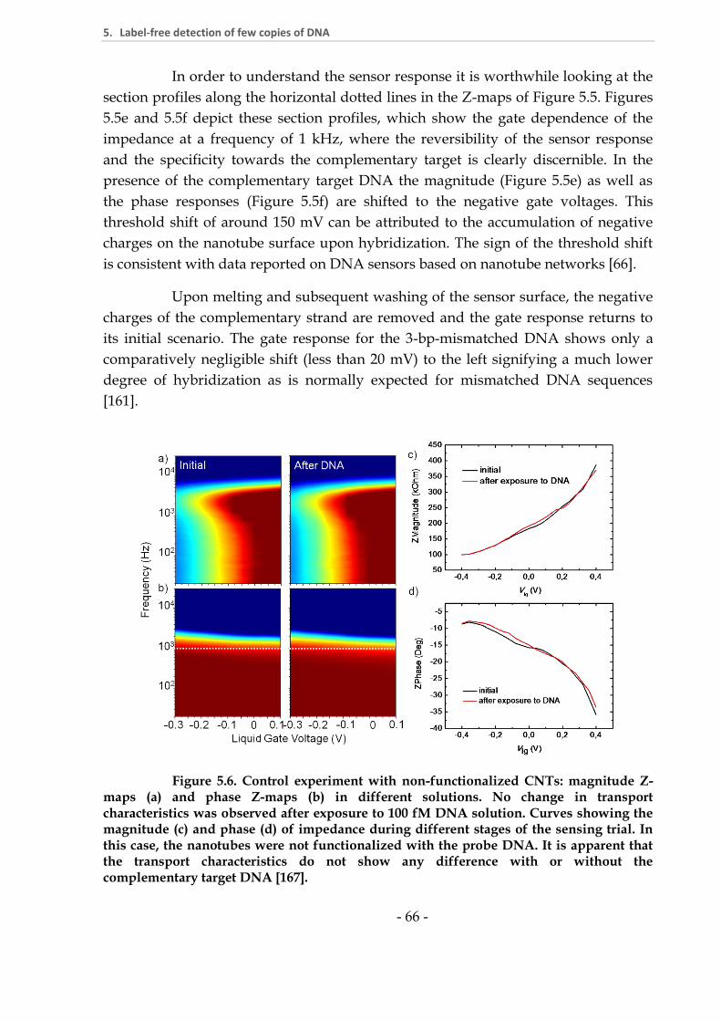
5. Label-free detection of few copies of DNA
- 66 -
In order to understand the sensor response it is worthwhile looking at the
section profiles along the horizontal dotted lines in the Z-maps of Figure 5.5. Figures
5.5e and 5.5f depict these section profiles, which show the gate dependence of the
impedance at a frequency of 1 kHz, where the reversibility of the sensor response
and the specificity towards the complementary target is clearly discernible. In the
presence of the complementary target DNA the magnitude (Figure 5.5e) as well as
the phase responses (Figure 5.5f) are shifted to the negative gate voltages. This
threshold shift of around 150 mV can be attributed to the accumulation of negative
charges on the nanotube surface upon hybridization. The sign of the threshold shift
is consistent with data reported on DNA sensors based on nanotube networks [66].
Upon melting and subsequent washing of the sensor surface, the negative
charges of the complementary strand are removed and the gate response returns to
its initial scenario. The gate response for the 3-bp-mismatched DNA shows only a
comparatively negligible shift (less than 20 mV) to the left signifying a much lower
degree of hybridization as is normally expected for mismatched DNA sequences
[161].
Figure 5.6. Control experiment with non-functionalized CNTs: magnitude Z-maps (a) and phase Z-maps (b) in different solutions. No change in transport characteristics was observed after exposure to 100 fM DNA solution. Curves showing the magnitude (c) and phase (d) of impedance during different stages of the sensing trial. In this case, the nanotubes were not functionalized with the probe DNA. It is apparent that the transport characteristics do not show any difference with or without the complementary target DNA [167].

5. Label-free detection of few copies of DNA
- 67 -
Nanotubes that were not functionalized with ABA with or without
subsequent coupling of probe DNA did not show any significant response towards
complementary sequence even at the highest concentration used here (Figure 5.6)
[167].
Figure 5.7. Attomolar detection limit of CNT-DNA-sensors. (a) Magnitude Z-map and (b) Phase Z-map for various concentrations of complementary target DNA. After every exposure of the sensor to target DNA, the hybrids were melted in order to obtain the initial state as shown in Figure 5.5 (a-c). It is apparent that even at a concentration of 100aM (corresponding to around 1800 molecules in our 30 µL droplet), the sensor response can be unambiguously discerned, signifying the ultrahigh sensitivity of CNT impedance biosensors [167].
5.6. Sensitivity and detection limit. The use of high
frequency detection ensures a very low noise of the electrical measurements. The
Ag/AgCl reference electrode provides for excellent stability. This enables the
repetitive use of the same sensor for a series of different DNA concentrations with
minimal drifts. Figure 5.7 collects the concentration dependence of the sensor
response for one of the devices, displaying the magnitude Z-maps (Figure 5.7a) and
phase Z-maps (Figure 5.7b) for the various concentrations of complementary target
DNA. Section profiles as extracted from the maps in Figure 5.7a are collected in
Figure 5.8a. It is apparent that the gate response shifts to increasing negative gate
voltages with increasing concentration of target DNA [167].

5. Label-free detection of few copies of DNA
- 68 -
Figure 5.8. Sensitivity of CNT-DNA-sensors: (a) Gate dependence of the magnitude of impedance at a frequency of 1 kHz in buffer (black line) and for varying concentrations of complementary target DNA in buffer (extracted from Figure 5.7a). The threshold voltage shifts to more negative voltages with increasing concentrations of DNA. (b) Calibration curve showing the threshold shift as a function of complementary (cDNA) and non-complementary (ncDNA) concentrations showing a linear response over a broad concentration range [167].
Figure 5.8b presents the calibration curve where the shift in threshold
voltage is plotted as a function of target DNA concentration. It is apparent that the
sensor response is linear over a broad concentration range and a concentration as low
as 100 aM can be unambiguously detected. The threshold voltage shift caused by
non-specific binding of non-complementary DNA (Figure 5.8b – blue line) is
significantly lower for all tested concentrations. This corresponds to around 1800
molecules of target DNA in our 30 µL sample droplet in the microwell. This is the
lowest detectable concentration that has been reported using any label-free or
mediator-free direct detection technique [167].

5. Label-free detection of few copies of DNA
- 69 -
5.7. Detection in complex media. In order to evaluate the
use of presented nanobiosensors in a realistic application scenario, we have validated
our analytical strategy towards the specificity of DNA differentiation at ultralow
concentrations. For this purpose, we have taken a heterogeneous mixture of three
different DNA sequences (ncDNA – noncomplementary to the probe sequence) each
at a concentration of 3 fM. To this we add 200 aM of complementary DNA (cDNA)
giving a total DNA concentration of 9.2 fM. The amount of cDNA we are aiming to
detect corresponds to just around 2% of the total DNA present in the solution
mixture. As a control we use the ncDNA mixture without the cDNA at the same total
DNA concentration. Figure 5.9 collects the Z-maps measured in various analyte
solutions [167].
Figure 5.9. Attomolar target differentiation in a heterogeneous DNA mixture. Magnitude Z-maps (a) in buffer (b) in buffer with a heterogeneous mixture of three different non-complementary sequences (ncDNA) each at 3 fM giving a total DNA concentration of 9 fM (denoted as 1) and (c) in solution 1 with added 200 aM of complementary target DNA (denoted as 2). (d) Sensor signal (threshold shift) for solutions 1 and 2. In 2, the complementary target amounts to just 2% of total DNA. The CNT-DNA-sensor is capable of differentiating this small amount from the high 9 fM non-complementary background, signifying a high selectivity coupled to an ultralow detection limit [167].

5. Label-free detection of few copies of DNA
- 70 -
It is apparent that the sensor response shifts clearly towards negative gate
voltages, similar to Figure 5.5. A significant shift is only seen if the buffer contained
the complementary target (Figure 5.9c). This is further clear from the threshold
voltage shift collected in Figure 5.9d for the heterogeneous sample with and without
the complementary DNA. It is apparent that 200 aM of target DNA comprising just
2% of the heterogeneous sample is able to bring in a significant threshold shift of
around 65mV. On the other hand, the 9fM ncDNA control solution without the
cDNA shows only a shift of around 12 mV, which is below the 20 mV occurring due
to non-specific interactions (as mentioned earlier – paragraph 5.5) [167].
5.8. Conclusions. The power of presented nanosensor is apparent
from the above described measurements and soars hopes of extending the technique
to directly detect low quantities of DNA from realistic biological samples such as
blood (after preprocessing), thereby showing promise for use in a clinical setting
without amplification or labeling steps. As mentioned earlier, the ability to detect
few copies of the DNA is made possible primarily by ensuring that the high surface-
to-volume ratio is guaranteed through appropriate passivation of the electrodes,
leaving exclusively the nanotube surface as the active element. Furthermore, the low
resistance, the stability gained by using the impedance measurement and the site-
specific electrochemical functionalization route have been crucial in achieving this
ultra-low detection limit.

6. Towards graphene-based electrical
sensors
6.1. Introduction. In spite of the constant efforts from the
researchers, the integration of graphene into devices still remains challenging.
Mechanical exfoliation of graphene from graphite crystal followed by e-beam
lithography is the commonly used technique for the preparation of contacted
graphene flakes [68, 180]. This approach is widely used in the research laboratories,
but has a number of limitations, for example, critical manual operation steps which
cannot be automated. Therefore this approach is unsuitable for device production at
the industrial level. Moreover the chips produced in this manner may have differing
geometry and position of contacts and flakes. This can complicate manufacturing and
operation of the devices at later stages. Researchers are trying to overcome these
limitations by using chemical vapor deposition (CVD) grown graphene as a starting
material for device fabrication [181-183].
Solution-based approaches for the preparation of carbon-based devices
offer the possibility for large-scale processing without using bulky equipment or
operation at very high-temperatures. Graphene suspension can be obtained from
graphite through intercalation using organic solvents, surfactants, etc [184]. Another
solution-based approach is to produce an aqueous solution of oxidized form of
graphene (Graphene oxide - GO) which is hydrophilic due to the presence of polar
groups, such as carboxyl, hydroxyl and epoxygroups [104, 185]. Graphene oxide is
insulating but it can be made conductive after a reduction process [103, 187]. The
resulting material is called reduced graphene oxide (RGO). To fabricate RGO devices
using this kind of suspension drop casting of the solution on the substrate with
subsequent contacting of the flakes of interest can be used. However this approach
does not improve the scalability of the fabrication. Therefore pre-patterning of the
surface and dielectrophoresis have been used to position the flakes at the desired
locations [186 - 190].

6. Towards graphene-based electrical sensors
- 72 -
6.2. DEP trapping of graphene. Several approaches for
solution based graphene devices fabrication were investigated here. Prior to the
fabrication of graphene devices using dielectrophoresis a solution of graphene or
graphene oxide must be prepared. Solutions containing graphene flakes were
obtained by 10 min sonication of graphite powder in dimethylformamide (DMF) and
Triton X-100. Large particles of graphite were removed using centrifugation (3000
rpm, 5 min). AFM imaging revealed the extreme inhomogeneity of resulting
suspensions. Dropcasting of the solution on a substrate and AFM measurements
showed the presence of large enough single or few-layer graphene flakes (Figure
6.1a). However, during the dielectrophoretic trapping (500kHz, 1V, 10 sec) which
was performed to position graphene from these solutions at the electrodes, along
with the single or few-layer graphene flakes, large graphite particles were trapped
(Figure 6.1 b). Further attempts to purify the solution led to a decrease of the
graphene flakes size, which complicated bridging of the gap between the electrodes
(Figure 6.1 c). Therefore other methods were considered as alternative solution-based
approaches for the fabrication of graphene-devices.
Figure 6.1. Liquid phase exfoliation of graphene from graphite. a - AFM
images of few-layer graphene flake obtained by exfoliation of graphite in DMF, b –
graphene flakes dielectrophoretically trapped together with large graphite particles, c –
individual graphene flakes trapped at electrodes using DEP.
6.3. DEP trapping of graphene oxide. As it was discussed
above, an alternative route was to prepare graphene oxide solution, followed by DEP
trapping and reduction. GO solution was prepared using Hummers method [191]. 1g
of graphite powder (200µm grain size) was added under constant stirring to the flask
with 23 ml of 98% sulfuric acid. 0.5 g of NaNO3 was added and the speed of stirring
was increased. After that 3 g of KMnO4 was added carefully. The above mentioned
procedures were performed in the ice bath with the temperature control of the

6. Towards graphene-based electrical sensors
- 73 -
solution. The temperature of the mixture was kept below 20oC. Upon removing the
iced water bath, the temperature was increased to 35oC in 30 minutes, leaving a grey
paste. 46 ml of deionized water was then added and the temperature was increased
to 98oC where it was maintained for 15 minutes. Then 70 ml of water was poured
into the mixture. 3% H2O2 was added slowly until the solution turned bright yellow.
The suspension was vacuum filtered resulting in a yellow brown filtrate which was
washed several times with water. The exfoliation was performed by overnight
shaking. The obtained graphite oxide suspension in water was centrifuged at 3000
rpm for 3 minutes to remove large particles.
Figure 6.2. Preparation of graphene oxide solution
Before DEP the GO solution was diluted 1:10 with water and sonicated for
5 seconds. DEP trapping was performed by applying 500 kHz, 10 V AC-voltage for
15 second. Afterwards the device was washed with water and isopropanol and blow-
dried in nitrogen flow. Then GO was thermally reduced in the furnace at 350oC for 1
hour in an inert atmosphere (argon). The devices prepared in this manner showed
resistances in the range of 200kOhm to 2 MOhm. Due to incomplete reduction the
resistance of the obtained devices is higher than in the case of pristine graphene but
the fabrication is rather simple and scalable. Another advantage of the GO-based
approach for fabrication of devices for biosensing is that the remaining oxygen
containing functionalities can be used for chemical functionalization of RGO.

6. Towards graphene-based electrical sensors
- 74 -
The RGO devices can be further improved for the use in liquids by
passivating the metal electrodes as it was done for CNT devices [130, 167]. An
example of device prepared in this manner is shown in Figure 6.3
Figure 6.3. An RGO device with passivated contacts for biosensing applications.
The devices were assembled on a chip-carrier for impedance
measurements in a liquid gated configuration. The reservoir for liquid was made
using PDMS plate as it was described previously (paragraph 5.2). Impedance
measurements were performed for the range of the gate voltages from -0.4 to 0.4 V.
Figure 6.4. shows the typical 2D-ZMagnitude–map of RGO device (a) and its gate
dependence at 1000 Hz (b) [130, 167].

6. Towards graphene-based electrical sensors
- 75 -
Figure 6.4. Liquid gating of RGO device. a) 2D-map of the magnitude of
impedance, b) gate dependence of the device at a fixed frequency of 1000 Hz.
6.4. Chemical anchoring of graphene oxide for
preparation of the devices. DEP of GO often results in the trapping of
several flakes. The devices prepared in this manner therefore are not as reproducible
as they are required to be. Moreover, the flakes often have numerous wrinkles and
folds. Therefore, an alternative chemical route for positioning GO flakes at the
desired location was proposed. It utilizes the presence of the various reactive
functional groups in graphene oxide [103]. These functional groups can be used as
hooks for anchoring the graphene flakes on the electrode surface previously
functionalized with appropriate reactive groups. Selective modification of the
electrodes can be achieved using electrochemical reactions. In this case, relevant
functional groups for coupling the functionalities on graphene oxide will be
selectively present on the surface of the electrodes [192].

6. Towards graphene-based electrical sensors
- 76 -
Figure 6.5. Scheme of the chemical anchoring protocol. (a) electrochemical functionalization of Pt electrodes with tyramine leading to (b) a coating of polytyramine on the electrode surface; (c) incubation of the chip in a GO solution results in the coupling of GO flakes to the polytyramine layer; (d) annealing in argon at 350oC leads to the removal of the polytyramine layer and the reduction of most of the oxygen containing groups. WE – working electrode, CE – counter electrode, RE – reference electrode [192].
The platinum electrodes were modified by oxidative polymerization of
tyramine with the formation of a thin film of polytyramine (pTy) which has a high
density of free aminogroups (Figure 6.5 a,b) [193]. Previously the immobilization of
biomolecules on microelectrodes with the help of electropolymerized tyramine was

6. Towards graphene-based electrical sensors
- 77 -
successfully demonstrated [194, 195]. Amine-containing polymers have been shown
to be effective for cross-linking of graphene oxide sheets via amino-epoxy coupling
[196]. The polymerization of tyramine was carried out by applying 0.8V for 15 sec at
the platinum electrodes pre-written on the silicon substrates which where immersed
into 10mM tyramine solution in 10mM H2SO4 using CompactStat potentiostat (Ivium
technologies). Platinum wires were used as counter and pseudo-reference electrodes.
After electrochemical deposition of polytyramine the substrate was washed with
ethanol and water and dried in nitrogen flow. For the coupling of pTy with graphene
oxide we immersed the substrate in a suspension of graphene oxide and left it for 1h
in a shaker. During the incubation of the sample in GO solution pTy reacts with
graphene oxide and acts as an anchor on the electrode surface (Figure 6.5c).
Afterwards, the substrate was taken out of the GO solution, immediately washed
with water and isopropanol and dried in nitrogen flow. After that the sample was
thermally annealed in inert atmosphere (argon) at 350oC for 1 hour (Figure 6.5d).
After cooling down to the room temperature the sample was washed with
isopropanol and dried [192].
Figure 6.6. Surface characterization by AFM. Inset - AFM image of a typical sample obtained at the end of the chemical anchoring protocol. The electrode gap and the immobilized graphene oxide flake are visible here. Main plot - Height profiles (along the red line in the AFM image) taken at a GO-free region on the electrode – as extracted from AFM images recorded at various stages of the anchoring procedure. It is apparent that the pTy film after electrodeposition is 5 to 8 nm thick (red curve). Annealing leads to the reduction in electrode height (blue curve) to the initial value signifying the removal of the pTy film [192].
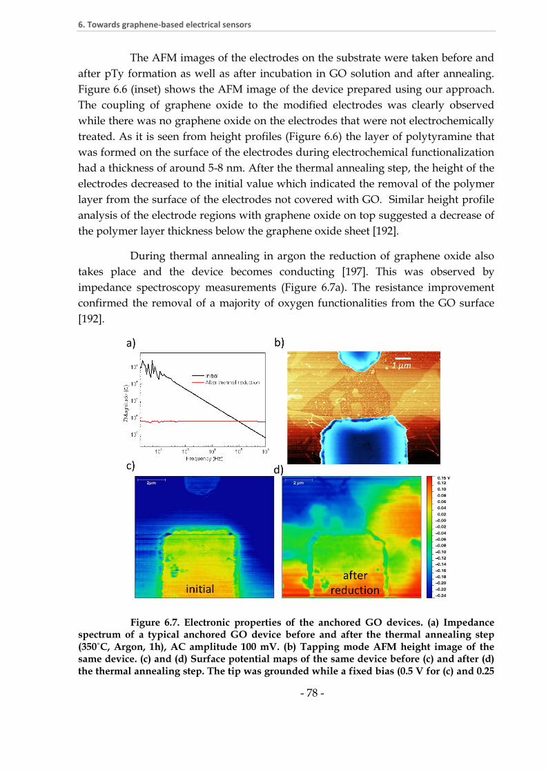
6. Towards graphene-based electrical sensors
- 78 -
The AFM images of the electrodes on the substrate were taken before and
after pTy formation as well as after incubation in GO solution and after annealing.
Figure 6.6 (inset) shows the AFM image of the device prepared using our approach.
The coupling of graphene oxide to the modified electrodes was clearly observed
while there was no graphene oxide on the electrodes that were not electrochemically
treated. As it is seen from height profiles (Figure 6.6) the layer of polytyramine that
was formed on the surface of the electrodes during electrochemical functionalization
had a thickness of around 5-8 nm. After the thermal annealing step, the height of the
electrodes decreased to the initial value which indicated the removal of the polymer
layer from the surface of the electrodes not covered with GO. Similar height profile
analysis of the electrode regions with graphene oxide on top suggested a decrease of
the polymer layer thickness below the graphene oxide sheet [192].
During thermal annealing in argon the reduction of graphene oxide also
takes place and the device becomes conducting [197]. This was observed by
impedance spectroscopy measurements (Figure 6.7a). The resistance improvement
confirmed the removal of a majority of oxygen functionalities from the GO surface
[192].
Figure 6.7. Electronic properties of the anchored GO devices. (a) Impedance spectrum of a typical anchored GO device before and after the thermal annealing step (350˚C, Argon, 1h), AC amplitude 100 mV. (b) Tapping mode AFM height image of the same device. (c) and (d) Surface potential maps of the same device before (c) and after (d) the thermal annealing step. The tip was grounded while a fixed bias (0.5 V for (c) and 0.25

6. Towards graphene-based electrical sensors
- 79 -
V for (d) was applied across the gap. It can be inferred that the annealing step improves the resistance and the electronic properties of the anchored flakes [192].
In order to gather further support for the improvement in transport upon
annealing, the devices were investigated using Kelvin Probe Force Microscopy [198,
199]. The resulting surface potential maps are depicted in Figures 6.7c and 6.7d. In
the former case, there is no conducting pathway measurable in the device before
annealing, consistent with its insulating behavior. By contrast, after annealing the
current carrying flake can be clearly identified in Figure 6.7d, analogous to recent
results on individually contacted RGO flakes [200]. This leads us to conclude that the
annealing procedure serves as a single processing step that results in a graphene-like
backbone of the GO flakes, while simultaneously removing the polytyramine layer at
the contacts [192].
6.5. Up-scaling the fabrication of RGO devices. The
advantage of the offered approach for device fabrication is the possibility to scale-up
the process. Towards this goal, we utilized a specialized layout as shown in Figure
6.8a. The substrates comprised of 6 mm x 30 mm Si/SiO2 chips allowing for long
leads. The long leads enable us to perform electronic transport measurements in
liquids as is discussed later. Each chip comprises of 6 electrode gaps. All the 12
electrodes are initially wire-bonded in the outer region of the substrate to form a
parallel connection of 12 electrodes. In this manner all the electrodes can be
decorated electrochemically with polytyramine in a single step. A drop of tyramine
solution was placed in the region of the gaps. Pt wires used as counter and reference
electrodes were inserted into this drop. The voltage applied to one of the pads of
connected electrodes led to an electrochemical reaction on all of them at the same
time. Placing such a sample into the GO solution led to the coupling of graphene
oxide to all of the electrodes on the surface. The contacts of the devices were
passivated using an appropriate mask and a mask aligner MA-6 (SüssMicrotech).
The resulting passivated devices are shown in Figure 6.8b. Liquid gate dependence
was measured in water using Ag/AgCl reference electrode to apply the gate voltage
and PDMS plate with the hole to form a well. The contacts to the electrodes were
located outside PDMS well. The devices showed resistances in a range of 100kOhm –
1 MOhm which is comparable to the reduced graphene oxide devices obtained by
dielectrophoretic trapping of GO followed by reduction. Liquid gate dependence of a
typical device is shown in Figure 6.8c [192].

6. Towards graphene-based electrical sensors
- 80 -
Figure 6.8. Scaling up chemical anchoring. (a) Device layout showing 6 electrode gaps. Initially, the 12 electrodes are linked externally through wire bonding. For liquid gating measurements, a liquid channel connected by two circular wells is created with the help of a polydimethylsiloxane (PDMS) layer. The inset shows a close-up of the electrode gap and the relative extent of the liquid channel. An Ag/AgCl reference electrode inserted in the channel serves as the gate electrode. (b) AFM images of the 6 gap positions (from one chip) at the end of the chemical anchoring protocol. In addition to the steps shown in Figure 6.5, the electrodes are passivated with SiO2 using a separate photo mask. (c) Liquid gate dependence of resistance of one of the RGO devices, showing the typical ambipolar behavior [192].
From the foregoing discussions it is apparent that the chemical anchoring
protocol serves as a versatile route to obtain RGO field-effect devices with a high
throughput. The real advantage of such a technique in an industrial scenario requires
the demonstration of such a protocol at the wafer scale. Furthermore, the feasibility
of this protocol for other substrates, such as glass or polymers, is also an important
factor. To evaluate this, we have fabricated electrodes on 4” glass wafers using
photolithography as shown in Figure 6.9a. The wafer is segmented into chips, each of
which is laid out as shown in Figure 6.8a. The layout is designed in such a way that
the electrodes of the chips in the region marked with the red dashed line (Figure

6. Towards graphene-based electrical sensors
- 81 -
6.9a) are all connected to each other through the large common pads. After carrying
out the chemical anchoring protocol, the wafer is diced whereby these electrode
connections are lost resulting in standalone chips with 6 individual gaps each. For
the wafer in Figure 6.9a, 77 working devices (out of 90 electrode gaps) were obtained
signifying a yield of 86%. A histogram of the resistances from these 77 devices is
presented in Figure 6.9 b, with resistances in the range of 200 kOhm to 3 MOhm
[192].
Figure 6.9. Wafer scale RGO devices with high yield. (a) A photograph of a 4” glass wafer with photolithographically patterned electrodes. The electrodes in the red dashed region are connected to each other through the large pads in the upper left and lower bottom. These large pads are used to deposit a polytyramine layer on all the electrodes in a single step. There are 15 chips in red dashed region, each chip containing six electrode gaps with an electrode layout as shown in Figure 6.8a. (b) Histogram of resistances of 77 out of the 90 electrode gaps at the end of the chemical anchoring protocol. 13 devices showed very high resistances [192].
These results underline the scalability of this approach demonstrating a
capability to obtain RGO devices at a high yield. The devices prepared on wafers
showed higher resistances on the average in comparison to those observed on
individual samples. This could be improved by optimizing the conditions of
electropolymerization and thermal reduction for the substrate of interest.
It is worth mentioning here that this approach was also successfully
implemented on substrates with differing electrode geometries, as well as on flexible
kapton foils (Figure 6.10).
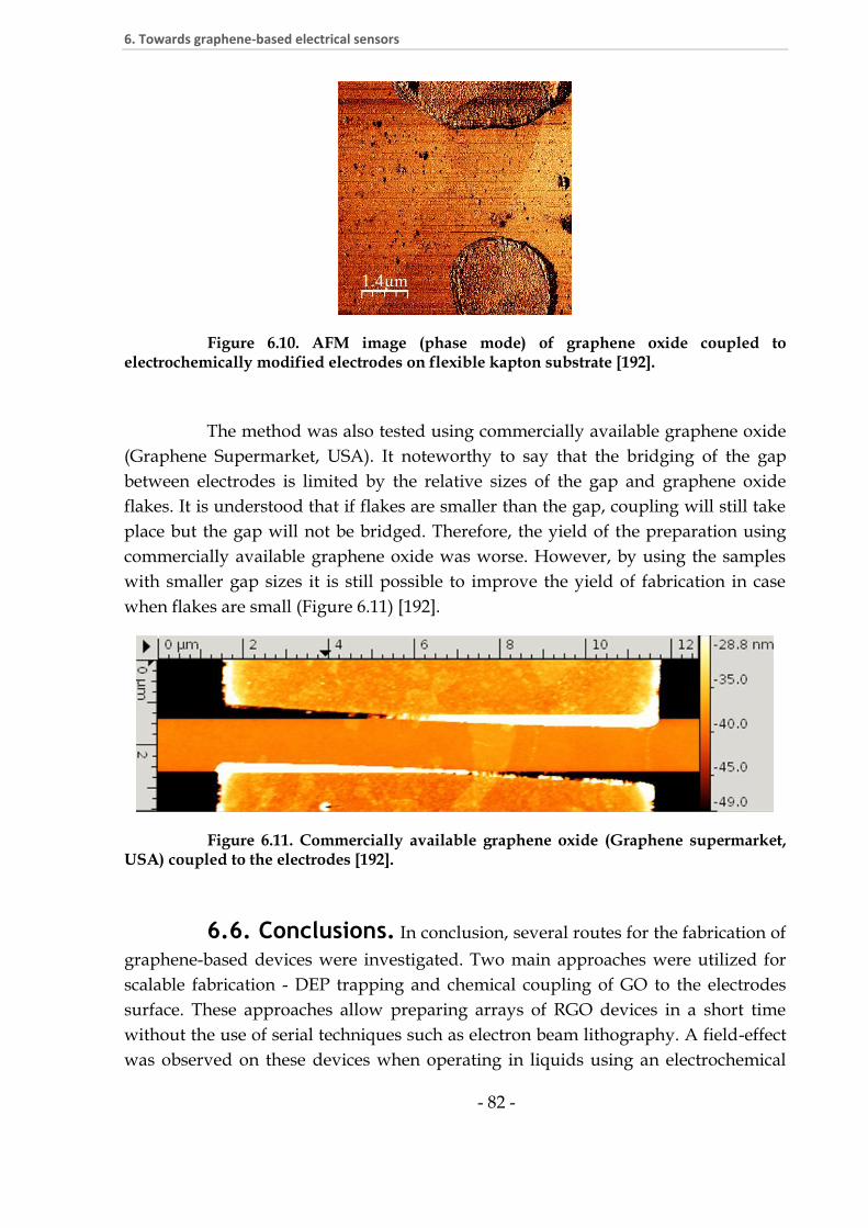
6. Towards graphene-based electrical sensors
- 82 -
Figure 6.10. AFM image (phase mode) of graphene oxide coupled to electrochemically modified electrodes on flexible kapton substrate [192].
The method was also tested using commercially available graphene oxide
(Graphene Supermarket, USA). It noteworthy to say that the bridging of the gap
between electrodes is limited by the relative sizes of the gap and graphene oxide
flakes. It is understood that if flakes are smaller than the gap, coupling will still take
place but the gap will not be bridged. Therefore, the yield of the preparation using
commercially available graphene oxide was worse. However, by using the samples
with smaller gap sizes it is still possible to improve the yield of fabrication in case
when flakes are small (Figure 6.11) [192].
Figure 6.11. Commercially available graphene oxide (Graphene supermarket, USA) coupled to the electrodes [192].
6.6. Conclusions. In conclusion, several routes for the fabrication of
graphene-based devices were investigated. Two main approaches were utilized for
scalable fabrication - DEP trapping and chemical coupling of GO to the electrodes
surface. These approaches allow preparing arrays of RGO devices in a short time
without the use of serial techniques such as electron beam lithography. A field-effect
was observed on these devices when operating in liquids using an electrochemical

6. Towards graphene-based electrical sensors
- 83 -
gate. This is important for the electrical biosensing applications. The ability to realize
wafer-scale RGO devices on arbitrary substrates is an important step towards their
widespread use in a number of fields [192].

Summary and outlook
7.1. CNT based electrical sensors. In this thesis the electrical
biosensing platforms based on electrochemically functionalized carbon nanotubes
are presented. The important aspect of this work was the optimization of the sensor
fabrication procedure. The device fabrication steps were optimized to ensure high
throughput of this process. Thus, Si/SiO2 samples with photolitographically written
Pt electrodes were used as substrates for the fabrication of nanosensors. The scalable
assembly of CNTs into devices was achieved by dielectrophoretic trapping of the
nanotubes from their dispersion. This ensures low-cost, reproducibility and
possibility of automation of the CNT sensor fabrication. Sensitivity and robustness of
the sensors was improved considerably with the help of passivation of the metal
contacts with insulating layer. Electrochemical functionalization strategy, used in this
work, provided site-specific modification of the nanotubes. Site-specificity of
functionalization is one of the crucial requirements for achieving high sensitivity of
the sensor. It also makes it possible to fabricate on the same chip several nanosensors
designed to detect different analytes. Multiplex detection of several analytes can be
realized in this manner. This will pave way for lab-on-a-chip systems that can be
tailored for specific applications in point-of-care diagnostics.
In this work biosensing is based on the measurement of the impedance of the
modified CNTs at different liquid-gate voltages. Impedance measurements in field-
effect configuration of the device ensure low signal to noise. Glucose detection with
boronic acid functionalized CNT devices helped to reveal mechanisms of sensing
using the presented biosensing configuration. Finally, very high sensitivity and
selectivity of the designed nanosensors were achieved in the case of DNA detection.
Nevertheless, demonstrated sensing platform leaves a lot of room for further
development and improvement.
For example, in the case of DNA sensing, the experiments were conducted
with synthetic oligonucleotides. It will be important to demonstrate this high
sensitivity with real nucleic acid sequences obtained from biological samples.
Possible analytes for such tests can be microRNA (miRNA) molecules. MicroRNAs
are small (18 to 25 nucleotides) regulatory genes [201]. They can inhibit the

7. Summary and outlook
- 85 -
expression of target protein-coding gene. The suppression of the protein expression
occurs due to the complementarity of the miRNA to a part of one or more messenger
RNAs [202]. This inhibits translation of the protein. It was discovered that miRNAs
circulate in blood serum. The concentration of some of the circulating miRNA
changes depending on the pathological states of the organism, like sepsis,
autoimmune diseases, cardiac diseases and cancer [203-207]. Taking into account the
stability of miRNA they can serve as potential biomarkers of various diseases [204,
208, 209]. The low concentration of miRNAs in serum requires highly sensitive and
selective methods for their quantification. The biosensing platform described in this
thesis may potentially be applied for this purpose.
Figure 7.1. Sensing of let-7a-miRNA in buffer (a) and serum (b).
Towards this goal the first miRNA sensing trials were conducted. We used let-
7a-miRNA as an analyte and a DNA sequence complementary to it as a receptor. The
fabrication of the sensor, functionalization of CNTs and electrical detection were
performed in the same way as in the case of the DNA sensor. The results obtained
during the sensing of let-7a-miRNA in buffer were similar to that of DNA detection
(Figure 7.1 a). The gate characteristic shifts to the left after the CNT-device was
exposed to a 100 fM let-7a solution.
However, the detection of miRNA in serum was not straightforward. miRNA
added to serum diluted with working buffer (1:10) did not cause significant changes
in the gate dependence of the sensor (Figure 7.1 b). This can be explained by the
presence of the proteins and metabolites in serum which may affect the access of the
target RNA to the carbon nanotube. The AFM images of the device taken after
sensing trials in serum showed the contamination of SiO2 and CNT surface (Figure
7.2). It is clear that the sensing protocol should be optimized for the direct
measurement of analytes from the serum. One possibility to improve this is to

7. Summary and outlook
- 86 -
perform a pretreatment of the serum samples, like liquid-liquid or solid-phase
extraction, protein precipitation, etc [210].
Figure 7.2. AFM images of the device before (a) and after (b) sensing trials in serum.
7.2. Graphene devices for biosensing. Although CNT-
sensors show good sensitivity, their reproducibility suffers from the inhomogeneity
of the starting material. Therefore, graphene was considered as an alternative
nanomaterial to be used as transducing element of the nanosensors. Several
approaches for large-scale fabrication of the graphene or reduced graphene oxide
were tested here. The graphene oxide solution was used for the wafer scale
fabrication of RGO devices using a novel chemical approach. This fabrication
protocol is suitable for building FET-based sensors. With such sensors it is possible to
utilize the same detection strategy as it was used here for CNT-FET-sensors (Figure
7.3).
Figure 7.3. Schematic of RGO-FET- immunosensor.

7. Summary and outlook
- 87 -
Preliminary results on the detection of amyloid-beta peptide were obtained
with the RGO-devices. Amyloid beta peptide is an important marker for the
diagnostics of Alzheimer disease [211]. In order to detect amyloid-beta, RGO was
modified with a specific monoclonal antibody. Z-Maps were obtained for gate
voltages from -0.4 V to 0.4 V on the devices before and after their exposure to the
solution of target peptide.
Figure 7.4. Sensing of beta-amyloid peptide using RGO immunosensor. Z-Maps of the magnitude of impedance before (a) and after (b) exposure to 50pM beta-amyloid solution (scale - 2kOhm to 2.5 MOhm). c) gate characteristics of the device at 100 Hz.

7. Summary and outlook
- 88 -
A clear shift of the gate-dependence curves was observed after the amyloid
beta solution was introduced (Figure 7.4). This shift can be explained by the
accumulation of amyloid beta on the RGO surface. Amyloid-beta peptide (pI 5.5)
carries a negative charge at a working pH of 7.4. This can cause a shift in the gate
dependence. The response was not completely reversible. After 90 minutes of wash
with high ionic strength buffer, the gate-dependence of the device comes back but
not exactly to the same level. This can be explained by a strong antigen-antibody
interaction. Future steps in this work will include the optimization of the sensing
protocol and the required control experiments.
Demonstrated carbon nanostructure-based sensing platforms show promise
for their application due to high sensitivity and low cost. It can be also optimized for
performing fundamental single-molecule and kinetic studies, which may benefit
from the high sensitivity of the measurements. Both CNT and graphene devices can
be used for the detection of low amounts of many other analytes relevant for the
medical diagnostics, food and environmental monitoring.

Bibliography
1. Atkinson AJ, Colburn WA, DeGruttola VG, Demets DL, Downing GJ, et al.
Biomarkers and surrogate endpoints: preferred definitions and conceptual
framework. Clin Pharmacol Ther. 2001, 69, 89–95.
2. Elin RJ. Instrumentation in clinical chemistry. Science. 1980, 210, 286–289.
3. Durner J. Clinical Chemistry: Challenges for Analytical Chemistry and the
Nanosciences from Medicine. Angew Chem Intern Ed. 2010, 49, 1026–105.
4. Kiechle FL, Holland CA. Point-of-care testing and molecular diagnostics:
miniaturization required. Clin Lab Med. 2009, 29, 555-560.
5. Holland CA, Kiechle FL. Point-of-care molecular diagnostic systems--past,
present and future. Curr Opin Microbiol. 2005, 85, 504-509.
6. Rasooly A. Moving biosensors to point-of-care cancer diagnostics. Biosensors &
Bioelectronics. 2006, 21, 1847-1850.
7. Lien K-Y, Lee G-B. Miniaturization of molecular biological techniques for gene
assays. Analyst. 2010, 135, 1499-1518
8. Mascini M, Tombelli S. Biosensors for biomarkers in medical diagnostics.
Biomarkers. 2008, 13, 637-657
9. Marks RS, Lowe CR, Cullen DC, Weetall HH, Karube Isao. Handbook of
Biosensors and Biochips. 2007, Wiley, DOI: 10.1002/9780470061565
10. Clark LC, Lyons C. Electrode systems for continuous monitoring in
cardiovascular surgery. In: Ann. N.Y. Acad. Sci. Bd, 1962, 102, 3129–3145
11. Rechnitz GA, Kobosa RK, Riechela SJ, Gebauer CR. A bio-selective membrane
electrode prepared with living bacterial cells. Analytica Chimica Acta. 1977, 94,
357-365
12. Chambers JP, Arulanandam BP, Matta LL, Weis W, Valdes JJ. Biosensor
Recognition Elements. Curr. Issues Mol. Biol. 10, 1–12.
13. Collings AF and Caruso F. Biosensors: recent advances. Rep. Prog. Phys. 1997,
60, 1397–1445.
14. Joseph D. Bronzino. Medical devices and systems. CRC Press, 2006
15. North SH, Lock EH, Taitt CR, Walton SG. Critical aspects of biointerface
design and their impact on biosensor development. Anal Bioanal Chem. 2010,
397, 925-933.
16. Azzazy HME, Mansour MMH, Kazmierczak SC. Nanodiagnostics: A New
Frontier for Clinical Laboratory Medicine. Clinical Chemistry. 2006, 52, 1238–
1246.

- 90 -
Bibliography
17. Roy S and Gao Z. Nanostructure-based electrical biosensors. Nano Today. 2009,
4, 318-324.
18. Balasubramanian K. Challenges in the use of 1D nanostructures for on-chip
biosensing and diagnostics. Biosens. Bioelectron. 2010, 26, 1195-1204.
19. Rosi NL and Mirkin CA. Nanostructures in Biodiagnostics. Chem. Rev. 2005,
105, 1547-1562.
20. Erickson D, Mandal S, Yang AHJ and Cordovez B. Nanobiosensors:
optofluidic, electrical and mechanical approaches to biomolecular detection at
the nanoscale. Microfluid. Nanofluid. 2008, 4, 33-52.
21. Maroto A, Balasubramanian K, Burghard M and Kern K. Functionalized
metallic carbon nanotube devices for pH sensing. ChemPhysChem, 2007, 8, 220-
223.
22. Homola J. Surface Plasmon Resonance Based Sensors. 2006, Springer.
23. Ozkan M. Quantum dots and other nanoparticles: What they can offer to drug
discovery? Drug Discov. Today. 2004, 9, 1065-1071
24. Costa-Fernandez JM, Pereiro R and Medel SA. The use of luminescent
quantum dots for optical sensing. Tr. Anal. Chem. 2006, 25, 207-218.
25. Xu K, Huang JR, Ye ZZ, Ying YB and Li YB. Recent Development of Nano-
Materials Used in DNA Biosensors. Sensors. 2009, 9, 5534-5557.
26. Hu C and Hu S. Carbon Nanotube-Based Electrochemical Sensors: Principles
and Applications in Biomedical Systems. J. Sens. 2009, 187615-187645.
27. Vaddiraju S, Tomazos I, Burgess DJ, Jain FC and Papadimitrakopoulos F.
Emerging synergy between nanotechnology and implantable biosensors.
Biosens. Bioelectron. 2010, 25, 1553-1565.
28. Yogeswaran U and Chen SM. A Review on the Electrochemical Sensors and
Biosensors Composed of Nanowires as Sensing Material. Sensors, 2008, 8, 290-
313.
29. Siqueira JR, Caseli L, Cresphilo FN, Zucolotto V and Oliviera ON.
Immobilization of biomolecules on nanostructured films for biosensing.
Biosens. Bioelectron. 2010, 25, 1254-1263.
30. Kurkina T, Balasubramanian K. Towards in vitro molecular diagnostics using
nanostructures. Cell Mol Life Sci. 2012, 69, 373-88
31. Fiorini GS, Chiu DT. Disposable microfluidic devices: fabrication, function,
and application. Biotechniques. 2005, 38, 429-446.
32. Haeberle S, Zengerle R. Microfluidic platforms for lab-on-a-chip applications.
Lab Chip. 2007, 7, 1094-110.
33. Rivet C, Lee H, Hirsch A, Hamilton S, Lu H. Microfluidics for medical
diagnostics and biosensors. Chemical EngineeringScience. 2011, 66, 1490–1507.
34. Wang J. Electrochemical biosensors: Towards point-of-care next term cancer
diagnostics. Biosens Bioelectron. 2006, 21, 1887-92.
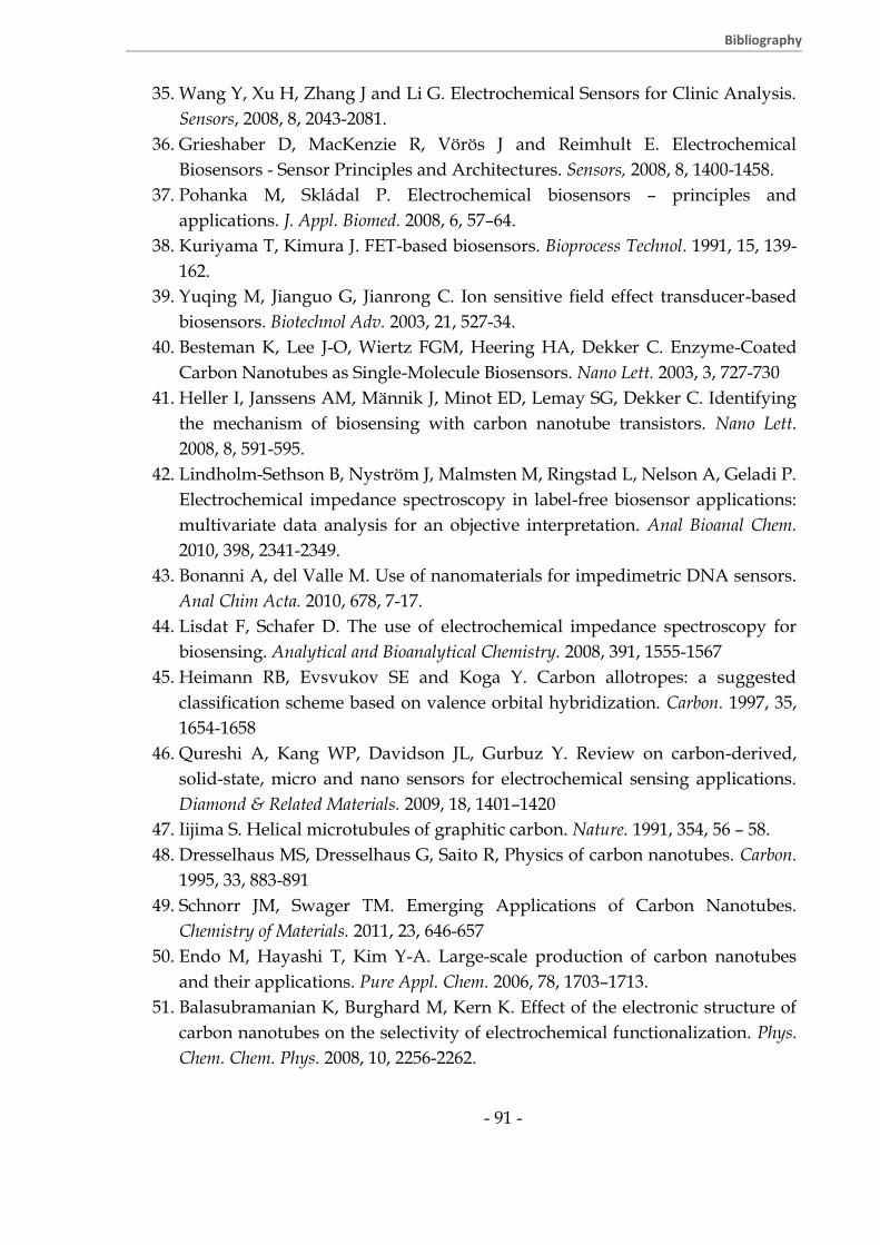
- 91 -
Bibliography
35. Wang Y, Xu H, Zhang J and Li G. Electrochemical Sensors for Clinic Analysis.
Sensors, 2008, 8, 2043-2081.
36. Grieshaber D, MacKenzie R, Vörös J and Reimhult E. Electrochemical
Biosensors - Sensor Principles and Architectures. Sensors, 2008, 8, 1400-1458.
37. Pohanka M, Skládal P. Electrochemical biosensors – principles and
applications. J. Appl. Biomed. 2008, 6, 57–64.
38. Kuriyama T, Kimura J. FET-based biosensors. Bioprocess Technol. 1991, 15, 139-
162.
39. Yuqing M, Jianguo G, Jianrong C. Ion sensitive field effect transducer-based
biosensors. Biotechnol Adv. 2003, 21, 527-34.
40. Besteman K, Lee J-O, Wiertz FGM, Heering HA, Dekker C. Enzyme-Coated
Carbon Nanotubes as Single-Molecule Biosensors. Nano Lett. 2003, 3, 727-730
41. Heller I, Janssens AM, Männik J, Minot ED, Lemay SG, Dekker C. Identifying
the mechanism of biosensing with carbon nanotube transistors. Nano Lett.
2008, 8, 591-595.
42. Lindholm-Sethson B, Nyström J, Malmsten M, Ringstad L, Nelson A, Geladi P.
Electrochemical impedance spectroscopy in label-free biosensor applications:
multivariate data analysis for an objective interpretation. Anal Bioanal Chem.
2010, 398, 2341-2349.
43. Bonanni A, del Valle M. Use of nanomaterials for impedimetric DNA sensors.
Anal Chim Acta. 2010, 678, 7-17.
44. Lisdat F, Schafer D. The use of electrochemical impedance spectroscopy for
biosensing. Analytical and Bioanalytical Chemistry. 2008, 391, 1555-1567
45. Heimann RB, Evsvukov SE and Koga Y. Carbon allotropes: a suggested
classification scheme based on valence orbital hybridization. Carbon. 1997, 35,
1654-1658
46. Qureshi A, Kang WP, Davidson JL, Gurbuz Y. Review on carbon-derived,
solid-state, micro and nano sensors for electrochemical sensing applications.
Diamond & Related Materials. 2009, 18, 1401–1420
47. Iijima S. Helical microtubules of graphitic carbon. Nature. 1991, 354, 56 – 58.
48. Dresselhaus MS, Dresselhaus G, Saito R, Physics of carbon nanotubes. Carbon.
1995, 33, 883-891
49. Schnorr JM, Swager TM. Emerging Applications of Carbon Nanotubes.
Chemistry of Materials. 2011, 23, 646-657
50. Endo M, Hayashi T, Kim Y-A. Large-scale production of carbon nanotubes
and their applications. Pure Appl. Chem. 2006, 78, 1703–1713.
51. Balasubramanian K, Burghard M, Kern K. Effect of the electronic structure of
carbon nanotubes on the selectivity of electrochemical functionalization. Phys.
Chem. Chem. Phys. 2008, 10, 2256-2262.

- 92 -
Bibliography
52. Hiura H, Ebbesen T W, Tanigaki K. Opening and purification of carbon
nanotubes in high yields. Advanced Materials. 1995, 7, 275-276.
53. Treacy MMJ, Ebbesen TW and Gibson JM. Exceptionally high Young's
modulus observed for individual carbon nanotubes. Nature, 1996, 381, 678-680.
54. Desprès JF, Daguerre E, Lafdi K. Flexibility of graphene layers in carbon
nanotubes. Carbon. 1995, 33, 87-92.
55. Ajayan PM, Stephan O, Colliex C, Trauth D. Aligned Carbon Nanotube
Arrays Formed by Cutting a Polymer Resin-Nanotube Composite. Science,
1994, 265, 1212-1214.
56. Sinha N, Ma J, Yeow JTW. Carbon Nanotube-Based Sensors. Journal of
Nanoscience and Nanotechnology. 2006, 6, 573–590
57. Chen Z, Tabakman SM, Goodwin AP, Kattah MG, Daranciang D, Wang X,
Zhang G, Li X, Liu Z, Utz PJ, Jiang K, Fan S and Dai H Protein microarrays
with carbon nanotubes as multicolor Raman labels. Nat. Biotechnol. 2008, 26,
1285-1292.
58. Yu X, Munge B, Patel V, Jensen G, Bhirde A, Gong JD, Kim SN, Gillespie J,
Gutkind JS, Papadimtrakopoulos F and Rusling JF. Carbon nanotube
amplification strategies for highly sensitive immunodetection of cancer
biomarkers. J. Am. Chem. Soc. 2006, 128, 11199-11205.
59. Balasubramanian K and Burghard M. Biosensors based on carbon nanotubes.
Anal. Bioanal. Chem. 2006, 385, 452-468.
60. Gruner G. Carbon nanotube transistors for biosensing applications. Anal.
Bioanal. Chem. 2006, 384, 322-335.
61. Sotiropoulou S, Chaniotakis NA, Carbon nanotube array-based biosensor.
Anal Bioanal. Chem. 2003, 375, 103-105.
62. Collins PG, Bradley K, Ishigami M, Zettl A. Extreme oxygen sensitivity of
electronic properties of carbon nanotubes. Science. 2000, 287, 1801-1804
63. Kong J, Franklin NR, Zhou C, Chapline MG, Peng S, Cho K, Dai H. Nanotube
molecular wires as chemical sensors. Science. 2000, 287, 622-625
64. Star A, Han T-R, Gabriel J-CP, Bradley K, Grüner G. Interaction of aromatic
compounds with carbon nanotubes. Nano Lett. 2003, 3, 1421-1423
65. Bradley K, Gabriel J-CP, Briman M, Star A, Grüner G. Charge transfer from
aqueous ammonia absorbed on nanotube transistors. Phys. Rev. Lett. 2003, 91,
2183011–2183014.
66. Star A, Tu E, Niemann J, Gabriel J-CP, Joiner C.S, Valcke C. Label-free
detection of DNA hybridization using carbon nanotube network field-effect
transistors. Proc. Natl. Acad. Sci.USA. 2006, 103, 921–926.
67. Maehashi K, Matsumoto K, Takamura Y, Tamiya E. Aptamer-based label-free
immunosensors using carbon nanotube field-effect transistors. Electroanalysis.
2009, 21, 1285-1290.

- 93 -
Bibliography
68. Novoselov KS, Geim AK, Morozov SV, Jiang D, Zhang Y, Dubonos SV,
Grigorieva IV and Firsov AA. Electric Field Effect in Atomically Thin Carbon
Films. Science. 2004, 306, 666-669
69. Sakhaee-Pour A, Ahmadian MT, Vafai A, Applications of single-layered
graphene sheets as mass sensors and atomistic dust detectors. Solid State
Communications. 2008, 145, 168-172.
70. Stoller MD, Park S, Zhu Y, An J and Ruoff RS. Graphene-Based
Ultracapacitors. Nano Lett, 2008, 8, 3498–3502
71. Sundaram RS, Gomez-Navarro C, Balasubramanian K, Burghard M, Kern K.
Electrochemical Modification of Graphene. Advanced Materials. 2008, 20, 3050–
3053.
72. Choi SH, Kim YL, Byun KM. Graphene-on-silver substrates for sensitive
surface plasmon resonance imaging biosensors. Opt Express. 2011, 19, 458-466
73. Peigney A, Laurent Ch, Flahaut E, Bacsa RR, Rousset A. Specific surface area
of carbon nanotubes and bundles of carbon nanotubes. Carbon. 2001, 39, 507-
514
74. Dong H, Gao W, Yan F, Ji H, Ju H. Fluorescence resonance energy transfer
between quantum dots and graphene oxide for sensing biomolecules. Anal.
Chem. 2010, 82, 5511–5517.
75. Lu C-H, Yang H-H, Zhu C-L, Chen X, Chen GN. A graphene platform for
sensing biomolecules. Angew. Chem. Int. Ed. 2009, 48, 4785–4787.
76. He S. et al. A graphene nanoprobe for rapid, sensitive, and multicolor
fluorescent DNA analysis. Adv. Funct. Mater. 2010, 20, 453–459.
77. Kang X, Wang J, Wu H, Aksay IA, Liu J and Lin Y. Glucose Oxidase–
graphene–chitosan modified electrode for direct electrochemistry and glucose
sensing Biosens.Bioelectron. 2009, 25, 901-905.
78. Liu Y, Yu D, Zeng C, Miao Z and Dai L. Biocompatible Graphene Oxide-Based
Glucose Biosensors. Langmuir, 2010, 26, 6158-6160.
79. Zhuang Z, Li J, Xu R, Dan X. Electrochemical Detection of Dopamine in the
Presence of Ascorbic Acid Using Overoxidized Polypyrrole/Graphene
Modified Electrodes. J. Electrochem. Sci. 2011, 6, 2149 – 2161.
80. Du D, Zou Z, Shin Y, Wang J, Wu H, Engelhard MH, Liu J, Aksay IA, Lin Y.
Sensitive Immunosensor for Cancer Biomarker Based on Dual Signal
Amplification Strategy of Graphene Sheets and Multienzyme Functionalized
Carbon Nanospheres. Anal. Chem. 2010, 82, 2989-2995.
81. Shao Y, Wang J, Wu H, Liu J, Aksay IA, Lina Y. Graphene Based
Electrochemical Sensors and Biosensors. Electroanalysis 2010, 22, 1027 – 1036.
82. Dan P, Lu Y, Kybert NJ, Luo ZT, Johnson ATC. Intrinsic Response of
Graphene Vapor Sensors. Nano Letters. 2009, 9, 1472-1475.

- 94 -
Bibliography
83. Schedin F, Geim AK, Morozov SV, Hill EW, Blake P, Katsnelson MI,
Novoselov KS. Detection of individual gas molecules adsorbed on graphene.
Nature Materials. 2007, 6, 652 – 655.
84. Ang PK, Chen W, Wee ATS, Loh KP. Solution-gated epitaxial graphene as pH
sensor. J. Am. Chem. Soc. 2008, 130, 14392–14393.
85. Dong X, Shi Y, Huang W, Chen P, Li LP. Electrical Detection of DNA
Hybridization with Single-Base Specificity Using Transistors Based on CVD-
Grown Graphene Sheets. Adv. Mater. 2010, 22, 1–5.
86. Mohanty N, Berry V. Graphene-based single-bacterium resolution biodevice
and DNA transistor: interfacing graphene derivatives with nanoscale and
microscale biocomponents. Nano Letters. 2008, 8, 4469–4476.
87. Ohno Y, Maehashi K, Yamashiro Y, Matsumoto K. Electrolyte-gated graphene
field-effect transistors for detecting pH and protein adsorption. Nano Letters.
2009, 9, 3318–3322.
88. Yang W, Ratinac KR, Ringer SP, Thordarson P, Gooding JJ, Braet F. Carbon
Nanomaterials in Biosensors: Should You Use Nanotubes or Graphene?
Angew. Chem. Int. Ed. 2010, 49, 2114 – 2138
89. Wang Y, Li Z, Wang J, Li J, Lin Y. Graphene and graphene oxide:
biofunctionalization and applications in biotechnology. Trends in
Biotechnology. 2011, 29, 205-212
90. Hirsch A, Vostrowsky O. Functionalization of Carbon Nanotubes. Topics in
Current Chemistry. 2005, 45, 193-237
91. Martinez MT, Tseng YC, Ormategui N, Loinaz I, Eritja R, Bokor J. Label-Free
DNA Biosensors Based on Functionalized Carbon Nanotube Field Effect
Transistors. Nano Letters. 2009, 9, 530–536
92. Geim AK. Graphene: Status and Prospects. Science. 2009, 324, 1530-1534
93. Loh KP, Bao Q, Ang PK, Yang . The chemistry of graphene. J. Mater. Chem.
2010, 20, 2277–2289
94. Bahr JL, Tour JM. Covalent chemistry of single-wall carbon nanotubes. J.
Mater. Chem. 2002, 12, 1952-1958.
95. Malig J, Englert JM, Hirsch A, Guldi DM. Wet Chemistry of Graphene.
Interface. 2011, 20, 53-56.
96. Jeng ES, Moll AE, Roy AC, Gastala JB, Strano MS. Detection of DNA
Hybridization Using the Near-Infrared Band-Gap Fluorescence of Single-
Walled Carbon Nanotubes. Nano Letters, 2006, 6, 371–375.
97. Lu C-H, Yang H-H, Zhu CL, Chen X, Guo-Nan Chen Prof. A Graphene
Platform for Sensing Biomolecules. Angew. Chem. Int. Ed, 2009, 48, 4785–4787.
98. Balavoine F, Schultz P, Richard C, Mallouh V, Ebbesen TW, Mioskowski C.
Helical crystallization of proteins on carbon nanotubes: a first step towards the
development of new biosensors. Angew. Chem. Int. Ed. 1999, 38, 1912–1915.

- 95 -
Bibliography
99. Leyden MR, Schuman C, Sharf T, Kevek J, Remcho VT, Minot ED.
Fabrication and Characterization of Carbon Nanotube Field-Effect Transistor
Biosensors. Proc. SPIE, 2010, doi:10.1117/12.861329.
100. Lotya M, King PJ, Khan U, De S, Coleman JN. High-Concentration,
Surfactant-Stabilized Graphene Dispersions. ACS Nano. 2010, 4, 3155–3162.
101. Lotya M, Hernandez Y, King PJ, Smith RJ,Nicolosi V, Karlsson LS,
Blighe FM, De S, Wang Z, McGovern, Duesberg GS, Coleman JN. Liquid
Phase Production of Graphene by Exfoliation of Graphite in Surfactant/Water
Solutions. J. Am. Chem. Soc., 2009, 131, 3611–3620.
102. Balasubramanian K. Burghard M. Chemically functionalized carbon
nanotubes. Small, 2005, 1, 180-192.
103. Dreyer DR, Park S, Bielawski CW and Ruoff RS. The chemistry of
graphene oxide. Chem. Soc. Rev. 2010, 39, 228-240.
104. Cui J, Burghard M, Kern K. Reversible Sidewall Osmylation of
Individual Carbon Nanotubes. Nano Letters. 2003, 3, 613-615.
105. Liu H, Ryu S, Chen Z, Steigerwald ML, Nuckolls C, Brus LE.
Photochemical Reactivity of Graphene. J. Am. Chem. Soc. 2009, 131, 17099–
17101.
106. Balasubramanian K, Burghard M. Electrochemically functionalized
carbon nanotubes for device applications. J. Mater. Chem. 2008, 18, 3071-3083.
107. Maroto A, Balasubramanian K, Burghard M, Kern K. Functionalized
metallic carbon nanotube devices for pH sensing. ChemPhysChem. 2007, 8, 220-
223.
108. Balasubramanian K, Friedrich M, Jiang C, Fan Y, Mews A, Burghard M,
Kern K. Electrical transport and confocal Raman studies of electrochemically
modified individual carbon nanotubes. Adv. Mater. 2003, 15, 1515-1518.
109. Allen BL, Kichambare PD, Star A. Carbon Nanotube Field-Effect-
Transistor-Based Biosensors. Adv. Mater. 2007, 19, 1439–1451.
110. Kong J, LeRoy BJ, Lemay SG, Dekker C. Integration of a gate electrode
into carbon nanotube devices for scanning tunneling microscopy. Appl. Phys.
Lett. 2005, 86, 112106–112108.
111. Chen XQ, Saito T, Yamada H, Matsushige K. Aligning single-wall
carbon nanotubes with an alternating-current electric field. Appl. Phys. Lett.
2001, 78, 3714- 3716.
112. Krupke R, Hennrich F, Weber HB, Kappes MM and Lohneysen HV,
Simultaneous Deposition of Metallic Bundles of Single-walled Carbon
Nanotubes Using AC-dielectrophoresis. Nano Lett, 2003, 3, 1019-1023.
113. Leonhardt AS, Hampel, et al. Synthesis, Properties, and Applications of
Ferromagnetic-Filled Carbon Nanotubes. Chemical Vapor Deposition 2006, 12,
380-387.

- 96 -
Bibliography
114. Nakashima N. Solubilization of single-walled carbon nanotubes with
condensed aromatic compounds. Sci. Technol. Adv. Mater. 2006, 7, 609.
115. Wang J, Musameh M, Lin Y. Solubilization of Carbon Nanotubes by
Nafion toward the Preparation of Amperometric Biosensors. Journ. Am. Chem.
Soc. 2003, 125, 2408-2409.
116. Hou P, Liu C, Cheng H. Purification of carbon nanotubes. Carbon, 2008,
46, 2003-2025.
117. Chiang IW, Brinson BE, Huang AY, Willis PA, Bronikowski MJ,
Margrave JL, Smalley RE, and Hauge RH. Purification and Characterization of
Single-Wall Carbon Nanotubes (SWNTs) Obtained from the Gas-Phase
Decomposition of CO (HiPco Process). J. Phys. Chem. B, 2001, 105, 8297–8301
118. Yu AP, Bekyarova E, Itkis ME, Fakhrutdinov D, Webster R and
Haddon RC. Application of centrifugation to the large-scale purification of
electric arc-produced single-walled carbon nanotubes. J Am Chem Soc, 2006,
128, 9902–9908.
119. Liu H, Nishide D, Tanaka T, Kataura H. Large-scale single-chirality
separation of single-wall carbon nanotubes by simple gel chromatography.
Nat. Commun. 2011, 2, doi:10.1038/ncomms1313.
120. Arnold MS, Green AA, Hulvat JF, Stupp SI, Hersam MC. Sorting
carbon nanotubes by electronic structure using density differentiation. Nature
Nanotechnology, 2006, 1, 60 – 65.
121. Ghosh S, Bachilo SM, Weisman RB. Advanced Sorting of Single-Walled
Carbon Nanotubes by Nonlinear Density Gradient Ultracentrifugation. Nature
Nanotechnology, 2010, 5, 443–450.
122. Duesberga GS, Blaua W, Byrneb HJ, Muste J, Burghard M, Roth C.
Chromatography of Carbon Nanotubes. Synthetic Metals, 1999, 103, 2484-2485.
123. Ahmad A, Kurkina T, Kern K, Balasubramanian K. Applications of the
static quenching of rhodamine B by carbon nanotubes. ChemPhysChem, 2009,
10, 2251-2255.
124. Lu Q, Freedman KO, Rao R, Huang G, Lee J, Larcom LL, Rao AM, and
Ke PC. Diffusion of carbon nanotubes with single-molecule fluorescence
microscopy J. Appl. Phys. 2004, 96, 6772-6775.
125. Satishkumar BC, Brown LO, Gao Y, Wang C-C, Wang H-L, Doorn SK.
Reversible fluorescence quenching in carbon nanotubes for biomolecular
sensing. Nature Nanotechnology, 2007, 2, 560 – 564.
126. Pohl HA, Dielectrophoresis the behavior of neutral matter in
nonuniform electric fields. 1978, Cambridge University Press. Cambridge.
127. Freer EM, Grachev O, Duan X, Martin S, Stumbo DP. High-yield self-
limiting single-nanowire assembly with dielectrophoresis. Nature
Nanotechnology, 2010, 5, 525–530.
- 97 -
Bibliography
128. Dimaki M, Bøggild P. Dielectrophoresis of carbon nanotubes using
microelectrodes: a numerical study. Nanotechnology, 2004, 15, 1095–1102.
129. Sagar AS, Kern K, Balasubramanian K. Marker-free on-the-fly
fabrication of graphene devices based on fluorescence quenching.
Nanotechnology, 2010, 21, 015303.
130. Vlandas A, Kurkina T, Ahmad A, Kern K, Balasubramanian K.
Enzyme-free sugar sensing in microfluidic channels with an affinity-based
single-wall carbon nanotube sensor. Anal Chem. 2010, 15, 6090-6097.
131. Balasubramanian K, Lee EJH, Weitz RT, Burghard M, Kern K. Carbon
nanotube transistors - chemical functionalization and device characterization.
Phys. Stat.Sol. A, 2008, 205, 633-646.
132. Kernohan AFB, Perry CG, Small M. Clinical impact of the new criteria
for the diagnosis of diabetes mellitus. Clin. Chem. Lab. Med. 2003, 41, 1239-45.
133. Wang J. Electrochemical glucose biosensors. J. Chem. Rev. 2008, 108,
814-825.
134. Liu G, Lin Y. Amperometric glucose biosensor based on self-
assembling glucose oxidase on carbon nanotubes. Electrochem.Commun. 2006,
8, 251-256.
135. Wilson GS, Gifford R. Biosensors for real-time in vivo measurements.
Biosens. Bioelectron. 2005, 20, 2388-2403
136. Park S, Boo H, Chung TD. Electrochemical non-enzymatic glucose
sensors. Anal. Chim. Acta, 2006, 556, 46-57.
137. Yuan J, Wang K, Xia X. Highly Ordered Platinum-Nanotubule Arrays
for Amperometric Glucose Sensing. Adv. Funct. Mater. 2005, 15, 803-809.
138. Cherevko S, Chung C-H. Gold nanowire array electrode for non-
enzymatic voltammetric and amperometric glucose detection. Sens. Actuat. B
2009, 142, 216-223.
139. Wang G, Wei Y, Zhang W, Zhang X, Fang B, Wang L. Enzyme-free
amperometric sensing of glucose using Cu-CuO nanowire composites.
Microchim. Acta, 2010, 168, 87-92.
140. Ozcan L, Sahin Y, Tuerk H. Non-enzymatic glucose biosensor based on
overoxidized polypyrrole nanofiber electrode modified with cobalt(II)
phthalocyanine tetrasulfonate. Biosens. Bioelectron. 2008, 24, 512-517.
141. Satheesh Babu TG, Ramachandran T. Development of highly sensitive
non-enzymatic sensor for the selective determination of glucose and
fabrication of a working model. Electrochim. Acta, 2010, 55, 1612-1618.
142. Vassiliyev YB, Khazova OA, Nikolaeva NN. Kinetics and mechanism of
glucose electrooxidation on different electrode-catalysts: Part I. Adsorption
and oxidation on platinum. J. Electroanal. Chem. 1985, 196, 105-125

- 98 -
Bibliography
143. James TD, Phillips MD, Shinkai S. Boronic Acids in Saccharide
Recognition. 2006, RSC Publishing.
144. Lorand JP, Edwards JO. Polyol complexes and structure of the
benzeneboronate ion. J. Org. Chem. 1959, 24, 769-774.
145. Fang H, Kaur G, Wang B. Progress in Boronic Acid-Based Fluorescent
Glucose Sensors. J. Fluoresc. 2004, 14, 481-489.
146. Pickup JC, Hussain F, Evans ND, Rolinski OJ, Birch DJS. In vivo
glucose monitoring: the clinical reality and the promise. Biosens. Bioelectron.
2005, 20, 2555-2565.
147. Arimori S, Ushiroda S, Peter LM, Jenkins ATA, James TD. A modular
electrochemical sensor for saccharides. Chem Commun. 2002, 2368-2369.
148. Shoji E, Freund MS. Potentiometric Saccharide Detection Based on the
pKa Changes of Poly(aniline boronic acid). J. Am. Chem. Soc. 2001, 123, 3383-
3384.
149. Matsumoto A, Sato N, Sakata T, Kataoka K, Miyahara YJ. Glucose-
sensitive field effect transistor using totally synthetic compounds. Solid State
Electrochem. 2009, 13, 165-170.
150. Song SY, Yoon HC. Boronic acid-modified thin film interface for
specific binding of glycated hemoglobin (HbA1c) and electrochemical
biosensing. Sens. Actuators B, 2009, 140, 233-239.
151. Aime S, Botta M, Dastru W, Fasano M, Panero M, Arnelli A. Synthesis
and characterization of a novel DTPA-like gadolinium(III) complex: a
potential reagent for the determination of glycated proteins by water proton
NMR relaxation measurements. Inorg Chem, 1993, 32, 2068–2071.
152. Djanashvili K, Frullano L, Peters JA. Molecular Recognition of Sialic
Acid End Groups by Phenylboronates. Chem. Eur. J. 2005, 11, 4010-4018.
153. Yoon J, Czarnik AW. Fluorescent chemosensors of carbohydrates. A
means of chemically communicating the binding of polyols in water based on
chelation-enhanced quenching. J. Am. Chem. Soc. 1992, 114, 5874−5875.
154. Springsteen G, Wang B. A Detailed Examination of Boronic Acid-Diol
Complexation. Tetrahedron, 2002, 58, 5291−5300.
155. Back JH, Shim M. pH-dependent electron-transport properties of
carbon nanotubes, J. Phys. Chem. B, 2006, 110, 23736−23741.
156. Bergveld P. ISFET, theory and practice. Sens. Actuators B. 2003, 88, 1−20.
157. Sklar J. DNA hybridization in diagnostic pathology. Hum Pathol. 1985,
16, 654-658.
158. Viscidi RP, Yolken RG. Molecular diagnosis of infectious diseases by
nucleic acid hybridization. Mol Cell Probes. 1987, 1, 3-14
159. Paul JH, John HP. Gene expression by mRNA analysis. in Methods in
Microbiology, 30, 395 (Academic Press, 2001).

- 99 -
Bibliography
160. VanGuilder HD, Vrana KE, Freeman WM. Twenty-five years of
quantitative PCR for gene expression analysis. BioTechniques, 2008, 44, 619-626.
161. Bubendorf L, High-throughput microarray technologies: from
genomics to clinics. Eur Urol. 2001, 40, 231-238.
162. Campas M, Katakis I. DNA biochip arraying, detection and
amplification strategies. Trends in Analytical Chemistry, 2004, 23, 49-62.
163. Moeller R, Fritzsche W. Chip-based electrical detection of DNA. IEE
Proc Nanobiotechnol. 2005, 152, 47-51.
164. Mao X. et al. The Lab-on-a-Chip Approach for Molecular Diagnostics.
in Molecular Diagnostics 21 (Academic Press, San Diego, 2010).
165. Kaltenboeck B, Wang C, Gregory SM. Advances in Real Time PCR:
Application to Clinical Laboratory Diagnostics. in Advances in Clinical
Chemistry, 40, 219 (Elsevier, 2005).
166. Yee AJ et al. DNA Microarrays in Biological Discovery and Patient
Care. in Genomic and Personalized Medicine, 157 (Academic Press, New
York, 2009).
167. Kurkina T, Vlandas A, Ahmad A, Kern K, Balasubramanian K. Label-
Free Detection of Few Copies of DNA with Carbon Nanotube Impedance
Biosensors. Angew Chem Int Ed. 2011, 50, 3710-3714
168. Yan F, Tang H. Applications of thin film transistors in label-free DNA
biosensors. Exp. Rev. Molecul. Diagn. 2010, 10, 547-549.
169. Drummond TG, Hill MG, Barton JK. Electrochemical DNA sensors.
Nature Biotechnol. 2003, 21, 1192-1199.
170. Ganguly A, Chen C-P, Lai Y-T, Kuo C-C, Hsu C-W, Chen K-H, Chen L-
C. Functionalized GaN nanowire-based electrode for direct label-free
voltammetric detection of DNA hybridization. Journ. Mat. Chem. 2009, 19, 928-
933.
171. Fang Z, Kelley SO. Direct electrocatalytic mRNA detection using PNA-
nanowire sensors, Anal. Chem, 2009, 81, 612–617.
172. Gao Z, Agarwal A, Trigg AD, Singh N, Fang C, Tung C-H, Fan Y,
Buddharaju KD, Kong, J. Silicon nanowire arrays for label-free detection of
DNA. Anal. Chem. 2007, 79, 3291-3297.
173. Hahm J, Lieber CM. Direct ultrasensitive electrical detection of DNA
and DNA sequence variations using nanowire nanosensors. Nano Lett. 2004, 4,
51-54.
174. Larrimore L, Nad S, Zhou X, Abruna H, McEuen PL. Probing
electrostatic potentials in solution with carbon nanotube transistors. Nano Lett.
2006, 6, 1329-1333.
- 100 -
Bibliography
175. Minot ED, Janssens AM, Heller I, Heering HA, Dekker C, Lemay SG.
Carbon nanotube biosensors: the critical role of the reference electrode. Appl.
Phys. Lett, 2007. 91, 093507-9.
176. Hermanson, G. T. (2008) BioconjugateTechniques (2nd Ed.) Academic
Press, SanDiego.
177. Gui EL, Li LJ, Zhang K, Xu, Y, Dong X, Ho X, Lee PS, Kasim J, Shen ZX,
Rogers JA, Mhaisalkar SG. DNA sensing by field-effect transistors based on
networks of carbon nanotubes. J. Am. Chem. Soc. 2007, 129, 14427-14432.
178. Zheng M, Jagota A, Semke ED, Diner BA, Mclean RS, Lustig SR,
Richardson RE, Tassi NG. DNA assisted dispersion and separation of carbon
nanotubes. Nature Mater. 2003, 2, 338-342.
179. Yang R, Jin J, Chen Y, Shao N, Kang H, Xiao Z, Tang Z, Wu Y, Zhu Z,
Tan W. Carbon Nanotube-Quenched Fluorescent Oligonucleotides: Probes
that Fluoresce upon Hybridization. Journ. Am. Chem. Soc. 2008, 130, 8351-8358.
180. Inagaki M, Kim YA and Endo M. Graphene: preparation and structural
perfection. J. Mater. Chem, 2011, 21, 3280-3294.
181. Liu Z, Bol AA, Haensch W. Large-Scale Graphene Transistors with
Enhanced Performance and Reliability Based on Interface Engineering by
Phenylsilane Self-Assembled Monolayers. Nano Letters, 2010, 11, 523-528.
182. Kim KS, Zhao Y, Jang H, Lee SY, Kim JM, Kim KS, Ahn JH, Kim P, Choi
J-Y, Hong BH, Large-scale pattern growth of graphene films for stretchable
transparent electrodes. Nature, 2009, 457, 706-710.
183. Li X, Cai W, An J, Kim S, Nah J, Yang D, Piner R, Velamakanni A, Jung
I, Tutuc E, Banerjee SK, Colombo L, Ruoff RS. Large-Area Synthesis of High-
Quality and Uniform Graphene Films on Copper Foils. Science, 2009, 324,
1312-1314.
184. Hernandez V, Lotya NM, at al. High-yield production of graphene by
liquid-phase exfoliation of graphite. Nature Nano, 2008, 3, 563-568.
185. Zhu Y , Murali S , Cai W, Li X, Suk JW , Potts JR , Ruoff RS. Graphene
and Graphene Oxide: Synthesis, Properties, and Applications. Adv. Mater,
2010, 22, 3906–3924.
186. Burg BR, Lütolf F, Schneider J, Schirmer NC, Schwamb T, Poulikakos
D. High-Yield Dielectrophoretic Assembly of Two-Dimensional Graphene
Nanostructures. Appl. Phys. Lett. 2009, 94, 053110
187. Stankovich S, Dikin DA, Piner RD, Kohlhaas KA, Kleinhammes A, Jia
Y, Wu Y, Nguyen ST and Ruoff RS. Synthesis of graphene-based nanosheets
via chemical reduction of exfoliated graphite oxide. Carbon 2007, 45, 1558–
1565.
188. Vijayaraghavan A, Sciascia C, Dehm S, Lombardo A, Bonetti A, Ferrari
AC, Krupke R. Dielectrophoretic Assembly of High-Density Arrays of

- 101 -
Bibliography
Individual Graphene Devices for Rapid Screening. ACS Nano, 2009, 3, 1729-
1734.
189. Wie Z, Barlow DE, Sheehan DE. The Assembly of Single-Layer
Graphene Oxide and Graphene Using Molecular Templates. Nano Letters,
2008, 8, 3141-3145.
190. Joung D, Chunder A, Zhai L and Khondaker S. High yield fabrication
of chemically reduced graphene oxide field effect transistors by
dielectrophoresis. Nanotechnology, 2010, 21, 165202.
191. Hummers WS, Offeman RE. Preparation of Graphitic Oxide. J. Am.
Chem. Soc, 1958, 80, 1339–1339.
192. Kurkina T, Sundaram S, Sundaram RS, Kern K, Balasubramanian K.
Site-specific chemical anchoring of graphene oxide for device applications.
ACS Nano, 2012, 6, 5514–5520.
193. Losic D, Cole M, Thissen H, Voelcker NH. Ultrathin polytyramine films
by electropolymerisation on highly doped p-type silicon electrodes. Surface
Science, 2005, 584, 245-257.
194. Tran LD, Piro B, Pham MC, Ledoan T, Angiari C, Dao LH, Teston F. A
polytyramine film for covalent immobilization of oligonucleotides and
hybridization. Synthetic Metals, 2003, 139, 251-262.
195. Liu M-Q, Jiang J-H, Feng Y-L, Shen G-L, Yu R-Q. Glucose Biosensor
Based on Immobilization of Glucose Oxidase in Electrochemically
Polymerized Polytyramine Film and Overoxidised Polypyrrole Film on
Platinized Carbon Paste Electrode. Chinese Journal of Analytical Chemistry, 2007,
35, 1435-1438.
196. Park S, Dikin DA, Nguyen ST, Ruoff RS. Graphene Oxide Sheets
Chemically Cross-Linked by Polyallylamine. The Journal of Physical Chemistry
C. 2009, 11, 15801-15804.
197. Kang H, Kulkarni A, Stankovich S, Ruoff RS, Baik S. Restoring electrical
conductivity of dielectrophoretically assembled graphite oxide sheets by
thermal and chemical reduction techniques. Carbon, 47, 2009, 1520-1525.
198. Melitz W, Shen J, Kummel AC, Lee S. Kelvin probe force microscopy
and its application. Surface Science Reports, 2011, 66,1-27
199. Nonnenmacher , O’Boyle P, and Wickramasinghe HK. Kelvin
probe force microscopy. Appl. Phys. Lett. 1991, 58, 2921-2923
200. Yan L, Punckt C, Aksay IA, Mertin W, Bacher G. Local Voltage Drop in
a Single Functionalized Graphene Sheet Characterized by Kelvin Probe Force
Microscopy. Nano Lett. 2011, DOI: 10.1021/nl201070c
201. Shruti K, Shrey K, Vibha R. Micro RNAs: tiny sequences with
enormous potential. Biochem Biophys Res Commun. 2011, 407, 445-449

- 102 -
Bibliography
202. Soifer HS, Rossi JJ, Saetrom P. MicroRNAs in Disease and Potential
Therapeutic Applications. Mol Ther. 2007, 15, 2070–2079
203. Lawrie CH, Gal S, Dunlop HM, et al. Detection of elevated levels of
tumour-associated microRNAs in serum of patients with diffuse large B-cell
lymphoma. Br J Haematol. 2008, 141, 672–675.
204. Wang R, Li N, Zhang Y, Ran Y, Pu J. Circulating MicroRNAs are
Promising Novel Biomarkers of Acute Myocardial Infarction. Intern Med. 2011,
50, 1789-95.
205. Zheng D, Haddadin S, Wang Y, Gu LQ, Perry MC, Freter CE, Wang
MX. Plasma microRNAs as novel biomarkers for early detection of lung
cancer. Int J Clin Exp Pathol. 2011, 15, 575-86
206. Yu DC, Li QG, Ding XW, Ding YT. Circulating MicroRNAs: Potential
Biomarkers for Cancer. Int J Mol Sci. 2011, 12, 2055-2063
207. Ceribelli A, Nahid MA, Satoh M, Chan EK. MicroRNAs in rheumatoid
arthritis. FEBS Lett. 2011, doi:10.1016/j.febslet.2011.05.020
208. Gilad S, Meiri E, Yogev Y, Benjamin S, Lebanony D, et al. Serum
MicroRNAs Are Promising Novel Biomarkers. PLoS ONE, 2008, 3, e3148
209. Chen X, Ba Y, Ma L, et al. Characterization of microRNAs in serum: a
novel class of biomarkers for diagnosis of cancer and other diseases. Cell Res.
2008, 18, 997–1006.
210. Kole PL, Venkatesh G, Kotechac J, Sheshalad R. Recent advances in
sample preparation techniques for effective bioanalytical methods. Biomed.
Chromatography, 2010, 25, 199-217.
211. Barber RC. Biomarkers for early detection of Alzheimer disease. J Am
Osteopath Assoc. 2010, 110, 10-15.

Acknowledgements
It is a pleasure to thank those who made this thesis possible. First of all, I
am grateful to Prof. Klaus Kern for giving me the opportunity to work in the
Nanoscale Science department of the Max Planck Institute for Solid State Research
and to Prof. Bernard Spengler who agreed to supervise my work in Justus Liebig
University in Giessen.
Of the many people who have been enormously helpful in the preparation
of this thesis, I am especially thankful to my group leader and a good friend Dr.
Kannan Balasubramanian for the guidance, encouraging discussions and great ideas.
It was also very pleasant to work together with Dr. Alexis Vlandas gave me an
introduction to the lab instrumentation and was always helpful in my measurements.
The valuable suggestions given by Dr. Ashraf Ahmad have been a remarkable help
in performing experiments during my PhD. I am particularly thankful to Dr. Vivek
Pachauri with whom I shared the most amount of time and who was my greatest
support. And, of course, for the sharing nice time in the lab and performing
experiments together I am grateful to other members of Nadia group - Nassim
Rafiefard, Divya Balakrishnan, Subramanian Sundaram and Janina Krieg, and to our
special member – Ravi Shankar Sundaram.
I am particularly thankful to Armin Schulz for the introduction to Raman
spectroscopy and Achim Güth for the assistance in the clean room. I really appreciate
the help of Stephan Schmid and Yvonne Link from Technology Group who
participated in preparation of the most of my devices. I am also grateful to Dr. K.
Heimann (Karlsruhe Institute of Technology) and Prof. C. Richert (University of
Stuttgart) for the help with nanoparticles.
I can’t not to remember my first scientific supervisor, beloved Varetska
Tamara Vladimirovna. I will never forget her wise suggestions. She was a great
treasure to me. I am also very grateful to my former supervisor Verevka S.V. who
was supporting me during my master thesis and gave me nice advice during my
PhD.
I am very happy that during my postgraduate work I met a lot of friends.
It was a great fun spending time with them in the institute, during lunches and
parties, while going out in Stuttgart and during our trips to beautiful places in
Europe. My thanks for all that fun during PhD goes to Ravi Shankar Sundaram,

- 104 -
Acknowledgements
Eduardo Lee, Liza Herrera Diez, Eberhard Ulrich Stuetzel, Adarsh Sagar, Eva Peters,
Hadj Benia, Paola Acosta, Violetta Sessi, Nasiba Abdurakhmanova, Christina
Gomez-Navarro, Magali Lingenfelder, Nadja Amsharov and many-many others. I
would also like to thank people from other departments - Jaysen Nelayah, Hilton
Borbosa de Aguiar, Burac Ozdol, Burcu Ogüt, Ivana Krkljus, Hye Jin Park, Katarina
Djuris, Hyeyeon Ryu, Slava Saltykov, ….. - for the great time spent together.
Finally, I owe my deepest gratitude to my family and friends in Ukraine. I
can always feel their warm support.

PUBLICATIONS:
1. Ahmad A, Kurkina T, Kern K, Balasubramanian K. Applications of the static
quenching of rhodamine B by carbon nanotubes. ChemPhysChem, 2009, 10,
2251-2255.
2. Vlandas A, Kurkina T, Ahmad A, Kern K, Balasubramanian K. Enzyme-free
sugar sensing in microfluidic channels with an affinity-based single-wall
carbon nanotube sensor. Anal Chem. 2010, 15, 6090-6097.
3. Kurkina T, Vlandas A, Ahmad A, Kern K, Balasubramanian K. Label-Free
Detection of Few Copies of DNA with Carbon Nanotube Impedance
Biosensors. Angew Chem Int Ed. 2011, 50, 3710-3714
4. Kurkina T, Balasubramanian K. Towards in vitro molecular diagnostics using
nanostructures. Cell Mol Life Sci. 2011, DOI: 10.1007/s00018-011-0855-7
5. Balasubramanian K, Kurkina T, Ahmad A, Burghard M, Kern K. Tuning the
functional interface of carbon nanotubes by electrochemistry: Towards
nanoscale chemical and biosensors. (accepted to J. Mater. Res.)
6. Kurkina T, Sundaram S, Sundaram RS, Kern K, Balasubramanian K. Site-
specific chemical anchoring of graphene oxide for device applications. ACS
Nano, 2012, 6, 5514–5520.
CONFERENCE PRESENTATIONS:
1. International Conference on Nanosciences & Nanotechnologies, 10-17 July
2010, Ouranoupolis, Greece. Poster presentation: T. Kurkina, A. Vlandas, A.
Ahmad, K. Kern, K. Balasubramanian. Electrical sensing of sugars based on
electrochemically functionalized single wall carbon nanotubes.
2. NT11 International Conference on the Science and Application of Nanotubes,
10 – 16 July, 2011, Cambridge, UK. Oral presentation: T. Kurkina, A. Vlandas,
A. Ahmad, K. Kern, K. Balasubramanian. Label-free electrical detection of
DNA based on electrochemically functionalized SWCNTs.

- 106 -
DECLARATION
I declare that I have completed this dissertation without the unauthorized help of a second
party and only with the assistance acknowledged therein. I have appropriately acknowledged
and referenced all text passages that are derived literally from or are based on the content of
published or unpublished work of others, and all information that relates to verbal
communications. I have abided by the principles of good scientific conduct laid down in the
charter of the Justus Liebig University of Giessen in carrying out the investigations described
in the dissertation.
______________________________________________________________________
Place, Date
Signature
VERSICHERUNG
Ich erkläre: Ich habe die vorgelegte Dissertation selbstständig und ohne unerlaubte fremde
Hilfe und nur mit den Hilfen angefertigt, die ich in der Dissertation angegeben habe. Alle
Textstellen, die wörtlich oder sinngemäß aus veröffentlichten Schriften entnommen sind, und
alle Angaben, die auf mündlichen Auskünften beruhen, sind als solche kenntlich gemacht.
Bei den von mir durchgeführten und in der Dissertation erwähnten Untersuchungen habe ich
die Grundsätze guter wissenschaftlicher Praxis, wie sie in der "Satzung der Justus-Liebig-
Universität Gießen zur Sicherung guter wissenschaftlicher Praxis" niedergelegt sind,
eingehalten.
______________________________________________________________________
Ort, Datum