Embed Size (px)
Citation preview
Alpha Laboratories
ECSE-2010 Spring 2021 Name _____________________
Written by J. Braunstein Modified by S. Sawyer Spring 2021: 1/22/2021 Rensselaer Polytechnic Institute Troy, New York, USA
1
LABORATORY 2: Bridge circuits, Superposition, Thevenin Circuits, and Amplifier Circuits Note: If your partner is no longer in the class, please talk to the instructor. Material covered:
• Bridge circuits • Voltage dividers • Superposition • Thevenin Circuits • Amplifier Circuits
Part A: Resistive Bridge Circuits
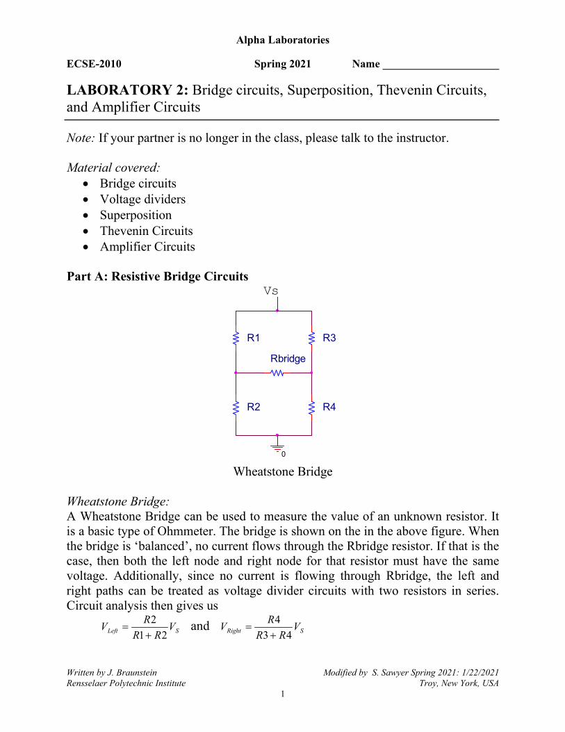
R1 R3
Rbridge
R2 R4
0
Vs
Wheatstone Bridge
Wheatstone Bridge: A Wheatstone Bridge can be used to measure the value of an unknown resistor. It is a basic type of Ohmmeter. The bridge is shown on the in the above figure. When the bridge is ‘balanced’, no current flows through the Rbridge resistor. If that is the case, then both the left node and right node for that resistor must have the same voltage. Additionally, since no current is flowing through Rbridge, the left and right paths can be treated as voltage divider circuits with two resistors in series. Circuit analysis then gives us
SLeft VRR
RV21
2+
= and SRight VRR
RV43
4+
=
Alpha Laboratories
ECSE-2010 Spring 2021 Name _____________________
Written by J. Braunstein Modified by S. Sawyer Spring 2021: 1/22/2021 Rensselaer Polytechnic Institute Troy, New York, USA
2
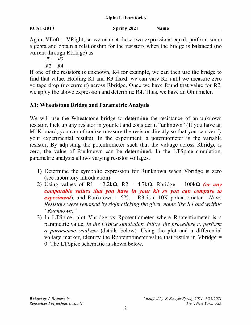
Again VLeft = VRight, so we can set these two expressions equal, perform some algebra and obtain a relationship for the resistors when the bridge is balanced (no current through Rbridge) as
43
21
RR
RR
=
If one of the resistors is unknown, R4 for example, we can then use the bridge to find that value. Holding R1 and R3 fixed, we can vary R2 until we measure zero voltage drop (no current) across Rbridge. Once we have found that value for R2, we apply the above expression and determine R4. Thus, we have an Ohmmeter. A1: Wheatstone Bridge and Parametric Analysis
We will use the Wheatstone bridge to determine the resistance of an unknown resistor. Pick up any resistor in your kit and consider it “unknown” (If you have an M1K board, you can of course measure the resistor directly so that you can verify your experimental results). In the experiment, a potentiometer is the variable resistor. By adjusting the potentiometer such that the voltage across Rbridge is zero, the value of Runknown can be determined. In the LTSpice simulation, parametric analysis allows varying resistor voltages.
1) Determine the symbolic expression for Runknown when Vbridge is zero (see laboratory introduction).
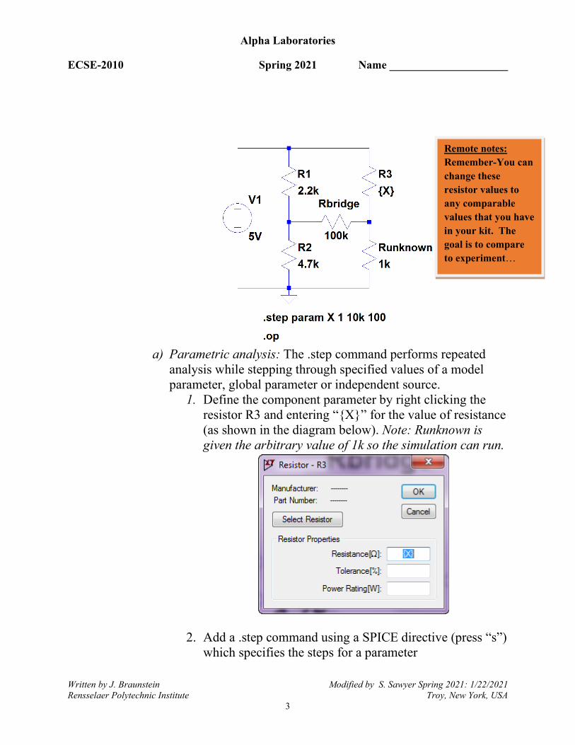
2) Using values of R1 = 2.2kΩ, R2 = 4.7kΩ, Rbridge = 100kΩ (or any comparable values that you have in your kit so you can compare to experiment), and Runknown = ???. R3 is a 10K potentiometer. Note: Resistors were renamed by right clicking the given name like R4 and writing “Runknown.”
3) In LTSpice, plot Vbridge vs Rpotentiometer where Rpotentiometer is a parametric value. In the LTpice simulation, follow the procedure to perform a parametric analysis (details below). Using the plot and a differential voltage marker, identify the Rpotentiometer value that results in Vbridge = 0. The LTSpice schematic is shown below.
Alpha Laboratories
ECSE-2010 Spring 2021 Name _____________________
Written by J. Braunstein Modified by S. Sawyer Spring 2021: 1/22/2021 Rensselaer Polytechnic Institute Troy, New York, USA
3
a) Parametric analysis: The .step command performs repeated
analysis while stepping through specified values of a model parameter, global parameter or independent source.
1. Define the component parameter by right clicking the resistor R3 and entering “X” for the value of resistance (as shown in the diagram below). Note: Runknown is given the arbitrary value of 1k so the simulation can run.
2. Add a .step command using a SPICE directive (press “s”)
which specifies the steps for a parameter
Remote notes: Remember-You can change these resistor values to any comparable values that you have in your kit. The goal is to compare to experiment…
Alpha Laboratories
ECSE-2010 Spring 2021 Name _____________________
Written by J. Braunstein Modified by S. Sawyer Spring 2021: 1/22/2021 Rensselaer Polytechnic Institute Troy, New York, USA
4
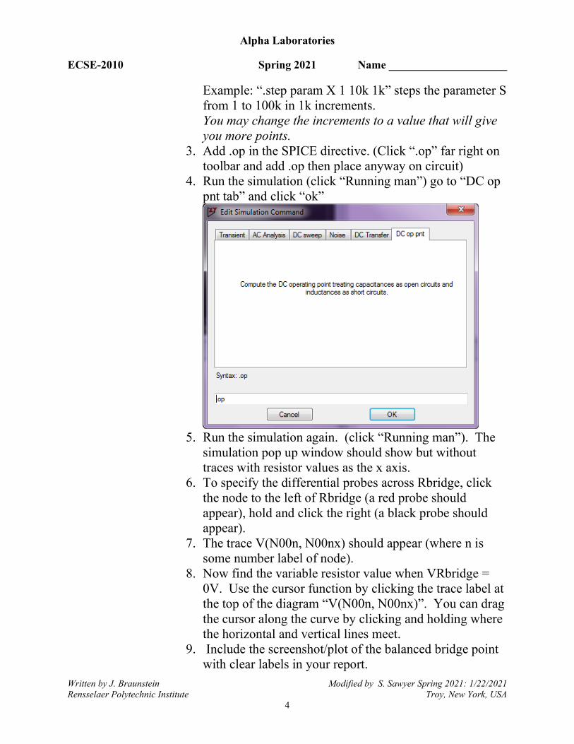
Example: “.step param X 1 10k 1k” steps the parameter S from 1 to 100k in 1k increments. You may change the increments to a value that will give you more points.
3. Add .op in the SPICE directive. (Click “.op” far right on toolbar and add .op then place anyway on circuit)
4. Run the simulation (click “Running man”) go to “DC op pnt tab” and click “ok”
5. Run the simulation again. (click “Running man”). The
simulation pop up window should show but without traces with resistor values as the x axis.
6. To specify the differential probes across Rbridge, click the node to the left of Rbridge (a red probe should appear), hold and click the right (a black probe should appear).
7. The trace V(N00n, N00nx) should appear (where n is some number label of node).
8. Now find the variable resistor value when VRbridge = 0V. Use the cursor function by clicking the trace label at the top of the diagram “V(N00n, N00nx)”. You can drag the cursor along the curve by clicking and holding where the horizontal and vertical lines meet.
9. Include the screenshot/plot of the balanced bridge point with clear labels in your report.
Alpha Laboratories
ECSE-2010 Spring 2021 Name _____________________
Written by J. Braunstein Modified by S. Sawyer Spring 2021: 1/22/2021 Rensselaer Polytechnic Institute Troy, New York, USA
5
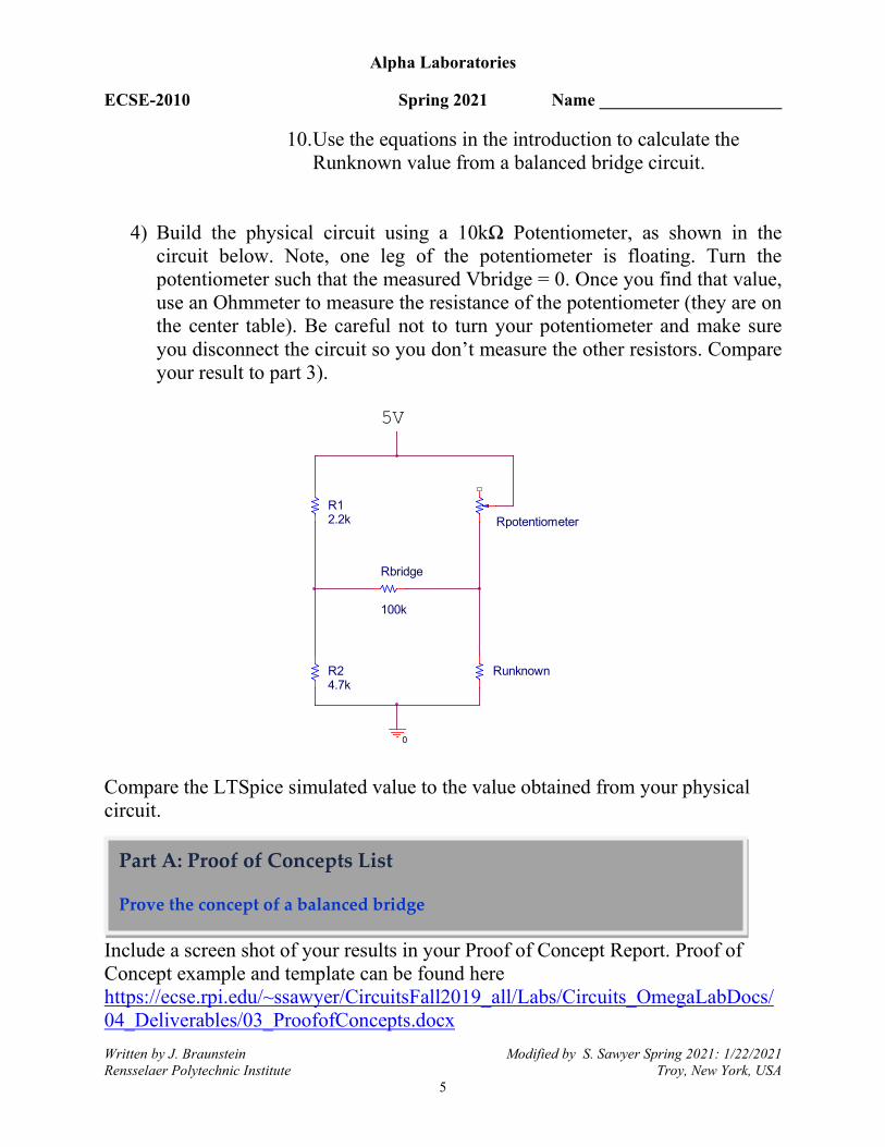
10. Use the equations in the introduction to calculate the Runknown value from a balanced bridge circuit.
4) Build the physical circuit using a 10kΩ Potentiometer, as shown in the circuit below. Note, one leg of the potentiometer is floating. Turn the potentiometer such that the measured Vbridge = 0. Once you find that value, use an Ohmmeter to measure the resistance of the potentiometer (they are on the center table). Be careful not to turn your potentiometer and make sure you disconnect the circuit so you don’t measure the other resistors. Compare your result to part 3).
R12.2k
Runknown
Rbridge
100k
R24.7k
Rpotentiometer
0
5V
Compare the LTSpice simulated value to the value obtained from your physical circuit. Include a screen shot of your results in your Proof of Concept Report. Proof of Concept example and template can be found here https://ecse.rpi.edu/~ssawyer/CircuitsFall2019_all/Labs/Circuits_OmegaLabDocs/04_Deliverables/03_ProofofConcepts.docx
Part A: Proof of Concepts List
Prove the concept of a balanced bridge
Alpha Laboratories
ECSE-2010 Spring 2021 Name _____________________
Written by J. Braunstein Modified by S. Sawyer Spring 2021: 1/22/2021 Rensselaer Polytechnic Institute Troy, New York, USA
6
LTSpice – Differential vs Nodal Measurements:
In the simulations we have done with LTSpice, we have used nodal measurements which provides the voltage at a node relative to the designated ground. In order to determine the voltage across a component, we then found the voltage difference between the two nodes associated with that component. In practice, measuring the voltage across a component where neither of the nodes is connected to ground can be problematic. To safely make those kind of measurements, we use differential probes. Fortunately for us, the Discovery Board only makes differential measurements.
Part B: Analog Discovery Board Variable Sources and Superposition Discovery Board – Variable Sources:
In the last laboratory, we used the fixed 5V supply. This source is constant. If we want to vary the source voltage, we need to use the function generator channels instead. There are two channels available, labelled W1 (yellow wire) and W2 (yellow striped wire) on the Discovery Board. To access the software, when you bring up the Waveforms main menu a. Select WaveGen, the second item under the Welcome settings. b. We will want to use both Channels at various times during the course.
(When we use only one Channel, you can turn off the other one if you want more space on your Desktop.) To enable both Channels, click on “Channels” pull down menu. Select both Channel 1 (AWG1) and Channel 2 (AWG2) such that there are check marks by both. Your window will probably refresh.
c. We will use DC sources for now. Select the straight line from the column of waveform shapes (it should be the first icon).
d. Go to the Offset pull down menu and set the DC voltage level. e. To output the voltage on the W1 (AWG1) wire, you need to select
make sure the Channel is both Enabled and running. In the upper right of the window, make sure “Enabled” is checked. Click Run.
f. Repeat steps c.-f. for AWG2
Alpha Laboratories
ECSE-2010 Spring 2021 Name _____________________
Written by J. Braunstein Modified by S. Sawyer Spring 2021: 1/22/2021 Rensselaer Polytechnic Institute Troy, New York, USA
7
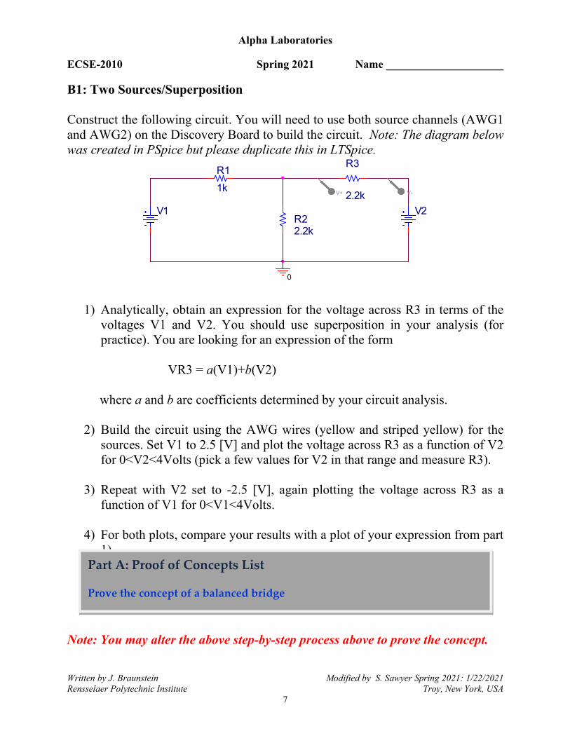
B1: Two Sources/Superposition Construct the following circuit. You will need to use both source channels (AWG1 and AWG2) on the Discovery Board to build the circuit. Note: The diagram below was created in PSpice but please duplicate this in LTSpice.
V1 V2
R11k
R22.2k
R3
2.2kV+
0
V-
1) Analytically, obtain an expression for the voltage across R3 in terms of the voltages V1 and V2. You should use superposition in your analysis (for practice). You are looking for an expression of the form
VR3 = a(V1)+b(V2)
where a and b are coefficients determined by your circuit analysis.
2) Build the circuit using the AWG wires (yellow and striped yellow) for the sources. Set V1 to 2.5 [V] and plot the voltage across R3 as a function of V2 for 0<V2<4Volts (pick a few values for V2 in that range and measure R3).
3) Repeat with V2 set to -2.5 [V], again plotting the voltage across R3 as a function of V1 for 0<V1<4Volts.
4) For both plots, compare your results with a plot of your expression from part 1).
Note: You may alter the above step-by-step process above to prove the concept.
Part A: Proof of Concepts List
Prove the concept of a balanced bridge
Alpha Laboratories
ECSE-2010 Spring 2021 Name _____________________
Written by J. Braunstein Modified by S. Sawyer Spring 2021: 1/22/2021 Rensselaer Polytechnic Institute Troy, New York, USA
8
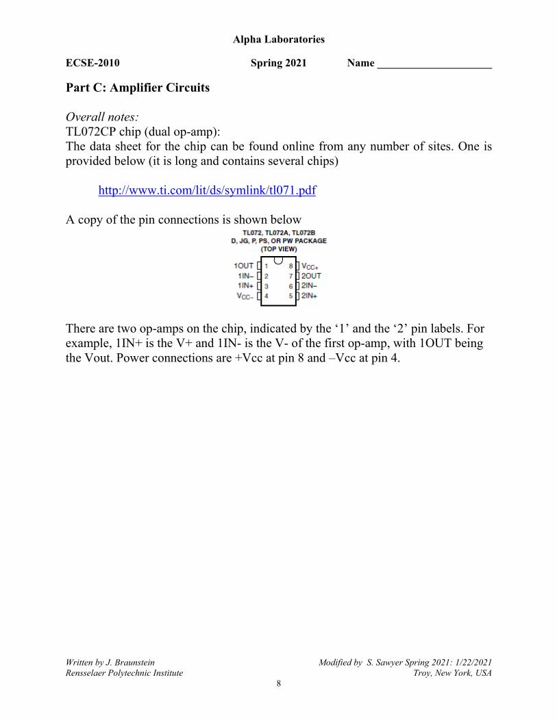
Part C: Amplifier Circuits Overall notes: TL072CP chip (dual op-amp): The data sheet for the chip can be found online from any number of sites. One is provided below (it is long and contains several chips)
http://www.ti.com/lit/ds/symlink/tl071.pdf A copy of the pin connections is shown below
There are two op-amps on the chip, indicated by the ‘1’ and the ‘2’ pin labels. For example, 1IN+ is the V+ and 1IN- is the V- of the first op-amp, with 1OUT being the Vout. Power connections are +Vcc at pin 8 and –Vcc at pin 4.
Alpha Laboratories
ECSE-2010 Spring 2021 Name _____________________
Written by J. Braunstein Modified by S. Sawyer Spring 2021: 1/22/2021 Rensselaer Polytechnic Institute Troy, New York, USA
9
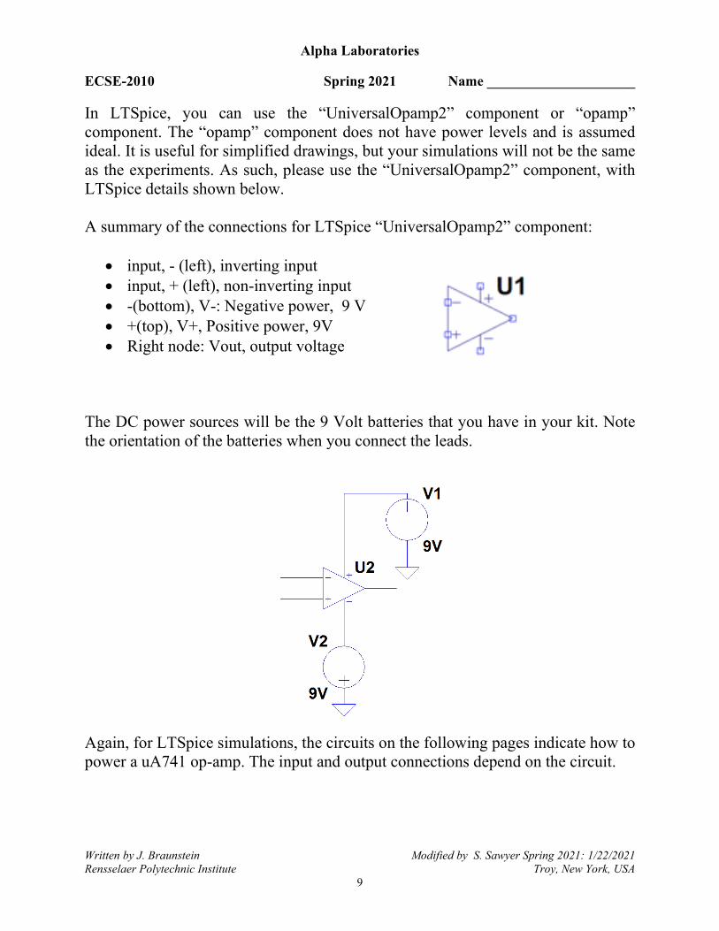
In LTSpice, you can use the “UniversalOpamp2” component or “opamp” component. The “opamp” component does not have power levels and is assumed ideal. It is useful for simplified drawings, but your simulations will not be the same as the experiments. As such, please use the “UniversalOpamp2” component, with LTSpice details shown below. A summary of the connections for LTSpice “UniversalOpamp2” component:
• input, - (left), inverting input • input, + (left), non-inverting input • -(bottom), V-: Negative power, 9 V • +(top), V+, Positive power, 9V • Right node: Vout, output voltage
The DC power sources will be the 9 Volt batteries that you have in your kit. Note the orientation of the batteries when you connect the leads.
Again, for LTSpice simulations, the circuits on the following pages indicate how to power a uA741 op-amp. The input and output connections depend on the circuit.
Alpha Laboratories
ECSE-2010 Spring 2021 Name _____________________
Written by J. Braunstein Modified by S. Sawyer Spring 2021: 1/22/2021 Rensselaer Polytechnic Institute Troy, New York, USA
10
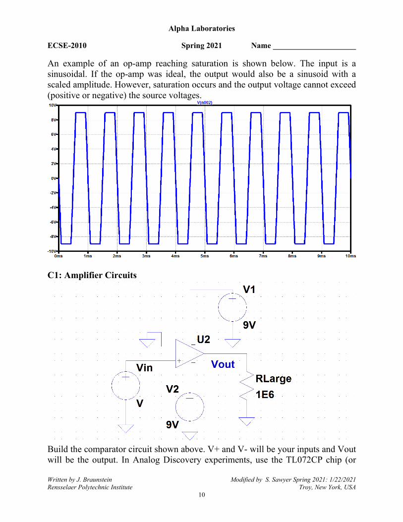
An example of an op-amp reaching saturation is shown below. The input is a sinusoidal. If the op-amp was ideal, the output would also be a sinusoid with a scaled amplitude. However, saturation occurs and the output voltage cannot exceed (positive or negative) the source voltages.
C1: Amplifier Circuits
Build the comparator circuit shown above. V+ and V- will be your inputs and Vout will be the output. In Analog Discovery experiments, use the TL072CP chip (or
Alpha Laboratories
ECSE-2010 Spring 2021 Name _____________________
Written by J. Braunstein Modified by S. Sawyer Spring 2021: 1/22/2021 Rensselaer Polytechnic Institute Troy, New York, USA
11
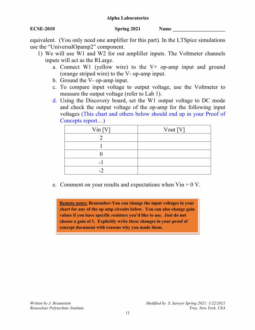
equivalent. (You only need one amplifier for this part). In the LTSpice simulations use the “UniversalOpamp2” component.
1) We will use W1 and W2 for out amplifier inputs. The Voltmeter channels inputs will act as the RLarge.
a. Connect W1 (yellow wire) to the V+ op-amp input and ground (orange striped wire) to the V- op-amp input.
b. Ground the V- op-amp input. c. To compare input voltage to output voltage, use the Voltmeter to
measure the output voltage (refer to Lab 1). d. Using the Discovery board, set the W1 output voltage to DC mode
and check the output voltage of the op-amp for the following input voltages (This chart and others below should end up in your Proof of Concepts report…)
e. Comment on your results and expectations when Vin = 0 V.
Vin [V] Vout [V] 2 1 0 -1 -2
Remote notes: Remember-You can change the input voltages in your chart for any of the op amp circuits below. You can also change gain values if you have specific resistors you’d like to use. Just do not choose a gain of 1. Explicitly write these changes in your proof of concept document with reasons why you made them.

Alpha Laboratories
ECSE-2010 Spring 2021 Name _____________________
Written by J. Braunstein Modified by S. Sawyer Spring 2021: 1/22/2021 Rensselaer Polytechnic Institute Troy, New York, USA
12
2) In LTSpice, build the comparator circuit using a UniveralOpamp2 op-amp.
You will need to add a load resistor at the output node since LTSpice does not allow nodes to float (be unconnected). A 1E6Ω load is fine (use exponential notation since M in LTspice is 1E-3). Compare the output voltages between LTSpice and Analog Discovery. You should see some differences, what causes these differences?
Vin [V] Vout [V] 2 1 0 -1 -2
Alpha Laboratories
ECSE-2010 Spring 2021 Name _____________________
Written by J. Braunstein Modified by S. Sawyer Spring 2021: 1/22/2021 Rensselaer Polytechnic Institute Troy, New York, USA
13
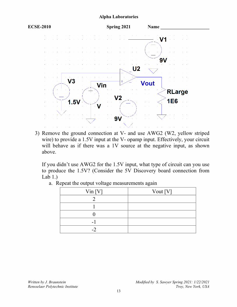
3) Remove the ground connection at V- and use AWG2 (W2, yellow striped
wire) to provide a 1.5V input at the V- opamp input. Effectively, your circuit will behave as if there was a 1V source at the negative input, as shown above. If you didn’t use AWG2 for the 1.5V input, what type of circuit can you use to produce the 1.5V? (Consider the 5V Discovery board connection from Lab 1.)
a. Repeat the output voltage measurements again
Vin [V] Vout [V] 2 1 0 -1 -2
Alpha Laboratories
ECSE-2010 Spring 2021 Name _____________________
Written by J. Braunstein Modified by S. Sawyer Spring 2021: 1/22/2021 Rensselaer Polytechnic Institute Troy, New York, USA
14
4) Again, compare your Analog Discovery experiment to the LTSpice simulation.
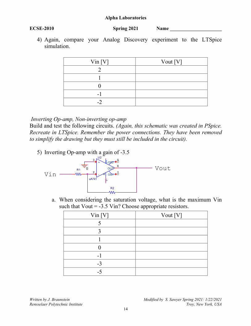
Inverting Op-amp, Non-inverting op-amp Build and test the following circuits. (Again, this schematic was created in PSpice. Recreate in LTSpice. Remember the power connections. They have been removed to simplify the drawing but they must still be included in the circuit).
5) Inverting Op-amp with a gain of -3.5 U2
uA741
+3
-2
V+7
V-4
OUT6
OS11
OS25
VoutVin
0
R2
R1
a. When considering the saturation voltage, what is the maximum Vin
such that Vout = -3.5 Vin? Choose appropriate resistors.
Vin [V] Vout [V] 2 1 0 -1 -2
Vin [V] Vout [V] 5 3 1 0 -1 -3 -5

Alpha Laboratories
ECSE-2010 Spring 2021 Name _____________________
Written by J. Braunstein Modified by S. Sawyer Spring 2021: 1/22/2021 Rensselaer Polytechnic Institute Troy, New York, USA
15
b. Build the circuit in LTSpice and verify that simulation is constant with experiment (within the limits of the respective saturation voltages).
6) Non-Inverting Op-amp with a gain of 3
Build, simulate, and test a circuit you create. Come up with a simple chart of inputs and record output.
Include screen shots of your LTSpice, Experimental, and Analytical results in your Proof of Concept Report. Part D: Alpha Laboratories Applications
1) You will have an opportunity in class/lab to discuss and design a circuit that includes components learned throughout Unit 1. Draw high level design blocks including input and output for each block based on the Building Block components Lab Requirements: Building Blocks (scroll down to page 10) that include:
1. at least one input stage components, 2. two Milestone 1 stage components, 3. and at least one output stage component.
2) Simulate each individual building block and describe how it should behave in your circuit. Each high level design block from 1) should have an associated schematic created in LTSpice or equivalent. Then the simulation output should be shown. Highlight how the output you are showing becomes the correct input for the next stage. (You do not need to build this circuit.)
Part C: Proof of Concepts List
Prove the function of a comparator op amp circuit (0V reference) Prove the function of a comparator op amp circuit (1.5V reference) Prove the function of an inverting op amp circuit (gain -3.5) Prove the function of a non-inverting op amp circuit (gain of 3)
Alpha Laboratories
ECSE-2010 Spring 2021 Name _____________________
Written by J. Braunstein Modified by S. Sawyer Spring 2021: 1/22/2021 Rensselaer Polytechnic Institute Troy, New York, USA
16
Include screen shots of your LTSpice, Experimental, and Analytical results in your Proof of Concept Report. (You do not need to build this circuit. Be sure to discuss what happened when you tried to connect your building blocks. Did it work? Did it not work as expected? If not, speculate why didn’t it work. EXTRA CREDIT: Write in your metacognition journal (instructions and template in the link below, feel free to continue to edit a Google doc throughout the course to add entries).
https://ecse.rpi.edu/~ssawyer/CircuitsFall2019_all/Labs/Circuits_OmegaLabDocs/04_Deliverables/05_Circuits_Metacognition%20and%20Reflections.docx
SUMMARY of Concepts Concept List that must be accounted for in your Proof of Concepts PART A: 1. Prove the concept of a balance bridge PART B: 1. Prove the superposition concept PART C: 1. Prove the function of a comparator op amp circuit (0V reference) 2. Prove the function of a comparator op amp circuit (1.5V reference) 3. Prove the function of an inverting op amp circuit (gain -3.5) 4. Prove the function of a non-inverting op amp circuit (gain of 3) PART D: Alpha Labs Applications 1. Prove that your individual design blocks with your given input resulted in the correct output for the next stage of your design.
Part D: Proof of Concepts List
Prove that your individual design blocks with your given input resulted in the correct output for the next design stage. (You can make assumptions and replacements for sensors like an LDR is analogous to a potentiometer with a varying resistance)