Embed Size (px)
Citation preview

ES 3 Laboratory #4 Page 1 of 14
ES 3: Introduction to Electrical Systems
Laboratory 4: Amplification, Impedance, and Frequency Response
I. GOALS: In this laboratory, you will build an audio amplifier using an LM386 integrated circuit. The amplifier will increase the voltage of a very weak signal, and the output of the amplifier will drive an audio speaker. This is an example of a complete electrical system. You will be asked to determine the Thevenin equivalent resistance of the amplifier chip, as a way of reviewing the material covered in Lab #3. In addition, you will use the oscilloscope to measure the amount by which the amplifier increases the weak input signal (the gain). Finally, you will measure the gain for a wide range of input signal frequencies. From this data, you can report the frequency response of the amplifier circuit by constructing a Bode plot using Excel. After the laboratory, you will perform a theoretical analysis of the amplifier circuit. II. PRE-LAB QUESTIONS: Read the laboratory manual in its entirety and be certain that you understand the experiments that need to be completed. In this lab, you will use a breadboard to prototype a somewhat more complicated circuit. Review the use of the breadboard (Lab #3). What is the impedance (in ohms) of a 0.01 μF capacitor at the following frequencies? 10 Hz = 62.8 rad/sec 100 Hz 1 kHz
10 kHz III. EXPERIMENTS: In this laboratory, you will build an audio amplifier and measure its gain and frequency response. The voltage gain of an amplifier is simply the ratio of the output signal voltage to the input signal voltage:
)/( voltvoltsvvA
in
outV = Eq. 1
In electrical engineering, gain is often expressed in decibels (dB). The gain in dB is found by taking log10 of the ratio in Eq. 1 and multiplying by 20:

ES 3 Laboratory #4 Page 2 of 14
)(log20 10 dBvvA
in
outV ⎟⎟
⎠
⎞⎜⎜⎝
⎛= Eq. 2
Notice that if vout=vin, then the gain is AV = 1 (v/v) = 0 dB. If the output signal is 100 times larger than the input signal, then the gain is AV= 100 v/v or 20log10(100) = 40 dB. Ideally, a perfect amplifier would have the same voltage gain for every conceivable input signal. In reality, however, the gain of an amplifier always drops to zero for very high frequency signals. Many amplifiers also exhibit poor gain at low frequency. The variation of gain as a function of frequency is called the frequency response: AV(f) vs. f. The first task of this experiment is to build an audio amplifier using the LM386 integrated circuit (IC). This IC contains approximately 25 circuit elements such as resistors, transistors and diodes (see Section V.3 for the internal circuit). It is difficult to miniaturize capacitors, so the amplifier circuit shown in Figure 1 requires three external capacitors in addition to the LM386 chip.
100uF
sCC
Functiongenerator
9v
100uF
sCC
Functiongenerator
9v
Figure 1. An amplifier circuit that uses the LM386 chip
The circuit symbol for an amplifier is a triangle. The input(s) to an amplifier are drawn on the broad side of the triangle (pins 2 and 3), and the output is drawn at the vertex of the triangle (pin 5). All amplifiers require an external power source. This power supply is applied to pins 6 and 4 of the LM386. We will use a 9 volt battery as the power source. Note: Pins 1, 7, and 8 are not used in this particular circuit. Amplifiers increase the voltage (or current, or power) of a weak input signal. Examples of devices that produce weak signals requiring amplification include microphones, strain gauges, pH sensors, and antennas. In this experiment, we will replace the signal device by a function generator. This substitution will allow you to apply a well-behaved input signal to the amplifier. The function generator is connected to the amplifier’s input (pin 3) through a coupling capacitor CC. The coupling capacitor blocks unwanted DC voltages (ω=0) from entering the amplifier because the impedance of a capacitor is infinity as ω 0 (i.e., an open circuit):
circuitopenanCj
ZC ...1lim||lim00
∞==→→ ωωω
Eq. 3

ES 3 Laboratory #4 Page 3 of 14
The 100μF capacitor connected to the output of the amplifier chip (pin 5) performs the same function as CC: it blocks unwanted DC voltage from reaching the speaker. Why would we want to block DC voltages? DC voltages do not produce any sound; only time-varying signals produce audible sound. A constant voltage applied to the speaker will dissipate power, however, and this power is simply wasted because no sound is produced. Figure 1 shows the amplifier circuit in an abbreviated style. This style is used to simplify the appearance of the schematic, but it can be tricky to understand at first. Figure 2 shows the same circuit drawn in a more complete and familiar fashion. Of particular importance is the numbering of the pins of the IC. The IC has a small mark either near pin 1 or at the top of the chip. These two marks are shown on the LM386 in Figure 2. The pins are then numbered sequentially in a counter-clockwise direction. You should now build the amplifier circuit on a breadboard. Use a coupling capacitor with CC=0.01μF. Connect the battery last, after you have double-checked that the circuit is correctly wired. Make certain that the IC straddles the deep groove in the breadboard such that pins 1-4 are connected to the tie points to the left of the groove and pins 5-8 are connected to the tie points to the right of the groove. Please refer to the photographs of the circuit in Section V if you require additional help.
LM 386
1
2
3
4
8
7
6
5
9 V
+
0.047uF10 Ω
100 uF
(ground)
Spkr16 Ω
OscilloscopeProbe:
VOUT
Functiongenerator
0.025sin(ωt) v
-
CC
OscilloscopeProbe:
VIN
LM 386
1
2
3
4
8
7
6
5
9 V
+
0.047uF10 Ω
100 uF
(ground)
Spkr16 Ω
OscilloscopeProbe:
VOUT
Functiongenerator
0.025sin(ωt) v
-
CC
OscilloscopeProbe:
VIN
Figure 2. A complete schematic of the amplifier circuit shown in Fig. 1
Measure and record the resistance or capacitance for all of the components used in the amplifier circuit: R10=____Ω; CC=____μF; C100=____μF; C047=____μF; Rspkr=____Ω In this experiment, the function generator needs to produce a very small voltage. This requires pressing the [ATT-20dB] button and gently pulling the AMPL knob out. Each of these actions reduces the output voltage by 20dB for a total attenuation of -40dB. In this experiment you should set the function generator to produce a 1000 Hz sinusoid with a peak-to-peak amplitude of 50 mV: vin(t) = 0.025sin(2π.1000t) volts Eq. 4

ES 3 Laboratory #4 Page 4 of 14
Voltage Gain Using the two channels of the oscilloscope, measure vin and vout as shown in Figure 2. Report the measured values in your lab report and calculate the voltage gain of the amplifier using both (v/v) and (dB). Check: The LM386 should have a voltage gain of approximately 20 v/v. Next, find the Thevenin equivalent resistance of the LM386 amplifier (f =1kHz) by measuring the output voltage of the amplifier with the speaker disconnected (this is the open circuit voltage). Repeat the measurement of vout with the speaker re-connected. Report these two measurements. In your lab report, calculate RTH of this amplifier using the methodology that you learned in Laboratory #3. VOC = ______vp-p Vspkr = ______vp-p RTH(amp)=___________Ω Note: RTH(amp)<<16 Ω, so the output voltage only changes by a small amount. Frequency Response of the Amplifier In this section, you will determine the gain of the amplifier as the input frequency is varied over audio frequencies (20 Hz – 10 kHz). During these measurements, it is critical to maintain a constant input voltage, vin = 0.025sinωt. Complete Table 1 with measurements of the output voltage for each frequency listed. Next, double the capacitance of CC to 0.02 μF by adding a second 0.01μF capacitor in parallel with the original CC. Repeat the measurements of vout vs. f.
Table 1. Use this table to record the frequency response of the LM386 amplifier circuit for CC = 0.01 μF and CC = 0.02 μF
Frequency (Hz)
vin (volts, pk-pk)
vout (volts, pk-pk) CC = 0.01 μF
vout (volts, pk-pk) CC = 0.02 μF
20 0.05 50 0.05 100 0.05 200 0.05 500 0.05 1000 0.05 2000 0.05 5000 0.05 10000 0.05

ES 3 Laboratory #4 Page 5 of 14
Frequency response data is usually plotted in a special format called a Bode diagram or Bode plot (pronounced bow-dee). A Bode plot is a graph of the amplifier gain in decibels (dB) versus the input frequency. The frequency scale, however, is a logarithmic axis, rather than a linear scale. Read the instructions in Section V to learn how to use Excel to create a Bode plot. Include a graph in your lab report that shows the frequency response of this amplifier as a Bode plot. Include both sets of data (CC = 0.01 and 0.02 μF) on the same plot. Describe why changing CC also changes the behavior of the circuit at low frequencies. IV. LAB REPORT: All required data, questions, and written comments can be found within the framed text blocks. Tabulate or plot all of the requested data and answer the questions in a manner that flows naturally. Complete Lab Report Guidelines are listed on the course website. In addition, include a theoretical analysis of the amplifier’s frequency response as outlined below. Theoretical analysis of frequency response From the experiments in this lab, you have observed that the gain of this particular amplifier decreases as the frequency approaches zero. There are two components that are responsible for the poor low frequency response:
(1) The coupling capacitor (CC) blocks low frequency signals because the impedance of CC goes to infinity. This effectively disconnects the function generator from the amplifier’s input (pin 3) for low frequency signals.
(2) The 100μF capacitor between the output of the amplifier and the speaker also looks like an open circuit as f 0. This effectively disconnects the speaker from the amplifier for low frequency signals.
Both of these phenomena are known as “high-pass filters.” That is, the part of the circuit consisting of a capacitor and a resistor blocks low frequencies, but allows high frequencies to pass. The boundary between blocking and passing signals at the input depends on the value of CC and the input resistance of the amplifier (RIN). In the lab, you doubled the capacitance of CC from 0.01μF to 0.02μF. This reduced the impedance of CC by half and improved the ability of low frequency signals to reach the input of the amplifier. In this section, you are asked to provide the theoretical analysis. Remember from Laboratory #3 that the model for a generic amplifier consists of an input resistance (RIN), a dependent voltage source that models gain (AV), and a Thevenin equivalent output resistance, Rth(amp), as shown in Figure 3. You should already know

ES 3 Laboratory #4 Page 6 of 14
the value of Rth(amp) and AV from previous experiments in this lab. The manufacturer tells us that RIN is 50kΩ, although this value varies substantially from chip to chip.
+
-
+-
RIN
=50kΩ
+
VIN
-
AVVx(AV ~ 20at f=1kHz)
=(0.025)sin(ωt)
Rth(F.G.)= 50 Ω
Rth(amp)
Rspkr
=16 Ω
Function Generator Model Amplifier Model Speaker Model
CC
+
VX
-
100uF
+
-
+-
RIN
=50kΩ
+
VIN
-
AVVx(AV ~ 20at f=1kHz)
=(0.025)sin(ωt)
Rth(F.G.)= 50 Ω
Rth(amp)
Rspkr
=16 Ω
Function Generator Model Amplifier Model Speaker Model
CC
+
VX
-
100uF
Figure 3. A circuit that models the behavior of the function generator, amplifier, and speaker.
Furthermore, you have already deduced the TEC for the function generator in Lab #3. Finally, the model for the speaker is 16Ω. In this analysis, we will ignore the speaker’s inductance because ωL is small at low frequencies, according to Lab #2. We know that VIN = 0.025sin(ωt), but it is necessary to find VX to solve the circuit shown in Figure 3. This circuit is a simple voltage divider, so VX is given by:
)1( CIN
ININX CjR
RVVω+
= Eq. 5
In the lab, you measured the amplitude (magnitude) of the voltage. Therefore, in order to compare your lab results with theory, it is necessary to find the magnitude of VX. Show that |VX| is given by:
1)(025.0
)1(||||
2 +=
+=
CIN
CIN
CIN
ININX
CRCR
CjRRVV
ωω
ω Eq. 6
Notice that as the frequency goes to zero in Eq. 6, the voltage VX also goes to zero. This is due to the blocking of low frequencies by the capacitor CC.

ES 3 Laboratory #4 Page 7 of 14
Now that we know VX, it is possible to find the voltage produced by the dependent voltage source: VOC = AVOVX. You may use the value of AVO that you found experimentally at f=1 kHz. This is called the midband gain, AVO ~ 20 v/v. Lastly, we will make a simplifying assumption that neither the speaker’s inductance nor the coupling capacitor between the amplifier and the speaker affects the frequency response.1 Ignoring the capacitor leaves us with a simple resistive voltage divider at the amplifier’s output (pin 5) between RTH(amp) and RSPKR:
)(ampRRR
VAVTHSPKR
SPKRXVOout +
= Eq. 7
)(1)(025.0
)(||||
2 ampRRR
CR
CRA
ampRRR
VAVTHSPKR
SPKR
CIN
CINVO
THSPKR
SPKRXVOout +
⋅+
⋅=+
=ω
ω
Eq. 8 Equation 8 is the zero-to-peak output voltage as a function of radian frequency, ω. Dividing Eq. 8 by the amplitude of the input voltage (0.025 v0-pk) gives an expression for the gain as a function of frequency. This is the frequency response, |AV(ω)|. Use Excel and the measurements from your lab report to create a Bode plot of the theoretical frequency response of your amplifier (remember: ω=2πf). Compare the theoretical result with your measured result and describe the potential sources of any errors.
1 Although, if this capacitor is small and the speaker resistance is small there is a significant additional attenuation of the low frequency gain.
ES 3 Laboratory #4 Page 8 of 14
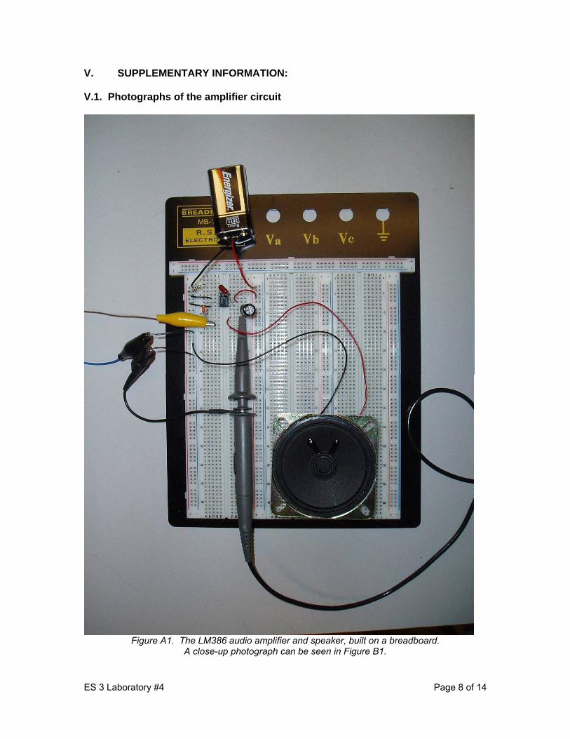
V. SUPPLEMENTARY INFORMATION: V.1. Photographs of the amplifier circuit
Figure A1. The LM386 audio amplifier and speaker, built on a breadboard.
A close-up photograph can be seen in Figure B1.

ES 3 Laboratory #4 Page 9 of 14
Figure B1. A close-up view of the breadboard connections in Fig. A1
To spkr
To 9v (+)
This column contains all of the ground connections
Function Gen. S
cope
To 9v (-)
CC

ES 3 Laboratory #4 Page 10 of 14
V.2. Creating a Bode Plot of the Amplifier’s Gain (magnitude only) Begin by tabulating the output voltage (pk-pk) as a function of input frequency for both CC = 0.01 μF and CC = 0.02 μF (see columns A,B, and D in Figure A2.) Next copy the frequency column to column H; To create data for the amplifier gain use the expression that
Gain = 20log(Vout/Vin) where Vin = 0.05 volts (pk-pk) Create the gain in cell I3 by clicking the cell and then entering the following expression in the fx window:
=20*LOG(B3/0.05) Then copy and paste this cell down the entire column. Repeat this procedure for the column of data taken with CC = 0.02μF using
=20*LOG(D3/0.05)
Figure A2. Excel Spreadsheet containing the output voltage vs. input frequency. The data to the
right side demonstrates how the Gain is computed. Follow the example seen in Figure B2 to make the Bode plot by choosing Insert>>Chart>> “XY scatter”. Then select the Data Range to include the Frequency data and both columns containing the Gain data (outlined by clicking and dragging the mouse).

ES 3 Laboratory #4 Page 11 of 14
Figure B2. Excel Spreadsheet showing Gain vs. Frequency data selected for insertion into a
chart Next, insert Titles and axis labels, including the units, as shown in Figure C2.
Figure C2. Excel Spreadsheet showing the selection of chart titles and axis labels

ES 3 Laboratory #4 Page 12 of 14
Notice how the low frequency data is crowded together. To fix this problem, a Bode plot uses a logarithmic frequency axis. To create this axis, Double-click the Frequency axis of the chart and change the scale to logarithmic as shown in Figure D2.
Figure D2. Excel Spreadsheet showing the conversion of the frequency axis from LINEAR to
LOGARITHMIC Finally, clean up the appearance of the graph by double clicking the Gain axis and resetting the Value (X) axis crosses to -10 (dB).
Figure E2. Excel Spreadsheet showing Gain vs. Frequency as a Bode Plot

ES 3 Laboratory #4 Page 13 of 14
Please remember to label each data set with the value of the coupling capacitor by inserting an appropriate Legend into the plot: Cc = 0.01uF and Cc = 0.02uF. Include this Bode plot of the amplifier’s frequency response in your lab report. V.3. Internal circuit of the LM386 audio amplifier chip

ES 3 Laboratory #4 Page 14 of 14
VI. PARTS LIST: LM386 audio amplifier chip 100μF non polarized electrolytic capacitor 0.047μF or 0.05 μF capacitor 0.01 μF capacitors (2 per group) 10 Ω resistor 16 ohm speaker with soldered wires 9 volt battery with battery clip Breadboard for prototyping circuits Function Generator (Instek, GFG-8250A) Oscilloscope (Tektronix TDS 2012, or equivalent) with 2 probes LCR meter (Stanford Research Systems Model 715), one unit per room. Test Leads: BNC-to-Alligator clips (1) Wires with Alligator clips (2) Banana plug-to-Alligator clips (2) Hook-up wire for breadboards