Embed Size (px)
Citation preview

Department of Electrical Engineering
College of Engineering
University of Hail
Laboratory Manual
EE 303 – Electronics II
2017-171

EE 303 (Electronics II) Lab Manual II
Table of Contents
Preface .................................................................................................................................... III
Introduction ........................................................................................................................... IV
Safety Tips ............................................................................................................................... V
Tutorial #1: Net Listing and Simulation Analysis Using PSPICE ...................................... 1
Tutorial #2: Transistor Models for PSPICE ......................................................................... 9
Experiment #1: Gain Frequency Characteristics of Single Transistor Amplifiers ......... 18
Experiment #2: Gain Frequency Characteristics of Multistage Transistor Amplifiers .. 20
Experiment #3: Linear Applications of Operational Amplifiers ....................................... 22
Experiment #4: Determination of Operational Amplifier Characteristics ...................... 25
Experiment #5: Active Filters ............................................................................................... 30
Experiment #6: Feedback and Non-linear Distortion ........................................................ 34
Experiment #7: Feedback Amplifiers .................................................................................. 38
Experiment #8: Oscillators.................................................................................................... 40

EE 303 (Electronics II) Lab Manual III
Preface
This manual contains laboratory experiments for the course “Electronics II” (EE 303). These
experiments are designed to support, verify and supplement the theory taught in the course
“Electronics II (EE 303)”. It will also help students gain a workable knowledge on design,
analysis and simulation of various basic analog electronic circuits such as amplifiers, filters,
oscillators, etc. which are essential circuit building blocks for any real life application.
Comments and suggestions are welcome from both instructors and students that will help in
designing new experiments or modifying the existing ones.
Muhammad Usman, Assistant Professor
EE 303 (Electronics II) Lab Manual IV
Introduction
The manual starts with two tutorials on PSPICE, in which the first tutorial shows the
simulation of circuits using simple Netlist command codes and then introduces the use of
advance models for transistor in PSPICE. After the end of these two tutorials, students are
expected to carry out the simulation of rest of the experiment circuits using Netlist command
codes.
There are total 8 experiments. The first two experiments deal with the frequency response of
transistor amplifier circuits. The third and the fourth deal the linear application and non-ideal
characteristics of operational amplifier. The rest of the experiments deal with the filters,
feedback and oscillator circuits.
Laboratory Guidelines:
Every week before lab, each student should read over the laboratory experiment and work out
the various calculations, etc. that are outlined in the prelab. The student should refer to
Microelectronic Circuits, 4th edition by Sedra and Smith for the fundamental theory.
The students should work as a group.
Most experiments have several parts; students must alternate in doing these parts as
they are expected to work in group.
Static sensitive devices should be handled carefully.
All equipment, apparatus and tools must be RETURNED to their original place after
use.
Students are NOT allowed to work alone in the laboratory.
Report immediately to the Lab Supervisor any damages to equipment, hazards, and
potential hazards.
Do not put suspected defective parts back in the bins. Give them to the Lab
Technician for testing or disposal.
Report all equipment problems to Lab Instructor or Lab Technician.
Each student must have a laboratory notebook. The notebook should be a permanent
document that is maintained and witnessed properly, and that contains accurate
records of all lab sessions.
Laboratory and equipment maintenance is the responsibility of not only the Lab
Technician, but also the students. A concerted effort to keep the equipment in
excellent condition and the working environment well-organized will result in a
productive and safe laboratory.
EE 303 (Electronics II) Lab Manual V
Safety Tips
It is the duty of all concerned who use the electrical laboratory to take all reasonable steps to
safeguard health and safety of themselves and the safety of the equipment they use.
Safety of Yourself:
Inspect all cords, plugs, and equipment for possible damage. Notify your instructor if
you notice any damage or any other trouble, such as, loose wall sockets or sparks.
Be careful when inserting or removing a plug. Do not remove the plugs by pulling on
the cord.
While making connections, keep the power off.
Do not touch bare wires or parts. If you have to do so, turn off all the power first and
unplug the equipment.
Do not work when your skin is wet.
Safety of Equipment:
Before plugging ICs into a board, be sure that their pins are straight.
Unplug ICs very carefully, to avoid bending the pins. You may want to try an IC
extractor if one is available in your lab.
Be aware of the fact that ICs, especially those made with MOS technology, can be
instantly damaged by static electricity, such as that accumulated by your body. You
should make sure you are "discharged" before handling them, by momentarily
touching the metal case of a properly grounded instrument.
Be sure capacitors are discharged before plugging them into a circuit. If in doubt,
short their leads.
When finished wiring a circuit, inspect all connections to make sure you have made
no mistakes. Turn on the circuit only when you are happy with the result.
If your circuit is connected to a signal generator (such as, function generator), do not
turn it on until after you have turned on the power supplies. If you later want to turn
off the power, turn off the signal source first.
Laboratory Ethics:
Do not eat, drink or smoke in the lab.
Do not use any equipment unless it is mentioned in the lab manual or otherwise
advised by the lab instructor to do so.
Switch off the equipment and disconnect the power supplies from the circuit before
leaving the laboratory.
Observe cleanliness and proper laboratory housekeeping of the equipment and other
related accessories.

EE 303 Lab Manual: Tutorial #1: Net Listing and Simulation Analysis Using PSPICE 1
Tutorial #1: Net Listing and Simulation Analysis Using PSPICE
Objective:
In this tutorial, the students will learn about PSPICE specially in net listing and simulation
analysis. There are three basic types of analysis: DC, Transient and AC analysis.
DC analysis allows you to see the behavior of the circuit in response to DC input
voltage/current.
Transient analysis displays the input-output waveforms as a function of time so you
can see if the signal is as expected or distorted.
AC analysis will show the behavior of the circuit as a function of frequency
(frequency response).
Figure 1
Additional number of SPICE commands in simulation analysis will be introduced and more
circuits will be tested.
Introduction:
An electronic circuit does not have to be very complex or contain many elements before the
hand calculation effort becomes unwieldy. In fact, for many of the examples worked in the
lectures we were forced to use a number of device-model approximations and circuit
simplifications. These circuit solutions are usually quite adequate for a first look; however,
for a more detailed design and analysis approach, Computer Aided Design (CAD) and
Computer Aided Engineering (CAE) tools are used.
Currently, one of the more widely used general purpose circuit simulation program for
industrial and academic computer systems is SPICE. As you know SPICE can be used to
simulate circuits containing resistors, capacitors, inductors, mutual inductors, independent
and dependent voltage and current sources, and basic semiconductor devices. In EE 203
students were using Schematic Editor of PSPICE to draw circuits and then run simulation
analysis. In fact, drawing circuits and ensuring correct interconnections may be time
consuming. Alternatively, circuits can be described in PSPICE by specifying their various
components and their terminal connections (net listing).
A typical PSPICE input file format is as follows:
TITLE STATEMENT
CIRCUIT ELEMENTS:
Power Supplies / Signal Sources
Simulation Experiment
DC Transient AC

EE 303 Lab Manual: Tutorial #1: Net Listing and Simulation Analysis Using PSPICE 2
Circuit description/Element Descriptions
Model Statement
CONTROL STATEMENTS:
Analysis Requests
Output Requests
.END
Notes: 1. The first line must be a title line which is usually reflects the file contents. It cannot be
omitted.
2. The last line must be the .END statement.
3. You can insert comment lines. Anytime a line starts with an "*", Pspice ignores the
whole line. Using an "*" is also handy to block out a command line.
4. You can use upper or lower case letters.
5. Don't forget to add a carriage return after the .END statement.
Control Statements:
.OP The inclusion of the statement .OP makes SPICE perform DC analysis to find the
operating point of the circuit and to print detailed results of the operating point
analysis. The general form is .OP
.DC
The inclusion of the statement .DC makes the spice perform the dc analysis of the
circuit over specified range of input. The general format is
.DC SOURCE_NAME START_VAL STOP-VAL INCREMENT_VAL
Where SOURCE_NAME is the name of an independent voltage or current source.
START_VAL, STOP_VAL, and INCREMENT_VAL represent the starting,
ending, and increment values of the source, respectively.
Example: .DC VIN -5 5 1
The above statement will make spice vary the voltage VIN from -5V to 5V in steps of
1V.
.AC
The .AC control statement is used to perform ac analysis on a circuit. The general
format of the .AC statement is
.AC FREQ-VAR NP START STOP
Where FREQ_VAR is one of the keywords that’s indicates the frequency variation
by decade (DEC), by octave (OCT), or linearly (LIN).
NP is the number of points; its interpretation depends on keyword (DEC, OCT, or
LIN) in the FREQ. FSTART is the starting frequency. FSTART cannot be zero.
FSTOP is the final or ending frequency.

EE 303 Lab Manual: Tutorial #1: Net Listing and Simulation Analysis Using PSPICE 3
Example:
.AC Dec 100 100k 100Meg
The above statement will make Pspice vary the frequency in decade from 100K to
100Meg over 100 point.
Dec means decade (Multiple of 10).
Oct means octave (Multiple of 8).
Lin means linear.
.TRAN
.TRAN makes SPICE perform a time domain transient analysis of the circuit. The
general form is:
.TRAN TSTEP TSTOP
where TSTEP is the time increment used for plotting and/or printing results of the
transient analysis. TSTOP is the time of the last transient analysis.
Example: .Tran 0.5ns 200us
The above statement will perform transient analysis up to 200µs in steps of 0.5ns.
.TF The inclusion of a .TF statement makes SPICE perform a small signal DC analysis
yielding the transfer function between a specified output node and a specified input
source. The output of the program can print the input resistance at the specified input
source, the output resistance at the specified output node and transfer function. The
general function is
.TF OUTPUTVAR INPUTSRC
where OUTPUTVAR is a small signal output variable (voltage or current) and
INPUTSRC is a small signal source (voltage or current).
.PRINT The inclusion of the .PRINT statement makes SPICE perform a print of a specified
output variable resulting from a specified type of analysis. The general form is
.PRINT ANALYSISTYPE OV
where ANALYSISTYPE is the type of analysis performed from which the output
variable OV is obtained (DC, TRAN, & AC).
.PROBE
Probe in PSPICE is the graphics postprocessor that calculates and displays results of a
simulation. In effect, Probe functions as a “software” oscilloscope, calculator, and
spectrum analyzer. Arithmetic operations on output variables are allowed in PSPICE
Probe.
.Temp
The above statement will be used to simulate the circuit for different temperature.
Example:
.Temp 0 75 25
The above example will simulate the circuit with temperature varying from 0 to 75 in
steps of 25.

EE 303 Lab Manual: Tutorial #1: Net Listing and Simulation Analysis Using PSPICE 4
Time Dependent Functions for Independent Sources:
In SPICE there are five kinds of time-dependent functions for transient analysis using
independent sources. Here we shall introduce only three of them.
PULSE The general form is
V… N+ N- PULSE(V1 V2 TD TR TF PW PER)
I … N+ N- PULSE(V1 V2 TD TR TF PW PER)
Figure 1 shows a pulse form which illustrates the parameters mentioned above.
Figure 2
SIN The general form is
V… N+ N- SIN(VO VA FREQ TD THETA)
I … N+ N- SIN(VO VA FREQ TD THETA)
Figure 3 shows a sinusoidal form which illustrates the parameters mentioned above.
e(-(t-TD)THETA)
decay envelope
TD
VA
VO
Voltage
or
Current
Time
Figure 3
PWL The general form of piecewise linear function (PWL) is
V… N+ N- PWL(T1 V1 T2 V2 T3 V3 ……)
I … N+ N- PWL(T1 V1 T2 V2 T3 V3 ……)

EE 303 Lab Manual: Tutorial #1: Net Listing and Simulation Analysis Using PSPICE 5
Figure 4 shows a piecewise linear form which illustrates the parameters mentioned
above.
Time
(T1,V1)
(T2,V2)
(T3,V3)
(T5,V5)
(T6,V6)
(T7,V7)
Voltage
or
Current
Figure 4
PSPICE Probe:
Probe in PSPICE is the graphics postprocessor that calculates and displays results of a
simulation. In effect, Probe functions as a “software” oscilloscope, calculator, and spectrum
analyzer. Arithmetic operations on output variables are allowed in PSPICE Probe. The
available operators and functions are as follows:
Function Actual Meaning Example
+ Addition of voltage or current V(3)+V(5)
- Subtraction of voltage or current I(VSEN1)-I(VSEN2)
* Multiplication of voltage or current V(1)*I(VSEN1)
/ Division of voltage or current V(10)/V(1)
ABS(X) X-Absolute value of X ABS(V(10))
SQRT(X) X-Square root of X SQRT(I(VSEN))
EXP(X) EXP(V(5))
LOG(X) ln(X) log base e LOG(V(1))
LOG10(X) Log10(X) log base 10 LOG10(V(10))
DB(X) 20*log10(X) VDB(6)
PWR(X,Y) XY X to the power of Y PWR(V(5),2)
SIN(X) Sin(X) X in radians SIN(V(1))
COS(X) Cos(X) COS(V(1))
TAN(X) Tan(X) TAN(V(1))
ATAN(X) Atan(X) ATAN(V(1))
D(X) Derivative of X with respect to the x-axis
variable d(V(3))
S(X) Integral of X over the x-axis variable S(I(VSEN1))
AVG(X) Running average of X AVG(V(5))
RMS(X) Running RMS average of X RMS(I(VSEN10))

EE 303 Lab Manual: Tutorial #1: Net Listing and Simulation Analysis Using PSPICE 6
The general form of Probe is .PROBE, in this case all variables are available in the data file.
Another form is .PROBE V(1) V(4) V(7), in this case only voltage at nodes 1, 4 and 7 will
be stored in the data file.
WRITING AND RUNING THE PROGRAM:
1. Create an input file (source file) or Circuit description file for PSpice.
You can run PSpice by going to programs→PSpice Student→PSpice AD Student from the
start Menu. Next, we have to create text file that describes our circuit and the simulation
protocol. Create a new text file (File→New→Text File) with any editor, such as Microsoft
editor, Word perfect, Notepad under windows, etc. and immediately save it (File Save As…)
with the extension .cir (example:circuit1.cir). Now you must open the file (File→Open, and
change the “Types of Files” to “Circuit Files”) before PSpice recognize it as a valid circuit
description file.
2. Run the program
Once you are in PSpice, pull down the File menu at the top of the screen and select "Open ".
The system prompts you for the name of the file. Type in the file name of the circuit you have
created before. As an example: c:\users\Circuit1.cir. Run the simulation (Simulation→Run).
A window will appear telling you that Spice program is running, or that the simulation has
been completed successfully, or that errors were detected. Click on the "OK" button.
3. Look at the output file and print the results
The output file always generated by PSpice is the text file that has the file type “OUT”. Let’s
say you submit a data file to PSpice named “CIRCUIT1.CIR”, it will create an output file
named “CIRCUIT1.OUT”. This output file is created even if your run is unsuccessful due to
input errors. The cause of failure is reported in the *.OUT file, so this is a good place to start
looking when you need to debug your simulation model.
Examples:
At this stage you are requested to write and run the following three programs, obtain the
results from SPICE simulation. Before start writing the program label all nodes with the
common node (ground) always has number "0".
1. The input file of the circuit of Figure
5 is:
PWRSUP.CIR
VAC 10 0 SIN(0 100 50)
D1 10 11 MODA
.MODEL MODA D
CF 12 0 40U
RL 12 0 1K
RS 11 12 2
.TRAN 1M 40M
.PLOT TRAN V(12)
RS
VAC
D
CF R
L
10 11 12
0
Figure 5

EE 303 Lab Manual: Tutorial #1: Net Listing and Simulation Analysis Using PSPICE 7
.PROBE V(12)
.END
2. The input file of the circuit of Figure
6 is:
DIFF.CIR
RS1 1 2 500
RS2 6 0 500
VIN 1 0 AC 50M
RC1 11 3 10K
RC2 11 5 10K
VCC 11 0 15
VEE 9 0 -15
Q1 3 2 4 MOD1
Q2 5 6 4 MOD1
Q3 4 7 8 MOD1
R1 7 0 82K
R3 7 9 82K
R2 8 9 8.2K
.MODEL MOD1 NPN
.TF V(3) VIN
.END
R1
82kR3
R2
RS1
RS2
RC1
RC2
VCC
= 15V
VEE
= -15V
8.2k
500W500W
10k 10k
82k
Vin
Q1
Q2
Q3
11
53
4
7
9
2
6
Figure 6
3. The input file of the circuit of Figure 7 is:
TRANRC.CIR
VIN 5 0 PULSE(0 4 10N 2N 2N 20N 48N)
R 5 8 1K
C 8 0 400P
.TRAN 3N 105N
.PLOT TRAN V(8)
.PROBE
.END
RS
Vin C
F
5 8
0
Figure 7
.SUBCKT Line
Another important command is the SUBCKT statement. The general form is
.subckt subname n1, n2 …] [param1=val1 param2=val2 …]
Example:
.subckt opamp 1 2 3 4
.ends
A subcircuit definition begins with a .subckt line. The parameter subnam is the subcircuit
name, and n1, n2 … are the external nodes, which cannot be zero. The group of elements
which immediately follows the .subckt line defines the subcircuit. The last line in a subcircuit
definition is the .ends line.
Subcircuit Calls
The general form is

EE 303 Lab Manual: Tutorial #1: Net Listing and Simulation Analysis Using PSPICE 8
xname n1 [n2 n3 …] subnam [param1=val1 param2=val2 …]
Example:
x1 5 6 7 8 opamp
Subcircuits are used in pspice by specifying pseudo-elements beginning with the letter x,
followed by the circuit nodes to be used in expanding the subcircuit.
Note: At this stage you are requested to write and run the above three programs, obtain the
results from SPICE simulation. Try to compare your results with your hand calculations using
the approximate analysis techniques of EE 203.
We also encourage simulating and comparing with hand calculations for circuits of your own;
try some of the circuits you studied in EE 203.

EE 303 Lab Manual: Tutorial #2: Transistor Models for PSPICE 9
Tutorial #2: Transistor Models for PSPICE
Objective:
The objective of this experiment is to familiarize the students with the concept of net listing
in PSPICE
1. Describe net listing and simulation analysis using PSPICE.
2. Introduce diodes and transistors’ models used in PSPICE.
3. Explain additional PSPICE commands and test new circuits.
4. Test new circuits using default and commercial parameters.
Introduction:
Separate SPICE models are used for the BJT, JFET, MOSFET and diode. These models are
generally complex. For example, the BJT model can include the ohmic base resistance rb and
the current dependent collector resistance ro. The MOSFET models can include the effects of
charge controlled capacitances, short channel effects to the degree they are understood, and
the channel length variations as a function of terminal voltages. All these information, and
many others, can be included in the model statement used for describing semiconductor
devices. SPICE allows varying degrees of circuit element model complexity. In this tutorial
we intend to provide basic default model descriptions and more complex model descriptions.
Examples will be used to illustrate the differences between the results obtained using hand
calculations, default device models and complex device models. By the end of this tutorial we
expect that the student will get an appreciation of the advantages of using SPICE complex
models.
The following subsections briefly described element and model statements for basic
semiconductor devices.
Diode Models:
The diode element model is given in Figure 1. The element statement format is given by
DXXX NA NC MNAME [AREA]
MNAME
ID
NA NC
Figure 1
The associated model statement is
.MODEL MNAME D [PNAME1=PVAL1 PNAME2=PVAL2…]
The anode of the diode is connected to NA; the cathode to NC. MNAME is an alphanumeric
model designation for the device. The default value for the junction cross-sectional area is 1.
Detailed model parameters are provided in Table 1.
EE 303 Lab Manual: Tutorial #2: Transistor Models for PSPICE 10
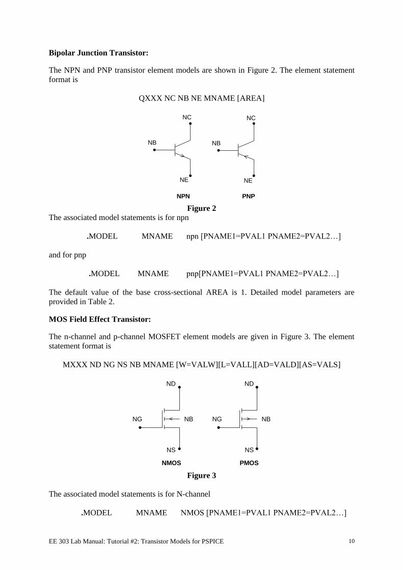
Bipolar Junction Transistor:
The NPN and PNP transistor element models are shown in Figure 2. The element statement
format is
QXXX NC NB NE MNAME [AREA]
NC
NB
NE
NC
NB
NE
NPN PNP
Figure 2
The associated model statements is for npn
.MODEL MNAME npn [PNAME1=PVAL1 PNAME2=PVAL2…]
and for pnp
.MODEL MNAME pnp[PNAME1=PVAL1 PNAME2=PVAL2…]
The default value of the base cross-sectional AREA is 1. Detailed model parameters are
provided in Table 2.
MOS Field Effect Transistor:
The n-channel and p-channel MOSFET element models are given in Figure 3. The element
statement format is
MXXX ND NG NS NB MNAME [W=VALW][L=VALL][AD=VALD][AS=VALS]
NB
ND
NG
NS
NMOS
ND
NG
NS
NB
PMOS
Figure 3
The associated model statements is for N-channel
.MODEL MNAME NMOS [PNAME1=PVAL1 PNAME2=PVAL2…]
EE 303 Lab Manual: Tutorial #2: Transistor Models for PSPICE 11
and for P-channel
.MODEL MNAME PMOS[PNAME1=PVAL1 PNAME2=PVAL2…]
The default values for the gate length, VALL, and the gate width, VALW, are 1cm.
Obviously, these are not realistic values; however, the model uses the ratio of VALL and
VALW rather than the individual values in its calculations. The drain and source areas are
VALD and VALS respectively, and the default values are 10-6
cm2. Detailed model
parameters are provided in Table 3.
Examples:
1. The input file of the circuit of Figure 4 is:
Figure 4 spice file
vsig 1 0 ac 1 sin(0 5m 100k)
VDD 6 0 DC 5V
Rsig 1 2 1K
C1 2 3 0.15uF
.op
Mamp 4 3 5 5 M2N4351 W=100U L=100U
.MODEL M2N4351 NMOS (LEVEL=1
VTO=2.1 KP=1.12M GAMMA=2.6
+ PHI=.75 LAMBDA=2.49M RD=14 RS=14
+ IS=15F PB=.8 MJ=.46
+ CBD=7.95P CBS=9.54P CGSO=11.7N
+ CGDO=9.75N CGBO=16N)
R1 3 0 400K
R2 6 3 100K
RS 5 0 1.3K
Cs 5 0 10uF
RD 6 4 4.3K
C2 4 7 0.15uF
Rl 7 0 100K
.ac dec 100 10 40meg
.print ac v(7)
.tran 0.01u 20u
.print tran v(7)
.END
+VDD
RD
R1
R2
RS
vsig
M
RsigC1
CS
RL
C2
+
-
vo
Figure 4

EE 303 Lab Manual: Tutorial #2: Transistor Models for PSPICE 12
2. The input file of the circuit of Figure
5 is:
Circuit 5
vsig 1 0 ac 1 sin(0 5m 100k)
VCC 6 0 DC 5V
Rsig 1 2 1K
C1 2 3 1uF
.op
Qamp 4 3 5 Q2N3904
.model Q2N3904
NPN(Is=6.734f +Xti=3 Eg=1.11
+Vaf=74.03 Bf=416.4 Ne=1.259
+Ise=6.734f Ikf=66.78m Xtb=1.5
+Br=.7371 Nc=2 Isc=0 Ikr=0
+Rc=1 Cjc=3.638p Mjc=.3085
+Vjc=.75 Fc=.5 Cje=4.493p
+Mje=.2593 Vje=.75 Tr=239.5n
+Tf=301.2p Itf=.4 Vtf=4 Xtf=2
+Rb=10)
R1 3 0 400K
R2 6 3 100K
RS 5 0 1.3K
Cs 5 0 10uF
RD 6 4 4.3K
C2 4 7 0.15uF
Rl 7 0 100K
.ac dec 100 10 40meg
.print ac v(7)
.tran 0.01u 20u
.print tran v(7)
.END
Vout
RC
RL
Vs
C2RB1
RB2
RECE
C1
30k
10k
4.3k
1.3k
47
100k
1
1
Q1
5V
+
-
Vcc
RS 1k
Figure 5

EE 303 Lab Manual: Tutorial #2: Transistor Models for PSPICE 13
Assignment:
A. Consider the BJT amplifier circuit shown in Figure 6 and perform the following:
1. Hand calculation to find the medium frequency gain and the upper and lower 3dB
points. Assume vs = 10mV, βF = 100, Cπ = 1pF, Cµ = 3pF.
2. Using the default parameters of the BJT, write a SPICE program to plot the gain-
frequency characteristic. From the SPICE output file, calculate the medium frequency
gain and the upper and lower 3dB points.
3. Repeat step 2 using βF = 100, IS = 10-15
, rb = 100Ω, VA = 150V, Cπ = 1pF, Cµ = 3pF
and τF = 0.2ns.
4. Compare between the results obtained using hand calculations and SPICE
simulations.
5. Comment on your results.
Vout
RC
RL
Vs
C2R
B1
RB2
RE C
E
C1
220k
220k
2.2k
1k
100
4.7k
2.2
10
Q1
6V
+
-
Vcc
RS
600W
Figure 6

EE 303 Lab Manual: Tutorial #2: Transistor Models for PSPICE 14
B. Consider the NMOS amplifier shown in Figure 7.
Use hand calculations to find the DC operating point and voltage gain.
Use Pspice default model and simulate the circuit.
Use the following NMOS parameters and simulate the circuit again.
For NMOS:
.MODEL MN NMOS LEVEL=2 LD=0.15U TOX=200.0E-10
+ MSUB=5.36726E+15 VTO=0.743469 KP=8.00059E-05 GAMMA=0.543
+ PHI=0.6 U0=655.881 UEXP=0.157282 UCRIT=31443.8
+ DELTA=2.39824 VMAX=55260.9 XJ=0.25U LAMBDA=0.0367072
+ NFS=1E+12 NEFF=1.001 NSS=1E+11 TPG=1.0 RSH=70.00
+ CGDO=4.3E-10 CGSO=4.3E-10 CJ=0.0003 MJ=0.6585
+ CJSW=8.0E-10 MJSW=0.2402 PB=0.58
For PMOS:
.MODEL MP PMOS LEVEL=2 LD=0.15U TOX=200.0E-10
+ NSUB=4.3318E+15 VTO=-0.738861 KP=2.70E-05 GAMMA=0.58
+ PHI=0.6 U0=261.977 UEXP=0.323932 UCRIT=65719.8
+ DELTA=1.79192 VMAX=25694 XJ=0.25U LAMBDA=0.0612279
+ NFS=1E+12 NEFF=1.001 NSS=1E+11 TPG=-1.0 RSH=120.6
+ CGDO=4.3E-10 CGSO=4.3E-10 CJ=0.0005 MJ=0.5052
+ CJSW=1.349E-10 MJSW=0.2417 PB=0.64
Comment on your results.
V2
R6C3
2K 22µ
300KR4
200KR5
R8
1MEG MbreakN
M1
R1 3KC1
22µ
C2
22µ
R3 2K
12V V1
6.8R2
Figure 7

EE 303 Lab Manual: Tutorial #2: Transistor Models for PSPICE 15
TABLE 1: DETAILED DIODE MODEL PARAMETERS
D Diode
D<name><+node><-node><model name>[area]
Model Parameters Default Units
IS saturation current 1E-14 A
N emission coefficient 1
RS parasitic resistance 0 ohm
CJO zero-bias pn capacitance 0 farad
VJ pn potential 1 volt
M pn grading coefficient 0.5
FC forward-bias depletion capacitance coefficient 0.5
TT transit time 0 S
BV reverse breakdown voltage infinite volts
IBV reverse breakdown current 1E-10 A
EG bandgap voltage (barrier height) 1.11 eV
XTI IS temperature exponent 3
KF flicker noise coefficient 0
AF flicker noise exponent 1

EE 303 Lab Manual: Tutorial #2: Transistor Models for PSPICE 16
TABLE 2: DETAILED BJT MODEL PARAMETERS
Q Bipolar Transistor
Q<name><collector node><base node><emitter node><[substrate node]
<model name>[area value]
Model Parameters Default Units
IS pn saturation current lE-16 A
BF ideal maximum forward beta 100
NF forward current emission coefficient 1
VAF (VA) forward Early voltage infinite V
IKF (IK) corner for fwd beta high-cur roll off infinite A
ISE (C2) base-emitter leakage saturation current 0 A
NE base-emitter leakage emission coefficient 1.5
BR ideal maximum reverse beta 1
NR reverse current emission coefficient 1
VAR (VB) reverse Early voltage infinite V
IKR corner for rev beta hi-cur roll off infinite A
ISC (C4) base-collector leakage saturation current 0 A
NC base-collector leakage emission coefficient 2.0
RB zero-bias (maximum) base resistance 0 ohm
RBM minimum base resistance RB ohm
RE emitter ohmic resistance 0 ohm
RC collector ohmic resistance 0 ohm
CJE base-emitter zero-bias pn capacitance 0 F
VJE (PE) base-emitter built-in potential 0.75 V
MJE (ME) base-emitter pn grading factor 0.33
CJC base-collector zero-bias pn capacitance 0 F
VJC (PC) base-collector built-in potential 0.75 V
MJC (MC) base-collector pn grading factor 0.33
XCJC fraction of Cbc connected into Rb 1
CJS (CCS) collector-substrate zero-bias pn capacitance 0 F
VJS (PS) collector-substrate built-in potential 0.75
MJS (MS) collector-substrate pn grading factor 0
FC forward-bias depletion capacitor coefficient 0.5
TF ideal forward transit time 0 s
XTF transit time bias dependence coefficient 0
VTF transit time dependency on Vbc infinite V
ITF transit time dependency on Ic 0 A
PTF excess phase @ 1/ (2πTF) Hz 0 °C
TR ideal reverse transit time 0 s
EG bandgap voltage (barrier height) 1.11 eV
XTB forward and reverse beta temp coefficient 0
XTI(PT) IS temperature effect exponent 3
KF flicker noise coefficient 0
AF flicker noise exponent 1
EE 303 Lab Manual: Tutorial #2: Transistor Models for PSPICE 17
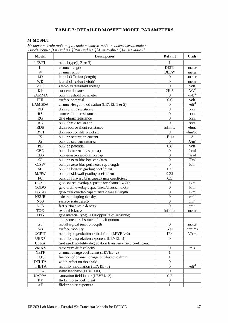
TABLE 3: DETAILED MOSFET MODEL PARAMETERS
M MOSFET
M<name><drain node><gate node><source node><bulk/substrate node>
<model name>[L=<value> ][W=<value> ][AD=<value> ][AS=<value>]
Model Description Default Units
LEVEL model type(l, 2, or 3) 1
L channel length DEFL meter
W channel width DEFW meter
LD lateral diffusion (length) 0 meter
WD lateral diffusion (width) 0 meter
VTO zero-bias threshold voltage 0 volt
KP transconductance 2E-5 A/V2
GAMMA bulk threshold parameter 0 voltl/2
PHI surface potential 0.6 volt
LAMBDA channel-length. modulation (LEVEL 1 or 2) 0 volt-1
RD drain ohmic resistance 0 ohm
RS source ohmic resistance 0 ohm
RG gate ohmic resistance 0 ohm
RB bulk ohmic resistance 0 ohm
RDS drain-source shunt resistance infinite ohms
RSH drain-source diff. sheet res. 0 ohm/sq.
IS bulk pn saturation current 1E-14 A
JS bulk pn sat. current/area 0 A/m2
PB bulk pn potential 0.8 volt
CBD bulk-drain zero-bias pn cap. 0 farad
CBS bulk-source zero-bias pn cap. 0 farad
CJ bulk pn zero-bias bot. cap./area 0 F/m2
CJSW bulk pn zero-bias perimeter cap./length 0 F/m
MJ bulk pn bottom grading coefficient 0.5
MJSW bulk pn sidewall grading coefficient 0.33
FC bulk pn forward bias capacitance coefficient 0.5
CGSO gate-source overlap capacitance/channel width 0 F/m
CGDO gate-drain overlap capacitance/channel width 0 F/m
CGBO gate-bulk overlap capacitance/channel length 0 F/m
NSUB substrate doping density 0 cm-3
NSS surface state density 0 cm-2
NFS fast surface state density 0 cm-2
TOX oxide thickness infinite meter
TPG gate material type; +1 = opposite of substrate; +1
-1 = same as substrate; 0 = aluminum
XJ metallurgical junction depth 0 meter
UO surface mobility 600 cm2/Vs
UCRIT mobility degradation critical field (LEYEL=2) IE4 V/cm
UEXP mobility degradation exponent (LEVEL=2) 0
UTRA (not used) mobility degradation transverse field coefficient
VMAX maximum drift velocity 0 m/s
NEFF channel charge coefficient (LEVEL=2) 1
XQC fraction of channel charge attributed to drain 1
DELTA width effect on threshold 0
THETA mobility modulation (LEVEL=3) 0 volt-1
ETA static feedback (LEVEL=3) 0
KAPPA saturation field factor (LEVEL=3) 0.2
KF flicker noise coefficient 0
AF flicker noise exponent 1

EE 303 Lab Manual: Experiment #1: Gain Frequency Characteristics of Single Transistor Amplifiers 18
Experiment #1: Gain Frequency Characteristics of Single Transistor
Amplifiers
Objective:
To study the effects of coupling capacitors on the gain and frequency response of single
transistor amplifiers.
Prelab work:
Students must perform the following calculations and PSPICE before coming to the lab.
1. For the circuit shown in Figure 1 perform a complete small signal ac analysis and obtain
the MF gain, the LF poles, the HF poles and bandwidth of this amplifier. Also find the
small signal input and output resistances.
2. From the results obtained in step 1, try to deduce the effect of introducing a 50F
capacitor in parallel with RE. Specifically, what is the effect of such a capacitor on the
MF gain and the bandwidth?
3. Using SPICE simulate your circuit with and without the capacitor CE and try to deduce
from the SPICE output file, the MF gain, the LF poles, the HF poles (corner frequencies)
and the bandwidth. You can also obtain the input resistance and the output resistance
using SPICE. For the SPICE analysis use the frequency range 100Hz to 8MHz. Use
β=100, Cµ=Cbc=8pF and Cπ=Cbe=30pF.
4. Tabulate the results obtained from your hand calculations and from SPICE simulation in
Table I.
You must have your SPICE output file with your hand calculations ready before you
come to the lab.
Experimental work:
1. Construct the circuit shown in Figure 1 without the capacitor CE. Apply a small ac signal
vs and make sure by monitoring the oscilloscope that the output voltage is not distorted.
Change the input frequency from 100Hz to 3MHz. At each frequency measure the small
signal voltage gain and plot it on the same graph supplied by SPICE output file.
2. Calculate the MF range, LF poles, HF poles and bandwidth from your measured gain-
frequency characteristic.
3. Insert your experimental results into Table I.
4. Compare your hand calculations, SPICE simulations and experimental measurements.
5. Repeat steps 1-4 after connecting the capacitor CE.
6. Comment on your results.

EE 303 Lab Manual: Experiment #1: Gain Frequency Characteristics of Single Transistor Amplifiers 19
Vout
RC
RL
Vs
C2R
B1
RB2
RE C
E
C1
47k
4.7k
5.6k
1k
50u
3.3k
0.5u
22u
Q1
2N3904
15V
+
-
Vcc
RS
0.5k
Table I: Summary of hand calculations, SPICE simulation and experiment
Parameter Hand
Calculation
SPICE
Simulation
Experimental
Result
MF Gain
LF Poles (Corner
Frequencies
HF Poles (Corner
Frequencies)
Bandwidth
Figure 1

EE 303 Lab Manual: Experiment #2: Gain Frequency Characteristics of Multistage Transistor Amplifiers 20
Experiment #2: Gain Frequency Characteristics of Multistage Transistor
Amplifiers
Objective:
To study the effects of coupling and junction capacitors on the gain and frequency response
of multistage transistor amplifiers.
Prelab:
Students must perform the following calculations and PSPICE before coming to the lab.
1. For the two stage amplifier circuit shown in Figure 1 perform a complete small signal ac
analysis and obtain the MF gain, the LF poles, the HF poles (corner frequencies) and
bandwidth of this multistage amplifier. Also find the small signal input and output
resistances.
2. Using SPICE simulate your circuit and try to deduce from the SPICE output file, the MF
gain, the LF poles, the HF poles and the bandwidth. Also obtain the input resistance and
the output resistance using SPICE. For the SPICE analysis use the frequency range 100Hz
to 8MHz. Use β=100, Cµ=Cbc=8pF and Cπ=Cbe=30pF.
3. Tabulate the results obtained from your hand calculations and from SPICE simulation in
Table I.
You must have your SPICE output file with your hand calculations ready before you
come to the lab.
Experimental Work:
1. Construct the circuit shown in Figure 1. Apply a small ac signal vs and make sure by
monitoring the output on oscilloscope that the output voltage is not distorted. Change the
input frequency from 100Hz to 3MHz. At each frequency measure the small signal
voltage gain and plot it on the same graph supplied by SPICE output file.
2. Calculate the MF range, LF poles, HF poles and bandwidth from your measured gain-
frequency characteristic.
3. Insert your experimental results into Table I.
4. Compare your hand calculations, SPICE simulations and experimental measurements.
5. Comment on your results.

EE 303 Lab Manual: Experiment #2: Gain Frequency Characteristics of Multistage Transistor Amplifiers 21
RB1 30k
RB2
3.3k
RC
1.8k
RE1
240
C1
1u
C2
1u
RS
0.5kV
S
220k
1.2k RL
600
1uQ1Q2
2N3904
2N3904
RE2
C3
RB3
VCC
=12V
Vout
Table I: Summary of hand calculations, SPICE simulation and experiment
Parameter Hand
Calculation
SPICE
Simulation
Experimental
Result
MF Gain
LF Poles (Corner
Frequencies
HF Poles (Corner
Frequencies)
Bandwidth
Figure 1

EE 303 Lab Manual: Experiment #3: Linear Applications of Operational Amplifiers 22
Experiment #3: Linear Applications of Operational Amplifiers
Objective:
To investigate the different linear applications of the operational amplifier, for example
inverting multiplier, inverting summer, inverting integrator, inverting differentiator and
differential amplifier.
Prelab:
Students must perform the following calculations and PSPICE before coming to the lab.
1. For the different configurations shown in Figure 1, perform an approximate hand
calculation assuming that the operational amplifier is ideal. In each case sketch the
expected output waveform.
2. Using SPICE simulate the different configurations and submit the output waveforms for
each case. For the SPICE simulation there are two ways for simulating the operational
amplifier. In the first, the op-amp is simulated using the simplified model of Figure 2
which consists of an input resistance and a voltage controlled voltage source. This
simplified model for the op-amp is fairly good at this stage. At this point it may be useful
to introduce to you the concept of SUBCIRCUIT. In many circuits we may use more than
one op-amp. In this case we have to replace each op-amp by its equivalent circuit. This
may require a long input file if we have a large number of op-amps in our circuit
especially if the op-amp is modeled using more sophisticated models than the one shown
in Figure 2. One way to avoid this is to use the concept of SUBCIRCUIT in which the
model of the op-amp is written only once and then recalled whenever necessary. The
format of the first line of a subcircuit definition is
.SUBCKT SUBNAME N1 N2 N3 …….
………..
………..
.ENDS
where SUBNAME is the name given to the SUBCIRCUIT and N1, N2, N3, .... are the
nodes to which the SUBCIRCUIT will be connected. The .ENDS control line should not
be confused with the last control line of the entire input file, .END. In a SPICE input file
with three SUBCIRCUITS, there would be three .ENDS control lines (one for each
SUBCIRCUIT) and only one .END control line.

EE 303 Lab Manual: Experiment #3: Linear Applications of Operational Amplifiers 23
CIRCUIT Hand
Calculation
SPICE
Simulation
Experimental
Result
-15V
-
+
2
3
7
4
6
+15V
741
1k, 10k, 100k
1k
Vout
-15V
-
+
2
3
7
4
6
+15V
741
10k
1k
Vout
1k
-15V
-
+
2
3
7
4
6
+15V
741
100k
Vout
1500pF
-15V
-
+
2
3
7
4
6
+15V
741
Vout
1500pF
10k
-15V
-
+
2
3
7
4
6
+15V
741
10k
1k
Vout
1k
10k
Figure 1

EE 303 Lab Manual: Experiment #3: Linear Applications of Operational Amplifiers 24
-+
Vin
1Meg
+
-10
20
5x10⁴Vin
30
Example
.SUBCKT OPAMP 20 10 30
RIN 20 10 1MEG
EOUT 30 0 20 10 5E4
.ENDS
For the Spice simulations take the input voltages of the order of 1V amplitude and 1kHz
frequency. Also you may connect a resistance of 50Ω at the output.
A SUBCIRCUIT may be called as follows:
X……. NA NB NC … SUBNAME
NA, NB, NC, … corresponds to N1, N2, N3, … but are not necessarily the same. For
example a call for the subcircuit of the above example can be:
XOP1 2 3 6 OPAMP
where 2 is the positive input of our op-amp named OP1, 3 is negative input and 6 is its
output.
You must have your SPICE output file with your hand calculations ready before you
come to the lab.
Experimental Work:
1. Construct the circuits shown in Figure 1. Apply the appropriate voltage in each case with
amplitudes of the order of 1V and frequencies of the order of 1kHz. In each case measure
the output waveform by the oscilloscope and sketch it in the table of Figure 1.
2. Compare your hand calculations, SPICE simulations and experimental results.
3. Comment on your results.
Figure 2
EE 303 Lab Manual: Experiment #4: Determination of Operational Amplifier Characteristics 25
Experiment #4: Determination of Operational Amplifier Characteristics
It is well known that the characteristics of commercially available operational amplifiers are
different from the ideal characteristics. Although it is possible to use some of these non ideal
characteristics to advantage; for example the finite bandwidth and the finite gain
characteristic can be used to construct capacitor less filters and oscillators, in general the non
ideal characteristics of the operational amplifiers may degrade the circuit performance.
Therefore, manufacturers usually provide users with the most important parameters of the
operational amplifiers. Table I shows the typical performance of selected operational
amplifiers. These data, however give the average performance of a selected type. The actual
performance of a particular operational amplifier may be different from its typical
characteristic. It is, therefore, important to know how to measure the operational amplifier
characteristics using simple equipments available in any laboratory.
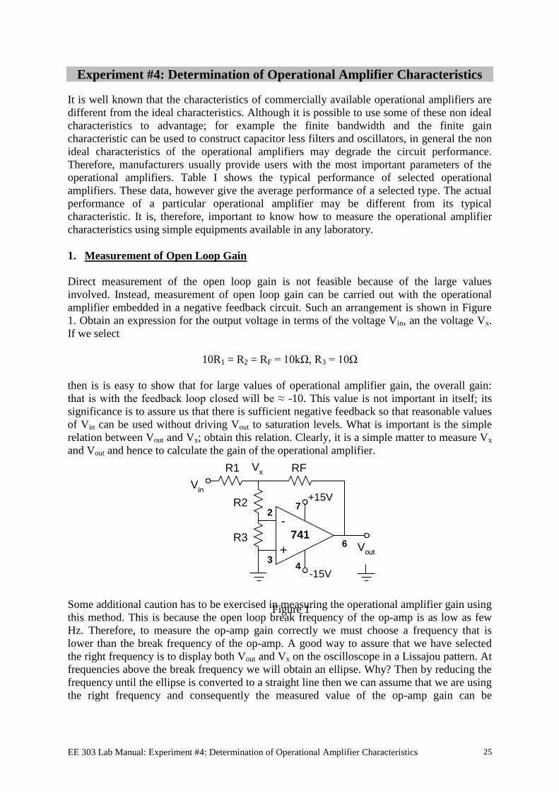
1. Measurement of Open Loop Gain
Direct measurement of the open loop gain is not feasible because of the large values
involved. Instead, measurement of open loop gain can be carried out with the operational
amplifier embedded in a negative feedback circuit. Such an arrangement is shown in Figure
1. Obtain an expression for the output voltage in terms of the voltage Vin, an the voltage Vx.
If we select
10R1 = R2 = RF = 10kΩ, R3 = 10Ω
then is is easy to show that for large values of operational amplifier gain, the overall gain:
that is with the feedback loop closed will be ≈ -10. This value is not important in itself; its
significance is to assure us that there is sufficient negative feedback so that reasonable values
of Vin can be used without driving Vout to saturation levels. What is important is the simple
relation between Vout and Vx; obtain this relation. Clearly, it is a simple matter to measure Vx
and Vout and hence to calculate the gain of the operational amplifier.
-15V
-
+
2
3
7
4
6
+15V
741
RF
Vout
R1
R2
R3
Vin
Vx
Some additional caution has to be exercised in measuring the operational amplifier gain using
this method. This is because the open loop break frequency of the op-amp is as low as few
Hz. Therefore, to measure the op-amp gain correctly we must choose a frequency that is
lower than the break frequency of the op-amp. A good way to assure that we have selected
the right frequency is to display both Vout and Vx on the oscilloscope in a Lissajou pattern. At
frequencies above the break frequency we will obtain an ellipse. Why? Then by reducing the
frequency until the ellipse is converted to a straight line then we can assume that we are using
the right frequency and consequently the measured value of the op-amp gain can be
Figure 1

EE 303 Lab Manual: Experiment #4: Determination of Operational Amplifier Characteristics 26
considered correct. Explain this. You may face some difficulties in deciding whether you are
seeing a straight line or not on the oscilloscope. Why? Anyway, try to avoid this.
2. Measurement of open loop break frequency
Consider the circuit shown in Figure 2. We know that at relatively high frequencies (w.r.t. the
open loop break frequency), the gain of the op amp can be expressed by
o
o
wjw
AA
/1
At the frequency wt corresponding to unity gain, it is easy to show that
oto wwA /
The above equation can be easily proved since we know that wt>>wo. Therefore the gain of
the op-amp can be expressed by
to
o
wwjA
AA
/1
It is easy to show that when R1 = R2 the gain Vout/Vin will be
AAVF
/21
1
-
Substituting the value of A and since Ao is very large it is easy to show that
t
VFww
A/21
1
-
From the last equation it is obvious that the gain will drop to 2/1 when wm=wt/2. We can
measure wm. Since we know the open loop voltage gain Ao, then it is easy to calculate wo.
-15V
-
+
2
3
7
4
6
+15V
741
R2
R1
Vout
Vin
3. Input offset voltage, Bias current, Offset current
In order to measure offset voltage (Vos), I1 and I2 of general purpose op-amps using
inexpensive methods, the circuits shown in Figure 3 are proposed. Verify the usefulness of
these circuits by obtaining expressions for the output voltage for each circuit. Show how the
offset parameters can be deduced from the measurement of the output voltages.
Figure 2

EE 303 Lab Manual: Experiment #4: Determination of Operational Amplifier Characteristics 27
-15V
-
+
2
3
7
4
6
+15V
741
5k
50 ohms
Vout
50 ohms
(a) Circuit to measure offset voltage; effect of
IOS is minimised
-15V
-
+
2
3
7
4
6
+15V
741
1Meg
Vout
(b) Circuit to measure bias current in
inverting terminal. Donot neglect VOS
-15V
-
+
2
3
7
4
6
+15V
741
Vout
1Meg
(c) Circuit to measure bias current in non-inverting terminal. Donot neglet VOS.
4. Slew rate and full power bandwidth
From the discussion of section 2, we found that wt=woAo. Therefore, if we consider the
circuit of Figure 2, its gain can be expressed as
ARR
RR
V
V
in
out
/)/1(1
/
12
12
-
Therefore, substituting for A=wt/s the gain can be expressed as
tin
out
wsRR
RR
V
V
/)/1(1
/
12
12
-
which corresponds to an amplifier with dc gain of –R2/R1 and a 3dB corner frequency of
wt/(1+R2/R1). Therefore, if we measure the frequency response of a closed loop amplifier
with a gain of, say, 10, the 3dB frequency of wt/11 would be achieved. This is true only if the
output voltage is quite small (less than a volt). On the other hand, op-amps are capable of
providing output signal swings that approach the voltages of the power supplies used.
(Typical values are ±10V for ±15V power supplies). The large signal frequency response of
op-amps is limited by the slew rate. Specifically, there is an upper limit for the rate of change
of the output voltage with time. This upper limit is called slew rate. This slew rate limiting
Figure 3

EE 303 Lab Manual: Experiment #4: Determination of Operational Amplifier Characteristics 28
causes distortion in large signal output sine waves. Specifically, as the frequency of the sine
wave is increased, its slope, which is highest at the zero crossings, increases until that slope
equals the op-amp slew rate. Increasing the frequency further will obviously result in a
distorted output. The op-amp data sheets usually specify the frequency at which a sine wave
output, whose peak amplitude is equal to the maximum rated voltage, starts to show
distortion. This frequency is called the full power bandwidth and is denoted by fM. It is easy
to show that
max2 V
rateslewf M
where Vmax is the maximum specified output voltage of the op-amp.
To measure the slew rate and full power bandwidth, consider the circuit shown in Figure 4. If
the input voltage is a square wave of 20V p-p (here we assume that the dc supply voltage of
the op-amp is ±15V i.e. the 20V p-p represents the maximum output voltage of the op-amp)
and if we keep the frequency at, say 1kHz, then the output will be as shown in Figure 4.
Notice the effect of slew rate. The slew rate can be easily measured from the output. It is
Slew Rate = Vout/TSR
Now apply a sine wave input of 20V p-p. Keep increasing the frequency of the input sine
wave while monitoring the output until it starts to show distortion. Determine this frequency.
This is fM. Verify the relationship between fM and the slew rate.
-15V
-
+
2
3
7
4
6
+15V
741
Vout
Vin
TSR
Vout
Vin v
o
vo
Figure 4

EE 303 Lab Manual: Experiment #4: Determination of Operational Amplifier Characteristics 29
Table I: Typical Performance of Operational Amplifiers
741 LM118 AD507
Input offset voltage (mV) ≤ 5 ≤ 4 ≤ 5
Bias current (nA) ≤ 500 ≤ 250 ≤ 15
Offset current (nA) ≤ 200 ≤ 50 ≤ 15
Open loop gain (dB) 106 100 100
CMRR (dB) 80 90 100
Input resistance (MΩ) 2 5 300
Slew rate (V/µs) 0.5 ≥ 50 35
Unity gain bandwidth (MHz) 1 15 35
Full power bandwidth (kHz) 10 1000 600

EE 303 Lab Manual: Experiment #5: Active Filters 30
Experiment #5: Active Filters
Objective:
To measure the transfer functions of several active filters and to determine their corner
frequencies, or center frequency and to determine their roll-off rates from the frequency
responses.
Prelab:
Students must perform the following calculations and PSPICE before coming to the lab.
1. For the different active-filter configurations shown in Figure 1 and 2 perform an
approximate hand calculation assuming that the operational amplifiers are ideal. In each
case sketch the expected transfer function and calculate the corner frequency, or the
center frequency, the gain of the filter configuration and its pass band, or bandwidth.
2. Using SPICE, simulate the different configurations and from SPICE output file calculate
the corner frequency, or the center frequency, the gain of the filter configuration and its
pass band, or bandwidth. The second model for simulation op-amps is shown in Figure 3.
This model is more sophisticated than the first model presented in Experiment 3, as it
models the finite input resistance, the finite differential gain, the finite output resistance,
the frequency dependence of the differential gain and the limiting characteristics of the
op-amp. Figure 3 also shows an example of how to call the op-amp SUBCIRCUIT. Try to
use the SUBCIRCUIT concept in your simulation.
For the SPICE simulations take the input voltages of the order of 1V amplitude and
obtain the frequency range from your hand calculations in step 1.
You must have your SPICE output file with your hand calculations ready before you
come to the lab.
Experimental Work:
1. Construct the circuits shown in Figure 1 and 2. Apply sinusoidal input voltage with
constant amplitude, of the order of 1V, and vary the frequency within the range decided
by your hand calculations of the prelab. In each case monitor the input and output
voltages on a dual trace oscilloscope. Measure the ratio between output and input voltages
and plot your results on the same sheet obtained from SPICE output.
2. From your measurements obtain the corner frequency, or the center frequency, the gain of
the filter in the pass band and its band, or bandwidth.
3. Compare your hand calculations, SPICE simulations and experimental measurements and
tabulate them in Table I.
4. Comment on your results.

EE 303 Lab Manual: Experiment #5: Active Filters 31
-15V
-
+
2
3
7
4
6
+15V
741
10k
10kVin
Vout
R4
C2
0.1
10k
R3 10k
R1 C
1
0.1
R2
-15V
2
3 7
4
6
+15V
741
10k
Vin
Vout
R4
10k
10k
R3 10k
R1
C1
0.1
R2
-
+C
2
0.1
Figure 1
Figure 2

EE 303 Lab Manual: Experiment #5: Active Filters 32
(1)
(2)
Rin
+
-
gm
3*v
7 R0
(4)
DL1 DL2
VL2VL1
(0)
gm
1*(
v1
-v2
)R
1C
1
(3)
(0)
gm
2*v
3 R2
C2
(7)
(0)
.SUBCKT OPAMP 1 2 4
RIN 1 2 400K
GM1 3 0 1 2 200m
R1 3 0 1MEG
C1 3 0 0.0159uF
GM2 0 7 3 0 1m
R2 7 0 1K
C2 7 0 39.8pF
GM3 0 4 7 0 5m
R0 4 0 200K
DL1 4 5 DIODE
DL2 6 4 DIODE
VL1 5 0 DC 13V
VL2 0 6 DC 13V
.MODEL DIODE D
.ENDS
A SUBCKT call for an op-amp connected between points 11, 17, 30 where 11 is the positive
input, 17 is the negative input and 30 is the output is:
x….. 11 17 30 OPAMP
Figure 3. SPICE model for operational amplifier

EE 303 Lab Manual: Experiment #5: Active Filters 33
Table I: Summary of hand calculations, SPICE simulation and experiment
Circuit Hand
Calculation
SPICE
Simulation
Experimental
Result
Figure
1
MF Gain
Center
Frequency
Bandwidth
Figure
2
MF Gain
Center
Frequency
Bandwidth

EE 303 Lab Manual: Experiment #6: Feedback and Non-linear Distortion 34
Experiment #6: Feedback and Non-linear Distortion
Objective:
The major objective of this experiment is to illustrate how negative feedback can reduce
nonlinear distortion.
Introduction:
Consider the operational amplifier circuit shown in Figure 1. Because the output resistance of
the op-amp is about 50Ω then it is expected that the power delivered to the loudspeaker will
not be the maximum power. Thus if you listen to the output from the speaker using an input
of around 0.5V p-p then you will not hear a loud sound. A possible solution for this problem
is to connect an output stage between the op-amp output and the speaker, as shown in Figure
2. If you connect such a circuit you will notice that the sound is now more loud. However, it
will be distorted. There are two sources for this distortion. The first as you know is the
crossover distortion is to connect the two diodes D1 and D2 as shown in Figure 3. Now it is
expected that the crossover distortion will disappear. Unfortunately it will not disappear
completely unless the two transistors are identical and also the two diodes are identical and
that all the transistors and diodes easily satisfied if you are using discrete elements. So what
is the solution? The solution is simply apply negative feedback across the whole circuit as
shown in Figure 4.
Prelab work:
Students must perform the following calculations and PSPICE before coming to the lab.
1. Using simple hand calculation try to sketch the voltage across the speaker in all cases.
2. Using SPICE simulate the circuits of Figures 1 to 4 and in each case obtain an output file
including the output voltage across the speaker. Assume default values for the transistors
and diodes. Also assume that the input voltage is a pure sine wave with frequency 1kHz
and amplitude around 0.25V.
You must have your SPICE output file with your hand calculations ready before you
come to the lab.
Experimental work:
1. Construct the circuit in Figure 1 to 4 one by one and in each observe the output on the
oscilloscope and listen to it from the speaker. Sketch your output.
2. Compare the calculated, simulated and measured results.
3. Now rather than obtaining the input from a function generator, obtain it from the output
of a microphone. You may need to change the 10k resistance and make it 1k, this because
the output of the microphone is usually small so we need more amplification from the op-
amp. Observe the output on the oscilloscope and listen to it, in the four cases of Figure 1
to 4. In each case try to sense how clear and loud your output is. Comment on your
results.

EE 303 Lab Manual: Experiment #6: Feedback and Non-linear Distortion 35
4. Try to write a conclusion to illustrate the usefulness of negative feedback as a powerful
mean for reducing nonlinear distortion. Are there any advantages for negative feedback?
Table I: Summary of hand calculations, SPICE simulation and experiment
Output Waveforms Sound
Level
Hi or Lo Hand
Calculation SPICE Experiment
Figure 1
Figure 2
Figure 3
Figure 4

EE 303 Lab Manual: Experiment #6: Feedback and Non-linear Distortion 36
8W Speaker
-15V
-
+
2
3
7
4
6
+15V
741
100k
10k
Vin
10k
-15V
-
+
2
3
7
4
6
+15V
741
100k
10k
Vin
10k
2k
2k
BD237
BD238
+12V
-12V
8W Speaker
Figure 1
Figure 2

EE 303 Lab Manual: Experiment #6: Feedback and Non-linear Distortion 37
-15V
-
+
2
3
7
4
6
+15V
741
100k
10k
Vin
10k
2k
2k
BD237
BD238
+12V
-12V
8W Speaker1N660
1N660D2
D1
-15V
-
+
2
3
7
4
6
+15V
741
100k
10k
Vin
10k
2k
2k
BD237
BD238
+12V
-12V
8W Speaker
Figure 3
Figure 4

EE 303 Lab Manual: Experiment #7: Feedback Amplifiers 38
Experiment #7: Feedback Amplifiers
Objective:
To study the properties of negative feedback amplifiers.
Prelab work:
Students must perform the following calculations and PSPICE before coming to the lab.
1. For the circuit shown in Figure 1, use the feedback techniques to perform a complete ac
small signal analysis and obtain the MF gain, the LF poles, the HF poles, the bandwidth,
and the input resistance, the output resistance of this amplifier with and without feedback.
2. Using SPICE simulate your circuit and from SPICE output file calculate the parameters
of the amplifier obtained in step 1. For the SPICE analysis use the frequency range
100Hz to 8MHz. Use β=100, Cµ=Cbc=8pF and Cπ=Cbe=30pF.
3. Tabulate the results obtained from your hand calculations and from SPICE simulation in
Table I.
You must have your SPICE output file with your hand calculations ready before you
come to the lab.
Experimental work:
1. Construct the circuit shown in Figure 1. Apply a small ac signal vs and make sure by
monitoring the oscilloscope that the output voltage is not distorted. Change the input
frequency from 100Hz to 3MHz. At each frequency measure the small signal voltage gain
and plot it on the same graph supplied by SPICE output file.
2. Calculate the MF range, LF poles, HF poles and bandwidth from your measured gain-
frequency characteristic.
3. Measure Rin and Rout at medium frequency and tabulate the results of steps 1, 2 and 3 in
Table I.
4. Now remove the resistor RF and capacitor CF and repeat steps 1, 2 and 3.
5. Compare your hand calculations, SPICE simulations and experimental measurements.
6. Comment on your results.

EE 303 Lab Manual: Experiment #7: Feedback Amplifiers 39
Vout
RC
RL
Vs
C2
RB1
RB2
C1
30k
3.3k
0.47k
3.3k
1u
1u Q1
2N3904
15V
+
-
Vcc
RS
50W
RF
100W
CF
100
Table I: Summary of hand calculations, SPICE simulation and experiment
With Feedback Without Feedback
Hand
Calculation SPICE Experiment
Hand
Calculation SPICE Experiment
MF Gain
Bandwidth
Rin
Rout
Figure 1

EE 303 Lab Manual: Experiment #8: Oscillators 40
Experiment #8: Oscillators
Objective:
To investigate the operation of sinusoidal oscillators using operational amplifiers,
specifically, the phase shift oscillator, the Wein-Bridge oscillator and the quadrature
oscillator.
Prelab work:
Students must perform the following calculations and PSPICE before coming to the lab.
1. For the different oscillator circuits shown in Figure 1, perform an approximate hand
calculation assuming ideal operational amplifiers. In each case obtain an expression for
the frequency of oscillation and the condition of oscillation.
2. Using SPICE simulate the different configurations and from SPICE output file obtain the
oscillation frequency. For simulating the op-amp you can use the first model presented in
Experiment # 3 or the second model presented in Experiment # 7. Try the second model
to see the effect of the gain frequency characteristic of the op-amp on the frequency and
condition of oscillation. For the SPICE simulation it is essential to calculate the closed
loop gain of your circuit. As you know the closed loop gain is the overall gain of the
amplifier and the feedback network. Of course in oscillator circuits, we do not have an
input ac signal. However, we can open the loop at an appropriate point and assume that an
input voltage of say, 1V ac is applied at this input. Then we calculate the output voltage
and phase angle as functions of the input frequency. If we find that at certain frequency
the overall gain is unity and the overall phase angle is zero, then this is the possible
frequency of oscillation. Notice that for oscillation to start the condition of oscillation
must be satisfied. Thus, do not be disappointed if you notice that for certain value of R1
the overall gain cannot be unity and phase shift is not zero. Try again using a larger value
of R1.
3. Tabulate the results obtained from your hand calculations and from SPICE simulation in
Table I.
You must have your SPICE output file with your hand calculations ready before you
come to the lab.
Experimental work:
1. Construct the circuit shown in Figure 1. In each case change the variable resistance until
you get an output on the oscilloscope. This means that your circuit is oscillating. In each
case record the value of the resistance R1 at which oscillation just starts to appear on the
oscilloscope. Check whether it satisfies the condition of oscillation obtained from your
theoretical work.
2. In each case observe the output waveform. Is it pure sinusoidal signal? If not, what are the
sources of distortion in your opinion?
3. Also observe the amplitude of the output waveforms. Can we control it? If the answer is
yes, how?

EE 303 Lab Manual: Experiment #8: Oscillators 41
4. Tabulate your results in Table I.
Table I: Summary of hand calculations, SPICE simulation and experiment
Circuit Hand Calculation SPICE Simulation Experimental Result
Figure 1
Frequency
Condition
of
Oscillation
Figure 2
Frequency
Condition
of
Oscillation
Figure 3
Frequency
Condition
of
Oscillation

EE 303 Lab Manual: Experiment #8: Oscillators 42
-15V
-
+
2
3
7
4
6
+15V
741
270W
Vout
R4
C2
15n10k
R3 10k
R2
R1
C1 15n
(a) Wein Bridge Oscillator
fo = 1/2πCR
C = 15nF , R = 10kΩ
R2 = 270Ω , R1 > 2R2
-15V
-
+
2
3
7
4
6
+15V
741
10k
Vout
C
15n
R2
R1
1k1k1k RR RC
15n
C
15n
(b) Phase shift Oscillator
fo = 1/2π 6 CR
C = 15nF, R = 1kΩ
R2 = 10kΩ, R1 > 29R2
-15V
-
+
2
3
7
4
6
+15V
741
5.1k
Vout1
R2
15n
-15V
-
+
2
3
7
4
6
+15V
741
5.1k
R3
C1
15n
C2
15n
C3
R1
Vout2
(c) Quadrature Oscillator
fo = 1/2π 3232 RRCC
C1=C2=C3=15nF, R = 1kΩ
R2=R3=5.1kΩ , R1 > R2
Figure 1


![Index [mediendb.hjr-verlag.de] · INDEX 303 Qualität lenken 179, 183 Qualität planen 178, 180 Qualitätskosten 185 Qualitätslenkung 179 Qualitätsmanagement 171 Qualitätsmanagementplan](https://img.pdfslide.net/doc/110x75/608dde2876bfef3914771345/index-index-303-qualitt-lenken-179-183-qualitt-planen-178-180-qualittskosten.jpg)