Embed Size (px)
Citation preview
rXXXX American Chemical Society A dx.doi.org/10.1021/ja109793s | J. Am. Chem. Soc. XXXX, XXX, 000–000
COMMUNICATION
pubs.acs.org/JACS
Large-Area Graphene Single Crystals Grown by Low-PressureChemical Vapor Deposition of Methane on CopperXuesong Li,† Carl W. Magnuson,† Archana Venugopal,‡ Rudolf M. Tromp,§ James B. Hannon,§
Eric M. Vogel,‡ Luigi Colombo,*,|| and Rodney S. Ruoff*,†
†Department of Mechanical Engineering and the Texas Materials Institute, The University of Texas at Austin,1 University Station C2200, Austin, Texas 78712-0292, United States‡Department of Electrical Engineering, The University of Texas at Dallas, Richardson, Texas 75080, United States§IBM T. J. Watson Research Center, Yorktown Heights, New York 10598, United States
)Texas Instruments, 13121 TI Boulevard, Dallas, Texas 75243, United States
ABSTRACT: Graphene single crystals with dimensions ofup to 0.5mmon a side were grown by low-pressure chemicalvapor deposition in copper-foil enclosures using methane asa precursor. Low-energy electron microscopy analysisshowed that the large graphene domains had a singlecrystallographic orientation, with an occasional domainhaving two orientations. Raman spectroscopy revealed thegraphene single crystals to be uniform monolayers with alow D-band intensity. The electron mobility of graphenefilms extracted from field-effect transistor measurementswas found to be higher than 4000 cm2 V-1 s-1 at roomtemperature.
Graphene growth by chemical vapor deposition (CVD) hasbeen receiving significant attention recently because of the
ease with which large-area films can be grown, but the growth oflarge-domain or large-grain-size single crystals has not beenreported to date.1 In our earlier work, we found that growth ofgraphene on Cu by CVD occurs predominantly by surfacenucleation followed by a two-dimensional growth process, butthe domain size was limited to a few tens of micrometers.2,3 Thepresence of domain boundaries has been found to be detrimentalto the transport properties; the precise mechanism of the degrada-tion still remains elusive, but what is known is that structuraldefects promote surface reactions with adsorbates from theambient or with deposited dielectrics.3 The presence of heptagonsand pentagons in the network of hexagons has been observedexperimentally, and first-principles quantum-transport calculationshave predicted that the periodicity-breaking disorder can adverselyaffect transport properties.4,5 Any of these defects can give rise tohigher surface chemical activity that would further disrupt the sp2-bonding nature of graphene and thus impact graphene’s funda-mental properties. Therefore, it is imperative that large singlecrystals of graphene be grown to minimize the presence of defectsarising from boundaries between misoriented domains. In thiscommunication, we report a very low pressure CVD process thatyields graphene with domains of up to 0.5 mm in size, which is afactor of ∼30 times larger than previously reported.3
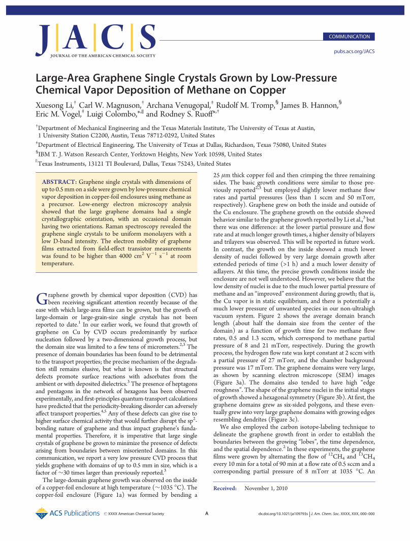
The large-domain graphene growth was observed on the insideof a copper-foil enclosure at high temperature (∼1035 �C). Thecopper-foil enclosure (Figure 1a) was formed by bending a
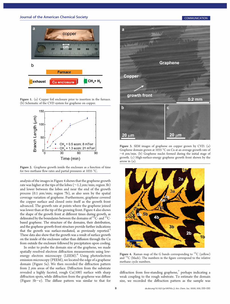
25 μm thick copper foil and then crimping the three remainingsides. The basic growth conditions were similar to those pre-viously reported2,3 but employed slightly lower methane flowrates and partial pressures (less than 1 sccm and 50 mTorr,respectively). Graphene grew on both the inside and outside ofthe Cu enclosure. The graphene growth on the outside showedbehavior similar to the graphene growth reported by Li et al.,3 butthere was one difference: at the lower partial pressure and flowrate and at much longer growth times, a higher density of bilayersand trilayers was observed. This will be reported in future work.In contrast, the growth on the inside showed a much lowerdensity of nuclei followed by very large domain growth afterextended periods of time (>1 h) and a much lower density ofadlayers. At this time, the precise growth conditions inside theenclosure are not well understood. However, we believe that thelow density of nuclei is due to the much lower partial pressure ofmethane and an “improved” environment during growth; that is,the Cu vapor is in static equilibrium, and there is potentially amuch lower pressure of unwanted species in our non-ultrahighvacuum system. Figure 2 shows the average domain branchlength (about half the domain size from the center of thedomain) as a function of growth time for two methane flowrates, 0.5 and 1.3 sccm, which correspond to methane partialpressure of 8 and 21 mTorr, respectively. During the growthprocess, the hydrogen flow rate was kept constant at 2 sccm witha partial pressure of 27 mTorr, and the chamber backgroundpressure was 17 mTorr. The graphene domains were very large,as shown by scanning electron microscope (SEM) images(Figure 3a). The domains also tended to have high “edgeroughness”. The shape of the graphene nuclei in the initial stagesof growth showed a hexagonal symmetry (Figure 3b). At first, thegraphene domains grew as six-sided polygons, and these even-tually grew into very large graphene domains with growing edgesresembling dendrites (Figure 3c).
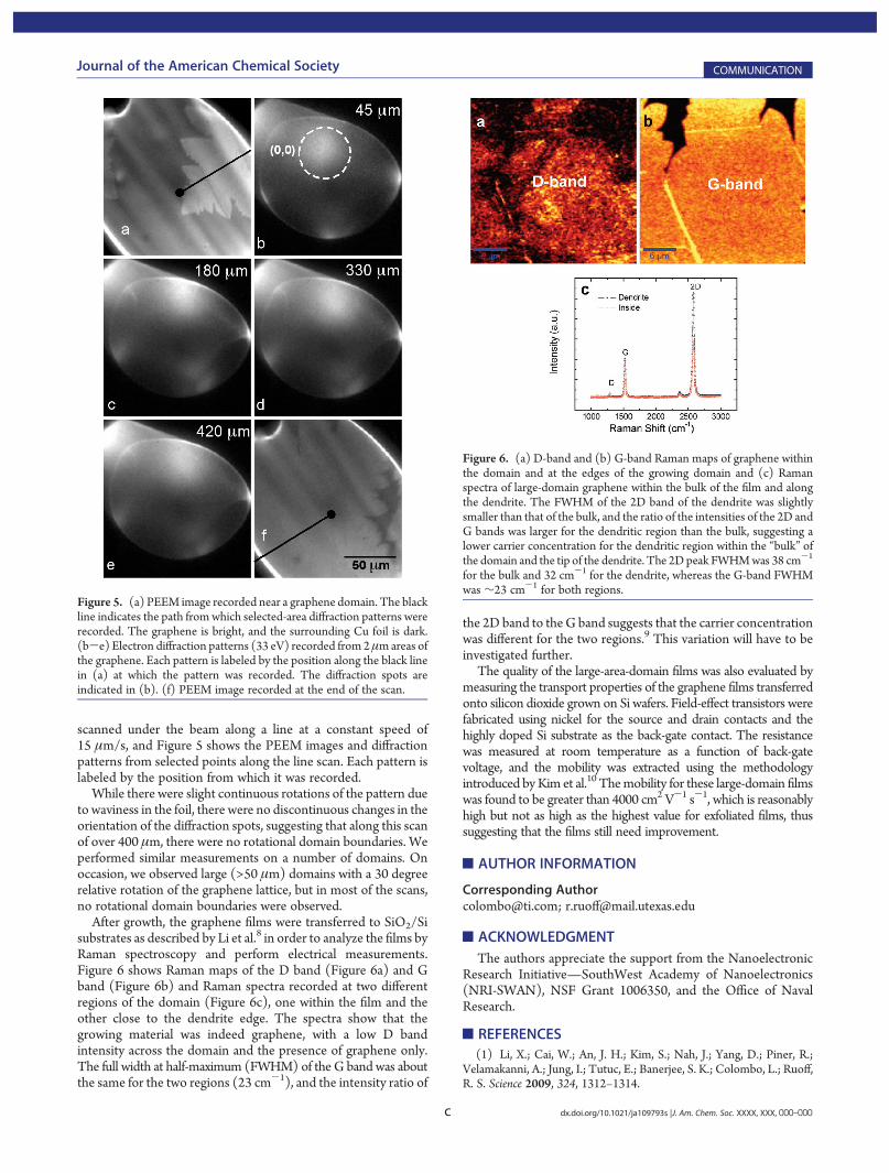
We also employed the carbon isotope-labeling technique todelineate the graphene growth front in order to establish theboundaries between the growing “lobes”, the time dependence,and the spatial dependence.2 In these experiments, the graphenefilms were grown by alternating the flow of 12CH4 and
13CH4
every 10 min for a total of 90 min at a flow rate of 0.5 sccm and acorresponding partial pressure of 8 mTorr at 1035 �C. An
Received: November 1, 2010
B dx.doi.org/10.1021/ja109793s |J. Am. Chem. Soc. XXXX, XXX, 000–000
Journal of the American Chemical Society COMMUNICATION
analysis of the images in Figure 4 shows that the graphene growthrate was higher at the tips of the lobes (∼1.2 μm/min; region 3b)and lower between the lobes and near the end of the growthprocess (0.1 μm/min; region 7b), as also seen by the spatialcoverage variation of graphene. Furthermore, graphene coveredthe copper surface and closed onto itself as the growth frontadvanced. The growth rate at points where the graphene joinedwas lower than at the tip of the growing front. Figure 4 also showsthe shape of the growth front at different times during growth, asdelineated by the boundaries between the domains of 12C- and 13C-based graphene. The structure of the domains, their distribution,and the graphene growth-front structure provide further indicationsthat the growth was surface-mediated, as previously reported.2
These data also show that the growth was a result of surface growthon the inside of the enclosure rather than diffusion through the Cufrom outside the enclosure followed by precipitation upon cooling.
In order to probe the domain size of the graphene, we madespatially resolved electron diffraction measurements using low-energy electron microscopy (LEEM).6 Using photoelectronemissionmicroscopy (PEEM), we located the edge of a graphenedomain (Figure 5a). We then recorded the diffraction patternfrom 2 μm areas of the surface. Diffraction from the substraterevealed a highly faceted, rough Cu(100) surface with sharpdiffraction spots, while diffraction from the graphene was diffuse(Figure 5b-e). The diffuse pattern was similar to that for
diffraction from free-standing graphene,7 perhaps indicating aweak coupling to the rough substrate. To estimate the domainsize, we recorded the diffraction pattern as the sample was
Figure 1. (a) Copper foil enclosure prior to insertion in the furnace.(b) Schematic of the CVD system for graphene on copper.
Figure 2. Graphene growth inside the enclosure as a function of timefor two methane flow rates and partial pressures at 1035 �C.
Figure 3. SEM images of graphene on copper grown by CVD. (a)Graphene domain grown at 1035 �C on Cu at an average growth rate of∼6 μm/min. (b) Graphene nuclei formed during the initial stage ofgrowth. (c) High-surface-energy graphene growth front shown by thearrow in (a).
Figure 4. Raman map of the G bands corresponding to 12C (yellow)and 13C (black). The numbers in the figure correspond to the relativemethane cycle numbers.
C dx.doi.org/10.1021/ja109793s |J. Am. Chem. Soc. XXXX, XXX, 000–000
Journal of the American Chemical Society COMMUNICATION
scanned under the beam along a line at a constant speed of15 μm/s, and Figure 5 shows the PEEM images and diffractionpatterns from selected points along the line scan. Each pattern islabeled by the position from which it was recorded.
While there were slight continuous rotations of the pattern dueto waviness in the foil, there were no discontinuous changes in theorientation of the diffraction spots, suggesting that along this scanof over 400 μm, there were no rotational domain boundaries. Weperformed similar measurements on a number of domains. Onoccasion, we observed large (>50 μm) domains with a 30 degreerelative rotation of the graphene lattice, but in most of the scans,no rotational domain boundaries were observed.
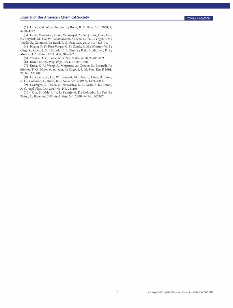
After growth, the graphene films were transferred to SiO2/Sisubstrates as described by Li et al.8 in order to analyze the films byRaman spectroscopy and perform electrical measurements.Figure 6 shows Raman maps of the D band (Figure 6a) and Gband (Figure 6b) and Raman spectra recorded at two differentregions of the domain (Figure 6c), one within the film and theother close to the dendrite edge. The spectra show that thegrowing material was indeed graphene, with a low D bandintensity across the domain and the presence of graphene only.The full width at half-maximum (FWHM) of the G band was aboutthe same for the two regions (23 cm-1), and the intensity ratio of
the 2D band to theG band suggests that the carrier concentrationwas different for the two regions.9 This variation will have to beinvestigated further.
The quality of the large-area-domain films was also evaluated bymeasuring the transport properties of the graphene films transferredonto silicon dioxide grown on Si wafers. Field-effect transistors werefabricated using nickel for the source and drain contacts and thehighly doped Si substrate as the back-gate contact. The resistancewas measured at room temperature as a function of back-gatevoltage, and the mobility was extracted using the methodologyintroduced by Kim et al.10 Themobility for these large-domain filmswas found to be greater than 4000 cm2 V-1 s-1, which is reasonablyhigh but not as high as the highest value for exfoliated films, thussuggesting that the films still need improvement.
’AUTHOR INFORMATION
Corresponding [email protected]; [email protected]
’ACKNOWLEDGMENT
The authors appreciate the support from the NanoelectronicResearch Initiative—SouthWest Academy of Nanoelectronics(NRI-SWAN), NSF Grant 1006350, and the Office of NavalResearch.
’REFERENCES
(1) Li, X.; Cai, W.; An, J. H.; Kim, S.; Nah, J.; Yang, D.; Piner, R.;Velamakanni, A.; Jung, I.; Tutuc, E.; Banerjee, S. K.; Colombo, L.; Ruoff,R. S. Science 2009, 324, 1312–1314.
Figure 5. (a) PEEM image recorded near a graphene domain. The blackline indicates the path fromwhich selected-area diffraction patterns wererecorded. The graphene is bright, and the surrounding Cu foil is dark.(b-e) Electron diffraction patterns (33 eV) recorded from 2μmareas ofthe graphene. Each pattern is labeled by the position along the black linein (a) at which the pattern was recorded. The diffraction spots areindicated in (b). (f) PEEM image recorded at the end of the scan.
Figure 6. (a) D-band and (b) G-band Raman maps of graphene withinthe domain and at the edges of the growing domain and (c) Ramanspectra of large-domain graphene within the bulk of the film and alongthe dendrite. The FWHM of the 2D band of the dendrite was slightlysmaller than that of the bulk, and the ratio of the intensities of the 2D andG bands was larger for the dendritic region than the bulk, suggesting alower carrier concentration for the dendritic region within the “bulk” ofthe domain and the tip of the dendrite. The 2Dpeak FWHMwas 38 cm-1
for the bulk and 32 cm-1 for the dendrite, whereas the G-band FWHMwas ∼23 cm-1 for both regions.
D dx.doi.org/10.1021/ja109793s |J. Am. Chem. Soc. XXXX, XXX, 000–000
Journal of the American Chemical Society COMMUNICATION
(2) Li, X.; Cai, W.; Colombo, L.; Ruoff, R. S. Nano Lett. 2009, 9,4268–4272.(3) Li, X.; Magnuson, C. W.; Venugopal, A.; An, J.; Suk, J. W.; Han,
B.; Borysiak, M.; Cai, W.; Velamakanni, A.; Zhu, Y.; Fu, L.; Vogel, E. M.;Voelkl, E.; Colombo, L.; Ruoff, R. S. Nano Lett. 2010, 10, 4328–34.(4) Huang, P. Y.; Ruiz-Vargas, C. S.; Zande, A. M.; Whitney, W. S.;
Garg, S.; Alden, J. S.; Hustedt, C. J.; Zhu, Y.; Park, J.; McEuen, P. L.;Muller, D. A. Nature 2011, 469, 389–392.(5) Yazyev, O. V.; Louie, S. G. Nat. Mater. 2010, 9, 806–809.(6) Bauer, E. Rep. Prog. Phys. 1994, 57, 895–938.(7) Knox, K. R.; Wang, S.; Morgante, A.; Cvetko, D.; Locatelli, A.;
Mentes, T. O.; Nino, M. A.; Kim, P.; Osgood, R. M. Phys. Rev. B 2008,78, No. 201408.(8) Li, X.; Zhu, Y.; Cai, W.; Borysiak, M.; Han, B.; Chen, D.; Piner,
R. D.; Colombo, L.; Ruoff, R. S. Nano Lett. 2009, 9, 4359–4363.(9) Casiraghi, C.; Pisana, S.; Novoselov, K. S.; Geim, A. K.; Ferrari,
A. C. Appl. Phys. Lett. 2007, 91, No. 233108.(10) Kim, S.; Nah, J.; Jo, I.; Shahrjerdi, D.; Colombo, L.; Yao, Z.;
Tutuc, E.; Banerjee, S. K. Appl. Phys. Lett. 2009, 94, No. 062107.


![Epitaxial Ultrathin Organic Crystals on Graphene for High ... · taxy of ultrathin organic crystals on graphene and boron nitride (BN) for electronic device applications.[13,14] The](https://img.pdfslide.net/doc/110x75/5fdb7aabcacd653b0d17fb50/epitaxial-ultrathin-organic-crystals-on-graphene-for-high-taxy-of-ultrathin.jpg)