Embed Size (px)
Citation preview
1
Large area in situ fabrication of Poly(pyrrole)-
nanowires on flexible thermoplastic films using
Nanocontact printing
Alvaro GARCIA-CRUZ1*, Michael LEE1, Pedro MAROTE, Nadia ZINE1, Monique SIGAUD1,
Anne BONHOMME1, Raquel PRUNA2, Manuel LOPEZ2, Joan BAUSELLS3, Nicole
JAFFREZIC1, and Abdelhamid ERRACHID1**
11nstitut des Sciences Analytiques (ISA), Université Claude Bernard Lyon, 5 rue de la Doua
69100 Villeurbanne cedex, France.
2Departament d'Electrònica, Universidad Autónoma de Barcelona, 08193, Bellaterra, Spain.
3Centro Nacional de Microelectrónica, Universidad Autónoma de Barcelona, 08193 Bellaterra,
Spain.
E-mail:*[email protected]; **[email protected].
Abstract: Highly efficient nano-engineering tools will certainly revolutionize the
biomedical and sensing devices research and development in the years to come. Here, we present
a novel high performance conducting poly(pyrrole) nanowires (PPy-NW) patterning technology
on thermoplastic surfaces (poly(ethylene terephthalate (PETE), poly(ethylene 2,6-naphthalate
(PEN), polyimide (PI), and cyclic olefin copolymer (COC)) using nanocontact printing and
controlled chemical polymerization (nCP-CCP) technique. The technique uses a commercial
compact disk (CD) as a template to produce nanopatterned polydimethylsiloxane (PDMS)
stamps. The PDMS nanopatterned stamp was applied to print the PPy-NWs and the developed
technology of nCP-CCP produced 3D conducting nanostructures. This new and very promising
nanopatterning technology was achieved in a single step and with a low cost of fabrication over
large areas.
Keywords: Nanocontact printing, Poly(pyrrole), thermoplastic films, silane chemistry.
1. Introduction
In the last few years, there has been a growing global interest in research and
development of nanomaterials. Nanostructures present a large surface area-to-volume ratio and
they obtain unique and very specific electrical properties. Therefore, sensing devices based on
nanomaterials result in high sensitivity and the rise of conductivity [1,2]. So far, there is a vast
diversity of systems that have been explored, for e.g., semiconductor single-walled carbon
nanotubes (SWCNTs) [3,4,5,6], silicon nanowires (SiNWs) [7], tin dioxide (SnO2) nanowires
[8], indium (III) oxide (In2O3) nanowires [9], etc. However, the current synthetic methods are
Page 1 of 22 AUTHOR SUBMITTED MANUSCRIPT - MRX-102506.R1
123456789101112131415161718192021222324252627282930313233343536373839404142434445464748495051525354555657585960
2
unable to selectively grow and manipulate nanostructures, typically CNTs [10] and SiNWs [11].
Therefore, and by consequence, the fabrication technique requires complex post-synthesis steps
using sophisticated manipulating tools [12]. Furthermore, functionalization can only be
performed as post-assembly processes [13]. The most common manipulation technique include
atomic force microscopy (AFM) [14], random dispersion suspended onto pre-patterned
electrodes [15], and lithographically patterning catalysts on electrodes [16]. Nevertheless, all of
these techniques, have low throughput, restricted controllability, and consequently are
unattractive for large scale fabrication processes.
Contrary to the restrictions of the previously mentioned nanomaterials, conducting
polymers (CP) due to their simple fabrication and easy manipulation are emerging as a promising
material for the synthesis of nanostructured materials and devices. CP-NWs have been
intensively studied, because of their extraordinary properties and their potential for commercial
applications [17]. Polypyrrole nanowires (PPy-NWs) have excellent magnetic, optical, and
tuneable electrical properties [18,19]. Besides, their biocompatibility [20] and flexible
electrochemical or chemical synthesis routes, they offer several advantages over others
nanostructures [21]. The first methods to synthesize PPy-NWs used electronic microscopy,
photolithography, and electrochemical techniques, for e.g. (via dip-pen lithography and
electrochemical polymerization) [22,23]. A common fabrication technique of PPy-NWs based
devices was carried out by electrochemical polymerization in nanochannels between
microfabricated gold electrodes [24] fashioned by e-beam lithography [25]. These techniques
allow position control and shape, however, they are known to be time-consuming and costly.
Today, synthetic methods of CP-NWs include: scanning probe lithography [26],
mechanical stretching [27], electrospinning [28], template electrochemical [29,30,31] and
wetting procedures [32]. Recent improvements in the fabrication of PPy-NWs on polymeric
surfaces have been researched [33] by soft techniques. PPy-NWs have been fabricated on
poly(methyl methacrylate) (PMMA) by creating covalent bonds between the CP film and
moieties of the polymer substrate. This has been made possible by employing silane derivatives,
for e.g., N-(3-trimethoxysilyl-propyl) pyrrole (Py-silane) [34]. Several surface coupling reagents
(linkers) have been used such as silanes, thiols, and surfactants [35] to improve the adhesion of
PPy-NWs to the substrate. Similar approaches use oppositely charged CPs on charged self-
assembled monolayers (SAMs) [36]. Therefore, and to conclude, the fabrication methods of PPy-
NWs are still time-consuming, complex, and costly.
The aim of this work is to overcome these problems and present an easy and cost efficient
way of fabricating PPy-NWs. Microcontact printing (µCP) technique has become an easy tool
for nanopatterning. We have previously proposed alternative techniques for micro- and
nanopatterning on conductive substrates that allows us to print thiol nanolines [37] and PPy
microrings on gold substrates [38]. Besides, PPy microrings were fabricated by combining thiol
patterning on gold surfaces and electropolymerization of Pyrrole. Furthermore, we have recently
introduced an innovative PPy micropatterning technique by µCP and chemical polymerization
[39] based on nonconductive substrates (glass and PETE). Finally, the printed PPy micropatterns
were functionalized with antibodies for fluorescent recognition. Finally, this technology has been
used to produce PPy microwires (PPyµW) and to fabricate immunosensors [40].
Page 2 of 22AUTHOR SUBMITTED MANUSCRIPT - MRX-102506.R1
123456789101112131415161718192021222324252627282930313233343536373839404142434445464748495051525354555657585960

3
Here, we present a new revolutionizing printing technology based in silane chemistry,
which has allowed us to pattern PPy on nonconductive and conductive substrates at the
nanoscale. The nanopatterned PDMS stamps can produce a high quality printing of PPy-NWs
and this technique has been used before within our group for nCP of thiols [41,42,43].
Consequently, we describe a simple process to fabricate PPy-NWs supported on thermoplastics
films via nanocontact printing techniques combined with controlled catalytic polymerization
(nCP-CCP). The nCP-CCP technique offers the printing of PPy-NWs in-situ and at the desired
position. To be more precise, our printing technique was tested on different surfaces:
poly(ethylene terephthalate (PETE), poly(ethylene 2,6-naphthalate (PEN), polyimide (PI), and
cyclic olefin copolymer (COC). We have also studied the printing process and the surface
properties to understand the different physical and mechanical characteristics of the PPy patterns
(contact angle measurements (CAM), Atomic Force Microscopy (SEM), scanning electron
microscopy (SEM), attenuated total reflectance-Fourier transform infrared spectroscopy (ATR-
FTIR), X-ray photoelectron spectroscopy (XPS), and electrochemical impedance spectroscopy
(EIS)). The innovative technique can be a breakthrough for printing over large areas and easy
fabrication of sub micrometer conducting polymeric patterns that would be advantageous in
electronics, microchips, lab on chip, biosensors, etc.
2. Experimental part
2.1 Methods, chemicals, and techniques
Chemicals and Reagents: Sulfuric acid (H2SO4, 30 wt. % in H2O), glutaraldehyde (GA),
phosphate buffered saline (PBS), sodium dodecyl sulfate (SDS), iron (III) chloride, Pyrrole, 1-
Ethyl-3-(3-dimethylaminopropyl) carbodiimide hydrochloride (EDC), N-hydroxysuccinimide
(NHS), silver nitrate (Ag(NO3)), iron (III) chloride (FeCl3), and Lithium chloride (LiCl) were
purchased from Sigma Aldrich, France. 11-(triethoxysilyl)undecanal (TESUD) was purchased
from Gelest, USA. N-(3-trimethoxysilyl-propyl) pyrrole (Py-silane) was purchased from ABCR
GmbH & Co. KG, Germany. Finally, hydrogen peroxide (H2O2) (35 % wt.) and potassium
hydroxide (KOH) were obtained from Acros Organics, France.
Polymers: PDMS (Sylgard 184) was purchased from Dow Corning, France. The applied
thermoplastic films were PI (HN, 125 µm, DuPont), PETE (125 µ m, Goodfellow), PEN (125 µ
m, Goodfellow), and COC (188 µ m, ChipShop, Germany).
Microcontact printer: Semi-automatic Micro-Contact-Printing System µ-CP 3.0 from GeSiM
Gesellschaft fuer Silizium-Mikrosysteme mbH.
Microscopy: Scanning electron microscope (SEM) images were obtained with a Hitachi SEM
S800, France. Atomic force microscopy (AFM) images were obtained with a Nano observer
(CSI Company). The maximum and minimum resolution of the AFM was 110 µm2 and 5µm2,
respectively. An Ultrasharp Silicon Cantilever CSC17/Ti-Pt/15 MikroMasch tip was employed.
The silicon chip thickness of the silicon cantilever (SC17) was 0.4mm and less than 35 nm for
the curvature radius. Tip characteristics were: height of 15-20 µm, full tip cone angles less than
30°, tip and both sides of the cantilever were consecutively coated by continuous films of Ti
(15nm, 1st layer) and Pt (10nm, 2nd layer). Cantilever Specifications: typical length at 460 ±
Page 3 of 22 AUTHOR SUBMITTED MANUSCRIPT - MRX-102506.R1
123456789101112131415161718192021222324252627282930313233343536373839404142434445464748495051525354555657585960

4
5µm, width at 50 ± 3µm, and thickness of 2µm. The resonant frequency was 304.14 kHz and an
amplitude of 1.756 V. The Force constant was 0.15 N/m (0.05-0.30). Measurements were taken
in contact mode with a speed of 0.75 line/s and 1024 resolution. AFM conduction measurements
were made at constant temperature of 24oC with an AFM Dimension 3100 with Nanoscope IV
electronics (Bruker). Measurements were performed in Conductive mode with a RMN-12Pt-
400b platinum metal probe (Bruker). All the images were taken in air and processed using
Digital Instrument (Nanoscope 6.12r1) software.
Contact Angle Measurement: The surface of samples was characterized by Contact Angle
System OCA15Pro from DataPhysics Instruments GmbH (Germany) operated with SCA
software 4.4.1. The clean samples, activated, and PPy printed were analyzed by advanced contact
angles using ultra-pure water. Water dispensing was automated using a SCA202 V.4.5.5 from
DataPhysics Instruments. Measurements were made at the equilibrium avoiding evaporation,
with a gloomy light intensity of 10 at room temperature using ultra-pure water. Thermoplastic
samples have a delay of 5-40 s to reach the equilibrium and glass and gold samples < 30 s. All
water drops were made with a dosing volume of 5 ± 0.68 µL using a Hamilton Gastight 500µL
micro high precision syringe with a SNS 021/011 dosing needle.
IR spectroscopy: Infrared spectroscopy analysis was performed with a Transformed Fourier IR
spectrometer model NEXUS (Nicolet-Thermofisher, UK). The spectra were recorded in
attenuated total reflectance (ATR) mode with a Thunderdome (Spectratech) accessory containing
Germanium crystal with a mono reflection at 45°. A DTGS detector was employed, with a 4 cm-1
resolution and apodisation Happ-Genzel and 256 scans.
X-ray photoelectron spectroscopy (XPS): The experiments were performed using a PHI 5500
Multitechnique System (from Physical Electronics) with a monochromatic X-ray source
(Aluminium K alfa line “Al Kα” of 1486.6 eV energy and 350 W), placed perpendicular to the
analyzer axis and calibrated using the 3d5/2 line of Ag with a full width at half maximum
(FWHM) of 0.8 eV. The analyzed area was a circle of 0.8 mm diameter, and the selected
resolution for the spectra was 187.85 eV of Pass Energy and 0.8 eV/step for the general spectra,
and 23.5 eV of Pass Energy and 0.1 eV/step for the spectra of the different elements. A low
energy electron gun (less than 10 eV) was used in order to discharge the surface when necessary.
All measurements were made in an ultra-high vacuum (UHV) chamber pressure between 5x10⁻⁹
and 2x10⁻⁸ torr.
EIS measurements: The EIS technique was performed with a EC-lab VMP3 instruments
version 9.9 and control and modelling was made with the EC-Lab software V10.39, 2014 by Bio-
Logic-Science Instruments, France. The applied conditions (potential, sinus amplitude, and
frequency were at: -0.1V, 25mV, 100 KHz to 100 MHz, respectively (35s/scans)). Experiments
were performed in a miniaturized electrochemical Teflon cell and the PPy electrodes were set as
the working electrodes (WE). A platinum wire was set as the counter electrode (CE) and silver /
silver chloride (Ag/AgCl) as the reference electrode (RE). The PBS buffer solution (5 mM at pH
7.4) was used as the electrolyte. For impedance data normalization, a fitting software was
employed. The fitting depends on the form of the resulting semi-circle curves obtained in the
Nyquist plot. The selection of the equivalent circuit was determined by the interface of the
Nyquist plot to produce the smallest error, expressed in the standard deviation (X2).The Nyquist
Page 4 of 22AUTHOR SUBMITTED MANUSCRIPT - MRX-102506.R1
123456789101112131415161718192021222324252627282930313233343536373839404142434445464748495051525354555657585960
5
plots were observed with randomize + simplex method, with randomize stopped on 10,000
iterations and the fit stopped on 5,000 iterations, respectively.
2.2 Activation Process
Our technology is based on silane chemistry and the process was previously established
and well-described by our group [44,45]. The silanes were bonded to a previously activated
(KOH treatment) thermoplastic polymer. The effectiveness of KOH treatment to modified PEEK
[46,47] and PETE [48,49,50] is very well-known, especially for composites formation. The
thermoplastic substrates were cleaned by sonication and then rinsed with propanol and distilled
water. PETE and PEEK substrates were activated in KOH (3M) solution for 5 min. This
treatment generated hydroxyl groups into the surface. Afterwards, the substrates were thoroughly
rinsed with distilled water and dried with nitrogen.
2.3 Master mold preparation
The nanostructured master was obtained from a commercially available blank compact
disk (CD, 700MB, 52X, Maxell) and the samples of 1cm2 were first ultrasonically cleaned in
acetone for 5 min. The metallic reflective layer and the polymeric protective layer were
separated from the nanostructured polycarbonate (PC) substrate. This part was used as the mold
for patterning over large areas. The PC layer was recovered by submerging the CD samples in
nitric acid (60% solution) for 5 min. The obtained PC samples were then rinsed in Milli-Q water
and ethanol 96%, and finally dried under nitrogen. A standard CD comprises of: a base part of
PC, a nanopatterned thin metallic foil portion (aluminum or gold), and a polymeric protective
resin (acrylics). The thin metallic layer consists of wire arrays with a typical depth and width of
~ 180 nm and 800 nm, respectively [51].
2.4 PDMS stamp fabrication
The nanostructured PDMS stamp was obtained by replica molding using the
nanostructured PC part of a commercial CD as a master mold. Stamps for nCP were fabricated
from elastomeric PDMS by mixing a 10:1 ratio (w/w) of the pre-polymer and the cross-linker
following the recommendations of the supplier [52,53,54,55]. The mixture was first degassed,
poured onto the obtained PC layer, and cured at 80°C for 1 hr. The process was based on the
transfer of CD nanopatterned arrays on the PDMS surface by casting. A PDMS stamp was
replicated from a CD nanopatterned aluminium layer. After curing, the nanopatterned PDMS
stamps were affixed to a semi-automated microcontact printer. The nanopatterned PDMS stamps
will produce a high quality printing of PPy-NWs and this technique has been used before within
our group for nCP of thiols [56,57,58].
2.5 PPy-NW printing process
We developed and improved the nCP of conductive PPy on thermoplastics substrates
using commercial CDs or DVDs as the master molds for PDMS stamps. The thermoplastic
surfaces were previously activated and a nanostructured PDMS stamp was inked (a monomer,
catalyst, and surfactant formulation). The ink solution was formulated with 0.43M of Py-silane,
Page 5 of 22 AUTHOR SUBMITTED MANUSCRIPT - MRX-102506.R1
123456789101112131415161718192021222324252627282930313233343536373839404142434445464748495051525354555657585960
6
0.5M of FeCl3, and 0.1M of SDS. Before printing, the µ-CP printer was configured with a
pressure of 128.5-129 KPa, a printing level of 25.8mm, and a 4 µL ink per 1cm2. Subsequently,
the surfaces were brought into conformal contact and the printed surface was then heated at
45oC. The inking time was performed for 20s and the printing time for 15 min at 45°C. This
technique was made in one step and, therefore, this made it possible to print PPy-NWs.
3. Results and discussion
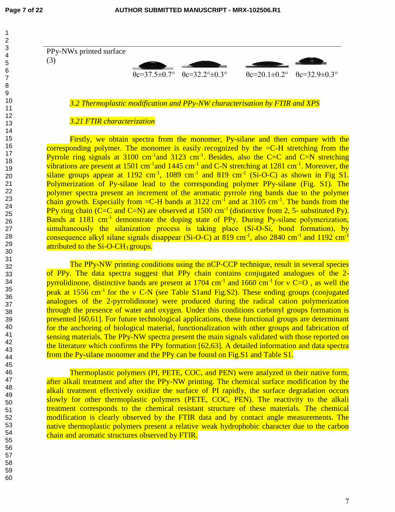
3.1. Characterization of PPy-NWs printed on thermoplastics by contact angle
measurements
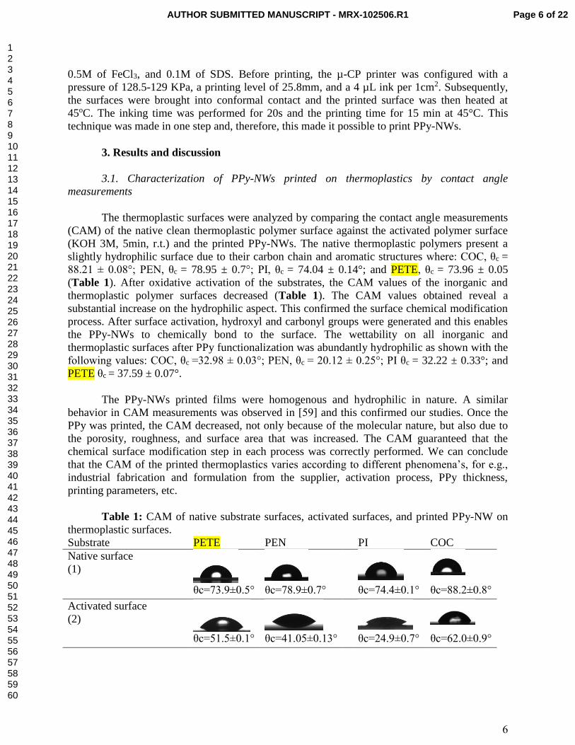
The thermoplastic surfaces were analyzed by comparing the contact angle measurements
(CAM) of the native clean thermoplastic polymer surface against the activated polymer surface
(KOH 3M, 5min, r.t.) and the printed PPy-NWs. The native thermoplastic polymers present a
slightly hydrophilic surface due to their carbon chain and aromatic structures where: COC, θc =
88.21 ± 0.08°; PEN, θc = 78.95 ± 0.7°; PI, θc = 74.04 ± 0.14°; and PETE, θc = 73.96 ± 0.05
(Table 1). After oxidative activation of the substrates, the CAM values of the inorganic and
thermoplastic polymer surfaces decreased (Table 1). The CAM values obtained reveal a
substantial increase on the hydrophilic aspect. This confirmed the surface chemical modification
process. After surface activation, hydroxyl and carbonyl groups were generated and this enables
the PPy-NWs to chemically bond to the surface. The wettability on all inorganic and
thermoplastic surfaces after PPy functionalization was abundantly hydrophilic as shown with the
following values: COC, θc =32.98 ± 0.03°; PEN, θc = 20.12 ± 0.25°; PI θc = 32.22 ± 0.33°; and
PETE θc = 37.59 ± 0.07°.
The PPy-NWs printed films were homogenous and hydrophilic in nature. A similar
behavior in CAM measurements was observed in [59] and this confirmed our studies. Once the
PPy was printed, the CAM decreased, not only because of the molecular nature, but also due to
the porosity, roughness, and surface area that was increased. The CAM guaranteed that the
chemical surface modification step in each process was correctly performed. We can conclude
that the CAM of the printed thermoplastics varies according to different phenomena’s, for e.g.,
industrial fabrication and formulation from the supplier, activation process, PPy thickness,
printing parameters, etc.
Table 1: CAM of native substrate surfaces, activated surfaces, and printed PPy-NW on
thermoplastic surfaces.
Substrate PETE PEN PI COC
Native surface
(1)
θc=73.9±0.5° θc=78.9±0.7° θc=74.4±0.1° θc=88.2±0.8°
Activated surface
(2)
θc=51.5±0.1° θc=41.05±0.13° θc=24.9±0.7° θc=62.0±0.9°
Page 6 of 22AUTHOR SUBMITTED MANUSCRIPT - MRX-102506.R1
123456789101112131415161718192021222324252627282930313233343536373839404142434445464748495051525354555657585960
7
PPy-NWs printed surface
(3)
θc=37.5±0.7° θc=32.2°±0.3° θc=20.1±0.2° θc=32.9±0.3°
3.2 Thermoplastic modification and PPy-NW characterisation by FTIR and XPS
3.21 FTIR characterization
Firstly, we obtain spectra from the monomer, Py-silane and then compare with the
corresponding polymer. The monomer is easily recognized by the =C-H stretching from the
Pyrrole ring signals at 3100 cm-1and 3123 cm-1. Besides, also the C=C and C=N stretching
vibrations are present at 1501 cm-1and 1445 cm-1 and C-N stretching at 1281 cm-1. Moreover, the
silane groups appear at 1192 cm-1, 1089 cm-1 and 819 cm-1 (Si-O-C) as shown in Fig S1.
Polymerization of Py-silane lead to the corresponding polymer PPy-silane (Fig. S1). The
polymer spectra present an increment of the aromatic pyrrole ring bands due to the polymer
chain growth. Especially from =C-H bands at 3122 cm-1 and at 3105 cm-1. The bands from the
PPy ring chain (C=C and C=N) are observed at 1500 cm-1 (distinctive from 2, 5- substituted Py).
Bands at 1181 cm-1 demonstrate the doping state of PPy. During Py-silane polymerization,
simultaneously the silanization process is taking place (Si-O-Si, bond formation), by
consequence alkyl silane signals disappear (Si-O-C) at 819 cm-1, also 2840 cm-1 and 1192 cm-1
attributed to the Si-O-CH3 groups.
The PPy-NW printing conditions using the nCP-CCP technique, result in several species
of PPy. The data spectra suggest that PPy chain contains conjugated analogues of the 2-
pyrrolidinone, distinctive bands are present at 1704 cm-1 and 1660 cm-1 for C=O , as well the
peak at 1556 cm-1 for the C-N (see Table S1and Fig.S2). These ending groups (conjugated
analogues of the 2-pyrrolidinone) were produced during the radical cation polymerization
through the presence of water and oxygen. Under this conditions carbonyl groups formation is
presented [60,61]. For future technological applications, these functional groups are determinant
for the anchoring of biological material, functionalization with other groups and fabrication of
sensing materials. The PPy-NW spectra present the main signals validated with those reported on
the literature which confirms the PPy formation [62,63]. A detailed information and data spectra
from the Py-silane monomer and the PPy can be found on Fig.S1 and Table S1.
Thermoplastic polymers (PI, PETE, COC, and PEN) were analyzed in their native form,
after alkali treatment and after the PPy-NW printing. The chemical surface modification by the
alkali treatment effectively oxidize the surface of PI rapidly, the surface degradation occurs
slowly for other thermoplastic polymers (PETE, COC, PEN). The reactivity to the alkali
treatment corresponds to the chemical resistant structure of these materials. The chemical
modification is clearly observed by the FTIR data and by contact angle measurements. The
native thermoplastic polymers present a relative weak hydrophobic character due to the carbon
chain and aromatic structures observed by FTIR.
Page 7 of 22 AUTHOR SUBMITTED MANUSCRIPT - MRX-102506.R1
123456789101112131415161718192021222324252627282930313233343536373839404142434445464748495051525354555657585960

8
After the oxidization of the surface, carbonyl and alcohol groups appear on the surface of
the thermoplastic polymers, as shown in several spectra (see supporting information). We also
observe by CA measurements these changes, after oxidative activation, the CA decrease and the
hydrophilicity increase. After chemical treatment of the thermoplastic surface, new groups are
present, carboxylic, carbonyl and alcohol groups allowing the bonding between the thermoplastic
surface and the Py-silane monomer. The presence of these groups was confirmed by FTIR and
XPS. The PPy-silane is bond to the thermoplastic surface through the silanization process (Si-O-
Si and Si-O-C bond formation). Simultaneously to the silanization process, the polymerization is
taking place, by consequence PPy-NW are strongly binding. During CA measurement, the PPy-
NW was observed as an increase of the hydrophilic character.
In resume the PI spectra is composed mainly by the main bands corresponding to the
imide carbonyl and aromatic signals. After surface chemical treatment, the PI is modified by the
opening of the maleimide type ring and new bands are presented due to the formation of amide
and carboxylic acid or carboxylate groups. These carboxylic groups allow the bonding between
the thermoplastic surface and the PPy silane. After printing of PPy-NWs on the PI surface the
spectra display distinctive conjugated Pyrrole cycle signals, as shown the Fig S4. Before
treatment, the PI spectra show at 1776 cm-1and 1717 cm-1 the C=O vibrations from the imide
group and the representative signals for C-N stretching observed at 1379 cm-1. Besides, signals at
884 cm-1 from the 1,2,4,5 tetra substituted benzenes of imide, due to the C-H out of plane
deformation vibration. The aromatic bands =C-H stretching were observed at 3000-3100 cm-1.
Also, the 1,4 substituted aromatic C-H out of plane deformation bands were present at 725 cm-1
and 820 cm-1. In addition, signals related to the C-O-C stretching appeared at 1117 cm-1and 1249
cm-1(see Table S2).
Subsequent to the chemical activation treatment, the PI film surface was modified and the
maleimide type ring is opened by consequence new bands appeared, the amide and the
carboxylic acid groups. After the chemical activation process, the ether aromatic signals persist,
nevertheless the imide signals decreased. Presence of amide groups is observed at 1649 cm-1
(amide band 1), 1555 cm-1(amide band II), also the carboxylate group (COO-) stretching
vibrations at 1585 cm-1 and 1408 cm-1. Furthermore, characteristic bands from the –OH groups
are present at 2800 cm-1and 3600 cm-1 (see Table S2). Subsequently to the printed PPy-NWs on
the PI surface, distinctive pyrrole cycle signals are observed, =C-H vibrations at 3125 cm-1, also
C=C and C=N stretching bands located at 1501 cm-1 and 1445 cm-1. Besides, the C-N stretching
bands were found at 1280 cm-1 and the C-H deformation vibrations at 728 cm-1. The CH2
vibrations from the aliphatic hydrocarbons were present at 2932 cm-1, 2888 cm-1 and 1445 cm-1.
Also, the presence of Si-O groups was present at 1087 cm-1, 1065 cm-1 and 1015 cm-1, as shown
on Fig S4.
The case of PETE, mainly peaks appear at 1716 cm-1 concerning the carbonyl vibrations
and ether groups from the terephthalate bands at 1252 cm-1 and 1126 cm-1. The aromatic benzene
ring bands appeared at 3056 cm-1, 1614 cm-1 and 1506 cm-1 from the =CH and C=C vibrations
respectively, and the C-H vibrations appeared at 727 cm-1. The ethylene chain vibrations peaks
are present at 2970 cm-1, 2907 cm-1 and 1471 cm-1 (see Fig S5).After chemical activation
treatment, the carbonyl bands increased considerably in intensity due to the opening of the
terephthalate ring, clearly seen at 1716 cm-1and 1252 cm-1. Moreover, bands from COO- are
Page 8 of 22AUTHOR SUBMITTED MANUSCRIPT - MRX-102506.R1
123456789101112131415161718192021222324252627282930313233343536373839404142434445464748495051525354555657585960
9
observed at 1585 cm-1 and 1408 cm-1, also –OH band appear at 2800-3600 cm-1. Following to the
PPy-NW printing, the PETE surface present the characteristic bands of the PPy-silane.
Distinctive vibrations for =C-H at 3128 cm-1and 727 cm-1. Representative signals for the PPy-
silane were observed at 3128 cm-1 from =CH vibrations, also the peaks at 1501 cm-1 and 1446
cm-1 assigned to C=C and C=N vibrations. The NC band was present at 1281 cm-1 (Fig S5).
Additionally, the standard bands for silane groups (Si-O-Si and Si-OH) were present at 1087 cm-
1, 1064 cm-1, and 1015 cm-1. The CH2 bands were observed at 2934 cm-1, 2888 cm-1, and 1460
cm-1. Besides, as mentioned before, for future applications porpoises the anchoring group 2-
pyrrolidone analogues units conjugated into the PPy chain are crucial. These group was also
observed at 1701 cm-1, 1653 cm-1, and 1560 cm-1 corresponding to the C=O and C-N vibrations.
The main data collected is summarized in Table S3.
The PEN polymer spectrum present the characteristic bands from naphthalene and the
aromatic signals from =CH stretching at 3064 cm-1, at 933 cm-1, 839 cm-1 and 765 cm-1 for the
out of plane deformation vibration, also C=C bands are present at 1602 cm-1, 1502 cm-1, 1182
cm-1,1134 cm-1 and 765 cm-1. Besides, the characteristic signals of the aromatic ester (–C-O-C
stretching) at 1251 cm-1, 1093 cm-1 and at 1712 cm-1 for C=O stretching. After the chemical
activation treatment, the PEN surface is modified opening the ester bonds. For that reason,
signals attributed to the C-O-C bonds at 1251 cm-1 and 1093 cm-1 were decreased. After PPy-NW
printing on PEN, the spectrum (Fig S6) present the PPy main bands, consisting in the aromatic
ring chain. Also, the standard silanes peaks were present as shown in Table S4.
The last case, the pure COC polymer film show the main peaks from the aliphatic chain
at 2920 cm-1 , 2859 cm-1 and 1456 cm-1 corresponding to the CH2 vibrations as shown in Fig S7.
After chemical activation treatment, carbonyl bands appear at 1746 cm-1, 1723 cm-1 and at 1657
cm-1, making possible the PPy-silane bonding. After PPy-NW printing, the bands from the
aromatic ring chain are presented at 3123 cm-1, 3102 cm-1 for =C-H stretching. The typical C=C
and C=N stretching are also observed at 1500 cm-1 and 1444 cm-1. Also, standard siloxane bands
were observed at 1088 cm-1, 1066 cm-1 and at 1020 cm-1 for Si-O-Si, confirming that the
polymerization and silanization process proceed successfully.
3.22 XPS characterization
The chemical composition of thermoplastics polymers (PI, PETE, PEN, and COC) was
studied by comparing the chemical activated surfaces against the thermoplastic PPy-NW printed
surfaces using X-ray Photoelectron Spectroscopy (XPS). For that porpoise we investigate the
XPS spectra for the chemical species: C1s, O1s, N1s, Si 2p, Fe 2p3, and Cl 2p. The results
obtained with the FTIR and CA measurements support the thermoplastic oxidation by the alkali
treatment, because the present of new carbonyl groups and their hydrophilic surface character,
also these species were observed by XPS high-resolution C 1s spectra. Similarly, the PPy-NW
present in XPS analysis new elements (N1s, Si 2p, Fe 2p3, and Cl 2p) and carbon species, which
can be also confirmed by FTIR (conjugate aromatic PPy ring and silane groups) and CA
measurements ( observed in the decrement of the CA and increment in the hydrophilicity of the
surface). The XPS main chemical species for the thermoplastic polymers are C1s, O1s, N1s. On
the other hand, the characteristic chemical species for the presence of PPy-NW are the N1s, Si 2p
Page 9 of 22 AUTHOR SUBMITTED MANUSCRIPT - MRX-102506.R1
123456789101112131415161718192021222324252627282930313233343536373839404142434445464748495051525354555657585960
10
corresponding to the Pyrrole monomer. Also, we observed the species Cl 2p and Fe 2p3, from
the catalyst.
For the case of the PI, we found the characteristic profile from the PI polymer [64],
however, after the activation the increment of O1s and C1s species corresponding to amine and
carboxylic groups increase, due to the imide ring opening, as shown in Fig S8. The PI activated
surface show distinctive peaks located at 284.1, 285.1, 287.4 eV correspond to the C–C/C–H, C–
O/C–O–C, O–C=O/C=O signals, respectively (Fig S9). After PPy-NW printing, new species are
observed (Cl 2p and Fe 2p3) assigned to the catalyst FeCl3, which reveals that the PPy-NW film
is on its oxidized state [65]. Besides, the presence of chlorine signals, probe the doping state of
the PPy as shown in Fig S9. The C1s signals (C-O) are reduced, while those in the C-C region
had increased (due to the polymer printing). The O1s, Si 2s and Si 2p signal increased due to the
presence silane groups (Si-O-Si), the O1s increase also due to the presence of terminal carbonyl
groups (2-pyrrolidone analogues) contained in the PPy-NW. The presence of the N1s, Si 2p, Cl
2p, and Fe 2p3 species and also the O1s increment content while the C1s suggest that the
PPyNW were successfully printed on the thermoplastic surface. The elemental analysis and the
data are summarized in Table S7.
The XPS analysis for the PETE activated surface show an oxidized surface due to the
presence of C–C/C–H, C–O/C–O–C, O–C=O/C=O signals at 284, 285.5 and 288.4 eV,
respectively (Fig S11a). Subsequently to the PPy-NW printing, PETE surface show the C–O/C–
O–C and O–C=O/C=O signals at 285.5 and 287.8 eV, respectively. The main difference can be
observed in carbon content, especially the species related with the carboxylate groups decrease
(C-O, C=O) due to the presence of N1s, Si 2p, Fe 2p3, and Cl 2p as shown in Fig S11.
The case of the PEN, XPS analysis for the activated surface, signals from C–C/C–H, C–
O/C–O–C, O–C=O/C=O at 284.4, 286, and 288.55 eV can be observed, as shown in Fig S13a.
These signals are result of the naphthalene rings disruption producing an aliphatic-like species,
also due to ester group disruption, generating carbonyl groups. Moreover, PEN printed with PPy-
NW shows characteristic C–C/C–H, C–O/C–O–C, O–C=O/C=O signals at 284.6, 286, 288.4 eV,
respectively (see Fig S13b).The PPy-NW printing produced an increment on the signals for C-C
and C=O and C-O decrement.
The XPS analysis for the COC chemical modified surface present the profile of an
untreated COC film, C 1s specie at 532.8 eV [66], also we can observe the presence of oxygen as
shown in Fig S14. The COC oxidize surface mainly present peaks from C–C/C–H, C–O/C–O–C,
O–C=O/C=O at 283.3, 285, 286.35 eV (see Fig S15a). After PPy-NW printing on the COC
surface film, PPy-NW characteristics signals were observed (Si 2p, N1s, Cl 2p and Fe 2p3).The
species corresponding to the oxidized and COC chain surface were observed, C–C/C–H, C–O/C–
O–C at 284.5, 285.5 eV, respectively (see Fig S15b).
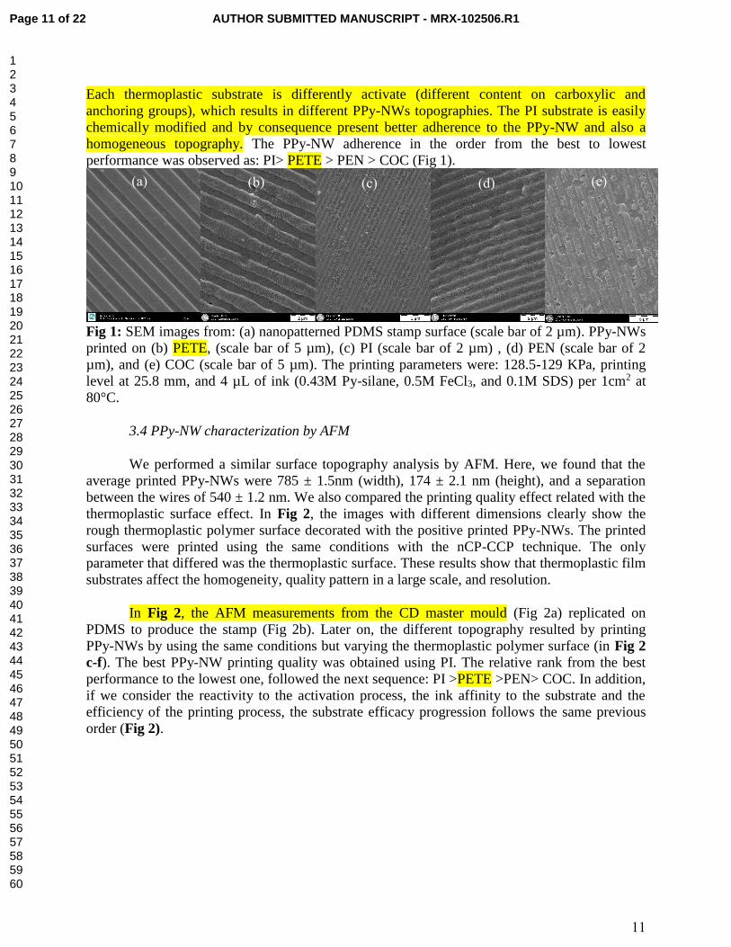
3.3 PPy-NW characterization by SEM
The influence of the thermoplastic polymers in the PPy-NW topography was observed by
scanning electron microscopy (SEM). The thermoplastic polymers reacted differently to the
activation with basic treatment (KOH), as presented before in FTIR and XPS characterization
Page 10 of 22AUTHOR SUBMITTED MANUSCRIPT - MRX-102506.R1
123456789101112131415161718192021222324252627282930313233343536373839404142434445464748495051525354555657585960
11
Each thermoplastic substrate is differently activate (different content on carboxylic and
anchoring groups), which results in different PPy-NWs topographies. The PI substrate is easily
chemically modified and by consequence present better adherence to the PPy-NW and also a
homogeneous topography. The PPy-NW adherence in the order from the best to lowest
performance was observed as: PI> PETE > PEN > COC (Fig 1).
Fig 1: SEM images from: (a) nanopatterned PDMS stamp surface (scale bar of 2 µm). PPy-NWs
printed on (b) PETE, (scale bar of 5 µm), (c) PI (scale bar of 2 µm) , (d) PEN (scale bar of 2
µm), and (e) COC (scale bar of 5 µm). The printing parameters were: 128.5-129 KPa, printing
level at 25.8 mm, and 4 µL of ink (0.43M Py-silane, 0.5M FeCl3, and 0.1M SDS) per 1cm2 at
80°C.
3.4 PPy-NW characterization by AFM
We performed a similar surface topography analysis by AFM. Here, we found that the
average printed PPy-NWs were 785 ± 1.5nm (width), 174 ± 2.1 nm (height), and a separation
between the wires of 540 ± 1.2 nm. We also compared the printing quality effect related with the
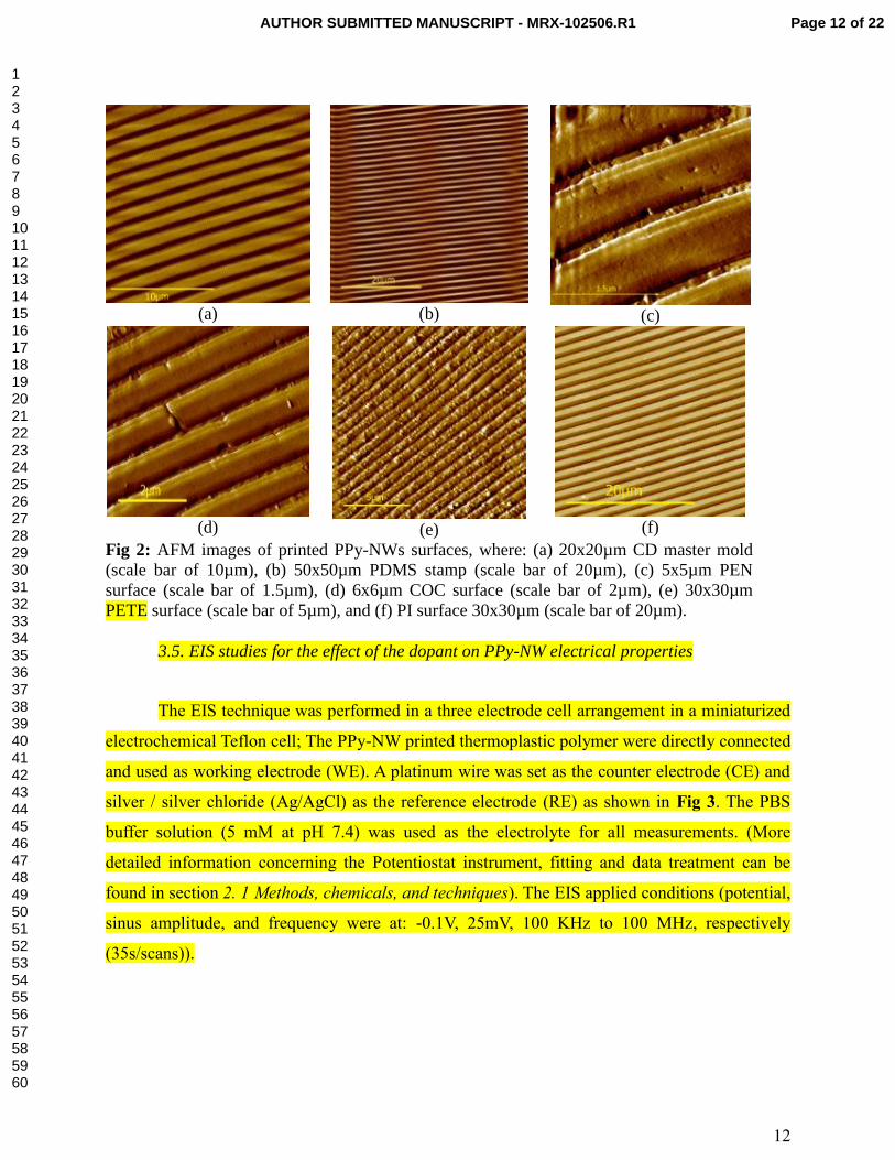
thermoplastic surface effect. In Fig 2, the images with different dimensions clearly show the
rough thermoplastic polymer surface decorated with the positive printed PPy-NWs. The printed
surfaces were printed using the same conditions with the nCP-CCP technique. The only
parameter that differed was the thermoplastic surface. These results show that thermoplastic film
substrates affect the homogeneity, quality pattern in a large scale, and resolution.
In Fig 2, the AFM measurements from the CD master mould (Fig 2a) replicated on
PDMS to produce the stamp (Fig 2b). Later on, the different topography resulted by printing
PPy-NWs by using the same conditions but varying the thermoplastic polymer surface (in Fig 2
c-f). The best PPy-NW printing quality was obtained using PI. The relative rank from the best
performance to the lowest one, followed the next sequence: PI >PETE >PEN> COC. In addition,
if we consider the reactivity to the activation process, the ink affinity to the substrate and the
efficiency of the printing process, the substrate efficacy progression follows the same previous
order (Fig 2).
(a) (b) (c) (d) (e)
Page 11 of 22 AUTHOR SUBMITTED MANUSCRIPT - MRX-102506.R1
123456789101112131415161718192021222324252627282930313233343536373839404142434445464748495051525354555657585960
12
(a)
(b)
(c)
(d)
(e)
(f)
Fig 2: AFM images of printed PPy-NWs surfaces, where: (a) 20x20µm CD master mold
(scale bar of 10µm), (b) 50x50µm PDMS stamp (scale bar of 20µm), (c) 5x5µm PEN
surface (scale bar of 1.5µm), (d) 6x6µm COC surface (scale bar of 2µm), (e) 30x30µm
PETE surface (scale bar of 5µm), and (f) PI surface 30x30µm (scale bar of 20µm).
3.5. EIS studies for the effect of the dopant on PPy-NW electrical properties
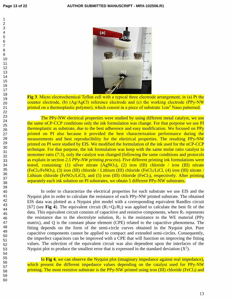
The EIS technique was performed in a three electrode cell arrangement in a miniaturized
electrochemical Teflon cell; The PPy-NW printed thermoplastic polymer were directly connected
and used as working electrode (WE). A platinum wire was set as the counter electrode (CE) and
silver / silver chloride (Ag/AgCl) as the reference electrode (RE) as shown in Fig 3. The PBS
buffer solution (5 mM at pH 7.4) was used as the electrolyte for all measurements. (More
detailed information concerning the Potentiostat instrument, fitting and data treatment can be
found in section 2. 1 Methods, chemicals, and techniques). The EIS applied conditions (potential,
sinus amplitude, and frequency were at: -0.1V, 25mV, 100 KHz to 100 MHz, respectively
(35s/scans)).
Page 12 of 22AUTHOR SUBMITTED MANUSCRIPT - MRX-102506.R1
123456789101112131415161718192021222324252627282930313233343536373839404142434445464748495051525354555657585960
13
Fig 3. Micro electrochemical Teflon cell with a typical three electrode arrangement, in (a) Pt the
counter electrode, (b) (Ag/AgCl) reference electrode and (c) the working electrode (PPy-NW
printed on a thermoplastic polymer), which consist in a piece of substrate 1cm2 Nano patterned.
The PPy-NW electrical properties were studied by using different metal catalyst, we use
the same nCP-CCP conditions only the ink formulation was change. For that porpoise we use PI
thermoplastic as substrate, due to the best adherence and easy modification. We focused on PPy
printed on PI also because it provided the best characterization performance during the
measurements and best reproducibility for the electrical properties. The resulting PPy-NW
printed on PI were studied by EIS. We modified the formulation of the ink used for the nCP-CCP
technique. For that purpose, the ink formulation was keep with the same molar ratio catalyst to
monomer ratio (7:3), only the catalyst was changed (following the same conditions and protocols
as explain in section 2.5 PPy-NW printing process). Five different printing ink formulations were
tested, containing: (1) silver nitrate (AgNO3), (2) iron (III) chloride / iron (III) nitrate
(FeCl3/FeNO3), (3) iron (III) chloride / Lithium (III) chloride (FeCl3/LiCl, (4) iron (III) nitrate /
Lithium chloride (FeNO3/LiCl), and (5) iron (III) chloride (FeCl3), respectively. After printing
separately each ink solution on PI substrates, we obtain 5 different PPy-NW substrates.
In order to characterize the electrical properties for each substrate we use EIS and the
Nyquist plot in order to calculate the resistance of each PPy-NW printed substrate. The obtained
EIS data was plotted as a Nyquist plot model with a corresponding equivalent Randles circuit
[67] (see Fig 4). The equivalent circuit (R1+Q2/R2) was applied to calculate the best fit of the
data. This equivalent circuit consists of capacitive and resistive components, where R1 represents
the resistance due to the electrolyte solution, R2 is the resistance to the WE material (PPy
matrix), and Q is the constant phase element (CPE) related to the capacitive phenomena. The
fitting depends on the form of the semi-circle curves obtained in the Nyquist plot. Pure
capacitive components cannot be applied to compact and extended semi-circles. Consequently,
the imperfect capacitors can be improved with a CPE that will function on improving the fitting
values. The selection of the equivalent circuit was also dependent upon the interfaces of the
Nyquist plot to produce the smallest error that is expressed in the standard deviation (X2).
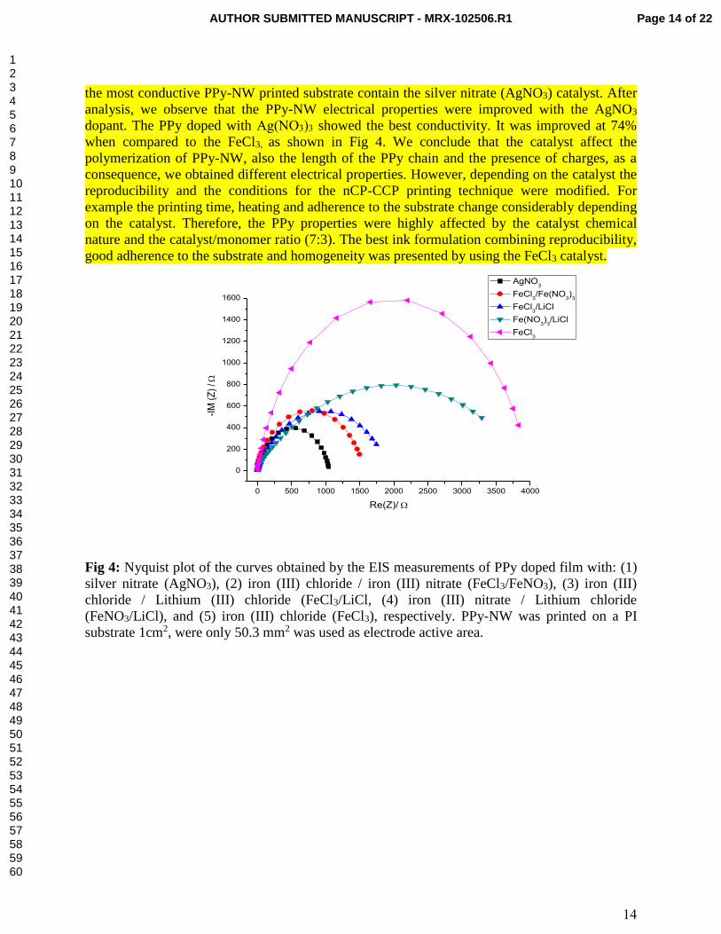
In Fig 4, we can observe the Nyquist plot (imaginary impedance against real impedance),
which present the different impedance values depending on the catalyst used for PPy-NW
printing. The most resistive substrate is the PPy-NW printed using iron (III) chloride (FeCl3) and
Page 13 of 22 AUTHOR SUBMITTED MANUSCRIPT - MRX-102506.R1
123456789101112131415161718192021222324252627282930313233343536373839404142434445464748495051525354555657585960
14
the most conductive PPy-NW printed substrate contain the silver nitrate (AgNO3) catalyst. After
analysis, we observe that the PPy-NW electrical properties were improved with the AgNO3
dopant. The PPy doped with Ag(NO3)3 showed the best conductivity. It was improved at 74%
when compared to the FeCl3, as shown in Fig 4. We conclude that the catalyst affect the
polymerization of PPy-NW, also the length of the PPy chain and the presence of charges, as a
consequence, we obtained different electrical properties. However, depending on the catalyst the
reproducibility and the conditions for the nCP-CCP printing technique were modified. For
example the printing time, heating and adherence to the substrate change considerably depending
on the catalyst. Therefore, the PPy properties were highly affected by the catalyst chemical
nature and the catalyst/monomer ratio (7:3). The best ink formulation combining reproducibility,
good adherence to the substrate and homogeneity was presented by using the FeCl3 catalyst.
Fig 4: Nyquist plot of the curves obtained by the EIS measurements of PPy doped film with: (1)
silver nitrate (AgNO3), (2) iron (III) chloride / iron (III) nitrate (FeCl3/FeNO3), (3) iron (III)
chloride / Lithium (III) chloride (FeCl3/LiCl, (4) iron (III) nitrate / Lithium chloride
(FeNO3/LiCl), and (5) iron (III) chloride (FeCl3), respectively. PPy-NW was printed on a PI
substrate 1cm2, were only 50.3 mm2 was used as electrode active area.
0 500 1000 1500 2000 2500 3000 3500 4000
0
200
400
600
800
1000
1200
1400
1600
-IM
(Z
) /
Re(Z)/
AgNO3
FeCl3/Fe(NO
3)3
FeCl3/LiCl
Fe(NO3)3/LiCl
FeCl3
Page 14 of 22AUTHOR SUBMITTED MANUSCRIPT - MRX-102506.R1
123456789101112131415161718192021222324252627282930313233343536373839404142434445464748495051525354555657585960
15
After EIS measurements, the data obtained through the Nyquist plot (Fig 4) was fitted
and the values for the resistance from the electrolyte solution (R1), the resistance from the PPy
matrix (R2), and the constant phase element (Q) were calculated. The fitting error was expressed
as standard deviation (X2) as shown in Table 2. Here in Table 2, the different electric PPy
properties can be observed depending on the catalyst and expressed as (R2) values. In order to
compare the PPy electrical properties, we calculate the relative resistance ratio R2 (resistance of
the material R2 divided by the FeCl3 resistance).
The electrical properties from the PPy obtained can be presented in decreasing order of
conductivity as AgNO3 > FeCl3/FeNO3 > FeCl3/LiCl > FeNO3/LiCl > FeCl3. As exposed before
the most conductive PPy-NW printed on PI contain the AgNO3 catalyst, almost four times more
conductive as shown in Table 2. However, this catalyst requires higher printing time and heating
(30 min 70oC), we also observe relative less adherence in comparison to the FeCl3 catalyst. Also,
we can observe that both catalyst have a higher constant phase element, which reflects the
favorable charge accumulation and doping state of the polymer on solution. Future work will be
focus on the optimization of the printing using the silver catalyst. As a final point, during the EIS
studies, we observed that there was no electrical effect when PPy-NW was printed on the
different thermoplastic films. However, adherence surface topography and homogeneity is
affected.
Table 2: Fitting parameters obtained from the equivalent circuit (R1+Q2/R2) for the PPy with
different dopants.
Catalyst R1(Ω) R2(Ω)
Q2 (F.s^(a-1)) X2 Relative R2 to
FeCl3
AgNO3 1769 1057 50.12±82x10-6 0.00421 3.84
FeCl3/ Fe(NO3)3 3985 1598 29.16±78x10-6 0.00119 2.54
FeCl3/ LiCl 4674 1943 12.40±66x10-6 0.00128 2.09
FeCl3 6922 4064 79.30±47x10-6 0.00067 1
Fe(NO3)3/ LiCl 1782 3979 16.98±85x10-6 0.00848 1.02
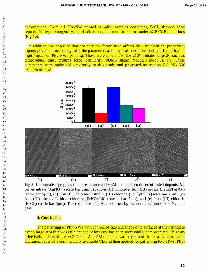
3.5. Catalyst effect on PPy-NW morphology, characterization by SEM
In this section we show how the topography and surface morphology of PPy-NW is
affected by the use of different catalyst printed by nCP-CCP technique. As described before, the
same printing parameters were used. Depending on the ink composition (catalyst) employed,
different PPy electrical properties are obtained. In Fig 5, a comparative graphic show the
different PPy conductivities obtained for each dopant (more detailed in previous section). Also,
we can observe how dopant affects the PPy-NWs topography and the surface morphology. The
AFM measurements suggest that the catalyst drive the aggregation during polymerization. The
topography obtained with the AgNO3 catalyst (Fig 5a) produced well-shaped PPy-NWs.
Besides, grains and crystals were found over the surface and especially between the channels. A
similar characteristics were found for the FeCl3/ Fe(NO3)3 dopant (Fig 5b), a highly rough
topography is observed and grains on the top of the PPy-NWs are deposited. Moreover, a more
homogeneous surface was observed for catalyst based on Lithium chloride (Fig 4c/d), also
almost no grains were observed. Also, PPy-NWs presented imperfections and shape
Page 15 of 22 AUTHOR SUBMITTED MANUSCRIPT - MRX-102506.R1
123456789101112131415161718192021222324252627282930313233343536373839404142434445464748495051525354555657585960
16
deformations. From all PPy-NW printed samples, samples containing FeCl3 showed good
reproducibility, homogeneity, good adherence, and ease to control under nCP-CCP conditions
(Fig 5e).
In addition, we observed that not only ink formulation affects the PPy electrical properties,
topography and morphology, also the parameters and physical conditions during printing have a
high impact on PPy-NWs printing. These were inherent to the µCP limitations (µCP) such as
temperature, time, printing force, capillarity, PDMS stamp, Young’s modulus, etc. These
parameters were optimized previously to this study and presented on section 2.5 PPy-NW
printing process.
0
500
1000
1500
2000
2500
3000
3500
4000
4500
(d) (a) (e) (c) (b)
Re(
Z)/
(a) (b) (c) (d) (e)
Fig 5: Comparative graphics of the resistance and SEM images from different tested dopants: (a)
Silver nitrate (AgNO3) (scale bar 1µm), (b) Iron (III) chloride/ Iron (III) nitrate (FeCl3/FeNO3)
(scale bar 5µm), (c) Iron (III) chloride/ Lithium (III) chloride (FeCl3/LiCl) (scale bar 2µm), (d)
Iron (III) nitrate/ Lithium chloride (FeNO3/LiCl) (scale bar 2µm), and (e) Iron (III) chloride
(FeCl3) (scale bar 5µm). The resistance data was obtained by the normalization of the Nyquist
plot.
4. Conclusion
The patterning of PPy-NWs with controlled size and shape onto surfaces at the nanoscale
over a large area that was efficient and at low cost has been successfully demonstrated. This was
effectively achieved by nCP-CCP. A PDMS stamp was replicated from a nanopatterned
aluminum layer of a commercially available CD and then applied for patterning PPy-NWs. PPy-
Page 16 of 22AUTHOR SUBMITTED MANUSCRIPT - MRX-102506.R1
123456789101112131415161718192021222324252627282930313233343536373839404142434445464748495051525354555657585960
17
NW and the thermoplastic substrates were successfully characterized. The chemical modification
was verified by CAM, demonstrating that the alkali treatment produce a hydrophilic surface by
the creation of carboxylic groups, also observed on FTIR and XPS. The PPy-NW printed present
an adherence in the order from the best to lowest performance as: PI> PETE > PEN > COC. We
keep PI as the best substrate for PPy-NW printing. Subsequently to the PPy-NW printing the
PPy-silane polymerization and silanization process was verified. We observe the PPy conjugated
ring signals (C=C, C=N, C-N), and the distinctive bands from 2, 5- substituted Pyrrole by FTIR
and XPS. Also, we demonstrate the doping state of PPy by FTIR. Besides, we observe the
presence of silane bond formation (Si-O-Si). Finally the ink formulation was modified by using
different catalyst based on Iron and Silver salts, obtaining the best PPy-NW conductivity using
silver nitrate. Different topography characteristics were observed by SEM, AFM, depending on
the catalyst employed. The PPy-NW printed using the ink formulation based on FeCl3 showed
good reproducibility, homogeneity, good adherence, and ease to control under nCP-CCP
conditions, as consequence FeCl3 was chosen as catalyst.
The developed methodology for molecule patterning can be of great interest in those
areas that require nanoscale structures over large areas, such as tissue engineering or biosensor
applications. The Nanopatterning on PETE, COC, PEN, and PI substrates can be useful for
Nanoengineering of electrical devices using PPy as the conductive nanomaterial, opening the
possibility to use the same nCP-CCP technique for others molecules(e.g. aniline, thiophene etc).
To our knowledge, we have developed new sub-micrometer printing technique. Future work will
be the development of Impedimetric and nanoFET sensors based on PPy-NWs.
*Supporting Information
Detailed information concerning FTIR measurements, XPS spectroscopy, and additional
results from the surface characterization is available.
Acknowledgements
The authors would like to thank to CONACYT (Mexican National Council of Science
and Technology) Scholarship Program, the SMARTCANCERSENS project (FP7-PEOPLE-
2012-IRSES) under the grant agreement No. 31805, the SEA-on-a-CHIP project (FP7-KBBE)
under the reference 614168, and the NATO project, SPS (NUKP.SFPP984173) and it reflects
only the author’s views.
References
[1]Cui, Y., Wei Q., Park H., Lieber C.M.; Science 2001, 293 (5533),1289–92.
[2] Ramanathan, K.; Bangar, M. A.; Yun, M.; Chen W.; Myung, N. V.; Mulchandani, A., Journal of the
American Chemical Society 2005, 127 (2) , 496–97.
[3] Sarkar, T.; Gao, Y.; Mulchandani, A., Applied Biochemistry and Biotechnology 2013, 170(5), 1011–
25.
Page 17 of 22 AUTHOR SUBMITTED MANUSCRIPT - MRX-102506.R1
123456789101112131415161718192021222324252627282930313233343536373839404142434445464748495051525354555657585960
18
[4] Ariga, K.; Kroto, H.; and O’Brien, P., Manipulation of Nanoscale Materials: An Introduction to
Nanoarchitectonics 2012 (Royal Society of Chemistry).
[5] Cao, G.; Wang, Y., Nanostructures and Nanomaterials: Synthesis, Properties, and Applications2011,
World Scientific.
[6] Kong, J.; Franklin, N. R.; Zhou, C.; Chapline, M. G.; Peng, S.; Cho, K.; Dai, H., Science 2000,
287(5453), 622–25.
[7] Zheng, G.; Patolsky, F.; Cui, Y.; Wang, W. U.; Lieber, C. M., Nature Biotechnology 2005, 23 (10),
1294–1301.
[8] Law, M.; Kind, H.; Messer, B.; Kim, F.; Yang, P., Angewandte Chemie International Edition 2002,
41(13), 2405–8.
[9] Li, C.; Zhang, D.; Liu X.; Han, S.; Tang, T.; Han, J. and Zhou, C.; Applied Physics Letters 2003,
82(10), 1613–15.
[10] He, H. X.; Tao, N. J., Electrochemical Fabrication of Metal Nanowires in Encyclopedia of
Nanoscience and Nanotechnology, 2003, Eds., NS Nalwa (American Scientific Publishers).
[11] Patolsky, F.; Zheng, G.; Lieber, C. M., Nature Protocols 2006, 1(4) ,1711–24.
[12] Kong, J.; Franklin, N. R.; Zhou, C.; Chapline, M. G.; Peng, S.; Cho, K.; Dai, H., Science 2000, 28
(287), 5453, 622-625;
[13] Boussaad; S.; Tao, N. J., Nano Letters 2003, 3 (8),1173–76.
[14] Roschier, L.; Penttilä, J.; Martin M.; Hakonen, P.; Paalanen, M.; Tapper, U.; Kauppinen, E. I.;
Journet, C.; Bernier, P., Applied Physics Letters 1999, 75 (5), 728–30.
[15] Tans, S. J.; Verschueren, A. R. M.; Dekker, C., Nature 1998, 393 (6680) ,49–52.
[16] Franklin, N. R., Wang, Q., Tombler, T. W., Javey, A., Shim, M. and Dai, H.; Integration of
Suspended Carbon Nanotube Arrays into Electronic Devices and Electromechanical Systems, Applied
Physics Letters 2002, 81 (5), 913–15.
[17] MacDiarmid, A. G., Synthetic Metals: A Novel Role for Organic Polymers. The Nobel Foundation
2001. Angewandte Chemie 2001, 40 (14), 2581-2590.
[18]Akagi K., Shirakawa H., Araya K., Mukoh A., Narahara T., Highly Conductive Polyacetylene Film
Prepared by the Liquid Crystal Polymerization Method under Magnetic Field, Synthetic Metals 1987, 17
(1), 241–46.
[19] K. Lee, S. Cho, S.H. Park, A.J. Heeger, C.W. Lee, S.H. Lee, Metallic Transport in Polyaniline;
Nature 2006, 441 (7089), 65–68.
Page 18 of 22AUTHOR SUBMITTED MANUSCRIPT - MRX-102506.R1
123456789101112131415161718192021222324252627282930313233343536373839404142434445464748495051525354555657585960
19
[20] H. Yoon and J. Jang, Conducting-Polymer Nanomaterials for High-Performance Sensor
Applications: Issues and Challenges, Advanced Functional Materials 2009, 19 (10): 1567–76.
[21] Yoon, H., Lee, S., Kwon, O., Song, H., Oh, E., Park, T. and Jang, J., Polypyrrole Nanotubes
Conjugated with Human Olfactory Receptors: High-Performance Transducers for FET-Type
Bioelectronic Noses, Angewandte Chemie 2009, 48 (15), 2755–58.
[22] Xie, H.; Luo, S. C.; Yu, H. H., Small 2009, 5 (22), 2611–17.
[23] Bangar, M. A., Analytical Chemistry 2009, 81 (6), 2168–75.
[24] Ramanathan, K.; Bangar, M.A.; Yun, M.; Chen, W.; Mulchandani A.; Myung, N. V., Electroanalysis
2007, 19 (7–8) , 793–97.
[25] Ramanathan, K.; Bangar, M.A.; Yun, M.; Chen, W.; Mulchandani, A.; Myung, N. V., Nano Letters
2004, 4(7), 1237–39.
[26] J. H. Lim and C. A. Mirkin, Electrostatically Driven Dip-Pen Nanolithography of Conducting
Polymers, Advanced Materials 2002, 14 (20), 1474–1477.
[27] He, H. X.; Li, C. Z.; Tao, N. J., Applied Physics Letters 2001, 78 (6) , 811–13.
[28] Liu, S. L.; Long, Y. Z.; Zhang, Z.H.; Zhang, H. D.; Bin, S.; Zhang, J. C.; Han, W. P., Journal of
Nanomaterials 2013,(2013) , 713275.
[29] Ge, D.; Wang, J.; Wang, S.; Ma, J.; He, B.; Journal of Materials Science Letters 2003, 22 (11) , 839–
40.
[30] Martin C. R., Chemistry of Materials 1996, 8(8), 1739–46.
[31] Martin C. R., Abstracts of Papers of the American Chemical Society 1995, 210,39.
[32] Massuyeau, F.; Duvail, J. L.; Athalin, H.; Lorcy, J. M.; Lefrant, S.; Wéry, J.; Faulques, E.;
Nanotechnology 2009, 20 (15), 155701.
[33] Chen, X.; Sun, J.; Shen, J., Langmuir: The ACS Journal of Surfaces and Colloids 2009, 25 (5),
3316–20.
[34] Dong, B.; Krutschke, M.; Zhang, X.; Chi, L.; Fuchs, H., Small 2005, 1(5) ,520–24.
[35] Omastová, M.; Trchová, M.; Kovářová, J.; Stejskal, J., Synthetic Metals 2003, 138 (3), 447–55.
[36] Jung, M. H.; Lee, H., Langmuir: The ACS Journal of Surfaces and Colloids 2008, 24 (17), 9825–31.
[37] Caballero, D.; Fumagalli, L.; Teixidor, F.; Samitier, J.; Errachid, A., Sensors and Actuators B-
Chemical 2013, 177,1003-1009.
Page 19 of 22 AUTHOR SUBMITTED MANUSCRIPT - MRX-102506.R1
123456789101112131415161718192021222324252627282930313233343536373839404142434445464748495051525354555657585960
20
[38] Errachid, A.; Caballero, D.; Crespo, E.; Bessueille, F.; Pla-Roca, M.; Mills, C. A, Teixidor, F.;
Samitier J., Nanotechnology 2007, 18 (48), 485301.
[39] Garcia-Cruz, A.; Zine N.; Sigaud, M.; Lee, M.; Marote, P.; Lanteri, P.; Bausells, J.; Errachid, A.,
Microelectronic Engineering 2014, 121, 167-174.
[40] Garcia-Cruz A.; Lee, M.; Zine N.; Sigaud, M.; Bausells, J.; Errachid, A., Poly(pyrrole) Microwires
Fabrication Process on Flexible Thermoplastics Polymers: Application as a Biosensing, Sensors and
Actuators B: Chemical 2015,221, 940-950.
[41] Mukherjee, R.; Pangule, R. C.; Sharma, A.; Banerjee, I.; The Journal of Chemical Physics 2007,
127(6), 064703.
[42] Meenakshi, V.; Babayan, Y.; Odom, T.W., Journal of Chemical Education 2007, 84, 1795.
[43] Chowdhury, D.; Paul, A.; Chattopadhyay, A., Nano Letters 2001, 1(8), 409–12.
[44] Baraketa A., Zinean N., Lee M., Bausells J., Jaffrezic-Renault N., Bessueille F., Yaakoubi N., A.
Errachid, Development of a Flexible Microfluidic System Based on a Simple and Reproducible Sealing
Process between Polymers and Poly(dimethylsiloxane), Microelectronic Engineering 2013, 111, 332–38.
[45] Lee M., Lopez-Martinez M. J., Baraket A., Zine N., Esteve J., Plaza J. A., Jaffrezic-Renault N. and
Errachid A., ,Polymer Micromixers Bonded to Thermoplastic Films Combining Soft-Lithography with
Plasma and Aptes Treatment Processes, Journal of Polymer Science Part a-Polymer Chemistry 2013,
51,1, 59–70.
[46] Pino M., Stingelin N., and Tanner K. E., Nucleation and Growth of Apatite on NaOH-Treated PEEK,
HDPE and UHMWPE for Artificial Cornea Materials, Acta Biomaterialia 2008, 4 (6), 827–36.
[47] Zhou H., Goel V. K., and Bhaduri S. B., A Fast Route to Modify Biopolymer Surface: A Study on
Polyetheretherketone (PEEK), Materials Letters 2014, 125, 96–98.
[48] Hadjizadeh A., Ajji A., and Bureau M. N., Preparation and Characterization of NaOH Treated
Micro-Fibrous Polyethylene Terephthalate Nonwovens for Biomedical Application, Journal of the
Mechanical Behavior of Biomedical Materials 2010, 3(8), 574–83.
[49] Ng R., Zhang X., Liu N., Yang S. T., Modifications of Nonwoven Polyethylene Terephthalate
Fibrous Matrices via NaOH Hydrolysis: Effects on Pore Size, Fiber Diameter, Cell Seeding and
Proliferation, Process Biochemistry 2009, 44 (9), 992–98.
[50] Karayannidis G. P., Chatziavgoustis A. P., and Achilias D. S., Poly(ethylene Terephthalate)
Recycling and Recovery of Pure Terephthalic Acid by Alkaline Hydrolysis, Advances in Polymer
Technology 2002, 21 (4), 250–59.
Page 20 of 22AUTHOR SUBMITTED MANUSCRIPT - MRX-102506.R1
123456789101112131415161718192021222324252627282930313233343536373839404142434445464748495051525354555657585960
21
[51] Hammouri, G.; Dana, A.; Sunar, B., Cryptographic Hardware and Embedded Systems - CHES 2009,
ed. Christophe Clavier and Kris Gaj, Lecture Notes in Computer Science 5747 (Springer Berlin
Heidelberg), 348–62.
[52] Cracauer R., Ganske R., Goh M., Goh J., Liederman A., Loo R., Tam P., Method and apparatus for
micro-contact printing, US20050139103 A1, issued June 30, 2005.
[53] Schmid H., Michel B., Kloter U., Keller G., Cano J.P., Stamp for patterning, method for
manufacturing such stamp and method for manufacturing an object using the stamp, US8268544 B2,
issued September 18, 2012.
[54] Graciela Beatriz Blanchet, Hee Hyun Lee, and Gary Delmar Jaycox, Method to form a pattern of
functional material on a substrate, WO2008042079 A2, issued April 10, 2008.
[55]Brian T. Mayers, Jeffrey Carbeck, and Karan Chauhan, Contact printing method using an elastomeric
stamp having a variable surface area and variable shape, WO2009014717 A1, issued January 29, 2009.
[56]Mukherjee R., Pangule R. C., Sharma A. and Banerjee I., Contact Instability of Thin Elastic Films on
Patterned Substrates, The Journal of Chemical Physics 2007, 127(6), 064703.
[57]Meenakshi V., Babayan Y., and Odom T.W., Benchtop Nanoscale Patterning Using Soft
Lithography. J. Chem. Educ., 2007, 84 (11), 1795-1798.
[58] Chowdhury D., Paul A., and Chattopadhyay A., Patterning Design in Color at the Submicron Scale.
Nano Letters, 2001, 1 (8), 409–412
[59] Thombare J.V., Rath M.C., Han S.H., Fulari V.J., Synthesis of hydrophilic polypyrrole thin films by
silar method, Materials Physics and Mechanics 2013, 16,118–25.
[60] Brezoi, D.V.; Brezoi, V., Journal of Science and Arts 2010, 1(12), 53–58.
[61] Ramelow, U. S.; Ma, J. H.; Darbeau, R., Material Research Innovations 2001, 5 (1), 40–49.
[62] P. Saville, “Polypyrrole Formation and Use, Defence R&D Canada” – Atlantic,Technical
Memorandum 2005, DRDC Atlantic.
[63] Chougule, M. A.; Pawar, S.G.; Godse, P. R.; Mulik, R. N.; Sen, S.; Patil, V. B., Soft
Nanoscience Letters 2011, 1, 6-10.
[64] Wang, P. S.; Wittberg, T. N.; Wolf, J. D.; Journal of Materials Science 1998, 23 (11),
3987–91,
[65] Qiao, Y.; Shen, L.; Guo, Y., Materials Letters 2012, 86, 38–41.
Page 21 of 22 AUTHOR SUBMITTED MANUSCRIPT - MRX-102506.R1
123456789101112131415161718192021222324252627282930313233343536373839404142434445464748495051525354555657585960

22
[66] S. J. Hwang; M. C. Tseng; J. R. Shu; H. H. Yu, Surface and Coatings Technology 2008, 202
(15), 3669–74.
[67] Randles, J. E. B., Discussions of the Faraday Society 1947, 1(0), 11–19.
Page 22 of 22AUTHOR SUBMITTED MANUSCRIPT - MRX-102506.R1
123456789101112131415161718192021222324252627282930313233343536373839404142434445464748495051525354555657585960


![The intricacies of the stacking interaction in a pyrrole ... · The intricacies of the stacking interaction in a pyrrole–pyrrole system Tomasz Sieran´ski1 Received: ... [32, 33]](https://img.pdfslide.net/doc/110x75/5ea942711f125e3c163555f9/the-intricacies-of-the-stacking-interaction-in-a-pyrrole-the-intricacies-of.jpg)

![119 Nanowires 4. Nanowires - UFAMhome.ufam.edu.br/berti/nanomateriais/Nanowires.pdf · 119 Nanowires 4. Nanowires ... written about carbon nanotubes [4.57–59], which can be](https://img.pdfslide.net/doc/110x75/5abfd11e7f8b9a5d718eba2b/119-nanowires-4-nanowires-nanowires-4-nanowires-written-about-carbon-nanotubes.jpg)