Embed Size (px)
Citation preview
Large-scale, heterogeneous integration of nanowirearrays for image sensor circuitryZhiyong Fan*†‡, Johnny C. Ho*†‡, Zachery A. Jacobson*†, Haleh Razavi*, and Ali Javey*†§
*Department of Electrical Engineering and Computer Sciences, University of California, Berkeley, CA 94720 and †Materials Sciences Division,Lawrence Berkeley National Laboratory, Berkeley, CA 94720
Edited by George M. Whitesides, Harvard University, Cambridge, MA, and approved June 2, 2008 (received for review February 28, 2008)
We report large-scale integration of nanowires for heterogeneous,multifunctional circuitry that utilizes both the sensory and elec-tronic functionalities of single crystalline nanomaterials. Highlyordered and parallel arrays of optically active CdSe nanowires andhigh-mobility Ge/Si nanowires are deterministically positioned onsubstrates, and configured as photodiodes and transistors, respec-tively. The nanowire sensors and electronic devices are theninterfaced to enable an all-nanowire circuitry with on-chip inte-gration, capable of detecting and amplifying an optical signal withhigh sensitivity and precision. Notably, the process is highly re-producible and scalable with a yield of �80% functional circuits,therefore, enabling the fabrication of large arrays (i.e., 13 � 20) ofnanowire photosensor circuitry with image-sensing functionality.The ability to interface nanowire sensors with integrated electron-ics on large scales and with high uniformity presents an importantadvance toward the integration of nanomaterials for sensorapplications.
nanomaterials � printable electronics � devices � transistors � imager
Chemically derived, synthetic nanomaterials with low dimen-sionality and well defined atomic composition present a
unique route toward miniaturization of electronic and sensorcomponents while enhancing their performance and function-ality (1–5). To date, a broad spectrum of single crystallinenanomaterials with tailored properties have been synthesized,and have been successfully demonstrated as the building blocksof various high-performance device elements, such as transistors(6–17), optical devices (18–20), sensors (21–26), energy-scavenging devices (27), and simple circuit structures (7, 17, 19,28). These synthetic materials present a number of key advan-tages over their bulk counterparts. For instance, downscaling ofthe active sensing material to the nanoscale regime has beenshown to enhance the sensitivity of chemical, biological, andoptical sensors by orders of magnitude (21–26). To enable theimplementation of nanosensors for various technological appli-cations, on-chip integration with electronics is needed to enableautomated and accurate processing of the signal. Here, wedemonstrate an all-integrated, heterogeneous nanowire (NW)circuitry, capable of detecting and amplifying an optical signalwith high sensitivity and responsivity. By implementing ourrecently developed contact printing technology (29, 30), largearrays of optically active CdSe NWs and high-mobility core/shellGe/Si NWs are assembled at well defined locations on substrates,and configured as integrated sensor and electronic active com-ponents of an all-nanowire circuitry with image-sensing capa-bility.
Results and DiscussionIn this work, direct band gap CdSe NWs were used as a modelsystem for the optical sensor elements, capable of detectingvisible light with high sensitivity. CdSe- and CdS-based nano-materials such as quantum dots and NWs have been extensivelyexplored in the past, and their superb optical and opto-electricalproperties have been reported in detail by various groups(31–33). Notably, NWs (for instance, in the case of ZnO NWs)
have been shown to be ideal materials for photodetection withsignificantly higher sensitivities than their bulk counterparts,arising from their high surface area-to-volume ratio that resultsin high density of surface states (21, 33). The surface states trapthe photogenerated holes and, therefore, effectively increase theelectron carrier lifetime that results in the enhancement of thephotocurrent (21). To implement CdSe NWs as optical sensors,Schottky devices were fabricated by contacting the NWs withhigh work function Ni/Pd (5/45 nm) source (S) and drain (D)electrodes (Fig. 1A). NWs were grown intrinsically without anyintentional doping by using the previously reported vapor–liquid–solid process (see Methods; 34), and as expected theyexhibited n-type behavior (Fig. 1B) because of their surfaceFermi level pinning. From photoluminescence measurements, aband gap of �1.76 eV was extracted (see supporting information(SI) Fig. S1), which is consistent with the reported bulk value,and is indicative of stoichiometric composition. The electricalcharacteristic of a representative CdSe NW Schottky device isshown in Fig. 1B. The device exhibits large dark resistance Rdark�140 G� because of the Schottky barriers at the S/D interfacesthat severely limit the carrier injection from the metal into thechemically intrinsic semiconductor NWs. On white light illumi-nation (halogen light source, 4.4 mW/cm2), a drastic decrease of�100 times in the device resistance (Rlight �2 G�) is observedthat is attributed to the efficient electron/hole photogenerationand field-induced carrier separation in CdSe NWs (Fig. 1 A). Thephotocurrent gain in our NW devices is comparable to the bestreported values in literature for physical vapor-deposited CdSethin films. However, for such thin-film devices, the exact gain(ranging from 10 to 1,000 times for �80 mW/cm2 illumination)is shown to highly depend on the annealing and depositiontemperature conditions that effectively control the film stoichi-ometry, morphology, and crystallinity (35). In distinct contrast,NWs are single crystalline with controlled composition, andrequire only ambient temperature processing for their deposition(i.e., assembly) on substrates, making them highly compatiblewith a wide range of substrates, including plastics and papers.
To further characterize the CdSe NW photosensors, transientand illumination intensity-dependent measurements were per-formed. Time-resolved photoresponse measurements were con-ducted for multiple illumination cycles as depicted in Fig. 1C.Each photoresponse cycle consists of three transient regimes—asharp rise (� �0.7 sec), steady state, and sharp decay (� �0.7 sec).We note that our time constants are larger than the best reportedvalues for nanowires in the literature (21, 33). We attribute this
Author contributions: Z.F., J.C.H., Z.A.J., H.R., and A.J. designed research; Z.F., J.C.H., Z.A.J.,and H.R. performed research; Z.F., J.C.H., Z.A.J., H.R., and A.J. analyzed data; and Z.F., J.C.H.,Z.A.J., H.R., and A.J. wrote the paper.
The authors declare no conflict of interest.
This article is a PNAS Direct Submission.
‡Z.F. and J.C.H. contributed equally to this work.
§To whom correspondence should be addressed. E-mail: [email protected].
This article contains supporting information online at www.pnas.org/cgi/content/full/0801994105/DCSupplemental.
© 2008 by The National Academy of Sciences of the USA
11066–11070 � PNAS � August 12, 2008 � vol. 105 � no. 32 www.pnas.org�cgi�doi�10.1073�pnas.0801994105
to (i) the quality of our nanowires, which can be readily improvedin the future through growth optimization, and (ii) the measure-ment setup. However, this response time is adequate for thepurpose of this work, and in principle it can be drasticallyimproved in the future, if desired. Importantly, a nearly identicalresponse is observed for multiple cycles which demonstrates therobustness and reproducibility of the NW optical sensors. Theillumination power dependence of the photoresponse is shown inFig. 1D, exhibiting two distinct regimes with the transitionintensity of �2mW/cm2. This nonlinear photoresponse has alsobeen reported in other NW photodetectors, and has beenattributed to the charge-trapping and recombination processesdue to the dominant surface states in the forbidden gap of NWs(35, 36).
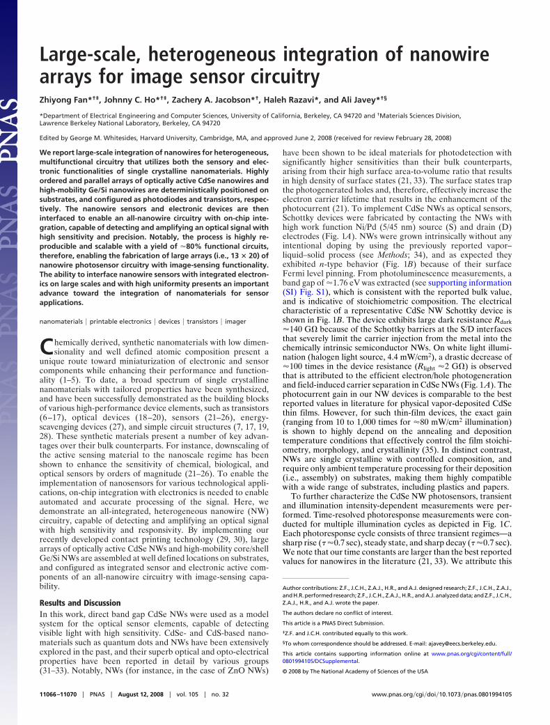
Although the miniaturized nanosensor elements, such as theCdSe NW photodetectors shown here, provide high sensitivity tothe environment with high spatial resolution, they are inherentlylimited to low signal amplitude (i.e., current), and thereforerequire an eventual signal amplification via electronic circuitryto enable effective data processing. To date, this importantrequirement has not yet been addressed. Here, we report direct,on-chip amplification of the nanosensor signal by using anall-NW circuitry without any external wiring. The schematic,SEM, and optical images of a fabricated all-nanowire circuit isshown in Fig. 2, consisting of three active device elements: (i)optical nanosensors (NSs) based on either a single or parallelarrays of multiple CdSe NWs, (ii) a high-resistance field-effecttransistor (FET) (T1) based on parallel arrays of 1–5 Ge/Sicore/shell NWs, and (iii) a low-resistance buffer FET (T2) withthe channel consisting of parallel arrays of �2,000 NWs. The
all-nanowire circuitry utilizes T1 to match the output impedanceof the NS in a voltage divider configuration. Once the illumi-nation-dependent NS current is translated into potential VG2, theoutput current of T2 is modulated according to its transfercharacteristics, resulting in �5 orders of magnitude amplifica-tion of the NS current signal.
To enable the successful fabrication of the all-integrated,heterogeneous NW circuitry, it is essential to assemble highlyregular NW arrays with high uniformity at well defined locationson the substrate. Recently, we have developed a contact printingtechnology for direct transfer of highly ordered and aligned NWarrays on various receiver substrates with high reproducibilityover large areas (29, 30). In this approach, a dense ‘‘lawn’’ ofsingle crystalline NWs with controlled composition is first grownon a growth substrate by using the vapor–liquid–solid process,followed by the transfer of NWs to a receiver substrate by adirectional sliding. Before the printing process, the receiversubstrate is coated with a photolithographically patterned resistlayer that enables for patterned NW assembly on resist removalin acetone. We incorporated this assembly approach for enablingthe fabrication of the all-nanowire sensor circuitry. First, highlyaligned CdSe and Ge/Si NW arrays were assembled at pre-defined locations on a Si/SiO2 (50 nm, thermally grown) sub-strate by using a two-step printing process (see Methods). Ni/PdS/D electrodes were then patterned on NW arrays followed byatomic layer deposition (ALD) of 8- to 9-nm-thick HfO2 film asthe high-� gate dielectric. Finally, the HfO2 layer was selectivelyetched in hydrofluoric acid at the bonding pads and vias, and thetop gate electrodes (Ni/Pd) were patterned on Ge/Si NWs whilesimultaneously forming the vias between the two metal layers
10-4
10-3
10-2
10-1
100
I DS
(nA)
-10 0 10V
GS (V)
10-3
10-2
10-1
100
I DS (n
A)
-2 -1 0 1 2VDS (V)
B
D1.2
1.0
0.8
0.6
0.4
0.2I D
S (n
A)
12840Intensity (mW/cm2)
D (Ni/Pd)
S (Ni/Pd) A
5µm
C
VDS = 2V
VDS = 2VVDS = 2V
2
46
10-1
2
46
100
I DS (n
A)
2001000Time (sec)
VGS = 0V
Fig. 1. Highly sensitive, direct band-gap NW photodiodes. (A) SEM (Top), schematic (Middle), and the band diagram (Bottom) of a CdSe NW photodetectorwith Ni/Pd Schottky S/D contacts. (B) IDS-VGS and IDS-VDS (Inset) curves of a representative CdSe NW device before (dashed, gray line) and after (solid, red line) whitelight illumination, exhibiting �100 times the current modulation. (C) Transient of a single CdSe NW device with an illumination intensity of 4.4 mW/cm2. (D)Illumination intensity-dependent measurements of a CdSe NW device, showing a nonlinear behavior.
Fan et al. PNAS � August 12, 2008 � vol. 105 � no. 32 � 11067
ENG
INEE
RIN
G
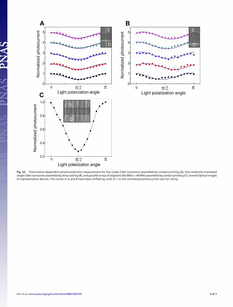
(see Methods). Fig. 2C shows an optical microscopy image of afabricated circuit and scanning electron microscopy (SEM)images of each individual component, clearly demonstrating thehighly ordered NW positioning and the on-chip integration. Theachieved NW alignment is highly desirable for high-performanceand highly uniform transistor and sensor arrays. For transistors,a high degree of alignment, without NW crossing, is needed toreduce variation in gate electrostatics coupling and NW channellength, both of which directly affect the switching performance.Similarly, for CdSe optical sensors, the alignment is critical foruniform response of the devices, but also more uniquely toenable well defined polarized sensitivity that arises from the 1Dnature of NWs (18). The polarization-dependent photoconduc-tion measurements of single and parallel arrays of CdSe NWs aredepicted in Fig. S2. In particular, near-identical polarization-dependent response is observed for various printed CdSe NWswith similar minima and maxima polarization angles, whichfurther illustrates the highly aligned assembly of NWs by contactprinting. This is in distinct contrast to the randomly aligned NWsassembled by the drop-casting method that show differentpolarized response depending on the orientation of the partic-ular wire.
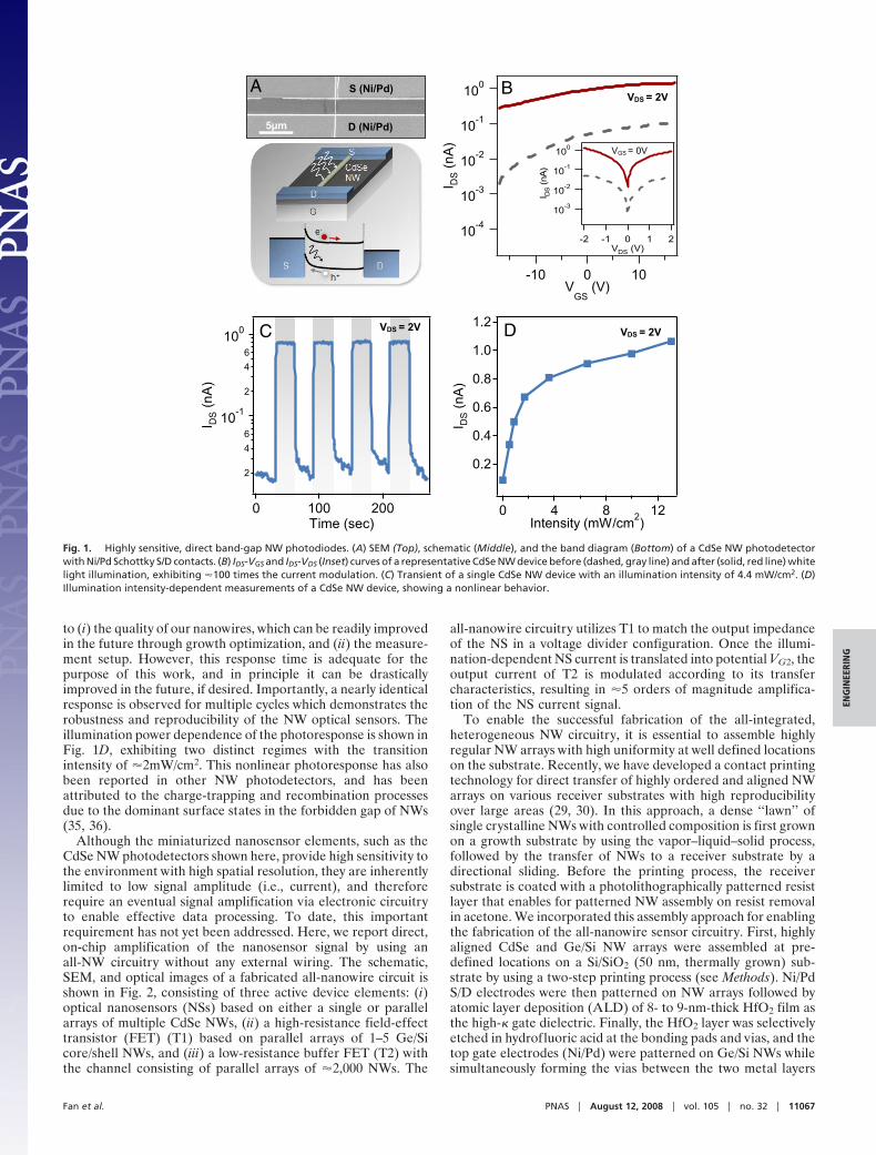
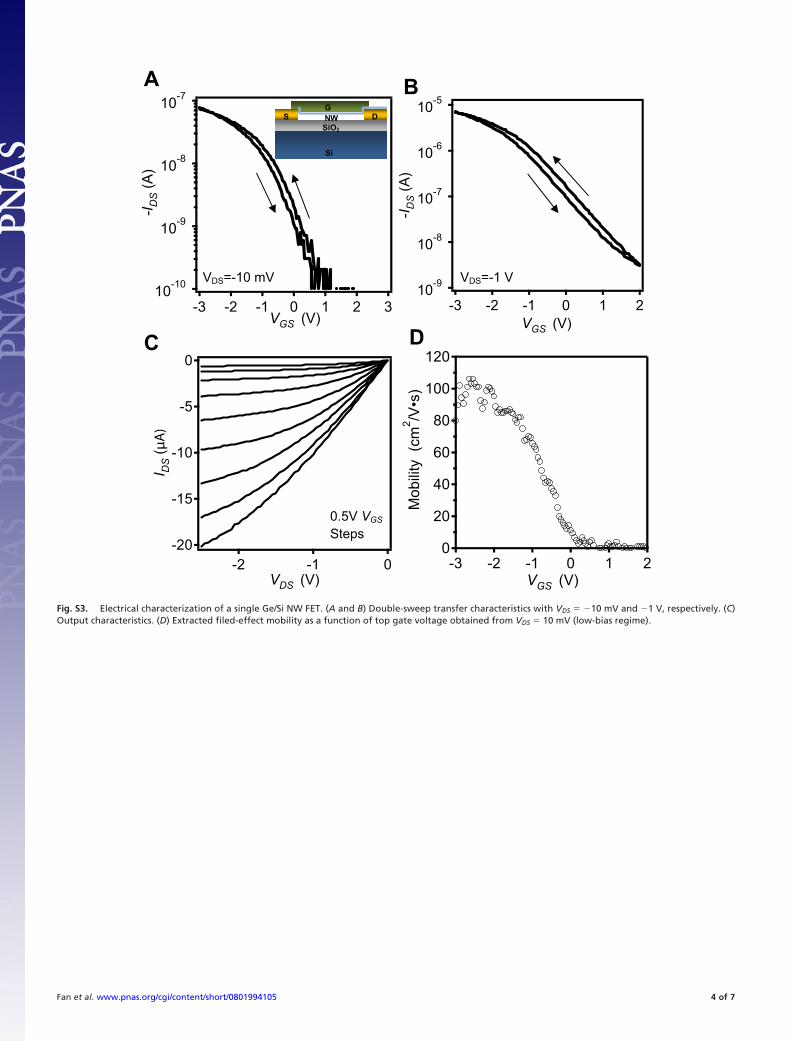
The all-nanowire photosensor circuits were measured at boththe single-device component and circuit levels to characterizetheir operational performance. Fig. 3A shows the transfer char-acteristics of T1 and T2, both exhibiting clear p-type switchingcharacteristics with ION �4 �A and 1 mA, respectively. Furtherdetailed characterization of representative Ge/Si NWs FETs ispresented in Fig. S3. In summary, the Ge/Si NW FETs showedminimal hysteresis (�200 mV) owing to the passivation from theenvironment (i.e., humidity) by the top gate stacks, and thehigh-quality gate dielectrics deposited by ALD (38). A holemobility range of �p � 30–120 cm2/V�s is extracted from thestandard square law model (Fig. S3D). Although the highest �pof our NWs is comparable to that of Si p-metal oxide semicon-ductor FETs, the mobility is �7 times lower than the bestreported value for Ge/Si NW FETs (9, 37). We attribute this tothe nonideal high-�/NW interfaces and/or non-ohmic metalcontacts in our fabricated device structures.
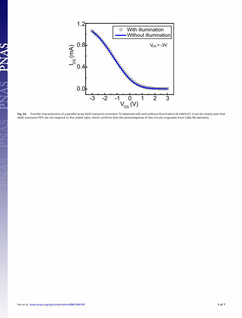
Ge/Si NW FETs were found nonresponsive to white lightillumination which guaranteed no undesired interference (seeFig. S4). For the circuit level operation, the operating bias, VDDwas maintained at �3V for all measurements. The gate electrode
B
C3
4µm
C1
C4
C2
T2 T1
NS
100 µmT1
T2
NS
A
4µm10µm
Fig. 2. Heterogeneous NW assembly for an all integrated, sensor circuitry.(A) Circuit diagram for the all-nanowire photodetector, with high-mobilityGe/Si NW FETs (T1 and T2) amplifying the photoresponse of a CdSe nanosen-sor. (B) Schematic of the all-nanowire optical sensor circuit based on orderedarrays of Ge/Si and CdSe NWs. (C1) An optical image of the fabricated NWcircuitry, consisting of a CdSe nanosensor [NS (C2)] and two Ge/Si core/shell NWFETs [T2 and T1, (C3) and (C4)] with channel widths �300 �m and 1 �m,respectively. Each device element within the circuit can be independentlyaddressed for dynamics studies and circuit debugging.
300
200
100
I out (
µA)
1050Intensity (mW/cm2)
10-3
10-2
10-1
100
I DS (m
A)
20-2VGS (V)
10-5
10-4
10-3
B
C
AT2
T1
300
200
100
-Iou
t (µA
)
3002001000Time (sec)
-1.5
-1.0
-0.5
0.0
VG
2 (V)
Fig. 3. All-integrated NW sensor circuitry. (A) Transfer characteristics ofparallel array Ge/Si NW FETs with channel width of �1 �m (dashed line, T1)and �300 �m (solid line, T2) with VDS � 3V. The blue box represents the activeoperation regime in which the photosensor circuit is being operated. (B)Circuit output current (blue curve) and voltage divider output voltage (graycurve) response to light illumination (4.4 mW/cm2). (C) Light-intensity-dependent measurement of the circuit output current.
11068 � www.pnas.org�cgi�doi�10.1073�pnas.0801994105 Fan et al.
for T1 was biased at VG1 � 3V (corresponding to RT1 � 1–2 G�)to match the output impedance of the CdSe NS. The outputsignal of a circuit for multiple white light illumination cycles (4.4mW/cm2) is depicted in Fig. 3B, showing average dark and lightcurrents of �80 �A and �300 �A, respectively. Importantly, thisoutput current is quantitatively consistent with the value that isestimated based on the circuit layout and the electrical propertiesof the single-device components. The output current of thecircuit can be estimated from the transfer characteristics of T2and the output voltage of the voltage divider, which is also theinput to T2. The output of the voltage divider, VG2 can beestimated as VG2 � VDD � RT1/(RT1 � RNS), corresponding toV
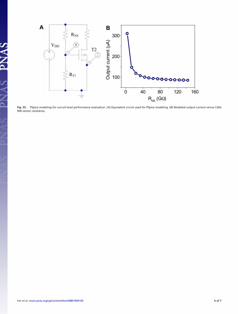
G2 � �0.02V and �1.11V for dark and light (RNS-dark �140 G�and RNS-light �2 G�; Fig. 1B) scenarios, respectively, which is ingood agreement with the measurements (blue curve, Fig. 3B).The VG2 swing defines the operation regime of T2 as depicted inthe transfer characteristics (Fig. 3A). This operation regimecorresponds to an output current swing of 87–310 �A, consistentwith the measured values and the PSpice modeling (see Fig. S5).
The intensity-dependent photoresponse measurements wereconducted as shown in Fig. 3C to further characterize theintegrated circuits. The trend is nearly identical to the photore-sponse of the single CdSe NW device (Fig. 1D), suggesting thatthe signal amplification by the circuit is nearly linear for theillumination intensity of 0–13 mW/cm2. The circuit level mea-surements demonstrate the successful operation of NW circuitsfor effective amplification of the small photocurrent generatedby the NS elements.
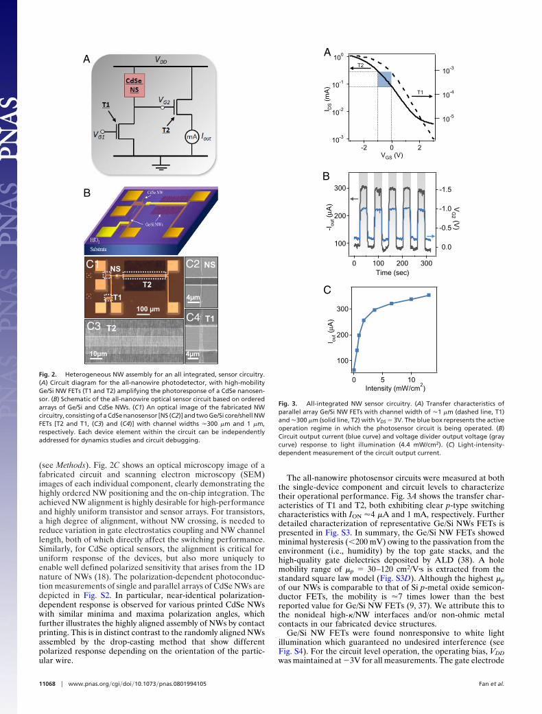
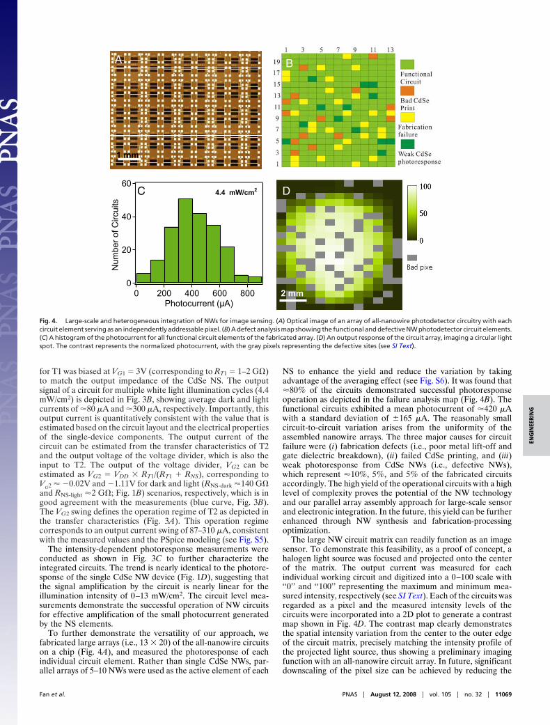
To further demonstrate the versatility of our approach, wefabricated large arrays (i.e., 13 � 20) of the all-nanowire circuitson a chip (Fig. 4A), and measured the photoresponse of eachindividual circuit element. Rather than single CdSe NWs, par-allel arrays of 5–10 NWs were used as the active element of each
NS to enhance the yield and reduce the variation by takingadvantage of the averaging effect (see Fig. S6). It was found that�80% of the circuits demonstrated successful photoresponseoperation as depicted in the failure analysis map (Fig. 4B). Thefunctional circuits exhibited a mean photocurrent of �420 �Awith a standard deviation of �165 �A. The reasonably smallcircuit-to-circuit variation arises from the uniformity of theassembled nanowire arrays. The three major causes for circuitfailure were (i) fabrication defects (i.e., poor metal lift-off andgate dielectric breakdown), (ii) failed CdSe printing, and (iii)weak photoresponse from CdSe NWs (i.e., defective NWs),which represent �10%, 5%, and 5% of the fabricated circuitsaccordingly. The high yield of the operational circuits with a highlevel of complexity proves the potential of the NW technologyand our parallel array assembly approach for large-scale sensorand electronic integration. In the future, this yield can be furtherenhanced through NW synthesis and fabrication-processingoptimization.
The large NW circuit matrix can readily function as an imagesensor. To demonstrate this feasibility, as a proof of concept, ahalogen light source was focused and projected onto the centerof the matrix. The output current was measured for eachindividual working circuit and digitized into a 0–100 scale with‘‘0’’ and ‘‘100’’ representing the maximum and minimum mea-sured intensity, respectively (see SI Text). Each of the circuits wasregarded as a pixel and the measured intensity levels of thecircuits were incorporated into a 2D plot to generate a contrastmap shown in Fig. 4D. The contrast map clearly demonstratesthe spatial intensity variation from the center to the outer edgeof the circuit matrix, precisely matching the intensity profile ofthe projected light source, thus showing a preliminary imagingfunction with an all-nanowire circuit array. In future, significantdownscaling of the pixel size can be achieved by reducing the
60
40
20
0
Num
ber o
f Circ
uits
8006004002000Photocurrent (µA)
DC
A
2 mm
B
1 mm
4.4 mW/cm2
Fig. 4. Large-scale and heterogeneous integration of NWs for image sensing. (A) Optical image of an array of all-nanowire photodetector circuitry with eachcircuit element serving as an independently addressable pixel. (B) A defect analysis map showing the functional and defective NW photodetector circuit elements.(C) A histogram of the photocurrent for all functional circuit elements of the fabricated array. (D) An output response of the circuit array, imaging a circular lightspot. The contrast represents the normalized photocurrent, with the gray pixels representing the defective sites (see SI Text).
Fan et al. PNAS � August 12, 2008 � vol. 105 � no. 32 � 11069
ENG
INEE
RIN
G
feature size (for instance, channel length and width) of the Ge/SiNW FETs and the metal interconnects.
In summary, the large-scale assembly of NWs for heteroge-neous, sensor circuitry with on-chip integration was demon-strated. The sensory and electronic functionalities of NWs havebeen interfaced through heterogeneous integration of directband gap CdSe NWs and high-mobility Ge/Si NWs. Activeelements consisting of both single and parallel arrays of NWswere incorporated to enable the circuit operation, involving 5orders of magnitude current amplification of the nanosensor’ssignal. Importantly, by using parallel arrays of NWs as the activecomponent of each device, the reliability and uniformity wassignificantly enhanced, therefore, enabling a reliable large-scaleintegration path for the demonstration of an image sensor. In thefuture, the process can be expanded to other optically activeNWs, which combined with the scaling of the fabricated devicesmay enable high-resolution and multicolor imaging. This worknot only demonstrates the nanowire device integration at anunprecedented scale, but also illustrates and presents a systembased on printed NW arrays that may enable a number oftechnological applications by using NWs as the building blocks.
MethodsNanowire Growth. Ge/Si core/shell NW growth process can be found in ref. 9.CdSe nanowires were grown in a custom-made CVD system with a single zone,resistive heating furnace (Lindburg Blue), which accommodates one-inchdiameter quartz tubes. Gold nanoparticles with 30-nm diameter were depos-ited on Si/SiO2 substrates and served as catalysts for the vapor–liquid–solidgrowth process. Before the growth, 1.5 g of CdSe powder (Alfa Aesar,99.999%) was placed in a quartz boat and loaded into the center of theheating zone in the furnace. Then, the growth substrate was placed at thedownstream, �9.5 cm away from the center of the furnace. The nanowiregrowth was carried out with the furnace temperature (precursor tempera-
ture) at 700°C and 50 standard cubic centimeters per minute continuous flowof hydrogen. The system pressure was stabilized at 30 torr with a pressurecontroller and the growth was carried out for 1.5 h.
Nanowire Contact Printing. An alignment mark layer was first created on aSi/SiO2 substrate. Then a layer of photoresist (Shipley 1805 diluted in pro-pylene glycol monomethyl ether acetate with 1:3 volume ratio) was spin-coated on the substrate, and lithographically patterned to define printingchannels for the CdSe nanowire assembly. The details of the printing processcan be found in ref. 29. After CdSe nanowire printing, the photoresist wasremoved in acetone followed by a second printing step for Ge/Si nanowires byusing an identical process flow.
Device Fabrication. After contact printing of CdSe and Ge/Si nanowires, source-drain contact electrodes were patterned with photolithography. Then Ni (5nm)/Pd (45 nm) was evaporated with an electron beam evaporator followedby lift-off. HfO2 high-� gate dielectric film was then deposited by using anatomic layer deposition tool. In this process, tetrakis(dimethylamino) hafniummaintained at 110°C and water were used as the precursors. HfO2 was depos-ited for 85 cycles (�9 nm thick) at 140°C, with each cycle consisting of a 1-sectetrakis(dimethylamino) hafnium precursor pulse, 20-sec nitrogen purge,1-sec water vapor pulse, and 40-sec nitrogen purge. Thereafter, etchingwindows on source-drain bonding pads and the bridges (vias) between theGe/Si transistors were photolithographically patterned, and the HfO2 waschemically etched with 5% HF for 35 sec. Finally, Ni (5 nm)/Pd (45 nm) for thetop metal gate electrodes of T1 and T2, and the vias were fabricated byphotolithography, metallization, and lift-off.
ACKNOWLEDGMENTS. We thank A. M. Peczalski for insightful discussions,and Professor M. Wu and Dr. K. Yu for help with optical measurements. Allfabrication was performed in the Berkeley Microfabrication Laboratory. Thiswork was supported by Defense Advanced Research Projects Agency/Microsystems Technology Office, Intel, and Materials Structures and DeviceFocus Center. The nanowire synthesis was supported by a Laboratory DirectedResearch and Development Project from Lawrence Berkeley National Labo-ratory. J.C.H received a graduate fellowship from Intel Foundation.
1. Lieber CM, Wang ZL (2007) Functional nanowires. MRS Bull 32:99–108.2. Lieber CM (2003) Nanoscale science and technology: Building a big future from small
things. MRS Bull 28:486–491.3. Avouris, P. Chen J (2006) Nanotube electronics and optoelectronics. Mater Today
9:46–54.4. McEuen PL (2000) Single-wall carbon nanotubes. Phys World 13:31–36.5. Rogers JA (2007) Slice and dice, peel and stick: Emerging methods for nanostructure
fabrication. ACS Nano 1:151–153.6. Bryllert T, Wernersson LE, Froberg LE, Samuelson L (2006) Vertical high-mobility
wrap-gated InAs nanowire transistor. IEEE Electron Device Lett 27:323–325.7. Javey A, Nam S, Friendman RS, Yan H, Lieber CM (2007) Layer-by-layer assembly of
nanowires for three-dimensional, multifunctional electronics. Nano Lett 7:773–777.8. Javey A, Guo J, Wang Q, Lundstrom M, Dai HJ (2003) Ballistic carbon nanotube
transistors. Nature 424:654–657.9. Xiang J, et al. (2006) Ge/Si nanowire heterostructures on high-performance field-effect
transistors. Nature 441:489–493.10. Ahn, J. H., et al. (2006) Heterogeneous three-dimensional electronics by use of printed
semiconductor nanomaterials. Science 314:1754–1757.11. Chen ZH, et al. (2006) An integrated logic circuit assembled on a single carbon
nanotube. Science 311:1735.12. Kang SJ, et al. (2007) Printed multilayer superstructures of aligned single-walled
carbon nanotubes for electronic applications. Nano Lett 7:3343–3348.13. Kang SJ, et al. (2007) High-performance electronics using dense, perfectly aligned
arrays of single-walled carbon nanotubes. Nature Nanotech 2:230–236.14. Bachtold A, Hadley P, Nakanishi T, Dekker C (2001) Logic circuits with carbon nanotube
transistors. Science 294:1317–1320.15. Wang D, Sheriff B, Heath JR (2006) Complementary symmetry silicon nanowire logic:
Power-efficient inverters with gain. Small 2:1153–1158.16. Ju S, et al. (2007) Fabrication of fully transparent nanowire transistors for transparent
and flexible electronics. Nat Nanotech 2:378–384.17. Friedman RS, McAlpine MC, Ricketts DS, Ham D, Lieber CM (2005) High-speed inte-
grated nanowire circuits. Nature 434:1085.18. Wang J, Gudiksen MS, Duan X, Cui Y, Lieber CM (2001) Highly polarized photolumi-
nescence and photodetection from single indium phosphide nanowires. Science293:1455–1457.
19. Tian B, et al. (2007) Coaxial silicon nanowires as solar cells and nanoelectronic powersources. Nature 449:885–889.
20. Lewis NS (2007) Toward cost-effective solar energy use. Science 315:798–801.
21. Soci C, et al. (2007) ZnO nanowire UV photodetectors with high internal gain. NanoLett 7:1003–1009.
22. Cui Y, Wei Q, Park H, Lieber CM (2001) Nanowire nanosensors for highly sensitive andselective detection of biological and chemical species. Science 293:1289–1292.
23. Patolsky F, et al. (2006) Detection, stimulation, and inhibition of neuronal signals withhigh-density nanowire transistor arrays. Science 313:1100–1104.
24. McAlpine MC, Ahmad H, Wang D, Heath JR (2007) Highly ordered nanowire arrays onplastic substrates for ultrasensitive flexible chemical sensors. Nat Mater 6:379–384.
25. Zhang DH, et al. (2004) Detection of NO2 down to ppb levels using individual andmultiple In2O3 nanowire devices. Nano Lett 4:1919–1924.
26. Stern E, et al. (2007) Label-free immunodetection with CMOS-compatible semicon-ducting nanowires. Nature 445:519–522.
27. Wang ZL, Song J (2006) Piezoelectric nanogenerators based on zinc oxide nanowirearrays. Science 312:242–246.
28. Ju S, et al. (2008) Transparent active matrix organic light-emitting diode displays drivenby nanowire transistor circuitry. Nano Lett 8:997–1004.
29. Fan Z, et al. (2008) Wafer-scale assembly of highly ordered semiconductor nanowirearrays by contact printing. Nano Lett 8:20–25.
30. Yerushalmi R, Jacobson ZA, Ho JC, Fan Z, Javey A (2007) Large scale, highly orderedassembly of nanowire parallel arrays by differential roll printing. Appl Phys Lett91:203104.
31. Chan EM, Mathies RA, Alivisatos AP (2003) Size-controlled growth of CdSe nanocrystalsin microfluidic reactors. Nano Lett 3:199–201.
32. Gudiksen MS, Maher KN, Ouyang L, Park H (2005) Electroluminescence from a single-nanocrystal transistor. Nano Lett 5:2257–2261.
33. Jie JS, et al. (2006) Photoconductive characteristics of single-crystal CdS nanoribbons.Nano Lett 6:1887–1892.
34. Ma C, Wang ZL (2005) Road map for the controlled synthesis of cdse nanowires, nanobelts,and nanosaws—A step towards nanomanufacturing. Adv Mater 17:2635–2639.
35. Raturi AK, Thankaraj R, Sharma AK, Tripathi BB, Agnihotri OP (1982) Structural, optical,and photoconducting properties of sprayed CdSe Films. Thin Solid Films 91:55–64.
36. Rose A (1963) Concepts in Photoconductivity and Allied Problems (Interscience, NewYork).
37. Hu Y, Xiang J, Liang G, Yan H, Lieber CM (2008) Sub-100 nanometer channel lengthGe/Si nanowire transistors with potential for 2 THz switching speed. Nano Lett 8:925–930.
38. Javey A, et al. (2002) High-k dielectrics for advanced carbon nanotube transistors andlogic. Nat Mater 1:241–246.
11070 � www.pnas.org�cgi�doi�10.1073�pnas.0801994105 Fan et al.
Supporting InformationFan et al. 10.1073/pnas.0801994105SI TextPolarization-Dependent Photoconduction. Because of the 1D fea-ture of semiconductor nanowires, they demonstrate uniquepolarized photoconduction properties as reported for single NWdevices (1). In this work, polarization-dependent photoconduc-tion was measured for contact-printed (highly aligned) anddrop-casted (random orientation) CdSe nanowires in both singleNW and parallel array configurations. A randomly polarized 10mW He-Ne (� � 633 nm) laser was used as the light source inconjunction with a linear polarizer. By rotating the polarizer, thepolarization angle of the incident light was tuned from 0 to 180°with respect to the edge of the source/drain electrodes. Sup-porting information (SI) Fig. S2 A and B shows the polarizedphotoconduction of single CdSe NW devices made by contactprinting and drop casting of NWs, respectively. Although thecontact-printed NW devices exhibit near-identical response withthe photocurrent minimum at 90° and maxima at 0 and 180°polarization (angle in respect to the normal of S/D electrodes),the drop-casted (random orientation) NW devices exhibit anonuniform response with a large device-to-device variation intheir minima and maxima polarization angles. This result illus-trates the highly oriented nanowire assembly achieved by thecontact-printing process, in clear contrast to the random align-ment obtained from drop casting of nanowires on substrates.Furthermore, polarized photoconduction measurements wereconducted on parallel arrays of nanowires assembled by contactprinting. As shown in Fig. S2C, the devices exhibit a minimumphotocurrent at 90° and maxima at 0 and 180°, once againillustrating the high degree of alignment attained by the contactprinting process.
Electrical Characterization of Ge/Si NW FETs. Low- and high-biastransfer characteristics of a single Ge/Si NW FET (top gated, 8–9nm HfO2 gate dielectric, d � 30 nm, L �3 �m) is shown in Fig.S3 A and B for backward and forward gate voltage-sweepingdirections. The transistors exhibit minimal hysteresis. From thetransfer characteristics, the field-effect mobility of holes wasobtained by using the square law model. The gate capacitance,C � 3.2 � 10�15 F, was obtained from simulation by using version4.0.1 of Finite Element Method Magnetics software. In thelow-bias linear-triode region (i.e., VDS � 10 mV) the holemobility, �h can be deduced from
�h �gmL2
VDSC,
where gm is the transconductance, gm � dI/dVGS�VDS. A plot of
mobility as a function of gate voltage is shown in Fig. S3D,illustrating a peak mobility of �100 cm2/V�s for this device. Themobility range for the studied NW devices was 30–120 cm2/V�swith a peak transconductance range (normalized by diameter) of100–400 S/m. In the future, key transistor metrics, such astransconductance, can be improved by downscaling of the chan-nel length and gate dielectric thickness (2–4).
SPICE Modeling. After single-device component measurements,Pspice (OrCAD Version 9.1) modeling was carried out tosimulate the circuit output performance (Fig. S5). The simula-tion used the previously mentioned values (in the text) forresistance of NS and T1. For T2, PMOS model 1 was used withKp � 1.235 � 10�4 F�cm�2�(V�s)�1 and VT � 1.13 V. Thesimulation output is shown in Fig. S5B. Interestingly, the simu-lation results match well with the experimental data.
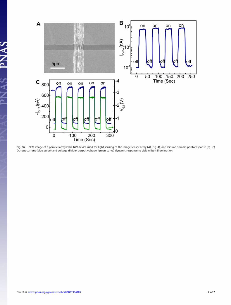
Sensor Circuitry with Parallel Arrays of CdSe NWs. To improve theuniformity, parallel arrays of CdSe NWs (5–10 NWs) wereprinted as light sensor elements for the large matrix fabricationas shown in Fig. S6A. Fig. S6B represents the time domainphotoresponse of the CdSe NWs, demonstrating �100 pA darkcurrent and �8 nA photocurrent with an illumination intensityof 4.4 mW/cm2 and VDS � 3V. The output current of the circuitis shown in Fig. S6C, showing �5 orders of magnitude currentamplification by the all-NW circuitry.
Image Construction with Sensor Circuit Array. To demonstrate theimage-sensing function with the nanowire circuit array, a halo-gen light spot (diameter: �6 mm, peak intensity at the center: �4mW/cm2) from a microscope on the probe station was projectedat the center of the circuit array and the current output (Iout)from each circuit was measured pixel by pixel.
The measured current from each circuit pixel was digitized toan integer (Z) between 0 and 100 according the followingequation:
Z � Integer�100�Iout�Imin
Imax�Imin�
where Imax and Imin correspond to the light current at 4 mW/cm2
illumination and the dark current, respectively, which weremeasured for each circuit during a calibration step before theimage-sensing experiment. Eventually, a 13 � 20 intensity matrixwas formed from the Z values with each circuit corresponding toa single pixel (Fig. 4D).
1. Wang J, Gudiksen MS, Duan X, Cui Y, Lieber CM (2001) Highly polarized photolumi-nescence and photodetection from single indium phosphide nanowires. Science293:1455–1457.
2. Xiang J, et al. (2006) Ge/Si nanowire heterostructures on high-performance field-effecttransistors. Nature 441:489–493.
3. Hu Y, Xiang J, Liang G, Yan H, Lieber CM (2008) Sub-100 nanometer channel lengthGe/Si nanowire transistors with potential for 2 THz switching speed. Nano Lett 8:925–930.
4. Javey A, et al. (2002) High-k dielectrics for advanced carbon nanotube transistors andlogic. Nat Mater 1:241–246.
Fan et al. www.pnas.org/cgi/content/short/0801994105 1 of 7
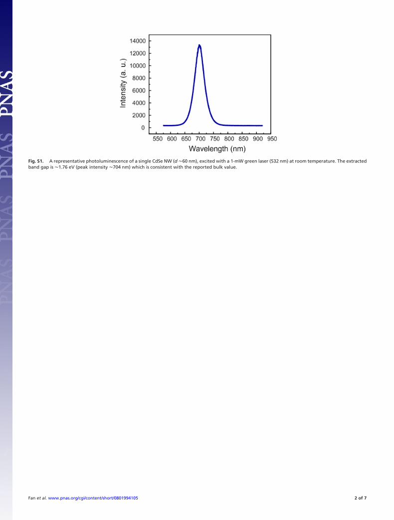
Fig. S1. A representative photoluminescence of a single CdSe NW (d �60 nm), excited with a 1-mW green laser (532 nm) at room temperature. The extractedband gap is �1.76 eV (peak intensity �704 nm) which is consistent with the reported bulk value.
Fan et al. www.pnas.org/cgi/content/short/0801994105 2 of 7
A B
C
S
D
S
D
S
D
Fig. S2. Polarization-dependent photoconduction measurement for five single CdSe nanowires assembled by contact printing (A), five randomly orientatedsingle CdSe nanowires assembled by drop casting (B), and parallel arrays of aligned CdSe NWs (�40 NW) assembled by contact printing (C). (Insets) Optical imagesof representative devices. The curves in A and B have been shifted by units of 1 in the normalized photocurrent axis for clarity.
Fan et al. www.pnas.org/cgi/content/short/0801994105 3 of 7
10-10
10-9
10-8
10-7
-I D
S (A
)
-3 -2 -1 0 1 2 3VGS (V)
-20
-15
-10
-5
0
ID
S (μ
Α)
-2 -1 0VDS (V)
10-9
10-8
10-7
10-6
10-5
-I DS (A
)
-3 -2 -1 0 1 2VGS (V)
120
100
80
60
40
20
0
Mob
ility
(cm
2 /V•s
)
-3 -2 -1 0 1 2VGS (V)
S DNW G
SiO2
Si
VDS VVm01-= DS=-1 V
0.5V VGS
Steps
C D
A B
Fig. S3. Electrical characterization of a single Ge/Si NW FET. (A and B) Double-sweep transfer characteristics with VDS � �10 mV and �1 V, respectively. (C)Output characteristics. (D) Extracted filed-effect mobility as a function of top gate voltage obtained from VDS � 10 mV (low-bias regime).
Fan et al. www.pnas.org/cgi/content/short/0801994105 4 of 7
1.2
-3 -2 -1 0 1 2 30.0
0.4
0.8
VGS (V)
I DS (
mA
)
With illumination Without illumination
VDS = -3V
Fig. S4. Transfer characteristics of a parallel array Ge/Si nanowire transistor T2 obtained with and without illumination (4 mW/cm2). It can be clearly seen thatGe/Si nanowire FETs do not respond to the visible light, which confirms that the photoresponse of the circuits originates from CdSe NS elements.
Fan et al. www.pnas.org/cgi/content/short/0801994105 5 of 7
0 40 80 120 160
100
200
300
Out
put c
urre
nt (μ
A)
RNS (GΩ)
A B
VDD
RT1
RNS
T2
Fig. S5. PSpice modeling for curcuit level performance evaluation. (A) Equivalent circuit used for PSpice modeling. (B) Modeled output current versus CdSeNW sensor resistance.
Fan et al. www.pnas.org/cgi/content/short/0801994105 6 of 7
0 50 100 150 200 250
10-1
100
101
Time (Sec)
I CdS
e (nA
)
ononon
offoffoffoffoff
onB
0 100 200 300
0
200
400
600
800
0
-1
-2
-3
-4
V G2 (
V)
-I OU
T (μA
)
Time (Sec)
ononononon
offoffoffoffoffoff
C
A
Fig. S6. SEM image of a parallel array CdSe NW device used for light sensing of the image sensor array (A) (Fig. 4), and its time domain photoresponse (B). (C)Output current (blue curve) and voltage divider output voltage (green curve) dynamic response to visible light illumination.
Fan et al. www.pnas.org/cgi/content/short/0801994105 7 of 7