Embed Size (px)
Citation preview

1
Copyright 2004 NMDG Engineering
Large-Signal Network Analysis Technologyfor HF analogue and fast switching components
Applications
This slide set introduces the large-signal network analysis technology applied to high-frequency components. These components can be analogue or digital. Indeed, due to the increased speed of digital signals, it becomes important to treat the digital signals more and more as analogue signals.
In a separate presentation, the theoretical aspects of large-signal network analysis is explained.
In this presentation, some examples are shown to give a flavor of what can be done, once the key information of the nonlinear behavior is measured.

2
2Certain slides are with permission from Agilent Technologies
Copyright 2004 NMDG Engineering
Applications
Transistor reliability Transistor model verification (ICCAP / ADS) Transistor model tuning System level characterization Scattering functions Memory effect Dynamic bias High-Speed digital PA design using waveform engineering Conclusions

3
3Certain slides are with permission from Agilent Technologies
Copyright 2004 NMDG Engineering
Gate-Drain Breakdown Current
Time (ns)
º transistor provided by David Root, Agilent Technologies - MWTC
º TELEMIC / KUL
Investigating transistor reliability under realistic operating conditions is the first application we show.
On the above figures we see the voltage and current time domain waveforms as they appear at the gate and drain of a FET transistor. These measurements were done applying an excitation signal of 1GHz at the gate. The signal amplitude is increased until we see a so-called breakdown current. It shows up as a negative peak (20mA) for the gate current, and as an equal amplitude positive peak at the drain. We actually witness a breakdown current which flows from the drain towards the gate. This kind of operating condition deteriorates the transistor and is a typical cause of transistor failure.
To our knowledge, the above figures show the first measurements ever of breakdown current under large-signal RF excitation.
4
4Certain slides are with permission from Agilent Technologies
Copyright 2004 NMDG Engineering
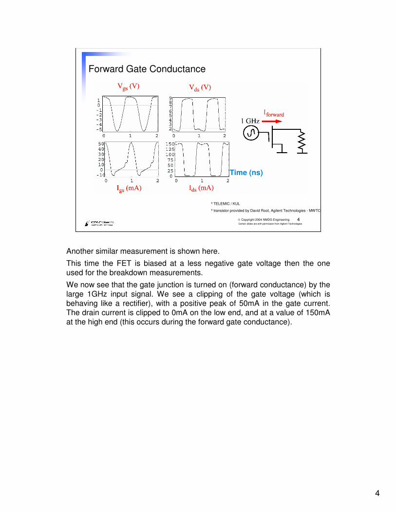
Forward Gate Conductance
Time (ns)
º transistor provided by David Root, Agilent Technologies - MWTC
º TELEMIC / KUL
Another similar measurement is shown here.
This time the FET is biased at a less negative gate voltage then the one used for the breakdown measurements.
We now see that the gate junction is turned on (forward conductance) by the large 1GHz input signal. We see a clipping of the gate voltage (which is behaving like a rectifier), with a positive peak of 50mA in the gate current. The drain current is clipped to 0mA on the low end, and at a value of 150mA at the high end (this occurs during the forward gate conductance).

5
5Certain slides are with permission from Agilent Technologies
Copyright 2004 NMDG Engineering
Applications
Transistor reliability Transistor model verification (ICCAP / ADS) Transistor model tuning PA optimization using Waveform Engineering System level characterization Scattering functions Memory effect Dynamic bias High-Speed digital PA design using waveform engineering Conclusions

6
6Certain slides are with permission from Agilent Technologies
Copyright 2004 NMDG Engineering
Model Verification in CAE tool
MeasuredIncident Waves
50 100 150 200 250
1.5
2
2.5
3
3.5
4
50 100 150 200 250-0.01
0.01
0.02
0.03
0.04
0.05
0.06
50 100 150 200 250
-2
-1.5
-1
-0.5
50 100 150 200 250
-0.01
-0.005
0.005
0.01
-2 -1.5 -1 -0.5
-0.01
-0.005
0.005
0.01
1.5 2 2.5 3 3.5 4-0.01
0.01
0.02
0.03
0.04
0.05
0.06
Model
ADS gi
didv
gi
gvdv
di
Measured and SimulatedVoltages and Currents
Multi-line TRL
gv
It is possible to use the measured incident waves as input to a model that exists in a CAE tool. The scattered waves are then simulated and compared to the measured waves. This allows to identify possible problems with the model. Of course, one should use realistic test signals to check the model “under realistic conditions”.
The picture shows voltage and current at the gate and the drain, both simulated and measured.
Also the dynamic load line is visualized (current versus voltage at the drain) and something similar at the gate (current versus the voltage at the gate).
When the model does not correspond to the measurements, one can consider to tune the model against the large signal measurements.
7
7Certain slides are with permission from Agilent Technologies
Copyright 2004 NMDG Engineering
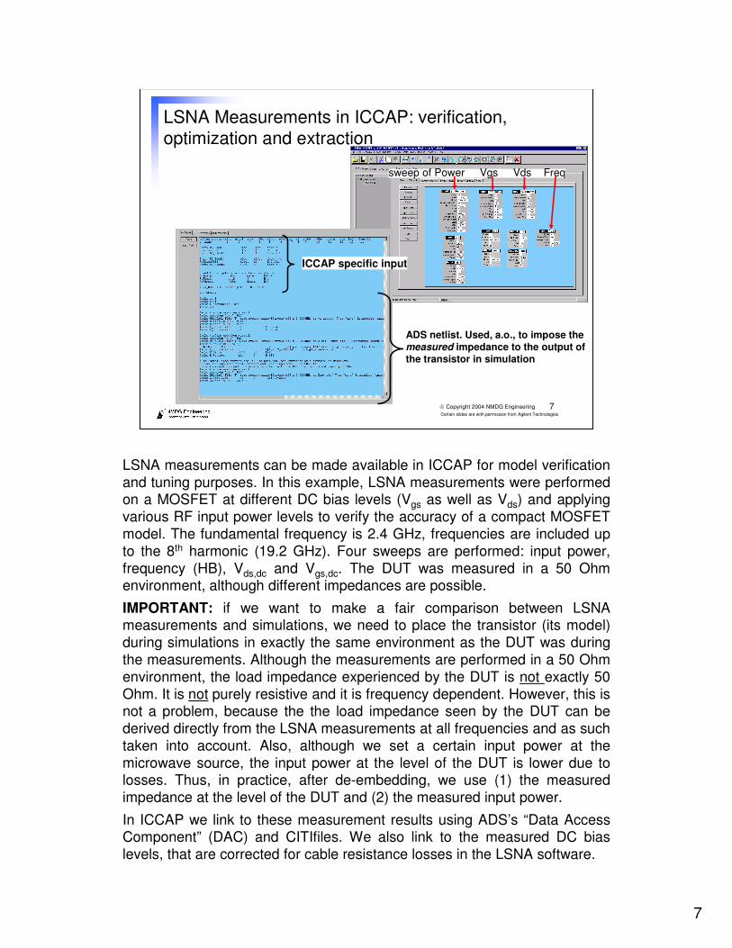
LSNA Measurements in ICCAP: verification, optimization and extraction
ICCAP specific input
ADS netlist. Used, a.o., to impose themeasured impedance to the output ofthe transistor in simulation
sweep of Power Vgs Vds Freq
LSNA measurements can be made available in ICCAP for model verification and tuning purposes. In this example, LSNA measurements were performed on a MOSFET at different DC bias levels (Vgs as well as Vds) and applying various RF input power levels to verify the accuracy of a compact MOSFET model. The fundamental frequency is 2.4 GHz, frequencies are included up to the 8th harmonic (19.2 GHz). Four sweeps are performed: input power, frequency (HB), Vds,dc and Vgs,dc. The DUT was measured in a 50 Ohm environment, although different impedances are possible.
IMPORTANT: if we want to make a fair comparison between LSNA measurements and simulations, we need to place the transistor (its model) during simulations in exactly the same environment as the DUT was during the measurements. Although the measurements are performed in a 50 Ohm environment, the load impedance experienced by the DUT is not exactly 50 Ohm. It is not purely resistive and it is frequency dependent. However, this is not a problem, because the the load impedance seen by the DUT can be derived directly from the LSNA measurements at all frequencies and as such taken into account. Also, although we set a certain input power at the microwave source, the input power at the level of the DUT is lower due to losses. Thus, in practice, after de-embedding, we use (1) the measured impedance at the level of the DUT and (2) the measured input power.
In ICCAP we link to these measurement results using ADS’s “Data Access Component” (DAC) and CITIfiles. We also link to the measured DC bias levels, that are corrected for cable resistance losses in the LSNA software.

8
8Certain slides are with permission from Agilent Technologies
Copyright 2004 NMDG Engineering
Transistor De-embedding
0 0.5 1 1.5 2
3
2
1
0
1
2before
afterde-embedding
Time/period
Gat
e cu
rren
t/ m
A
Equivalent circuit of the RF test-structure, including the DUT andlayout parasitics
The purpose of the de-embedding technique is to shift the calibration reference planes closer to the DUT, in the above case, from the probe tips to the transistor itself.
As such, one has to calculate the values of the 6 unknown parasitic components (between probe tips and transistor) that influence the RF behaviour of the DUT (as shown in the slide) and correct the measurement results accordingly. The admittances G1, G2 and G3 represent the coupling via the metal interconnections and the silicon substrate between the pads of gate (=port1) and source, drain (=port2) and source, and gate and drain, respectively. Z1 and Z2 originate from the metal interconnection series impedances between port 1 and port 2, respectively, on one hand and the actual device-under-test on the other. Z3 represents the ground leads towards the DUT.
Thus, the first step in the large-signal de-embedding is to measure the S-parameters (LSNA used in VNA mode), at the defined frequency grid, of the on-wafer de-embedding structures and convert them to Y-parameters using a conversion table. In our example, we measured the de-embedding structures at f=2.4 GHz, 4.8 GHz, … , 8*2.4=19.2 GHz. Subsequently, the resulting Y-parameters are then used to calculate the parasitic components (G1, G2, G3, Z1, Z2, and Z3 as shown in the slide) at all harmonic frequencies. Knowing these values, the voltages and currents can be calculated at the transistor eliminating the parasitics.

9
9Certain slides are with permission from Agilent Technologies
Copyright 2004 NMDG Engineering
Input capacitance behavior
Vgs,dc=0.9 VVds,dc=0.3 V Vds,dc=1.8 V
Input loci turn clockwise, conform i=C*dv/dt
Let us take a look now at some large-signal measurement and simulation results. The figures show the instantaneous gate current versus the instantaneous gate voltage at different DC bias settings. These, so called, input loci turn clockwise, conform i=C.dv/dt. If the gate capacitance does not depend on the gate voltage, the input locus will be shaped like an ellipse. A distorted ellipse indicates that the gate capacitance depends on the gate voltage, as is the case for a MOSFET. The input locus immediately reveals whether the gate capacitance model is accurate or not. The results presented here indicate that the modelled and measured input loci show similar trends. However, the absolute model accuracy can still be improved by optimizing gate capacitance model parameters towards these measurement results, as will be shown later in this presentation.

10
10Certain slides are with permission from Agilent Technologies
Copyright 2004 NMDG Engineering
Dynamic load line & transfer characteristic
Vgs,dc=0.3 VVds,dc=0.9 V
Other important large-signal characteristics of a DUT are the transfer locus and dynamic loadline. They show the instantaneous output current versus instantaneous input voltage and output voltage, respectively (arrows indicate time progress). Observe that, for this operating condition,, the drain current is negative for a short period of time, due to the direct coupling between gate and drain through the gate-drain capacitances (overlap and fringing). In fact, there is a small current that flows directly from the gate to the drain (i=C*dv/dt, with dv/dt positive) when the gate voltage starts to increase after it has obtained its lowest value. Because the drain current is defined as being positive when flowing into the transistor, during a small period of time a negative drain current can be observed.
The dynamic loadline and transfer locus turn counterclockwise and show hysteresis. The transfer locus clearly shows that the drain current does not follow the gate voltage instantaneously, due to finite charging and discharging times (mainly RC contribution, no contribution of non-quasi static effects yet at these frequencies). The opening of the dynamic loadline largely stems from the complex value of the load impedance as seen by the transistor.

11
11Certain slides are with permission from Agilent Technologies
Copyright 2004 NMDG Engineering
Identifying modeling problems: extrapolation example SiGe HBT ...
SiGe HBT (model parameters extracted using DC measurements up to 1V)Vbe= 0.9 V; Vce=1.5 V; Pin= - 6 dBm; f0= 2.4 GHz
100 200 300 400 500 600 700 8000 900
-0.002
-0.001
0.000
0.001
-0.003
0.002
time, ps
i1st
si1
mts
_de
100 200 300 400 500 600 700 8000 900
0.6
0.7
0.8
0.9
1.0
1.1
0.5
1.2
time, ps
v1st
sv1
mts
_de
100 200 300 400 500 600 700 8000 900
1.3
1.4
1.5
1.6
1.2
1.7
time, ps
v2st
sv2
mts
_de
100 200 300 400 500 600 700 8000 900
0.000
0.002
0.004
0.006
-0.002
0.008
time, ps
i2st
si2
mts
_de
simul.meas.
This slide shows the effect of not taking into account a sufficient range of DC bias levels during the extraction of the model parameters. This example is provided with courtesy of the Alcatel Microelectronics and the Alcatel SEL Stuttgart Research Center teams. In a first step, model parameters for a SiGe HBT technology were extracted using DC bias-levels up to 1 V. However, during LSNA measurements, the maximum instantaneous voltage at port 1 was 1.15 V. These LSNA measurements were performed using realistic operating conditions, i.e. operating conditions that are used by the circuit designers. One clearly sees that the agreement between measured and modeled currents and voltages is far from good. From the simulated data one could, for example, wrongly conclude that the output current clips at high current levels, while this is just due to the limited range of DC bias levels used during model parameter extraction. Of course, there is also a large disagreement in the DC behavior above 1 V, as shown in the next slide. As long as you do not measure the large-signal behavior of your transistor under realistic large-signal RF operating conditions, you will not be able detect these kind of modeling problems.
This example also shows that, during model parameter extraction, it is of paramount importance to consider the area of applications (and the corresponding boundaries), where the transistor will be used.

12
12Certain slides are with permission from Agilent Technologies
Copyright 2004 NMDG Engineering
… Identifying modeling problems: extrapolation example SiGe HBT
Measurement Simulation
SiGe HBT - DC characteristics (different Vce)
0.2 0.4 0.6 0.8 1.0 1.2 1.40.0 1.6
-0.010
-0.005
0.000
0.005
0.010
0.015
0.020
-0.015
0.025
VbDC
DC
mea
s1..I
ce
0.2 0.4 0.6 0.8 1.0 1.2 1.40.0 1.6
-0.010
-0.005
0.000
0.005
0.010
0.015
0.020
-0.015
0.025
VbDC
i2.i
Alcatel Microelectronics and the Alcatel SELStuttgart Research Center teams are acknowledged
for providing these data.
The agreement between measured and modeled DC characteristics of the SiGe HBT is accurate up to 1 V, but becomes worse for voltages larger than 1 V. Of course, this also has significant effects on the large-signal behavior of the DUT, as was shown in the previous slide.
It is by measuring the large-signal behavior of the DUT with the LSNA and looking at the agreement between measured and modeled large-signal characteristics that this modeling issue was triggered. Now that we know the range of voltages that can appear instantaneously at the input of the transistor, we can take this information into account during model parameter extraction and obtain much better agreement between measurements and simulations.

13
13Certain slides are with permission from Agilent Technologies
Copyright 2004 NMDG Engineering
Applications
Transistor reliability Transistor model verification (ICCAP / ADS) Transistor model tuning System level characterization Scattering functions Memory effect Dynamic bias High-Speed digital PA design using waveform engineering Conclusions
14
14Certain slides are with permission from Agilent Technologies
Copyright 2004 NMDG Engineering
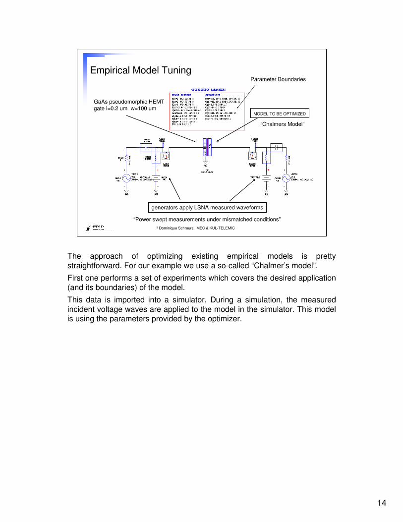
Empirical Model Tuning
MODEL TO BE OPTIMIZED
generators apply LSNA measured waveforms
“Chalmers Model”
“Power swept measurements under mismatched conditions”
GaAs pseudomorphic HEMTgate l=0.2 um w=100 um
Parameter Boundaries
º Dominique Schreurs, IMEC & KUL-TELEMIC
The approach of optimizing existing empirical models is pretty straightforward. For our example we use a so-called “Chalmer’s model”.
First one performs a set of experiments which covers the desired application (and its boundaries) of the model.
This data is imported into a simulator. During a simulation, the measured incident voltage waves are applied to the model in the simulator. This model is using the parameters provided by the optimizer.

15
15Certain slides are with permission from Agilent Technologies
Copyright 2004 NMDG Engineering
Using the Built-in OptimizerDuring OPTIMIZATION
Time domain waveforms Frequency domain
gate drain
voltage
current
gate drain
Voltage - Current State Space
The model parameters are then found by tuning them such that thedifference between the measured and modeled scattered voltage waves is minimized.
Note that one can often use the optimizers of the CAE tool for this purpose.
As with all nonlinear optimizations, it is necessary to have reasonable starting values. For this purpose, one can use the values provided by a simplified version of the classical approaches.
The figures above represent one of the initially modeled and measured gate and drain voltages and currents, and this in the time domain, the frequency domain and in a “current-versus-voltage” representation.
Note especially the large discrepancy between the measured gate current and the one which is calculated by the initial model.

16
16Certain slides are with permission from Agilent Technologies
Copyright 2004 NMDG Engineering
Verification of the Optimized Model
Time domain waveforms Frequency domain
gate drain
voltage
current
gate drain
Voltage - Current State Space
AFTER OPTIMIZATION
The above figures represent the same data after optimization.
Note the very good correspondence that is achieved. This indicates that the model is accurately representing the large-signal behavior for the applied excitation signals.

17
17Certain slides are with permission from Agilent Technologies
Copyright 2004 NMDG Engineering
Waveform Engineering Block Diagram
DUTTestSet
Dat
a-A
cqui
sitio
n
Source
PC
Sampling Converter
Filter
Filter
Filter
Filter
LO
f0
f0
2f0
3f0IRCOM Setup
Waveform engineering corresponds to the synthesis of different source and load conditions to enforce a certain shape of (usually) output voltage and current as a function of time. For example, for an optimal power added efficiency (PAE), one will try to have a low current at a high output voltage and vice versa. This is realized by presenting proper load conditions to a transistor for the different harmonics.
To apply waveform engineering, a large-signal network analyzer must be extended with tuners to control impedances at the different harmonics. In this case active tuners for each harmonic were selected because this allows independent control of the impedances at 3 harmonics. Each loop samples the transmitted wave, changes its amplitude (usually decreases it) and its phase and reinjects it towards the component. In this way, a reflection factor is synthesized which is independent of the transmitted wave.

18
18Certain slides are with permission from Agilent Technologies
Copyright 2004 NMDG Engineering
Example - Measured Waveforms
MesFET Class Ff0=1.8 GHzIds0=7 mAVds0= 6 V
Z(f0)=130+j73 ΩΩΩΩZ(2f0)=1-j2.8 ΩΩΩΩZ(3f0)=20-j97 ΩΩΩΩ
PAE=84%
PAE≈50%
WaveformEngineering
º IRCOM / Limoges
Here the different voltages and currents at the gate and the drain can be observed for different power levels, for a MesFET transistor operating in class F mode. By proper impedance tuning, 84% PAE can be achieved.

19
19Certain slides are with permission from Agilent Technologies
Copyright 2004 NMDG Engineering
Example - Performance ImprovementDerived Information from the V/I waveforms (swept input power at different terminations)
Z(f0)=123+j72 ΩΩΩΩZ(2f0)=50 ΩΩΩΩZ(3f0)=50 ΩΩΩΩ
Z(f0)=123+j72 ΩΩΩΩZ(2f0)=2 - j 4.0 ΩΩΩΩZ(3f0)=50 ΩΩΩΩ
Z(f0)=123+j72 ΩΩΩΩZ(2f0)=2 - j 4.0 ΩΩΩΩZ(3f0)=21-96 ΩΩΩΩ
PAE≈74%
PAE≈74%
PAE≈84%º IRCOM / Limoges
Measuring the voltages and currents at the gate and the drain, allows to derive all other kinds of quantities like output power, PAE, DC power consumption, dissipated power as function of input power and this for different tuner settings. The plots correspond to 3 different load conditions.

20
20Certain slides are with permission from Agilent Technologies
Copyright 2004 NMDG Engineering
Applications
Transistor reliability Transistor model verification (ICCAP / ADS) Transistor model tuning System level characterization Scattering functions Memory effect Dynamic bias High Speed Digital PA design using waveform engineering Conclusions
21
21Certain slides are with permission from Agilent Technologies
Copyright 2004 NMDG Engineering
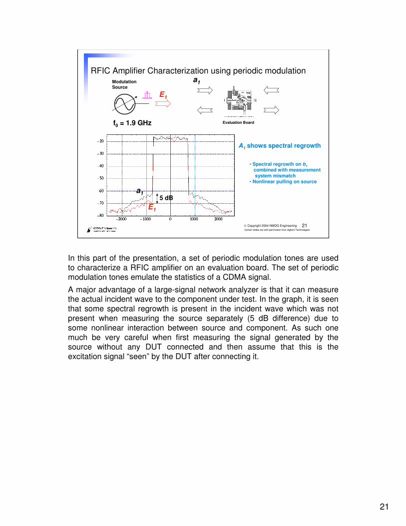
RFIC Amplifier Characterization using periodic modulationModulationSource
a1
E1
a1
E1
A1 shows spectral regrowth
• Spectral regrowth on b1combined with measurementsystem mismatch
• Nonlinear pulling on source
5 dB
f0 = 1.9 GHz Evaluation Board
In this part of the presentation, a set of periodic modulation tones are used to characterize a RFIC amplifier on an evaluation board. The set of periodic modulation tones emulate the statistics of a CDMA signal.
A major advantage of a large-signal network analyzer is that it can measure the actual incident wave to the component under test. In the graph, it is seen that some spectral regrowth is present in the incident wave which was not present when measuring the source separately (5 dB difference) due to some nonlinear interaction between source and component. As such one much be very careful when first measuring the signal generated by the source without any DUT connected and then assume that this is the excitation signal “seen” by the DUT after connecting it.

22
22Certain slides are with permission from Agilent Technologies
Copyright 2004 NMDG Engineering
Transmission Characteristics
A1
Carrier Modulation
Carrier Modulation
B2
Carrier Modulation
3rd harmonicModulation
Harmonic Distortion Compression
The figures represent the incident and transmitted time domain signals as they were measured at the signal ports of a 1.9GHz RFIC amplifier.
The incident signal has characteristics similar to a CDMA signal.
The transmitted signal clearly suffers from compression and harmonic distortion for large instantaneous input amplitudes.
Another way of visualizing this behavior is a so-called “dynamic harmonic distortion” plot.
This is interpreted in exact the same way as a classical harmonic distortion plot, but now the input amplitude does not change step-by-step (using a CW input signal) but changes very fast within the modulation period. The latter may reveal memory effects, as will be explained later.
Note the compression characteristic for the fundamental.

23
23Certain slides are with permission from Agilent Technologies
Copyright 2004 NMDG Engineering
Reflection Characteristics
A1
Carrier Modulation
Carrier Modulation
B1
Carrier Modulation
3rd harmonicModulation
Harmonic Distortion Expansion
2nd harmonicModulation
The figures above represent the incident and reflected time domain voltage waves as they were measured at the input port of a 1.9GHz RFIC amplifier.
The incident signal has characteristics similar to a CDMA signal.
The reflected signal clearly demonstrates expansion and harmonic distortion whenever the input amplitude is high.
Again, another way of visualizing this behavior is a so-called “dynamic harmonic distortion” plot.
Note the expansion characteristic for the fundamental.

24
24Certain slides are with permission from Agilent Technologies
Copyright 2004 NMDG Engineering
Applications
Transistor reliability Transistor model verification (ICCAP / ADS) Transistor model tuning System level characterization Scattering functions Memory effect Dynamic bias High Speed Digital PA design using waveform engineering Conclusions
25
25Certain slides are with permission from Agilent Technologies
Copyright 2004 NMDG Engineering
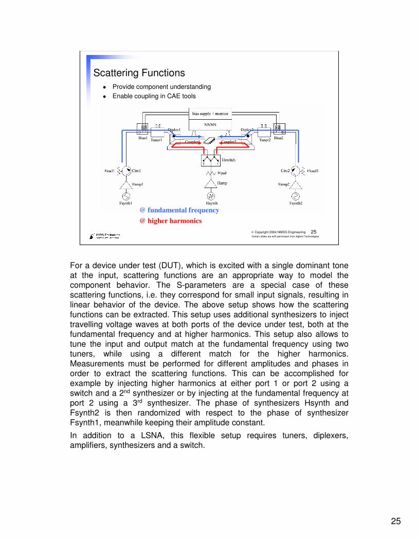
Scattering Functions Provide component understanding Enable coupling in CAE tools
@ fundamental frequency@ higher harmonics
For a device under test (DUT), which is excited with a single dominant tone at the input, scattering functions are an appropriate way to model the component behavior. The S-parameters are a special case of these scattering functions, i.e. they correspond for small input signals, resulting in linear behavior of the device. The above setup shows how the scattering functions can be extracted. This setup uses additional synthesizers to inject travelling voltage waves at both ports of the device under test, both at the fundamental frequency and at higher harmonics. This setup also allows to tune the input and output match at the fundamental frequency using two tuners, while using a different match for the higher harmonics. Measurements must be performed for different amplitudes and phases in order to extract the scattering functions. This can be accomplished for example by injecting higher harmonics at either port 1 or port 2 using a switch and a 2nd synthesizer or by injecting at the fundamental frequency at port 2 using a 3rd synthesizer. The phase of synthesizers Hsynth and Fsynth2 is then randomized with respect to the phase of synthesizer Fsynth1, meanwhile keeping their amplitude constant.
In addition to a LSNA, this flexible setup requires tuners, diplexers, amplifiers, synthesizers and a switch.
26
26Certain slides are with permission from Agilent Technologies
Copyright 2004 NMDG Engineering
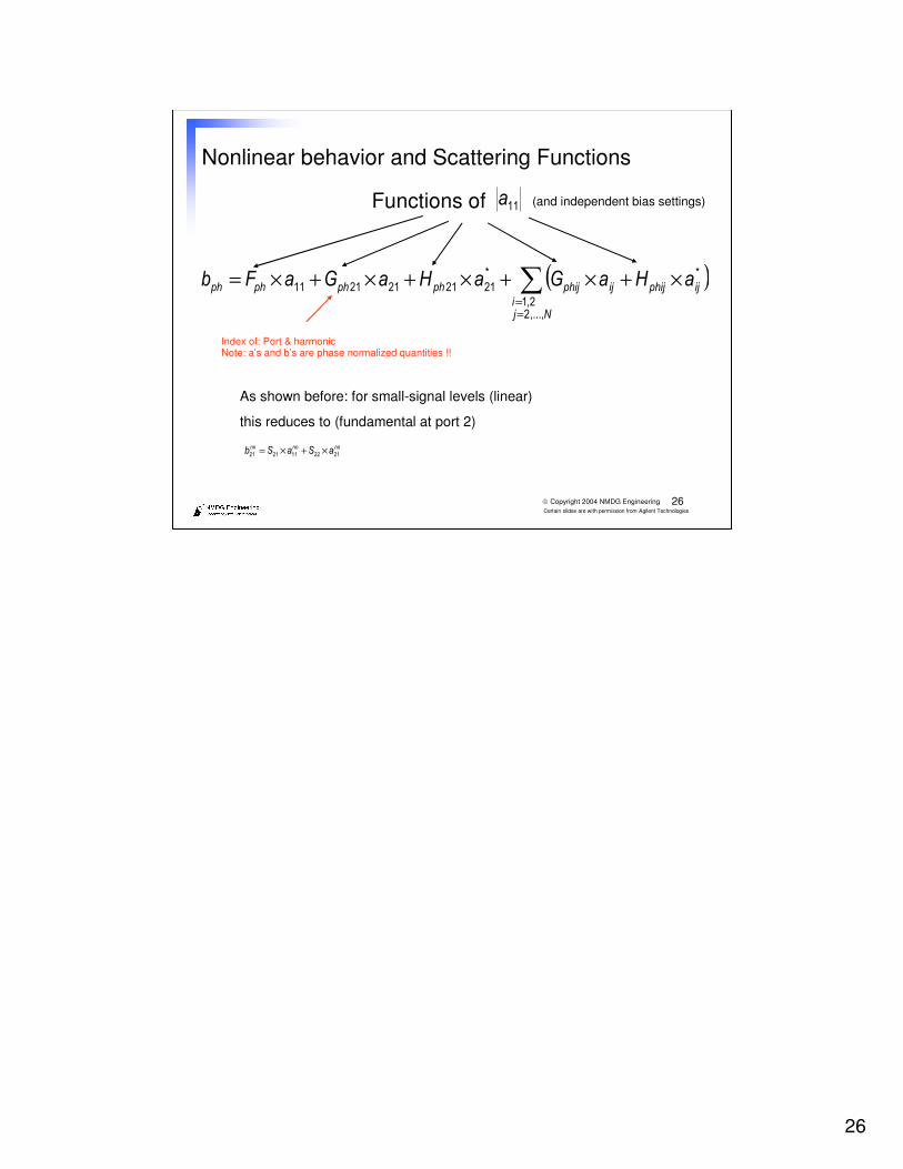
Nonlinear behavior and Scattering Functions
Functions of
Index of: Port & harmonicNote: a’s and b’s are phase normalized quantities !!
As shown before: for small-signal levels (linear)
this reduces to (fundamental at port 2)
×+×=
(and independent bias settings)
( )==
×+×+×+×+×=
27
27Certain slides are with permission from Agilent Technologies
Copyright 2004 NMDG Engineering
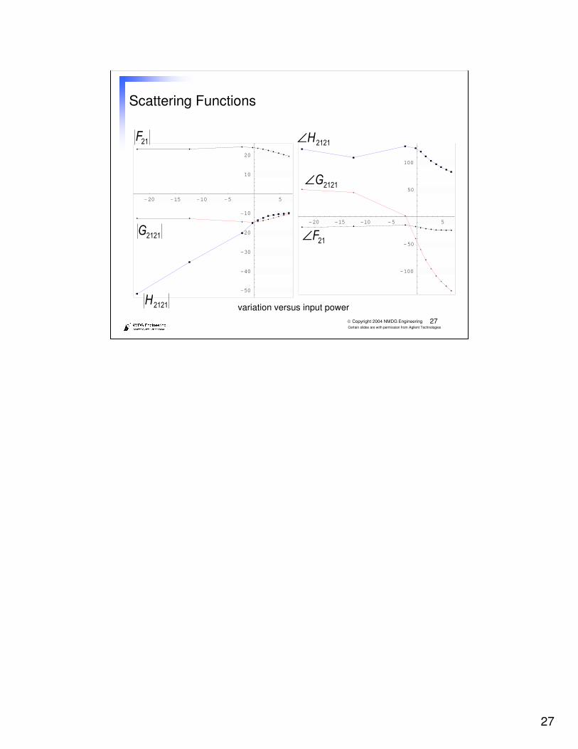
Scattering Functions
20 15 10 5 5
50
40
30
20
10
10
20
20 15 10 5 5
100
50
50
100
∠
∠
∠
variation versus input power

28
28Certain slides are with permission from Agilent Technologies
Copyright 2004 NMDG Engineering
Time domain waveforms
Measured and simulated b-waves
200 400 600 800 1000
0.2
0.1
0.1
0.2
200 400 600 800 1000
6
4
2
2
4
6( )
( )

29
29Certain slides are with permission from Agilent Technologies
Copyright 2004 NMDG Engineering
Applications
Transistor reliability Transistor model verification (ICCAP / ADS) Transistor model tuning System level characterization Scattering functions Memory effect Dynamic bias High Speed Digital PA design using waveform engineering Conclusions

30
30Certain slides are with permission from Agilent Technologies
Copyright 2004 NMDG Engineering
Time domain
( ) ( ) ( ) ( ) ( )( )ΚΚ
=
( )
250 300 350 400 450 500
2
3
4
5
6
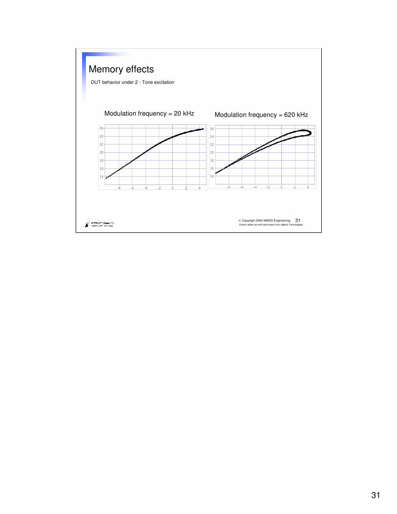
Memory effects !
31
31Certain slides are with permission from Agilent Technologies
Copyright 2004 NMDG Engineering
Memory effectsDUT behavior under 2 - Tone excitation
-8 -6 -4 -2 0 2 4
14
16
18
20
22
24
26
-8 -6 -4 -2 0 2 4
14
16
18
20
22
24
26
Modulation frequency = 20 kHz Modulation frequency = 620 kHz

32
32Certain slides are with permission from Agilent Technologies
Copyright 2004 NMDG Engineering
Applications
Transistor reliability Transistor model verification (ICCAP / ADS) Transistor model tuning System level characterization Scattering functions Memory effect Dynamic bias High Speed Digital PA design using waveform engineering Conclusions

33
33Certain slides are with permission from Agilent Technologies
Copyright 2004 NMDG Engineering
What is “Dynamic Bias Behavior”?
Freq. (GHz)
1 2DCFreq. (GHz)
1DC
Input Voltage Output Current
1V 2I
Dynamic Bias BehaviorFrequency Domain:
Generation of Low Frequency Intermodulation Products
Time Domain:“Beating” of the Bias

34
34Certain slides are with permission from Agilent Technologies
Copyright 2004 NMDG Engineering
Dynamic Bias: Measurement Principle
TUNER
RF Data Acquisition
Dynamic Bias Data Acquisition
CurrentProbe
Bias 1Supply
CurrentProbe
Bias 2SupplyComputer
35
35Certain slides are with permission from Agilent Technologies
Copyright 2004 NMDG Engineering
0 0.2 0.4 0.6 0.8 1 1.2-2
-1.5
-1
-0.5
0
0.5
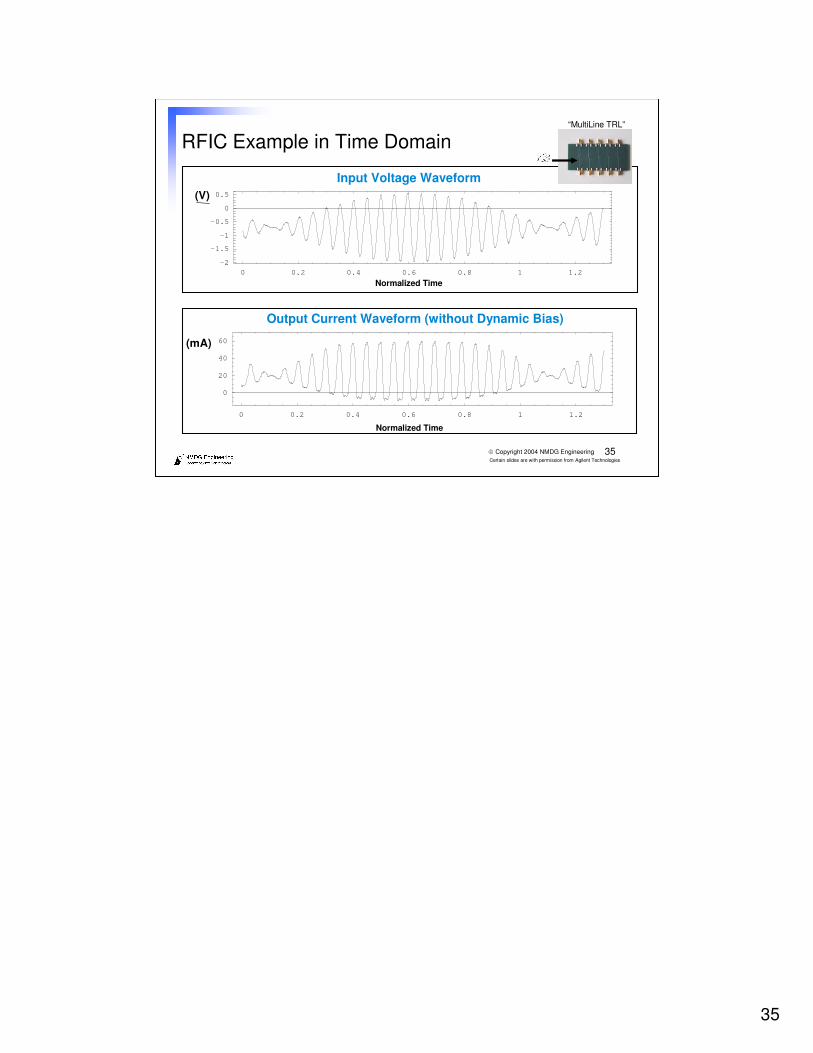
RFIC Example in Time Domain
0 0.2 0.4 0.6 0.8 1 1.2
0
20
40
60
Output Current Waveform (without Dynamic Bias)
(mA)
(V)
Normalized Time
Normalized Time
Input Voltage Waveform
“MultiLine TRL”

36
36Certain slides are with permission from Agilent Technologies
Copyright 2004 NMDG Engineering
0 0.2 0.4 0.6 0.8 1 1.2
0
20
40
60
0 0.2 0.4 0.6 0.8 1 1.2
25
30
35
40
45
Adding Measured Dynamic Bias
Output Current Waveform (including Dynamic Bias)
(mA)
(mA)
Normalized Time
Normalized Time
Dynamic Bias Current Waveform

37
37Certain slides are with permission from Agilent Technologies
Copyright 2004 NMDG Engineering
Applications
Transistor reliability Transistor model verification (ICCAP / ADS) Transistor model tuning System level characterization Scattering functions Memory effect Dynamic bias High Speed Digital PA design using waveform engineering Conclusions

38
38Certain slides are with permission from Agilent Technologies
Copyright 2004 NMDG Engineering
High-Speed Digital Measurements
System rise time 7ps – Compare 12ps for 50GHz
scope
Some Gibbs phenomenon No (random) jitter No slow tail
– cable response corrected
DUT: 40 Gb Data Amp at 1.25 GB/s
39
39Certain slides are with permission from Agilent Technologies
Copyright 2004 NMDG Engineering
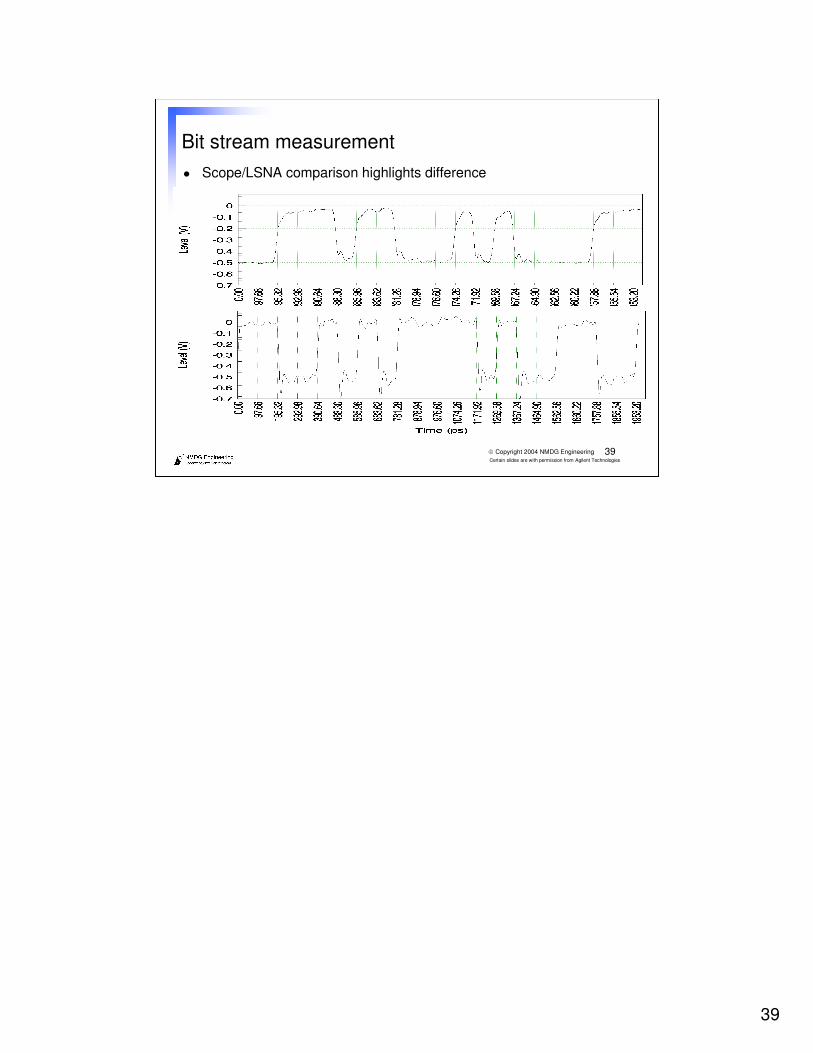
Bit stream measurement Scope/LSNA comparison highlights difference

40
40Certain slides are with permission from Agilent Technologies
Copyright 2004 NMDG Engineering
Eye diagram measurement at 10 GB/s

41
41Certain slides are with permission from Agilent Technologies
Copyright 2004 NMDG Engineering
Applications
Transistor reliability Transistor model verification (ICCAP / ADS) Transistor model tuning System level characterization Scattering functions Memory effect Dynamic bias High Speed Digital PA design using waveform engineering Conclusions

42
42Certain slides are with permission from Agilent Technologies
Copyright 2004 NMDG Engineering
LSNA and ATS tuners (Maury)
LoadTuner
SourceTuner
Broadband Receiver
FixtureTermination
orSecond source
Practical solution based on passive tuners …
LSNA
… to minimize losses
In practice, passive tuners need to be as close as possible to the device under test. This complicates the calibration process, because one needs to take the changing tuner characteristics into account. On top of that, the device under test can be a transistor in a fixture. Therefore one also needs to de-embed the fixture.
43
43Certain slides are with permission from Agilent Technologies
Copyright 2004 NMDG Engineering
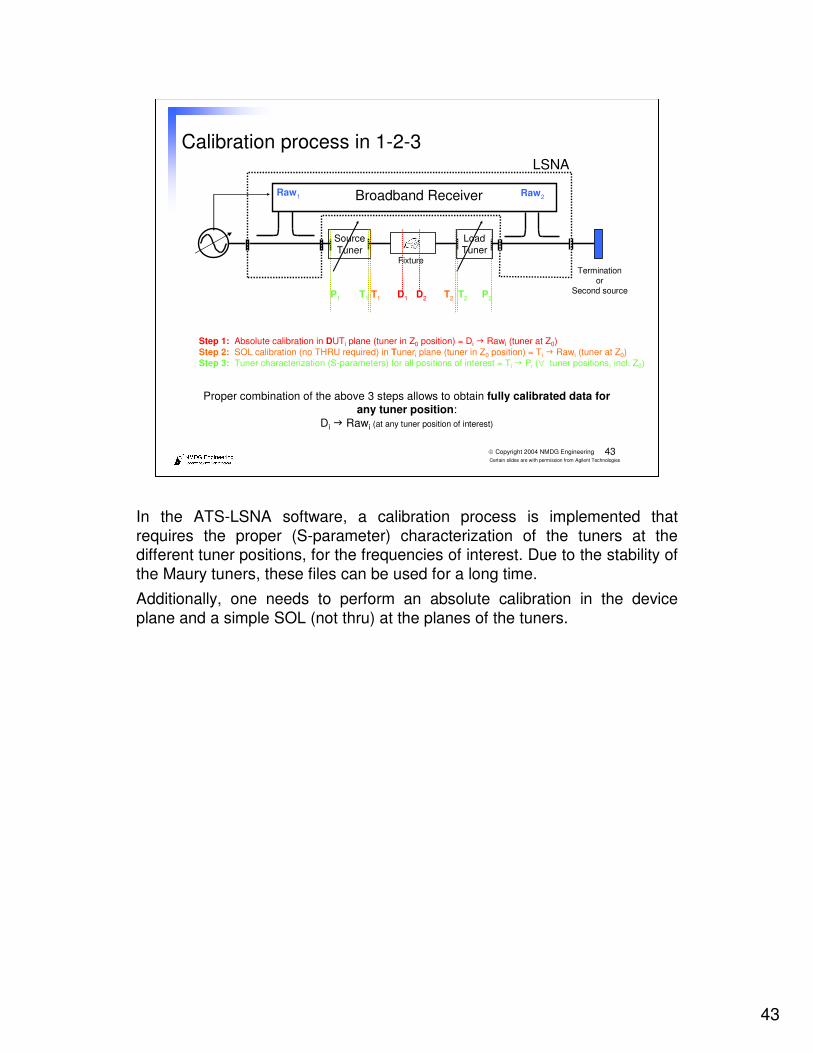
Calibration process in 1-2-3
SourceTuner
Broadband Receiver
FixtureTermination
orSecond source
LoadTuner
LSNA
Step 1: Absolute calibration in DUTi plane (tuner in Z0 position) = Di Rawi (tuner at Z0) Step 2: SOL calibration (no THRU required) in Tuneri plane (tuner in Z0 position) = Ti Rawi (tuner at Z0) Step 3: Tuner characterization (S-parameters) for all positions of interest = Ti Pi (∀ tuner positions, incl. Z0)
D1 D2T1 T2P1 T1 T2 P2
Raw1 Raw2
Proper combination of the above 3 steps allows to obtain fully calibrated data for any tuner position:
Di Rawi (at any tuner position of interest)
In the ATS-LSNA software, a calibration process is implemented that requires the proper (S-parameter) characterization of the tuners at the different tuner positions, for the frequencies of interest. Due to the stability of the Maury tuners, these files can be used for a long time.
Additionally, one needs to perform an absolute calibration in the device plane and a simple SOL (not thru) at the planes of the tuners.

44
44Certain slides are with permission from Agilent Technologies
Copyright 2004 NMDG Engineering
ATS - LSNA Use: Calibration SupportSOLTLRRM
Here the ATS interface is shown in combination with some dialog boxes used during the calibration of the LSNA.
Presently SOLT and LRRM are supported. Multiline TRL can be provided under consulting. The advantage of using multiline TRL, is to be able to calibrate up to the level of a packaged RFIC.
45
45Certain slides are with permission from Agilent Technologies
Copyright 2004 NMDG Engineering
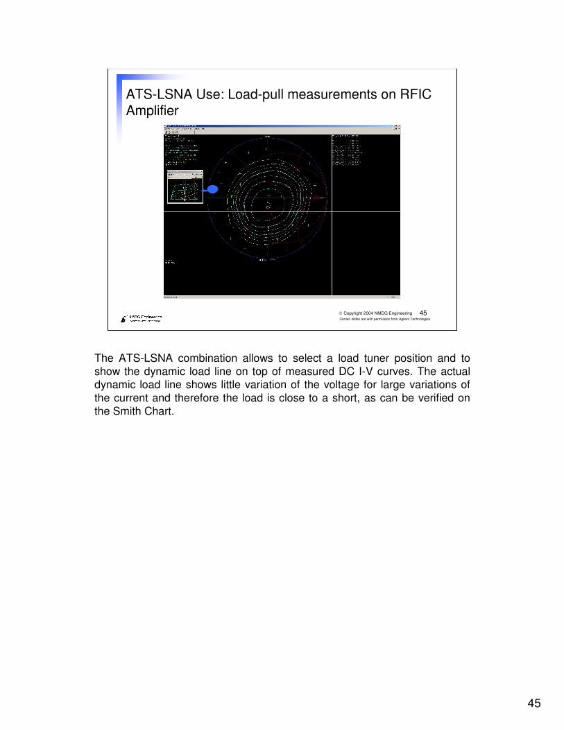
ATS-LSNA Use: Load-pull measurements on RFIC Amplifier
The ATS-LSNA combination allows to select a load tuner position and to show the dynamic load line on top of measured DC I-V curves. The actual dynamic load line shows little variation of the voltage for large variations of the current and therefore the load is close to a short, as can be verified on the Smith Chart.

46
46Certain slides are with permission from Agilent Technologies
Copyright 2004 NMDG Engineering
ATS-LSNA Use: Measurement Representations
The accurate voltages and currents or incident and reflected waves, measured and calibrated up to the DUT plane, can be visualized in different ways.
47
47Certain slides are with permission from Agilent Technologies
Copyright 2004 NMDG Engineering
Conclusions
LSNA opens complete new horizons to improve the design and testing process in different ways when nonlinear behavior is involved
Contact– Marc Vanden Bossche– [email protected]– www.nmdg.be


![Index [users.skynet.be]users.skynet.be/fa328237/publiek/PDF/Index_THEOSOFIE_Vol... · 2013. 3. 22. · Theosofie, Vrijheid van Gedachte en Dogmatisme - dl.1 15 Janus: De God van het](https://img.pdfslide.net/doc/110x75/60e9d05435489a2f3e564a8d/index-users-users-2013-3-22-theosofie-vrijheid-van-gedachte-en-dogmatisme.jpg)