Embed Size (px)
Citation preview

1 / 12
Large transverse thermoelectric figure of merit in a Dirac semimetal 1,2Junsen Xiang, 1,3Sile Hu, 1,3Meng Lyu, 1,3Wenliang Zhu, 1,3Chaoyang Ma, 2Ziyu Chen, 1,4Frank
Steglich, 1,3,5Genfu Chen, and 1,3,5Peijie Sun
1BeijingNationalLaboratoryforCondensedMatterPhysics,InstituteofPhysics,ChineseAcademyofSciences,Beijing100190,China2DepartmentofPhysics,KeyLaboratoryofMicro‐NanoMeasurement‐ManipulationandPhysics,BeihangUniversity,Beijing100191,China3UniversityofChineseAcademyofSciences,Beijing100049,China4MaxPlanckInstituteforChemicalPhysicsofSolids,01187Dresden,Germany5SongshanLakeMaterialsLaboratory,Dongguan,Guangdong523808,China
Thermoelectric (TE) conversion in conducting materials is of eminent importance for
providing renewable energy and solid-state cooling. Although traditionally, the Seebeck
effect plays a key role for the TE figure of merit zST, it encounters fundamental constraints
hindering its conversion efficiency. Most notably, there are the charge compensation of
electrons and holes that diminishes this effect, and the intertwinement of the corresponding
electrical and thermal conductivities through the Wiedemann-Franz (WF) law which makes
their independent optimization in zST impossible [1, 2]. Here, we demonstrate that in the
Dirac semimetal Cd3As2 the Nernst effect, i.e., the transverse counterpart of the Seebeck
effect, can generate a large TE figure of merit zNT. At room temperature, zNT ≈ 0.5 in a small
field of 2 T; it significantly surmounts its longitudinal counterpart zST for any field and
further increases upon warming. A large Nernst effect is generically expected in topological
semimetals, benefiting from both the bipolar transport of compensated electrons and holes
and their high mobilities. In this case, heat and charge transport are orthogonal, i.e., not
intertwined by the WF law anymore. More importantly, further optimization of zNT by tuning
the Fermi level to the Dirac node can be anticipated due to not only the enhanced bipolar
transport, but also the anomalous Nernst effect arising from a pronounced Berry curvature
[3 – 6]. A combination of the former topologically trivial and the latter nontrivial advantages
promises to open a new avenue towards high-efficient transverse thermoelectricity.
Thermoelectric (TE) devices can convert heat into electrical energy but may also be used as a heat
pump in which electricity can drive a Peltier cooler. Various materials and differing concepts have
been employed in order to achieve practical application [1, 2]. Here, the dimensionless figure of
merit, zST = TSxx2/ρxxxx, plays the key role in characterizing the TE conversion efficiency. It contains
the absolute temperature T, the Seebeck coefficient Sxx, the electrical resistivity ρxx and the thermal
conductivity xx. The subscript ‘xx’, which denotes diagonal components of the corresponding transport matrix, is intentionally added to distinguish from the off-diagonal counterparts that will
define the transverse counterpart zNT. In classical TE materials, optimization of zST meets severe
limitations. Most important is charge compensation of electrons and holes that contribute oppositely
to Sxx (Fig. 1a). Also, the Lorenz number fundamentally ties ρxx and the electronic contribution to

2 / 12
thermal conductivity xxe, i.e., L = xx
eρxx/T. L coincides with Sommerfeld’s constant L0 = 2.44 × 10⁻⁸
WꞏΩꞏK2 for dominating elastic scatterings (the Wiedemann-Franz, WF, law). Though the WF law is
frequently violated to some extent at finite temperatures, it makes independent optimization of ρxx and
xx for high zST impossible. Any new designing principle circumventing (some of) these limitations will potentially achieve a big advance in TE application, such as the electron crystal-phonon glass
approach, which proposes to minimize xx while simultaneously keeping ρxx low by crystal-structure engineering [7].
A number of suited TE materials have recently been revisited and turned out to be topological
materials [2, 8]. Except for some basic properties connecting both types of materials [8], e.g., the
presence of heavy elements and small band gaps, characteristic reasons for advanced TE transport
in topological materials have also been discussed. These include the specific band complexities [9 -
11] and charge relaxation processes [4,12,13] generally related to topological materials. However,
the aforementioned topologically trivial limitations for TE performance exist for topological materials
as well. Another, largely unexplored, prominent feature of these materials is the strong
magnetic-field response, pertinent particularly to topological semimetals [14,15]: Here, in addition to
the well-known chiral anomaly in the magneto-electrical conductivity, a strong effect of magnetic
fields on the Seebeck effect was recently realized, too. For example, Wang et al. have reported a
largely enhanced zST from 0.2 to 1.2 by applying a field B = 7 T at T = 370 K for the Dirac semimetal
Cd3As2 [16]. Moreover, a large, nonsaturating Seebeck effect in quantizing magnetic fields has
been theoretically predicted for Dirac/Weyl semimetals [17].
In case a magnetic field Bz is applied orthogonally to the temperature gradient dTx, a transverse
counterpart (Sxy) of Sxx, known as the Nernst effect (Fig. 1b), appears too. Traditionally, Sxy has
been intensively investigated mainly in elemental Bi and several of its binary alloys, like Bi-Sb [18 –
21], where its potential for TE application was first proposed. The key ingredients for significant
values of Sxy(Bz) revealed in these works include: A large product of ωcτ (ωc is the cyclotron
frequency and τ the relaxation time) and a small Fermi energy εF (see SM for explanation why Sxy
tracks ωcτ/ϵF in a single-band approximation), as well as a strong electron-hole compensation that
gives rise to a significant bipolar effect, see Fig. 1b. Interestingly, similar conditions are inherent to a
large number of recently discovered topological semimetals [15]. Indeed, a large Nernst power
factor, Sxy2/ρ, was found in NbP [22] where, however, a large thermal conductivity prevents
realization of a sizable transverse figure of merit zNT. Furthermore, an anomalous Nernst effect
(ANE) due to a pronounced Berry curvature of the related electronic bands, in additional to the
aforementioned topological trivial origins, has been proposed [3 – 6, 23 - 25] for topological
conducting materials with Dirac/Weyl nodes sufficiently close to ϵF. Experimental verifications of this
were reported very recently for NbP [25,26], TaP/TaAs [23] and Cd3As2 [24].
In this paper, we demonstrate that Cd3As2 exhibits a sizable transverse figure of merit which
surmounts its longitudinal counterpart in a wide temperature range above 100 K, amounting to zNT
0.5 (0.7) at T= 300 (350) K in Bz = 2 (2.5) T. These zNT values, after being normalized by the corresponding field, are more than 2 times its longitudinal counter zST in this temperature window.
More importantly, due to the remove of the two constraints that apply inherently to Sxx (see Fig. 1b),
as well as the theoretically predicted addition of the ANE, the transverse thermoelectricity in
3 / 12
topological semimetals appears to be much easier for further optimization by e.g., tuning the Fermi
level.
As shown in Fig. 1c, for Cd3As2 the magnitude of Sxy(T) surpasses that of Sxx(T) already in weak
magnetic fields, e.g. Bz = 1 T, at T > 100 K. This is even clearly demonstrated in Fig. 1d where the
ratio Sxy/Sxx(T) for Bz = 0.5, 1, 2 and 3 T is shown. Furthermore, the initial Nernst coefficient, defined
as Nini = dSxy /dBz at Bz → 0, strongly increases with T and reaches 100 µV/KT at T ≈ 250 K (Fig. 1e)
before decreasing smoothly. Such Nini(T) profile has been interpreted for topological semimetal NbP
[26] as reflecting the T-dependent competition between electron- and hole- bands, i.e., the bipolar
effect. Subsequently, the existence of an enhanced ANE was also emphasized [25], originating
from the shift of the Fermi level ϵF toward the Weyl node with increasing temperature [26]. A larger
transverse relative to longitudinal TE response can also be inferred from the so-called
thermoelectric mobility µT = Nini/Sxx that is as large as its electrical counterpart, the Hall mobility µH;
the latter surmounts 10 m2 V−1s−1 at T = 10 K, see Fig. 1f. A large value of μH pushes the strong field
limit (μHB > 1) down to below 1 T, where ωcτ > 1 is already realized. These properties, in
combination with the extremely low thermal conductivity of Cd3As2 [27, 28], are mainly responsible
for the unprecedented magnitude of transverse thermoelectricity of this compound in low fields.
Figure 2 compiles the full set of magneto-transport coefficients for sample S1 (εF = 253 meV, see
SM) at selected temperatures in panels a – e. In panel f, we compare the Nernst effect of this
sample to the previously reported values in ref. 24. See supplementary Fig. S3 for similar results of
sample S4 with a higher εF = 273 meV. Significantly, both Sxx(Bz) and Sxy(Bz) (Fig. 2a and 2b) are
sensitive to small fields. At T > 50 K, they are substantially enhanced up to a certain value of Bz 3
T, then the former quantity tends to saturate and the latter assumes a maximum, see Fig. 2c, where
Sxx(Bz) is compared to Sxy(Bz) for T = 250 K. There, the value of Sxy(Bz) can surpass Sxx(Bz) at fields
as low as Bz 0.6 T and by 50% at 2 T, as already indicated in the ratio Sxy/Sxx(Bz) shown in Fig. 1d. While Sxy(Bz) is substantially larger than Sxx(Bz) in moderate fields, we note that the field
enhancement to the latter is already sizable and has been reported to cause a marked increase of
zST in Cd3As2 [16], as mentioned in the introduction.
As far as TE conversion is concerned, the increase of ρxx(Bz) (Fig. 2d) is almost compensated by
the corresponding decrease of κxx(Bz) (Fig. 2e), both of which appear in the denominator of zST. In
other words, given that the WF law roughly holds at T 100 K, the thermal conductivity measured in this temperature range is predominantly electronic in origin and κxxρxx ≈ κxx
eρxx = L0T. Indeed, as
demonstrated in Fig. 2e for T =150 K, the significant decrease of κxx(Bz) up to Bz ≈ 2 T can be
explained by the estimated κxxe(Bz) based on the WF law (dashed line). On the other hand, the
phonon contribution to thermal conductivity, κxxph(T), is negligibly small at T > 100 K compared to
κxxe(T), see Fig. S5. This is due to the intrinsically formed crystallographic vacancies in Cd3As2,
which is Cd-deficient of the ideal Cd4As2 antifluorite formula [27, 28]. Superior electronic transport
properties coexisting with negligible phonon thermal conductivity was also observed in other
topological semimetals such as WP2 [29] and ZrTe5 [30]. This situation yields an ideal playground
for TE manipulation: Here, zST Sxx2/L0 and Sxx is the only free parameter; a value of Sxx ≥ 155 µV/K
would lead to zST ≥ 1. The same argument applies to the Nernst effect as well.

4 / 12
To interpret the large Nernst effect in Cd3As2, comparison with other semimetals is instructive.
Qualitatively similar profiles of both Sxx(Bz) and Sxy(Bz) as observed in Cd3As2 have been observed
in topological semimetal Pb1−xSnxSe with x = 0.23, too [31]. There, low-field values of Sxy(Bz) are
somewhat lower but still sizable. For example, Sxy(Bz = 2 T) ≈ 50 µV/K at T = 250 K. These values
are, however, much smaller than the corresponding values of Sxx(Bz). The situation that Sxx(T, Bz) ≫
Sxy(T,Bz) in a large parameter space indicates a much reduced bipolar transport in the latter
compound, qualifying it as a state-of-the-art (longitudinal) TE material [1, 2, 31]. Consequently,
rapid increase of both Sxx(Bz) and Sxy(Bz) in Pb1−xSnxSe (x = 0.23) in low fields and at low
temperatures (T < 150 K) has been successfully approached by a single, high-mobility band [31]. It
imposes a competition between longitudinal and transverse differential logarithmic conductivities D
= ∂lnσxx/∂ε and DH = ∂lnσxy/∂ε at the Fermi level εF. It is this competition that determines the
characteristic profiles of Sxx(Bz) and Sxy(Bz). By employing the experimentally obtained conductivity
matrix elements σxx(Bz) and σxy(Bz), one can fit the measured Sxx(Bz) and Sxy(Bz) of Cd3As2
independently. However, the obtained values of DH−D from the two fittings are already different at T
= 50 K and the discrepancy further increases with T up to room temperature, see supplementary Fig.
S6. Similar behavior has been discussed as originating from the increasing electron-hole bipolar
effect beyond the one-band hypothesis [31]. This inference applies to Cd3As2 as well, and is in
consistent to the inference made from the Nini(T) profile (Fig. 1e), which reveals a maximum near
room temperature. Further evidence of bipolar transport in Cd3As2 comes from the non-linear ρxy(Bz)
behaviors that indicate a dominating electron band and a hole band that increasingly compensates
upon warming, see supplementary Figs. S7.
In analogy to zST that is defined from Sxx, its transverse counterpart can be defined from Sxy [19],
𝑧 𝑇 𝑇
. (1)
Here, κxx and ρyy take the values measured along x and y directions, respectively. This definition
can be easily rationalized for Nernst configuration, where the induced electrical current (|| y) is
orthogonal to the driving thermal current (|| x), see Figs. 1b, 3a, and ref. 19. In all our samples of
Cd3As2, ρ is actually rather isotropic at least within the (112) plane that we focus on in this work, see
supplementary Fig. S4. We therefore use the simultaneously measured ρxx (rather than the
separately measured ρyy) to compute zNT in order to reduce systematic errors. As shown in Fig. 3b,
the superiority of the transverse over the longitudinal TE effect in Cd3As2 is immediately apparent:
zNT(Bz) exhibits a maximum which, at T > 150 K, is not only higher but also occurs at a lower field
compared to the maximum in zST(Bz). These maximum values, denoted as zNTmax and zSTmax,
respectively, are shown as a function of T in Fig. 3c. There, zNTmax is increasingly enhanced with
temperature over its longitudinal counterpart by, e.g., approximately 50% at T = 350 K. After being
normalized by their corresponding fields as zNTmax/Bzmax, the contrast between the two
configurations becomes even more striking, see Fig. 3d. Above T = 150 K, the maximum zT value
per Tesla of the transverse TE configuration exceeds its longitudinal counterpart by about a factor
of two in a wide temperature range.
Despite its marked increase at low fields, the value of zNT is still inadequate for practical
applications. A key parameter yet to be optimized is the Fermi energy εF, which determines the
magnitude of not only the one-band and bipolar diffusion contributions to Sxy [21, 32], but also the

5 / 12
ANE [23 - 26]. A reduction of εF is expected to enhance all these contributions in a Dirac semimetal.
To clarify this point, we have derived the values of εF for all the employed samples from the
experimentally observed quantum oscillations in ρxx(Bz), see Fig. S8. Note that, within the
charge-neutrality condition, εF is measured with respect to the energy of minimal electronic density
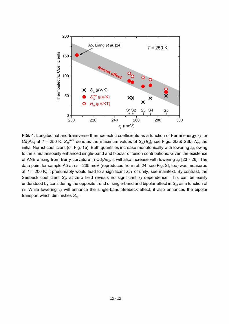
of states, i.e., the energy of the Dirac node. As shown in Fig. 4, εF spans the range of roughly 250 −
290 meV from sample S1 to S5. Most importantly and instructively, both Sxymax and Nini, which
characterize the magnitude of the Nernst effect, increase monotonically with lowering εF, see Fig. 4.
A simple extrapolation indicates that Sxymax would be greater than 155 µV/K if εF < 200 meV.
Unfortunately, our sample syntheses could not yield reliable samples with εF < 250 meV. One batch
(A5) reported in ref. [24], with Sxymax ≈ 150 µV/K at Bz = 5 T, is reproduced in Fig. 2f; the Fermi
energy of this sample is estimated to be εF ≈ 205 meV (see SM), which indeed meets our
expectation for larger Sxy, cf. Fig. 4. Given the dominating κxxe in this temperature range, this very
sample should exhibit a maximum zNT of order unity at T = 200 K. This simple relation between the
Nernst effect and εF reflects the aforementioned monotonic enhancement of all quantities
contributing to Sxy upon decreasing εF. By contrast, for the five samples investigated we could not
find any significant variation of the zero-field values of Sxx. As discussed in the introduction, this is
most likely due to a competition between bipolar and single-band Seebeck effects, where the former
diminishes and the latter enhances the value of Sxx upon lowering εF [20].
Our observations of large Sxy(T, Bz) values exceeding those of Sxx(T, Bz) in a wide parameter space
is not specific to Cd3As2, but is generally expected in topological semimetals. An extraordinarily
large value of Sxy (T = 109 K; Bz = 9 T) ≈ 800 µV/K was recently observed in NbP, and found to be
two orders of magnitude larger than the corresponding Sxx value [26]. This is not surprising because
in NbP εF = 8.2 meV is very close to the Weyl node, leading to symmetric electron and hole
excitations that produce a particularly strong bipolar contribution to Sxy, as well as an enhanced
Berry curvature strength [23, 25] that gives rise to very large value of ANE. Unfortunately, the
thermal conductivity of NbP (κ 250 W/Km at T = 300 K) is much too large to obtain a sizable zNT value [22, 33]. In WP2, too, a large Nernst was observed, e.g., Sxy (T = 3.66 K, Bz = 5 T) ≈ 1 mV/K,
although at much lower temperatures [34]. As has been discussed, due to the generically high
mobility of all the pertinent Dirac/Weyl semimetals, the strong-field limit with ωcτ > 1 can be easily
accessed by a field as low as 1 T. There, a larger Sxy over Sxx is anticipated, resembling the case of
dominating transverse electrical conductivity with σxy > σxx, see Fig. 1d and refs. 26 & 34. This is a
field accessible even by commercial permanent magnet like Nd2Fe14B. Recently, Nernst effect in
the absence of external field has been observed in a magnetic topological semimetal [35]. This
certainly deserves more attention in future.
As already demonstrated for Cd3As2 [24], a steplike increase of Sxy(Bz) at low field arising from
enhanced Berry curvature and characterizing the ANE is a significant additive to the conventional
(diffusive) Nernst effect. This occurs if the Fermi level is sufficiently reduced towards the Dirac node
[6, 23, 25], which may be achieved by a well-controlled sample synthesis. This situation appears to
be realized for the case of sample A5 in ref. 24, for which the maximum value of Sxy(Bz) is
reproduced in Fig. 4. A direct identification of a steplike ANE for our samples seems unlikely, see
Figs. 2b and S3b. However, such a contribution is presumably involved in our samples, too, though
being expected to be smaller given their higher ϵF. Whether in future one can experimentally sort out

6 / 12
the evolution of ANE with ϵF appears to be instructive for improvement of Sxy. The largely
unexplored ANE in this compound, together with the enhanced diffusive contribution of bipolar
transport, promises a large room for further optimization of zNT. This is believed to be achievable
simply by tuning the Fermi energy (Fig. 4). Apart from their fundamental advantages discussed
above, transverse TE devices also have remarkable merits due to their unique configuration
geometry. i) The TE conversion output of such devices scales with the sample size along y relative
to x, which allows for various possibilities of shape engineering in order to maximize conversion
efficiency [19]; ii) Both electrons and holes of a single material are already involved in the Nernst
effect, leaving out the traditional idea of employing both n and p-type materials in one TE device,
see Fig.3a; iii) Separation of electrical and heat flows into two orthogonal directions removes the
fundamental constraint of the WF law; utilization of anisotropic transport becomes possible through,
e.g., combining low κxx and low ρyy in one material.
METHODS
Sample synthesis. Single crystals of Cd3As2 were grown by self-transport technique. Stoichiometric
amounts of cadmium and arsenic were first sealed in an evacuated quartz ampoule. The quartz
ampoule was heated to 850 and then quenched in liquid nitrogen. The obtained polycrystalline
Cd3As2 was filled in a quartz ampoule again. After evacuating and sealing, the ampoule was placed
in a two-zone furnace with a temperature gradient from 575 to 500 for 10 days, and then naturally
cooled down to room temperature. The single crystals grow in bulk form with well-defined facets,
see inset of Fig. S1. X-ray diffraction of powered and single-crystalline samples was performed to
confirm the proper crystal structure and the orientation (Fig. S1). The residual resistivity ratio RRR =
ρxx(300K)/ρxx(2K) is between 5 and 10 for all the samples investigated. This is in agreement with
most published works on this compound [16, 27], except for several batches reported in ref. [36].
Transport measurements. The three relevant thermal transport coefficients Sxx, Sxy and κxx, as well
as resistivity ρxx were measured simultaneously and adiabatically in a magnetic field Bz applied
orthogonal to temperature gradient dTx (Figs. 1a, 1b and 1c inset). dTxx was monitored by a
field-calibrated, thin Chromel-AuFe0.07% thermocouple (φ = 25 µm), cf. Fig. S2. All the five
samples investigated in this work were bar-shaped by polishing the as-grown samples to typical
dimension (3−4) × (1−2) × (0.3−0.5) mm3, see Fig. 1c inset. Note that the field-induced Nernst
voltage Ey is geometry (more precisely, the length-to-width ratio) dependent. By convention, we
adopt the geometry-normalized Nernst effect Sxy = A Ey/dTx, with A = Lx/Ly being the length ratio of
thermal and electrical flow [20]. All the thermal-transport measurements were performed within the
(112) plane, with magnetic field Bz applied normal to it. The five samples discussed in this work
have slightly different Fermi energies, which were estimated from the respective quantum
oscillations in resistivity (Figs. 4 and S8).
References
1. Snyder, G. J. and Toberer, E. S. Complex thermoelectric materials. Nat. Mater. 7, 105-114
(2006).
2. He, J. and Tritt, T. M. Advances in thermoelectric materials research: Looking back and moving
7 / 12
forward. Science 357, 1369 (2017).
3. Xiao, D., Yao, Y., Fang, Z. and Niu, Q. Berry-phase effect in anomalous thermoelectric transport,
Phys. Rev. Lett. 97, 026603 (2006).
4. Lundgren, R., Laurell, P. and Fiete, G. A. Thermoelectric properties of Weyl and Dirac semimetals,
Phys. Rev. B 90, 165115 (2014).
5. Sharma, G . , Goswami, P. and Tewari, S. Nernst and magnetothermal conductivity in a lattice
model of Weyl fermions, Phys. Rev. B 93, 035116 (2016).
6. Noky, J., Gooth, J., Felser, C. and Sun, Y. Characterization of topological band structure away from
the Fermi level by the anomalous Nernst effect. Phys. Rev. B 98, 241106 (R) (2018).
7. Slack, G. A. in CRC Handbook of Thermoelectrics (ed Rowe D. M.) Ch. 9 (CRC Press, 1995).
8. Muchler, L., Casper, F., Yan, B.H., Chadov, S., Felser, C. Topological Insulators and thermoelectric
materials, Phys. Status Solidi RRL 7, 91 (2013).
9. Pal, K., Anand, S., and Waghmare, V. Thermoelectric materials of materials with nontrivial electronic
topology, J. Mater. Chem. C 3, 12130 (2015).
10. Shi, H., David, P., Du, M-H. and Singh, D.J. Connecting thermoelectric performance and
topological-insulator behavior: Bi2Te3 and Bi2Te2Se from first principles, Phys. Rev. Appl. 3, 014004
(2015).
11. Devender, Gehring, P., Gaul, A., Hoyer, A., Vaklinova, K., Mehta, R.J., Burghard, M., Borca-Tasciuc,
T., Singh, D. J., Kern, K. and Ramanath, G. Harnessing Topological Band Effects in Bismuth
Telluride Selenide for Large Enhancements in Thermoelectric Properties through Isovalent Doping,
Adv. Mater. 28, 6436 (2016).
12. Xu, Y., Gan, Z., and Zhang, S-C. Enhanced thermoelectric performance and anomalous Seebeck
effect in topological insulators, Phys. Rev. Lett. 112, 226801 (2014).
13. Takahashi, R. and Marukami, S. Thermoelectric transport in topological insulators. Semicond. Sci.
Technol. 27, 124005 (2012).
14. Wang, S., Lin, B.C., Wang, A.Q., Yu, D.P. and Liao, Z.M. Quantum transport in Dirac and Weyl
semimetals: a review. Advances in Physics X 2, 518 (2017).
15. Armitage, N. P., Mele, E. J., Vishwanath, A. Weyl and Dirac Semimetals in Three-Dimensional
Solids. Rev. Mod. Phys. 90, 015001 (2018).
16. Wang, H. et al., Magnetic-field enhanced high-thermoelectric performance in topological Dirac
semimetal Cd3As2 crystal, Sci. Bull. 63, 411 (2018).
17. Skinner, B. and Fu, L. Large, nonsaturating thermopower in a quantizing magnetic field, Sci. Adv. 4,
eaat2621 (2018).
18. Yim, W. M. and Amith, A. Bi-Sb alloys for magneto-thermoelectric and thermomagnetic cooling. Solid
State Electronics 15, 1141 (1972).
19. Goldsmid, H. J. The Ettingshausen figure of merit of bismuth and bismuth-antimony aloys. Brit. J.
Appl. Phys. 14, 271 (1963).
20. Goldsmid, H. J. Introduction to thermoelectricity (Springer Series in Materials Science). (Springer,
2009).
21. Behnia, K. Measson, M-A. and Kopelevich, Y. Nernst effect in semimetals: The effective mass and
the Figure of merit. Phys. Rev. Lett. 98, 076603 (2007).
22. Fu, C. et al., Large Nernst power factor over a broad temperature range in polycrystsalline Weyl
semimetal NbP, Energy & Environ. Sci. 11, 2813 (2018).
23. Caglieris, F., Wuttke, C., Sykora, S., Suss, V., Shekhar, C., Felser, C., Buchner, B. and Hess, C.

8 / 12
Anomalous Nernst effect and field-induced Lifshitz transition in the Weyl semimetal TaP and TaAs.
Phys. Rev. B 98, 201107(R) (2018).
24. Liang, T., Lin, J., Gibson, Q., Gao, T., Hirschberger, M., Liu, M., Cava, R.J. and Ong, N.P.
Anomalous Nernst effect in the Dirac semimetal Cd3As2. Phys. Rev. Lett. 118, 136601 (2017).
25. Sharma, J., Moore, C., Saha, S. and Tewari, S. Nernst effect in Dirac and inversion-asymmetric Weyl
semimetals. Phys. Rev. B 96, 195119 (2017).
26. S. J. Watzman, T.M. McCormick, C. Shekhar, S-C. Wu, Y. Sun, A. Prakash, C. Felser, N. Trivedi and
J.p. Heremans, Dirac dispersion generate unusually large Nernst effect in Weyl semimetals, Phys.
Rev. B 97, 161404 (R) (2018).
27. Zhang, C., Zhou, T. et al., Unexpected low thermal conductivity and large power factor in Dirac
semimetal Cd3As2. Chin. Phys. B 25, 017202 (2016).
28. Ali, M.N., Gibson, Q., Jeon, S., Zhou, B.B., Yazdani, A. and Cava, R. J. The crystal and electronic
structures of Cd3As2, the three-dimensional electronic analogue of graphene. Inorg. Chem. 53,
4062-4067 (2014).
29. Gooth, J., Mneges, F., Kumar, N., Suβ, V., Shekha, C., Sun, Y., Drechsle, U., Zierold, R., Felser,
C., and Gotsmann, B. Thermal and electrical signatures of a hydrodynamic electron fluid in
tungsten diphosphide. Nat. Commun. 9, 4093 (2018).
30. Zhu, J. et al., Record-low and anisotropic thermal conductivity of a quasi-one-dimensional bulk
ZrTe5 single crystal. ACS Appl. Mater. Interfaces 47, 40740 (2018).
31. Liang,T., Gibson, Q., Xiong, J., Hirschberger, M., Koduvayur, S.P., Cava, R.J. and Ong, N.P.
Evidence for massive bulk Dirac fermions in Pd1-xSnxSe from Nernst and thermopower experiments.
Nature Communi. 4, 2696 (2013).
32. Behnia, K. and Aubin, H. Nernst effects in metals and superconductors: A review of concepts and
experiments. Rep. Prog. Phys. 79, 046502 (2016).
33. Stockert, U. et al., Thermopower and thermal conductivity in the Weyl semimetal NbP. J. Phys.:
Condens. Matter 29, 325701 (2017).
34. Zhu, Z. et al., Quantum oscillations, thermoelectric coefficients, and the Fermi surface of
semimetallic WTe2. Phys. Rev. Lett. 114, 176601 (2015).
35. Guin, S.N. et al., Zero-field Nernst effect in a ferromagnetic Kagome-lattice Weyl-semimetal
Co3Sn2S2. Adv. Mater. 31, 1806622 (2019)
36. Liang, T., Gibson, Q., Ali. M. N., Liu, M., Cava, R. J. and Ong, N. P., Ultrahigh mobility and giant
magnetoresistance in the Dirac semimetal Cd3As2. Nat. Mater. 14, 280 (2015).
Figures
9 / 12
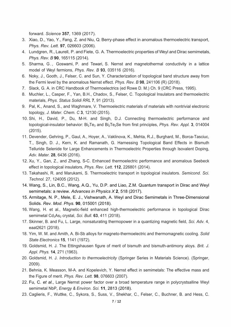
FIG. 1: Comparison of longitudinal and transverse thermoelectric effects in Cd3As2. (a, b)
Schematic illustrations of the Seebeck (Sxx) and the Nernst (Sxy) effects for a compensated
conductor. They measure the longitudinal and transverse thermoelectric voltages Ex and Ey,
respectively, over a temperature difference dTx. For the latter effect, an orthogonal field Bz is
needed. Note the diminished Sxx in (a), as compared to the enhanced Sxy in (b) due to electron-hole
bipolar conduction. As heat (|| x) and electric flux (|| y) are orthogonal in the latter, constraints of the
WF law is circumvented when considering thermoelectric application. (c) Sxy(T) measured at Bz = 1
T, as compared to Sxx(T) of Cd3As2. From the quasi-linear behavior of Sxx(T), a rough estimate of
the Fermi energy εF = 305 meV can be obtained by assuming Sxx(T) = 2/2 kB/e kBT/εF for simple
metals. Inset: The photo image of the sample S1 mounted on sample holder. (d) The transverse to
longitudinal thermoelectric ratio Sxy/Sxx at varying field Bz = 0.5, 1, 2 and 3 T is shown as a function
of T. (e) Initial Nernst coefficient Nini(T) defined as Sxy/Bz (Bz → 0). (f) Thermoelectric mobility µT (=
Nini/Sxx) is compared to its electronic analog, i.e., the Hall mobility µH (= RH/ρxx). Their values are
much larger than 1 m2/Vs (i.e., ωcτ > 1 at Bz = 1 T) below room temperature, indicating that both
electric and thermoelectric responses in small fields are predominantly transverse. Data shown in
panels c-f were measured for sample S1, with x || [110] and z (112) plane.
0 100 200 300 4000
50
100
150
N ini
(V
/KT
)
T (K)
0 50 100 150 200 250 300 3500.0
0.5
1.0
1.5
2.0
Sxy
/Sxx
T (K)
0.5 T 1 2 3
10 1000
5
10
15
H
(m
2 /Vs)
T (K)
T
0 50 100 150 200 250 300 350
0
20
40
60
80
100
|Sxx
| (0T)
|Sxy
| (1T)
|Sxx
|, |S
xy| (V
/K)
T (K)
f
edc
b
a

10 / 12
FIG. 2: Electrical and thermal transport coefficients recorded in a perpendicular field scan at varying
temperatures for sample S1. The Seebeck coefficient Sxx(Bz) and Nernst effect Sxy(Bz) are shown in
(a) and (b), respectively. In (c), Sxx(Bz) and Sxy(Bz) for T = 250 K are compared, with the latter
largely exceeding the former between Bz = 1 and 4 T. (d) and (e) show electrical resistivity ρxx(Bz)
and thermal conductivity κxx(Bz) at the corresponding temperatures, respectively. Because the
electronic contribution κxxe(T) dominates κxx(T) at T > 50 K (see supplementary Fig. S5), the field
enhancement of ρxx(Bz) and the field reduction of κxx(Bz) are nearly compensated when considering
TE application. Namely, κxxρxx L0T in this temperature window. Indeed, as shown in panel (e), the measured κxx(Bz) for T = 150 K can be well appraoched by the calculated κxx
e (= L0T/ρxx) at B < 2 T.
This means that the denominator of the zST expression, ρxxκxx, approximates to a constant and
practically, Sxx and Sxy become the solely free material parameters that determine the TE
performance. (f) Sxy(Bz) measured at T = 200 K for sample S1 is compared to that of A5 reported in
ref. 24. The Fermi energy ϵF is 253 and 205 meV for S1 and A5, respectively, see SM.
0 2 4 6 8 100
40
80
120
Sxx
, Sxy
(V
/K)
Bz (T)
Sxy
(Bz)
- Sxx
(Bz)
c
T = 250 K
-10 -8 -6 -4 -2 0 2 4 6 8 100.0
0.5
1.0
1.5
2.0
2.5
3.0
-10 -8 -6 -4 -2 0 2 4 6 8 101
2
3
4
5
-10 -8 -6 -4 -2 0 2 4 6 8 10-150
-100
-50
0
-10 -8 -6 -4 -2 0 2 4 6 8 10-150
-100
-50
0
50
100
150
xx (
m
cm
)
Bz (T)
50 150 200 250 280 320 350
d e
b
xx (
W/m
K)
Bz (T)
a
e
xx (150 K)
Sxx
(V
/K)
Bz (T)
Sxy
(V
/K)
Bz (T)
0 2 4 6 8 100
50
100
150
200
Sxy
(V
/K)
Bz (T)
S1 (this work) A5 (ref. 24)
T = 200 K
f

11 / 12
FIG. 3: Enhanced transverse thermoelectricity in Cd3As2. (a) Schematics of longitudinal (upper) and
transverse (lower) TE device. While the former needs both p- and n-type materials, the latter uses
only one material with, however, inherent contributions from both types of charge carrier through
biploar transport. (b) zNT(Bz) in comparison to zST(Bz) at selected temperatures for sample S1. (c)
zNTmax and zSTmax, i.e., the maximum values of zNT(Bz) and zST(Bz) observed at certain field Bzmax,
are shown as a function of T. (d) zTmax normalized to the corresponding field Bzmax for both
longitudinal and transverse configurations, where the latter amounts to more than 2 times the
former over a large temperature range above 100 K.
0 2 4 6 8 100.0
0.2
0.4
0.6
0.8
zT
Bz (T)
100 K 150 200 250 350
zNT z
ST
0 50 100 150 200 250 300 3500.0
0.1
0.2
0.3
zST max/B
z
max
zT m
ax /B
zma
x (1/
T)
T (K)
zNT max/B
z
max
0 50 100 150 200 250 300 3500.0
0.2
0.4
0.6
0.8
zNT
max
zST max
zT m
ax
T (K)
a b
c d
12 / 12
FIG. 4: Longitudinal and transverse thermoelectric coefficients as a function of Fermi energy εF for
Cd3As2 at T = 250 K. Sxymax denotes the maximum values of Sxy(Bz), see Figs. 2b & S3b, Nini the
initial Nernst coefficient (cf. Fig. 1e). Both quantities increase monotonically with lowering εF, owing
to the simultansously enhanced single-band and bipolar diffusion contributions. Given the existence
of ANE arising from Berry curvature in Cd3As2, it will also increase with lowering εF [23 - 26]. The
data point for sample A5 at ϵF = 205 meV (reproduced from ref. 24; see Fig. 2f, too) was measured
at T = 200 K; it presumably would lead to a significant zNT of unity, see maintext. By contrast, the
Seebeck coefficient Sxx at zero field reveals no significant εF dependence. This can be easily
understood by considering the opposite trend of single-band and bipolar effect in Sxx as a function of
ϵF. While lowering ϵF will enhance the single-band Seebeck effect, it also enhances the bipolar
transport which diminishes Sxx.
200 220 240 260 280 3000
50
100
150
200
Nernst effect
Sxx
(V/K)
Smax
xy (V/K)
Nini
(V/KT)
S5S4S3S2
Th
erm
oele
ctric
Coe
ffici
ent
s
F (meV)
T = 250 K
S1
A5, Liang et al. [24]