Embed Size (px)
Citation preview

LASER SOURCES
68 LTJ June 2005 No. 2 © 2005 WILEY-VCH Verlag GmbH & Co. KGaA, Weinheim
Laser plasma EUV sources for LithographyDiode pump technology offers new applications
The study of high-temperature plas-mas produced by pulsed laser systems has for a long time been associated with esoteric applications such as laser fusion, x-ray lasers, space propulsion and the like. There are several reasons for this, but one practical reason was simply that the lasers required to produce these plasmas were large, unwieldy and generally single-shot devices (at least minutes between shots). This technology did not lend itself towards applications that were compact, reproducible and potentially automated. However, this is now no longer the case. High-power diode pump technology has transformed the architecture of solid state lasers, reducing by many factors the required thermal dissipation, and there-fore allowing higher repetition rates. Coupled with more compact designs and reduced costs, commercial applications of high-power pulsed lasers, and even laser-produced plasmas are now emerging. Chief among the applications of laser plasmas is now its potential as a light source for what is now called Extreme UV Lithography, or EUVL.
Moore’s Law stipulates that the expectation of the computer chip industry is that the number of transistors on a single computer chip should double every two years ( or even 18 months). This has steadily risen from a few thousand transistors/chip in the early 70’s to over 100 million today. Since the chip itself has stayed almost constant in size, this requires that the density of transistor elements on the chip, continues to increase. This represents the principal challenge for the computer chip designer – how to pro-gressively improve the functionality (i.e., the speed and performance), of the transistor, while at the same time decreasing its size. Remarkably this has occurred over the last 30 years, with Moore’s Law (this being the 40th anniversary of its enunciation ) deman-
MARTIN RICHARDSONMartin Richardson gra-duated from Imperial College, London, in Phy-sics and gained his Ph.D from London University. He is now a Profes-sor of Optics in the School of Optics at the University of Central Florida (Orlando). He directs a research program on the develop-ment of new high power lasers, and their applications to dense laser plasma studies and x-ray generation in the Laser Plasma Laboratory at the Center for Research & Education in Optics & Lasers (CREOL).
THE AUTHOR
●●Martin Richardson
Northrop Grumman Professor of X-ray PhotonicsCollege of Optics & Photonics: CREOL & FPCE University of Central Florida, P.O. Box 162700
Orlando, FL 32816-2700 phone: 001- 407 823-6819
e-mail: [email protected]
WaferCondenser / Illuminator
ReflectiveProjection /Reduction
Optics
EUV Light Source
ReflectiveMask
Resist
Collector Optics
FIGURE 1: Schematic configuration of the principal elements in an EUVL stepper. The EUV source here assumes laser based EUV generation, followed by a condensor/illuminator setup that partially uses gracing incidence optics. The projection (reduc-tion) optics use aspheric mirrors with sub-nm surface error. (Courtesy of intel Corp.)
ding that the minimum (circuit) element size decrease from 10 µm forty years ago to ~ 0.1 µm (or 100 nm) today. Lithography, the basic process by which computer chips are fabricated, is basically a photographic imaging process. Light is projected through a mask, and the resulting two-dimensional light pattern is imaged onto a photo-sensitive polymer and over-coated on a silicon wafer. Subsequent chemical processing of the photo-exposed polymer, or ‘resist’, then produces a three-dimensional relief on the wafer, from which computer circuits can be built. Since the image transmission from mask to wafer is an optical process, the minimum feature size, or the minimum resolvable circuit element, that can be fabricated, is governed by the laws of optics. These state that the minimum resolvable feature that can be fabricated is,
W = k1λ/NA,
where λ is the wavelength of the light used, NA is the numerical aperture of the optics used, and k1,, a factor, ideally > 0.5, that accounts

LASER SOURCES
www.laser-journal.de LTJ 69 © 2005 WILEY-VCH Verlag GmbH & Co. KGaA, Weinheim
In order to maintain the momentum of Moore’s Law, and still use optical lithography, it is obvious that still shorter wavelengths will need to be used. This is where another fundamental limitation raises its head. All materials, particularly all transparent mate-rials in the UV, begin to absorb heavily as the wavelength of light is reduced beyond 190 nm. Therefore, even if there were light sour-ces of sufficient wavelength (and there are some laser light sources), there are no usable refractive optics that can satisfactorily image the mask onto the wafer. The computer in-dustry has been facing this dilemma for the last decade, examining alternative techno-logies (so-called ‘next generation lithogra-phies’) that could remove this log-jam to its further development. Ultimately, within the last few years, this selection process has lead to the emergence of EUVL as the successor to conventional optical lithography, now due to be implemented into chip manufacture from 2009 onwards. In architecture, EUVL is very similar to optical lithography, as it is an imaging system from mask to wafer, except that now the imaging elements are mirrors instead of lenses. These mirrors are covered with special coatings, which allow for high reflectivity in the short UV, or EUV region of the spectrum. Figure 1 shows the general architecture, and the technologies involved. The wavelength of choice, governed by the needs of these mir-
rors is 13.5 nm. Moreover, the spectral ac-ceptance bandwidth of these mirrors is only ~ 2%, or ~ 0.27 nm. This now sets one of the requirements of the light source that will illu-minate these future EUVL steppers. When we examine possible sources of this emission, we quickly realize that plasma sources are the only ones that are suitable and capable of providing the power required. Laser light at this wavelength, either direct laser emission or high harmonic emission, is many orders of magnitude too weak, and synchrotrons have been ruled out for reasons of cost, effi-ciency and complexity. Two plasma sources are currently under development: pulsed discharge sources, and laser plasmas. While the former perhaps can satisfy near-term power needs at lower cost, laser plasmas are considered more likely for the long term. In addition to the wavelength of the emission, both sources must satisfy many other critical requirements. There are tight requirements on spatial and temporal stability, etendue and out-of-band radiation. However, the two most critical parameters are the overall brightness, and the need to preserve the first stage of the EUV optics, which is in line-of-sight with the plasma source. Thus, even small amounts of plasma debris, or high-en-ergy ion emission, is deleterious to the de-licately thin coatings making up the mirror surface. Lithographic stepper manufacturers have traditionally relied on outside suppliers for the radiation sources themselves (such as Cymer Corp and Lambda Physik GmbH for excimer lasers). This will also be the case for EUVL, where now they specify that the required in-band power at the entrance to the stepper (the ‘intermediate focus’) must be > 100W, and the source lifetime must be > 30,000 hrs [1, 2]. Thus the source supplier also assumes responsibility for the collection optics (2 or 3 elements) and their protection from source debris. In principle, the laser-plasma source is con-ducive to these requirements. Long ago, we introduced the concept of a limited mass droplet target to minimize the effects of target debris produced from laser plasma interactions [3]. In this concept, (figure.2) a high repetition rate (> 10 kHz) illuminates a train of microscopic liquid droplets (contai-ning typically ~ 1015 atoms) at the same rate [4]. Thus only the minimum material is in-troduced to the source region. This concept has now been adopted by all laser plasma surce developers. What is not universal is the choice of droplet material, that is, the ions from which the 13.5 nm emission evolves. Some (Extreme Technologies Inc., and Giga-
for proximity to ideal imaging conditions. Ever since the beginnings of the computer revolution, chip manufacturers have used li-thographic printing machines, or ‘steppers’, as they are called, (since a step-and-repeat exposure process is used to illuminate the wafer), producing many chips from a single silicon wafer. The light source for this stepper has always been an optical lamp, or more recently, an optical laser. As the minimum value of W has moved progressively towards ~100 nm, manufacturers of the steppers themselves have been forced to reduce the wavelength of the light source. This process has led to the remarkable longevity of this ‘optical’ lithography technology. Although, with values of k1 ~ 0.5, and of NA ~ 0.5, values of W ~ λ have been achieved, as the requirement for W to approach, and then to go still lower than 100 nm, inching out of the optical and even the UV range, stepper ma-nufacturers pressed to the limits of stepper design. They have now incorporated optics with higher values of NA, approaching 0.8, and lower values of k1, in fact, forcing the limit on another requirement of the imaging system, that the depth-of-field, or DOF, defined as,
DOF = k2λ/(NA)2,
should come dangerously close to its limit of 0.5 µm (k2 is another constant of pro-portionality which has a similar value to k1). This has only come about by reducing the light-source wavelength, such that, for the computer chips currently being fabricated, excimer UV lasers are being used, which emit light with λ = 193 nm.
THE INSTITUTE
College of Optics & Photonics:CREOL & FPCEOrlando, Florida
The College of Optics & Photonics has grown to an internationally recognized institute with over 40 faculty members, 60 research scientists and 150 graduate students with research activities covering all aspects of optics, photonics, and lasers. It is housed in a state-of-the-art 82,000 sq. ft. building dedicated to optics research and education. Further information: www.creol.ucf.edu
Figure 2: Design of the UCF tin-doped droplet laser-plasma EUV source.
LASER SOURCES
70 LTJ June 2005 No. 2 © 2005 WILEY-VCH Verlag GmbH & Co. KGaA, Weinheim
or slow down the ions before they hit the mirrors. Figure 5 shows the effect of a mo-dest electrostatic field on the ion velocity spectrum from tin-doped targets [6]. A large reduction in the ion flux is achieved even for modest fields. However, much greater levels of inhibition need to be achieved.Ultimately the viability of laser plasma sour-ces for EUVL will come down to how well they fit to economic requirements for the source as a whole. Currently anticipated EUV stepper costs are in the $25-40M range, of which 15-20% would reside in the source and primary collection optics. The primary cost element in the source is that of the la-ser. Three types of lasers are currently being considered: diode-pumped solid state lasers, UV excimer lasers and CO2 lasers. It is expec-ted that the latter will cost the least, but its longer wavelength will lead to larger source size. It has only recently been considered as a possible laser source, so substantive data on its effectiveness is still pending. Likewise, the use of high-power UV excimer lasers has only recently been proposed by Cymer Corp. Like
CO2 lasers, this technology is mature and will allow a high-power demonstration in the near future, but the interaction physics and in-band conversion efficiency has not yet been measured. One possible future drawback of an excimer laser is its low wall-plug efficiency (< 1%). Assuming a source conversion efficiency of 2%, and the need for at least 10 steppers per fab line, these lasers would require as much as 10 MW of electrical power. Most experiments with laser plasmas have so far been made with solid-state lasers. Conversion efficiencies with tin-doped droplet targets are greater than 2.25%, with higher values possible. A typical spectrum of a tin droplet target is shown in Figure 6 [8]. Solid-state lasers have the potential of being compact, efficient and environmentally benign. Wall-plug power efficiencies of 10% are currently achievable and the introduction of super-efficient pump diodes (~70% instead of currently < 40%) will increase the efficiency further. However, the greatest challenge for so-lid state lasers is their cost and industrial ruggedness. At present they are not mature enough to provide, say 10 kW output po-wers with 10 ns pulses at 10 kHz. But the de-velopment of high-power solid-state lasers is being spurred along by the development of several new technologies, including: (i) new laser architectures, such as thin disc and fibre laser systems; (ii) new, more efficient laser materials, such as Yb:KGW and a ceramic la-ser host; (iii) new pump diodes; and (iv) no-vel optical components such as phase plates and active (deformable) mirrors that correct for phase anomalies introduced in amplifier chains. Thus we can expect to see impressive improvements in the power, efficiency and
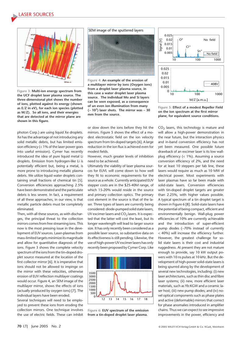
photon Corp.) are using liquid Xe droplets. Xe has the advantage of not introducing any solid metallic debris, but has limited emis-sion efficiency (< 1% of the laser power goes into useful emission). Cymer has recently introduced the idea of pure liquid metal Li droplets. Emission from hydrogen-like Li is potentially efficient but, being a metal, is more prone to introducing metallic plasma debris. We utilize liquid water droplets con-taining small fractions of chemical tin [5]. Conversion efficiencies approaching 2.5% have been demonstrated and the particulate debris is less severe. In fact, a requirement of all these approaches, in our view, is that metallic particle debris must be completely eliminated. Then, with all these sources, as with dischar-ges, the principal threat to the collection mirrors comes from free streaming ions. This now is the most pressing issue in the deve-lopment of EUV sources. Laser-plasmas from mass-limited targets minimize its magnitude and allow for quantitative diagnosis of the ions. Figure 3 shows the complete velocity spectrum of the ions from the tin-doped dro-plet source measured at the location of the first collector mirror [6]. It is imperative that ions should not be allowed to impinge on the mirror with these velocities, otherwise erosion of EUV reflection multilayer coatings would occur. Figure 4, an SEM image of the multilayer mirror, shows the effects of ions (actually produced by oxygen ions) [7]. The individual layers have been eroded. Several techniques will need to be emplo-yed to prevent these ions from eroding the collection mirrors. One technique involves the use of electric fields. These can inhibit
Figure 3: Multi-ion energy spectrum from the UCF droplet laser plasma source. The three-dimensional plot shows the number of ions, plotted against its energy (shown as E/Z in eV), for each ion species (plotted as M/Z). So all ions, and their energies that are detected at the mirror plane are shown in this figure.
SEM image of the sputtered layers
Figure 4: An example of the erosion of a multilayer mirror by ions (Oxygen ions) from a droplet laser plasma source, in this case a water droplet laser plasma source. The individual Mo and Si layers can be seen exposed, as a consequence of un even ion illumination from many (~ 107) laser shots. The mirror was ~ 30 mm from the source.
O+
Cl +
Sn +
No field
0.0050.01
0.0150.02
0.025
10 100 1000
Sign
al[V
]
No field
O+
Cl+
Sn+
No field
00.005
0.010.0150.02
0.025
10 100 1000
M/Z [a.m.u.]
408V
Figure 5: Effect of a modest Repeller Field on the ion spectrum at the first mirror plane, for equivalent source conditions.
12 13 1 15 16 17 180500
100015002000250030003500
12 13 14 15 16 17 180
500100015002000250030003500
Figure 6: EUV spectrum of the emission from a tin-doped droplet laser plasma.

LASER SOURCES
www.laser-journal.de LTJ 71 © 2005 WILEY-VCH Verlag GmbH & Co. KGaA, Weinheim
[8] Simi A. George, Chiew-Seng Koay, Kazu-toshi Takenoshita, Robert Bernath, Moza Mohammad Al-Rabban, Christian Keyser, Vivek Bakshi, H. Scott, Martin C. Richard-son, EUV spectroscopy of mass-limited Sn-doped laser micro-plasmas, Procee-dings of SPIE, volume 5751, 2005.
ruggedness of these lasers over the next few years. Hopefully, we can also expect the ca-pital cost of these systems to reduce over the next few years, to levels where they are com-petitive in time for the introduction of EUV Lithography into computer chip fabrication, probably at the end of this decade.
This work was founded by Sematech and the state of Florida.
References[1] Y. Watanabe, K. Ota & H. Franken, Source
requirements, presentation at ISMT EUV source Workshop, Sept 29, 2003.
[2] Uwe Stamm, Extreme ultraviolet light source-State of the art, future develop-ments, and potential application; RIKEN Review No. 50; January, 2003.
[3] F. Jin, K. Gabel, M. Richardson, M. Kado, A.F. Vassiliev, and D. Salzmann, Mass-limited laser plasma cryogenic target for 13-nm point x-ray sources for lithogra-phy, Proc. SPIE, vol. 2015, pp. 151-159, (1993).
[4] We have just demonstrated 30 kHz irra-diation of a 30 kHz droplet stream with in intelligent automatic feedback system to ensure long-term target positioning precision to ~ 3 µm.
[5] Martin C. Richardson, Chiew-Seng Koay, Kazutoshi Takenoshita, Christian Keyser, High conversion efficiency mass-limited Sn-based laser plasma source for EUV lithography, Journal of Vacuum Science and Technology B, volume 22, number 2, pp. 785-790 (March 2004).
[6] Kazutoshi Takenoshita, Chiew-Seng Koay, Somsak Teerawattanasook, Martin C. Richardson, Debris characterization and mitigation from microscopic laser-plasma tin-doped droplet EUV sources, Proceedings of SPIE, volume 5751, 2005 (to be published).
[7] Guido Schriever, Christian Keyser, Martin C. Richardson, Debris-free, droplet loser plasma sources in the EUV and soft X-ray ranges, I.C.E. Turcu, International Quantum Electronics Conference, page 13, 10-15 July 2000.