Embed Size (px)
Citation preview

LCD TVSERVICE MANUAL
CAUTIONBEFORE SERVICING THE CHASSIS,READ THE SAFETY PRECAUTIONS IN THIS MANUAL.
CHASSIS : LD91A
MODEL : 32LG2100 32LG2100-ZA
North/Latin America http://aic.lgservice.comEurope/Africa http://eic.lgservice.comAsia/Oceania http://biz.lgservice.com
Printed in KoreaP/NO : MFL50326821 (0904-REV00)
Internal Use Only
LGE Internal Use OnlyCopyright ©2009 LG Electronics. Inc. All right reserved. Only for training and service purposes
- 2 -
CONTENTS
CONTENTS .............................................................................................. 2
PRODUCT SAFETY ................................................................................. 3
SPECIFICATION ....................................................................................... 6
ADJUSTMENT INSTRUCTION ................................................................ 9
EXPLODED VIEW .................................................................................. 14
SVC. SHEET ...............................................................................................
LGE Internal Use OnlyCopyright ©2009 LG Electronics. Inc. All right reserved. Only for training and service purposes
- 3 -
SAFETY PRECAUTIONS
Many electrical and mechanical parts in this chassis have special safety-related characteristics. These parts are identified by in theSchematic Diagram and Exploded View.It is essential that these special safety parts should be replaced with the same components as recommended in this manual to preventShock, Fire, or other Hazards. Do not modify the original design without permission of manufacturer.
General Guidance
An isolation Transformer should always be used during theservicing of a receiver whose chassis is not isolated from the ACpower line. Use a transformer of adequate power rating as thisprotects the technician from accidents resulting in personal injuryfrom electrical shocks.
It will also protect the receiver and it's components from beingdamaged by accidental shorts of the circuitry that may beinadvertently introduced during the service operation.
If any fuse (or Fusible Resistor) in this TV receiver is blown,replace it with the specified.
When replacing a high wattage resistor (Oxide Metal Film Resistor,over 1W), keep the resistor 10mm away from PCB.
Keep wires away from high voltage or high temperature parts.
Before returning the receiver to the customer,
always perform an AC leakage current check on the exposedmetallic parts of the cabinet, such as antennas, terminals, etc., tobe sure the set is safe to operate without damage of electricalshock.
Leakage Current Cold Check(Antenna Cold Check)With the instrument AC plug removed from AC source, connect anelectrical jumper across the two AC plug prongs. Place the ACswitch in the on position, connect one lead of ohm-meter to the ACplug prongs tied together and touch other ohm-meter lead in turn toeach exposed metallic parts such as antenna terminals, phonejacks, etc. If the exposed metallic part has a return path to the chassis, themeasured resistance should be between 1MΩ and 5.2MΩ. When the exposed metal has no return path to the chassis thereading must be infinite.An other abnormality exists that must be corrected before thereceiver is returned to the customer.
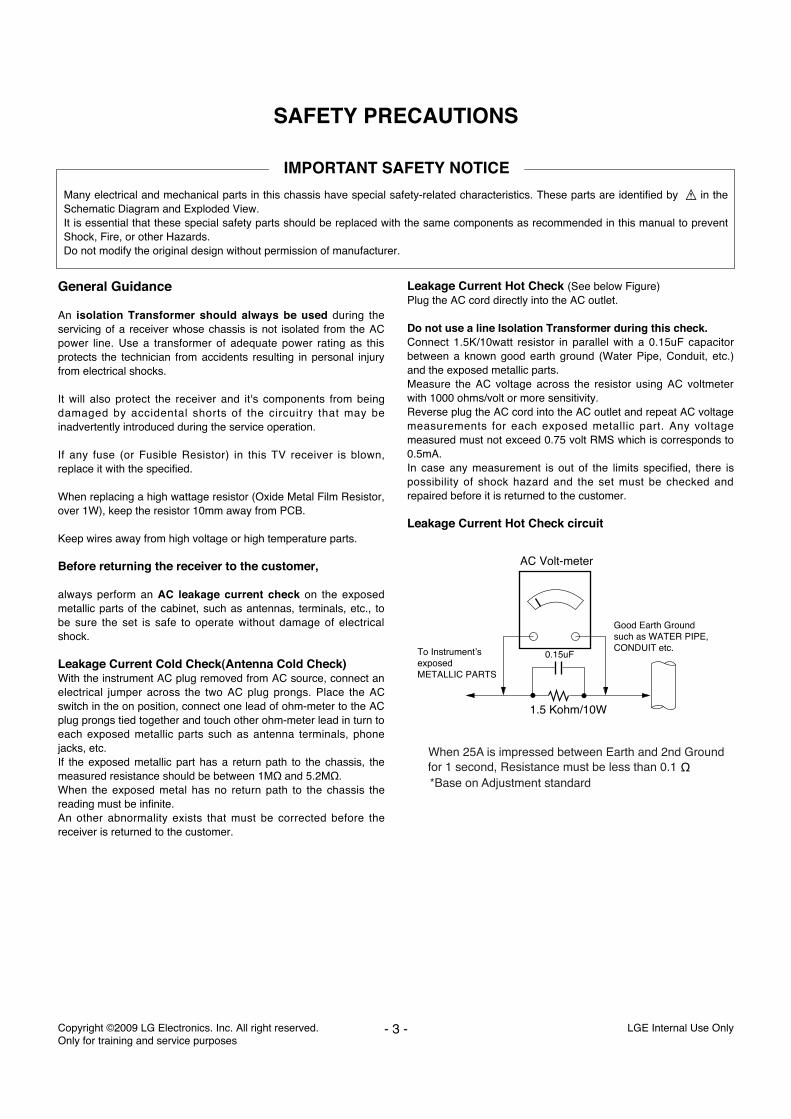
Leakage Current Hot Check (See below Figure) Plug the AC cord directly into the AC outlet.
Do not use a line Isolation Transformer during this check.Connect 1.5K/10watt resistor in parallel with a 0.15uF capacitorbetween a known good earth ground (Water Pipe, Conduit, etc.)and the exposed metallic parts.Measure the AC voltage across the resistor using AC voltmeterwith 1000 ohms/volt or more sensitivity.Reverse plug the AC cord into the AC outlet and repeat AC voltagemeasurements for each exposed metallic part. Any voltagemeasured must not exceed 0.75 volt RMS which is corresponds to0.5mA.In case any measurement is out of the limits specified, there ispossibility of shock hazard and the set must be checked andrepaired before it is returned to the customer.
Leakage Current Hot Check circuit
1.5 Kohm/10W
To Instrument’sexposed METALLIC PARTS
Good Earth Groundsuch as WATER PIPE,CONDUIT etc.
AC Volt-meter
When 25A is impressed between Earth and 2nd Groundfor 1 second, Resistance must be less than 0.1*Base on Adjustment standard
IMPORTANT SAFETY NOTICE
0.15uF
Ω
LGE Internal Use OnlyCopyright ©2009 LG Electronics. Inc. All right reserved. Only for training and service purposes
- 4 -
CAUTION: Before servicing receivers covered by this servicemanual and its supplements and addenda, read and follow theSAFETY PRECAUTIONS on page 3 of this publication.NOTE: If unforeseen circumstances create conflict between thefollowing servicing precautions and any of the safety precautions onpage 3 of this publication, always follow the safety precautions.Remember: Safety First.
General Servicing Precautions1. Always unplug the receiver AC power cord from the AC power
source before;a. Removing or reinstalling any component, circuit board
module or any other receiver assembly.b. Disconnecting or reconnecting any receiver electrical plug or
other electrical connection.c. Connecting a test substitute in parallel with an electrolytic
capacitor in the receiver.CAUTION: A wrong part substitution or incorrect polarityinstallation of electrolytic capacitors may result in anexplosion hazard.
2. Test high voltage only by measuring it with an appropriate highvoltage meter or other voltage measuring device (DVM,FETVOM, etc) equipped with a suitable high voltage probe.Do not test high voltage by "drawing an arc".
3. Do not spray chemicals on or near this receiver or any of itsassemblies.
4. Unless specified otherwise in this service manual, cleanelectrical contacts only by applying the following mixture to thecontacts with a pipe cleaner, cotton-tipped stick or comparablenon-abrasive applicator; 10% (by volume) Acetone and 90% (byvolume) isopropyl alcohol (90%-99% strength)CAUTION: This is a flammable mixture.Unless specified otherwise in this service manual, lubrication ofcontacts in not required.
5. Do not defeat any plug/socket B+ voltage interlocks with whichreceivers covered by this service manual might be equipped.
6. Do not apply AC power to this instrument and/or any of itselectrical assemblies unless all solid-state device heat sinks arecorrectly installed.
7. Always connect the test receiver ground lead to the receiverchassis ground before connecting the test receiver positivelead.Always remove the test receiver ground lead last.
8. Use with this receiver only the test fixtures specified in thisservice manual.CAUTION: Do not connect the test fixture ground strap to anyheat sink in this receiver.
Electrostatically Sensitive (ES) DevicesSome semiconductor (solid-state) devices can be damaged easilyby static electricity. Such components commonly are calledElectrostatically Sensitive (ES) Devices. Examples of typical ESdevices are integrated circuits and some field-effect transistors andsemiconductor "chip" components. The following techniquesshould be used to help reduce the incidence of componentdamage caused by static by static electricity.1. Immediately before handling any semiconductor component or
semiconductor-equipped assembly, drain off any electrostaticcharge on your body by touching a known earth ground.Alternatively, obtain and wear a commercially availabledischarging wrist strap device, which should be removed toprevent potential shock reasons prior to applying power to the
unit under test.2. After removing an electrical assembly equipped with ES
devices, place the assembly on a conductive surface such asaluminum foil, to prevent electrostatic charge buildup orexposure of the assembly.
3. Use only a grounded-tip soldering iron to solder or unsolder ESdevices.
4. Use only an anti-static type solder removal device. Some solderremoval devices not classified as "anti-static" can generateelectrical charges sufficient to damage ES devices.
5. Do not use freon-propelled chemicals. These can generateelectrical charges sufficient to damage ES devices.
6. Do not remove a replacement ES device from its protectivepackage until immediately before you are ready to install it.(Most replacement ES devices are packaged with leadselectrically shorted together by conductive foam, aluminum foilor comparable conductive material).
7. Immediately before removing the protective material from theleads of a replacement ES device, touch the protective materialto the chassis or circuit assembly into which the device will beinstalled.CAUTION: Be sure no power is applied to the chassis or circuit,and observe all other safety precautions.
8. Minimize bodily motions when handling unpackagedreplacement ES devices. (Otherwise harmless motion such asthe brushing together of your clothes fabric or the lifting of yourfoot from a carpeted floor can generate static electricitysufficient to damage an ES device.)
General Soldering Guidelines1. Use a grounded-tip, low-wattage soldering iron and appropriate
tip size and shape that will maintain tip temperature within therange or 500°F to 600°F.
2. Use an appropriate gauge of RMA resin-core solder composedof 60 parts tin/40 parts lead.
3. Keep the soldering iron tip clean and well tinned.4. Thoroughly clean the surfaces to be soldered. Use a mall wire-
bristle (0.5 inch, or 1.25cm) brush with a metal handle.Do not use freon-propelled spray-on cleaners.
5. Use the following unsoldering techniquea. Allow the soldering iron tip to reach normal temperature.
(500°F to 600°F)b. Heat the component lead until the solder melts.c. Quickly draw the melted solder with an anti-static, suction-
type solder removal device or with solder braid.CAUTION: Work quickly to avoid overheating the circuitboard printed foil.
6. Use the following soldering technique.a. Allow the soldering iron tip to reach a normal temperature
(500°F to 600°F)b. First, hold the soldering iron tip and solder the strand against
the component lead until the solder melts.c. Quickly move the soldering iron tip to the junction of the
component lead and the printed circuit foil, and hold it thereonly until the solder flows onto and around both thecomponent lead and the foil.CAUTION: Work quickly to avoid overheating the circuitboard printed foil.
d. Closely inspect the solder area and remove any excess orsplashed solder with a small wire-bristle brush.
SERVICING PRECAUTIONS
LGE Internal Use OnlyCopyright ©2009 LG Electronics. Inc. All right reserved. Only for training and service purposes
- 5 -
IC Remove/ReplacementSome chassis circuit boards have slotted holes (oblong) throughwhich the IC leads are inserted and then bent flat against thecircuit foil. When holes are the slotted type, the following techniqueshould be used to remove and replace the IC. When working withboards using the familiar round hole, use the standard techniqueas outlined in paragraphs 5 and 6 above.
Removal1. Desolder and straighten each IC lead in one operation by gently
prying up on the lead with the soldering iron tip as the soldermelts.
2. Draw away the melted solder with an anti-static suction-typesolder removal device (or with solder braid) before removing theIC.
Replacement1. Carefully insert the replacement IC in the circuit board.2. Carefully bend each IC lead against the circuit foil pad and
solder it.3. Clean the soldered areas with a small wire-bristle brush.
(It is not necessary to reapply acrylic coating to the areas).
"Small-Signal" Discrete TransistorRemoval/Replacement1. Remove the defective transistor by clipping its leads as close as
possible to the component body.2. Bend into a "U" shape the end of each of three leads remaining
on the circuit board.3. Bend into a "U" shape the replacement transistor leads.4. Connect the replacement transistor leads to the corresponding
leads extending from the circuit board and crimp the "U" withlong nose pliers to insure metal to metal contact then soldereach connection.
Power Output, Transistor DeviceRemoval/Replacement1. Heat and remove all solder from around the transistor leads.2. Remove the heat sink mounting screw (if so equipped).3. Carefully remove the transistor from the heat sink of the circuit
board.4. Insert new transistor in the circuit board.5. Solder each transistor lead, and clip off excess lead.6. Replace heat sink.
Diode Removal/Replacement1. Remove defective diode by clipping its leads as close as
possible to diode body.2. Bend the two remaining leads perpendicular y to the circuit
board.3. Observing diode polarity, wrap each lead of the new diode
around the corresponding lead on the circuit board.4. Securely crimp each connection and solder it.5. Inspect (on the circuit board copper side) the solder joints of
the two "original" leads. If they are not shiny, reheat them and ifnecessary, apply additional solder.
Fuse and Conventional ResistorRemoval/Replacement1. Clip each fuse or resistor lead at top of the circuit board hollow
stake.2. Securely crimp the leads of replacement component around
notch at stake top.3. Solder the connections.
CAUTION: Maintain original spacing between the replacedcomponent and adjacent components and the circuit board toprevent excessive component temperatures.
Circuit Board Foil RepairExcessive heat applied to the copper foil of any printed circuitboard will weaken the adhesive that bonds the foil to the circuitboard causing the foil to separate from or "lift-off" the board. Thefollowing guidelines and procedures should be followed wheneverthis condition is encountered.
At IC ConnectionsTo repair a defective copper pattern at IC connections use thefollowing procedure to install a jumper wire on the copper patternside of the circuit board. (Use this technique only on ICconnections).
1. Carefully remove the damaged copper pattern with a sharpknife. (Remove only as much copper as absolutely necessary).
2. carefully scratch away the solder resist and acrylic coating (ifused) from the end of the remaining copper pattern.
3. Bend a small "U" in one end of a small gauge jumper wire andcarefully crimp it around the IC pin. Solder the IC connection.
4. Route the jumper wire along the path of the out-away copperpattern and let it overlap the previously scraped end of the goodcopper pattern. Solder the overlapped area and clip off anyexcess jumper wire.
At Other ConnectionsUse the following technique to repair the defective copper patternat connections other than IC Pins. This technique involves theinstallation of a jumper wire on the component side of the circuitboard.
1. Remove the defective copper pattern with a sharp knife.Remove at least 1/4 inch of copper, to ensure that a hazardouscondition will not exist if the jumper wire opens.
2. Trace along the copper pattern from both sides of the patternbreak and locate the nearest component that is directlyconnected to the affected copper pattern.
3. Connect insulated 20-gauge jumper wire from the lead of thenearest component on one side of the pattern break to the leadof the nearest component on the other side.Carefully crimp and solder the connections.CAUTION: Be sure the insulated jumper wire is dressed so theit does not touch components or sharp edges.
LGE Internal Use OnlyCopyright ©2009 LG Electronics. Inc. All right reserved. Only for training and service purposes
- 6 -
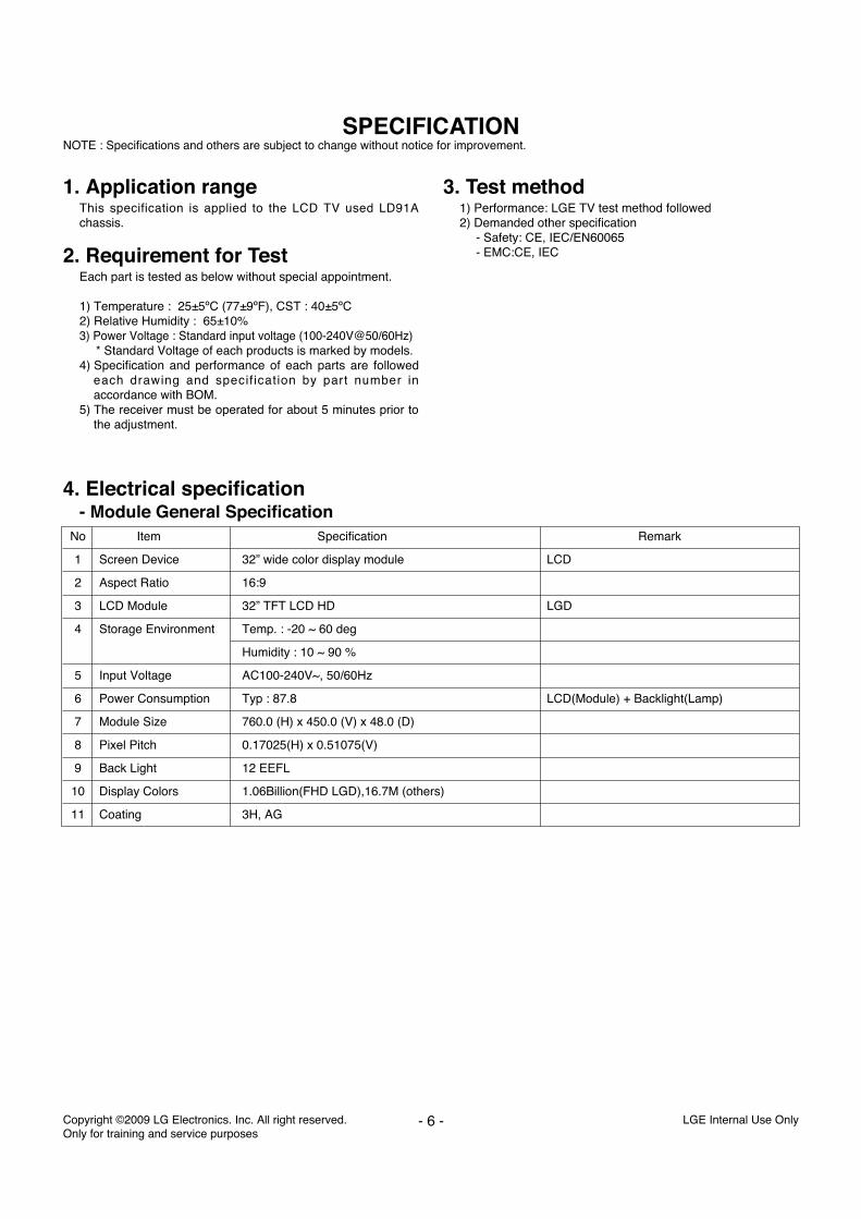
SPECIFICATIONNOTE : Specifications and others are subject to change without notice for improvement.
4. Electrical specification- Module General Specification
1. Application rangeThis specification is applied to the LCD TV used LD91Achassis.
2. Requirement for TestEach part is tested as below without special appointment.
1) Temperature : 25±5ºC (77±9ºF), CST : 40±5ºC2) Relative Humidity : 65±10%3) Power Voltage : Standard input voltage (100-240V@50/60Hz)
* Standard Voltage of each products is marked by models.4) Specification and performance of each parts are followed
each drawing and specif ication by part number inaccordance with BOM.
5) The receiver must be operated for about 5 minutes prior tothe adjustment.
3. Test method1) Performance: LGE TV test method followed 2) Demanded other specification
- Safety: CE, IEC/EN60065- EMC:CE, IEC
No Item Specification Remark
1 Screen Device 32” wide color display module LCD
2 Aspect Ratio 16:9
3 LCD Module 32” TFT LCD HD LGD
4 Storage Environment Temp. : -20 ~ 60 deg
Humidity : 10 ~ 90 %
5 Input Voltage AC100-240V~, 50/60Hz
6 Power Consumption Typ : 87.8 LCD(Module) + Backlight(Lamp)
7 Module Size 760.0 (H) x 450.0 (V) x 48.0 (D)
8 Pixel Pitch 0.17025(H) x 0.51075(V)
9 Back Light 12 EEFL
10 Display Colors 1.06Billion(FHD LGD),16.7M (others)
11 Coating 3H, AG
- 7 - LGE Internal Use OnlyCopyright ©2009 LG Electronics. Inc. All right reserved. Only for training and service purposes
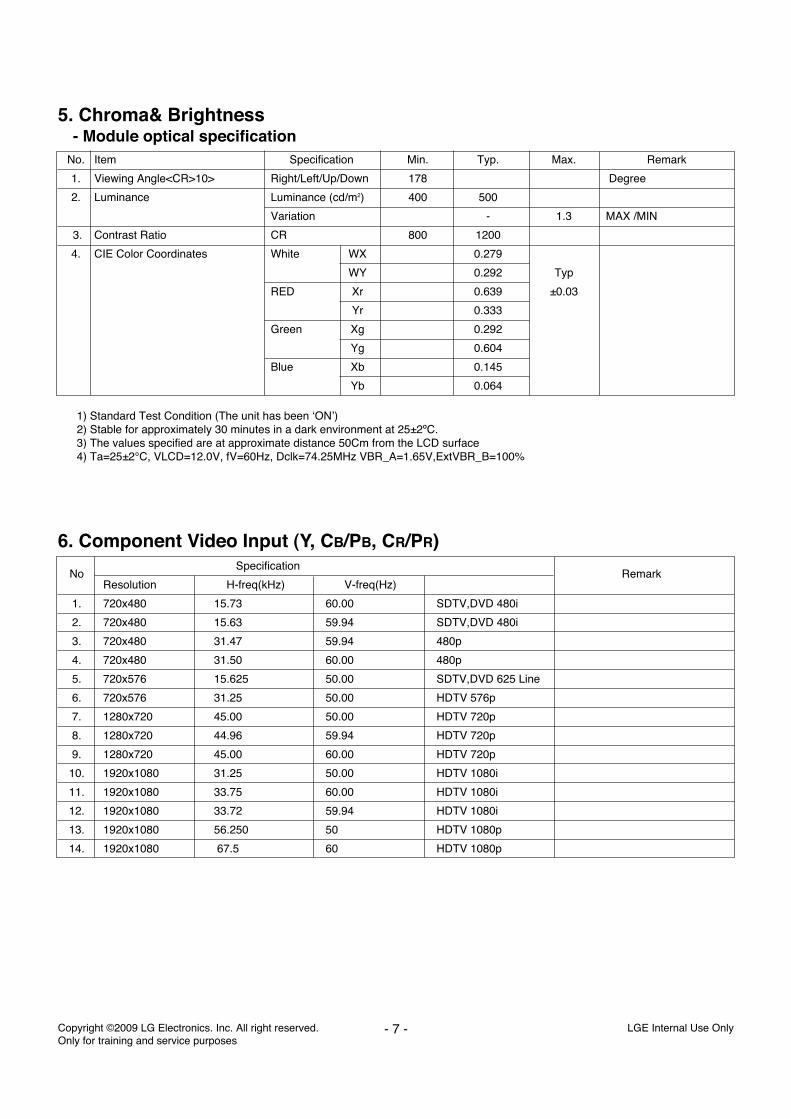
5. Chroma& Brightness- Module optical specification
1) Standard Test Condition (The unit has been ‘ON’)2) Stable for approximately 30 minutes in a dark environment at 25±2ºC.3) The values specified are at approximate distance 50Cm from the LCD surface4) Ta=25±2°C, VLCD=12.0V, fV=60Hz, Dclk=74.25MHz VBR_A=1.65V,ExtVBR_B=100%
No. Item Specification Min. Typ. Max. Remark
1. Viewing Angle<CR>10> Right/Left/Up/Down 178 Degree
2. Luminance Luminance (cd/m2) 400 500
Variation - 1.3 MAX /MIN
3. Contrast Ratio CR 800 1200
4. CIE Color Coordinates White WX 0.279
WY 0.292 Typ
RED Xr 0.639 ±0.03
Yr 0.333
Green Xg 0.292
Yg 0.604
Blue Xb 0.145
Yb 0.064
6. Component Video Input (Y, CB/PB, CR/PR)
NoSpecification
RemarkResolution H-freq(kHz) V-freq(Hz)
1. 720x480 15.73 60.00 SDTV,DVD 480i
2. 720x480 15.63 59.94 SDTV,DVD 480i
3. 720x480 31.47 59.94 480p
4. 720x480 31.50 60.00 480p
5. 720x576 15.625 50.00 SDTV,DVD 625 Line
6. 720x576 31.25 50.00 HDTV 576p
7. 1280x720 45.00 50.00 HDTV 720p
8. 1280x720 44.96 59.94 HDTV 720p
9. 1280x720 45.00 60.00 HDTV 720p
10. 1920x1080 31.25 50.00 HDTV 1080i
11. 1920x1080 33.75 60.00 HDTV 1080i
12. 1920x1080 33.72 59.94 HDTV 1080i
13. 1920x1080 56.250 50 HDTV 1080p
14. 1920x1080 67.5 60 HDTV 1080p
- 8 - LGE Internal Use OnlyCopyright ©2009 LG Electronics. Inc. All right reserved. Only for training and service purposes
NoSpecification
Proposed RemarkResolution H-freq(kHz) V-freq(Hz) Pixel Clock(MHz)
1. 720*400 31.468 70.08 28.321 For only DOS mode
2. 640*480 31.469 59.94 25.17 VESA Input 848*480 60Hz, 852*480 60Hz
-> 640*480 60Hz Display
3. 800*600 37.879 60.31 40.00 VESA
4. 1024*768 48.363 60.00 65.00 VESA(XGA)
5. 1280*768 47.78 59.87 79.5 WXGA
6. 1360*768 47.72 59.8 84.75 WXGA
7. 1280*1024 63.595 60.0 108.875 SXGA FHD model
8. 1920*1080 66.587 59.93 138.625 WUXGA FHD model
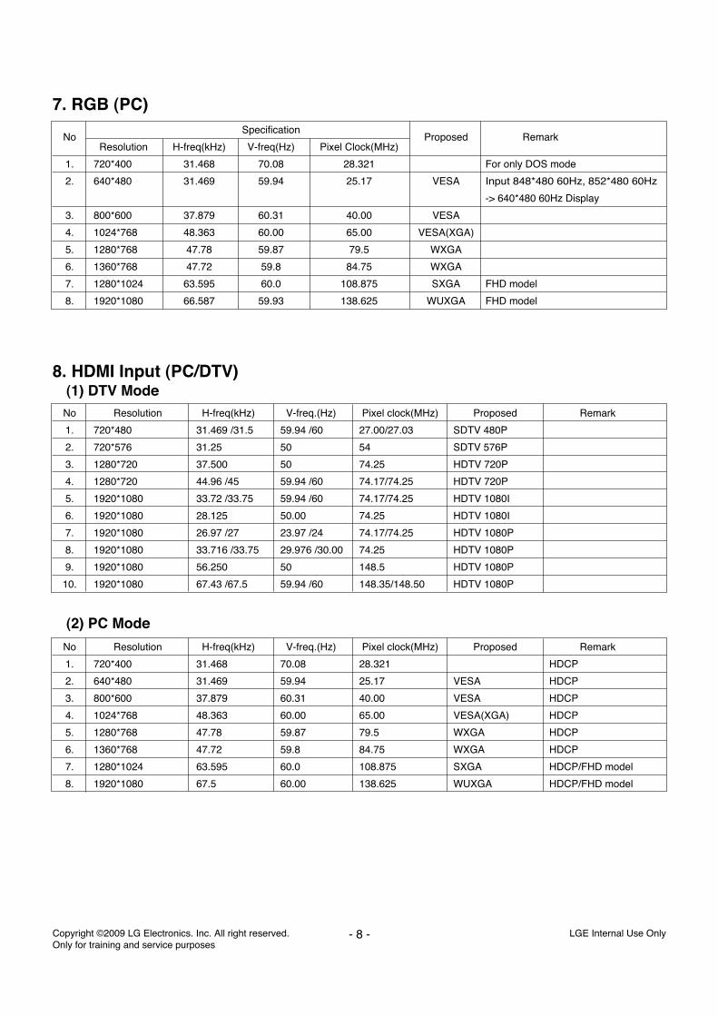
7. RGB (PC)
8. HDMI Input (PC/DTV)(1) DTV Mode
No Resolution H-freq(kHz) V-freq.(Hz) Pixel clock(MHz) Proposed Remark
1. 720*400 31.468 70.08 28.321 HDCP
2. 640*480 31.469 59.94 25.17 VESA HDCP
3. 800*600 37.879 60.31 40.00 VESA HDCP
4. 1024*768 48.363 60.00 65.00 VESA(XGA) HDCP
5. 1280*768 47.78 59.87 79.5 WXGA HDCP
6. 1360*768 47.72 59.8 84.75 WXGA HDCP
7. 1280*1024 63.595 60.0 108.875 SXGA HDCP/FHD model
8. 1920*1080 67.5 60.00 138.625 WUXGA HDCP/FHD model
(2) PC Mode
No Resolution H-freq(kHz) V-freq.(Hz) Pixel clock(MHz) Proposed Remark
1. 720*480 31.469 /31.5 59.94 /60 27.00/27.03 SDTV 480P
2. 720*576 31.25 50 54 SDTV 576P
3. 1280*720 37.500 50 74.25 HDTV 720P
4. 1280*720 44.96 /45 59.94 /60 74.17/74.25 HDTV 720P
5. 1920*1080 33.72 /33.75 59.94 /60 74.17/74.25 HDTV 1080I
6. 1920*1080 28.125 50.00 74.25 HDTV 1080I
7. 1920*1080 26.97 /27 23.97 /24 74.17/74.25 HDTV 1080P
8. 1920*1080 33.716 /33.75 29.976 /30.00 74.25 HDTV 1080P
9. 1920*1080 56.250 50 148.5 HDTV 1080P
10. 1920*1080 67.43 /67.5 59.94 /60 148.35/148.50 HDTV 1080P
LGE Internal Use OnlyCopyright ©2009 LG Electronics. Inc. All right reserved. Only for training and service purposes
- 9 -
ADJUSTMENT INSTRUCTION
1. Application RangeThis specification sheet is applied to all of the LCD TV withLD91A chassis.
2. Designation1) The adjustment is according to the order which is
designated and which must be followed, according to theplan which can be changed only on agreeing.
2) Power Adjustment: Free Voltage3) Magnetic Field Condition: Nil.4) Input signal Unit: Product Specification Standard5) Reserve after operation: Above 5 Minutes (Heat Run)
Temperature : at 25±5ºC Relative humidity : 65±10%Input voltage : 220V, 60Hz
6) Adjustment equipments: Color Analyzer (CA-210 or CA-110), DDC Adjustment Jig equipment, SVC remotecontroller
7) Push The “IN STOP KEY” - For memory initialization.
3. Main PCB check process* APC - After Manual-Insult, executing APC
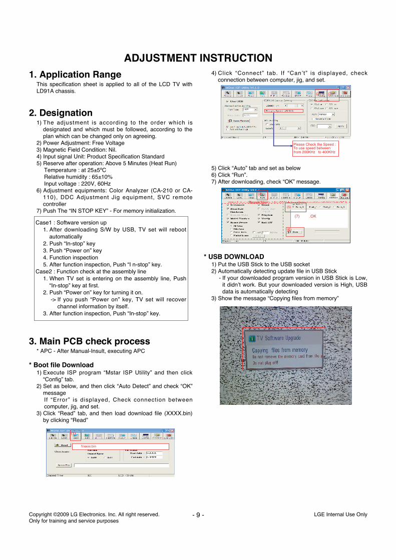
* Boot file Download1) Execute ISP program “Mstar ISP Utility” and then click
“Config” tab.2) Set as below, and then click “Auto Detect” and check “OK”
messageIf “Error” is displayed, Check connection betweencomputer, jig, and set.
3) Click “Read” tab, and then load download file (XXXX.bin)by clicking “Read”
4) Click “Connect” tab. If “Can’t” is displayed, checkconnection between computer, jig, and set.
5) Click “Auto” tab and set as below6) Click “Run”.7) After downloading, check “OK” message.
* USB DOWNLOAD1) Put the USB Stick to the USB socket 2) Automatically detecting update file in USB Stick
- If your downloaded program version in USB Stick is Low,it didn’t work. But your downloaded version is High, USBdata is automatically detecting
3) Show the message “Copying files from memory”
filexxx.bin
(4)
(7) .OK
(5)
(6)
(1)
fi lexxx.bin
(2) (3)
Please Check the Speed : To use speed between from 200KHz to 400KHz
Case1 : Software version up1. After downloading S/W by USB, TV set will reboot
automatically2. Push “In-stop” key3. Push “Power on” key4. Function inspection5. After function inspection, Push “I n-stop” key.
Case2 : Function check at the assembly line1. When TV set is entering on the assembly line, Push
“In-stop” key at first.2. Push “Power on” key for turning it on.
-> If you push “Power on” key, TV set will recoverchannel information by itself.
3. After function inspection, Push “In-stop” key.
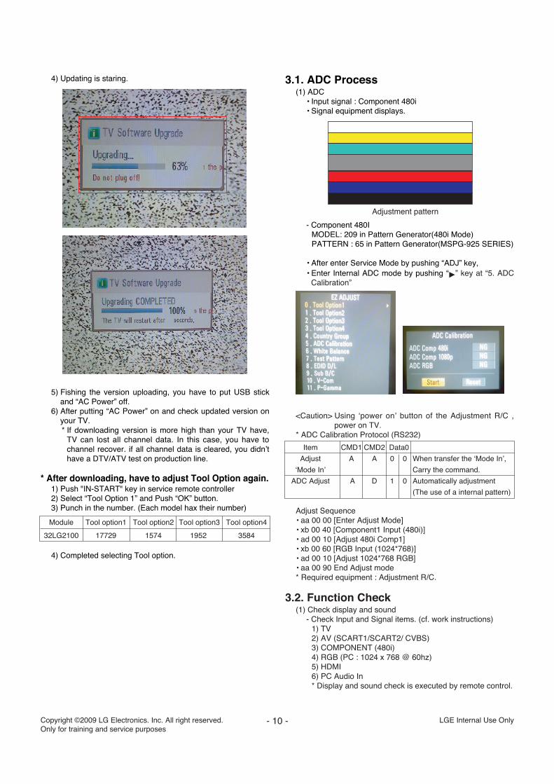
4) Updating is staring.
5) Fishing the version uploading, you have to put USB stickand “AC Power” off.
6) After putting “AC Power” on and check updated version onyour TV.* If downloading version is more high than your TV have,
TV can lost all channel data. In this case, you have tochannel recover. if all channel data is cleared, you didn’thave a DTV/ATV test on production line.
* After downloading, have to adjust Tool Option again.1) Push "IN-START" key in service remote controller 2) Select “Tool Option 1” and Push “OK” button.3) Punch in the number. (Each model hax their number)
4) Completed selecting Tool option.
3.1. ADC Process(1) ADC
• Input signal : Component 480i• Signal equipment displays.
- Component 480IMODEL: 209 in Pattern Generator(480i Mode)PATTERN : 65 in Pattern Generator(MSPG-925 SERIES)
• After enter Service Mode by pushing “ADJ” key,• Enter Internal ADC mode by pushing “G” key at “5. ADC
Calibration”
<Caution> Using ‘power on’ button of the Adjustment R/C ,power on TV.
* ADC Calibration Protocol (RS232)
Adjust Sequence• aa 00 00 [Enter Adjust Mode]• xb 00 40 [Component1 Input (480i)]• ad 00 10 [Adjust 480i Comp1]• xb 00 60 [RGB Input (1024*768)]• ad 00 10 [Adjust 1024*768 RGB]• aa 00 90 End Adjust mode* Required equipment : Adjustment R/C.
3.2. Function Check(1) Check display and sound
- Check Input and Signal items. (cf. work instructions)1) TV2) AV (SCART1/SCART2/ CVBS)3) COMPONENT (480i)4) RGB (PC : 1024 x 768 @ 60hz)5) HDMI6) PC Audio In* Display and sound check is executed by remote control.
- 10 - LGE Internal Use OnlyCopyright ©2009 LG Electronics. Inc. All right reserved. Only for training and service purposes
Module Tool option1 Tool option2 Tool option3 Tool option4
32LG2100 17729 1574 1952 3584
Item CMD1 CMD2 Data0
Adjust A A 0 0 When transfer the ‘Mode In’,
‘Mode In’ Carry the command.
ADC Adjust A D 1 0 Automatically adjustment
(The use of a internal pattern)
Adjustment pattern
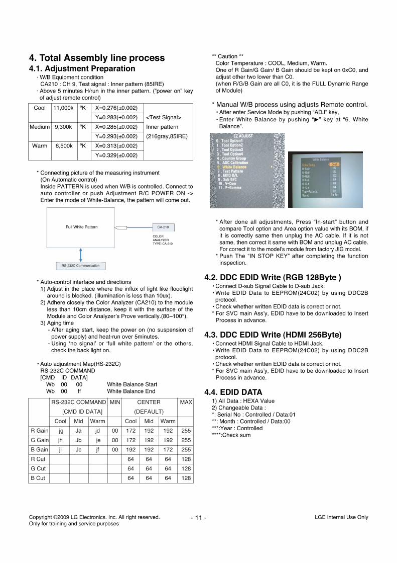
4. Total Assembly line process4.1. Adjustment Preparation
· W/B Equipment conditionCA210 : CH 9, Test signal : Inner pattern (85IRE)
· Above 5 minutes H/run in the inner pattern. (“power on” keyof adjust remote control)
* Connecting picture of the measuring instrument(On Automatic control)Inside PATTERN is used when W/B is controlled. Connect toauto controller or push Adjustment R/C POWER ON ->Enter the mode of White-Balance, the pattern will come out.
* Auto-control interface and directions1) Adjust in the place where the influx of light like floodlight
around is blocked. (illumination is less than 10ux).2) Adhere closely the Color Analyzer (CA210) to the module
less than 10cm distance, keep it with the surface of theModule and Color Analyzer’s Prove vertically.(80~100°).
3) Aging time- After aging start, keep the power on (no suspension of
power supply) and heat-run over 5minutes.- Using ‘no signal’ or ‘full white pattern’ or the others,
check the back light on.
• Auto adjustment Map(RS-232C)RS-232C COMMAND[CMD ID DATA]
Wb 00 00 White Balance StartWb 00 ff White Balance End
** Caution **Color Temperature : COOL, Medium, Warm. One of R Gain/G Gain/ B Gain should be kept on 0xC0, andadjust other two lower than C0.(when R/G/B Gain are all C0, it is the FULL Dynamic Rangeof Module)
* Manual W/B process using adjusts Remote control.• After enter Service Mode by pushing “ADJ” key,• Enter White Balance by pushing “G” key at “6. White
Balance”.
* After done all adjustments, Press “In-start” button andcompare Tool option and Area option value with its BOM, ifit is correctly same then unplug the AC cable. If it is notsame, then correct it same with BOM and unplug AC cable.For correct it to the model’s module from factory JIG model.
* Push The “IN STOP KEY” after completing the functioninspection.
4.2. DDC EDID Write (RGB 128Byte )• Connect D-sub Signal Cable to D-sub Jack.• Write EDID Data to EEPROM(24C02) by using DDC2B
protocol.• Check whether written EDID data is correct or not.* For SVC main Ass’y, EDID have to be downloaded to Insert
Process in advance.
4.3. DDC EDID Write (HDMI 256Byte)• Connect HDMI Signal Cable to HDMI Jack.• Write EDID Data to EEPROM(24C02) by using DDC2B
protocol.• Check whether written EDID data is correct or not.* For SVC main Ass’y, EDID have to be downloaded to Insert
Process in advance.
4.4. EDID DATA1) All Data : HEXA Value2) Changeable Data :*: Serial No : Controlled / Data:01**: Month : Controlled / Data:00***:Year : Controlled****:Check sum
- 11 - LGE Internal Use OnlyCopyright ©2009 LG Electronics. Inc. All right reserved. Only for training and service purposes
Cool 11,000k ºK X=0.276(±0.002)
Y=0.283(±0.002) <Test Signal>
Medium 9,300k ºK X=0.285(±0.002) Inner pattern
Y=0.293(±0.002) (216gray,85IRE)
Warm 6,500k ºK X=0.313(±0.002)
Y=0.329(±0.002)
Full White Pattern
COLORANALYZERTYPE: CA-210
RS-232C Communication
CA-210
RS-232C COMMAND MIN CENTER MAX
[CMD ID DATA] (DEFAULT)
Cool Mid Warm Cool Mid Warm
R Gain jg Ja jd 00 172 192 192 255
G Gain jh Jb je 00 172 192 192 255
B Gain ji Jc jf 00 192 192 172 255
R Cut 64 64 64 128
G Cut 64 64 64 128
B Cut 64 64 64 128
- Auto Download• After enter Service Mode by pushing “ADJ” key,• Enter EDID D/L mode.• Enter “START” by pushing “OK” key.
* Edid data and Model option download (RS232)
- Manual Download* Caution
1) Use the proper signal cable for EDID Download- Analog EDID : Pin3 exists- Digital EDID : Pin3 exists
2) Never connect HDMI & D-sub Cable at the same time.3) Use the proper cables below for EDID Writing4) Download HDMI1, HDMI2, separately because HDMI1 is
different from HDMI3
1) HD RGB EDID data
2) HD HDMI EDID data
* Detail EDID Options are below Product ID
Serial No: Controlled on production line.
Month, Year: Controlled on production line:ex) Monthly : ‘02’ -> ‘02’
Year : ‘2009’ -> ‘13’ Model Name(Hex):
Checksum: Changeable by total EDID data.
Vendor Specific(HDMI)
Model Name HEX EDID Table DDC Function
FHD Model 0001 01 00 Analog/Digital
HD Model 0000 00 00 Analog/Digital
LGE Internal Use OnlyCopyright ©2009 LG Electronics. Inc. All right reserved. Only for training and service purposes
- 12 -
MODEL MODEL NAME(HEX)
all 00 00 00 FC 00 4C 47 20 54 56 0A 20 20 20 20 20 20 20
Item CMD1 CMD2 Data0
Download A A 0 0 When transfer the ‘Mode In’,
‘Mode In’ Carry the command.
Download A E 00 10 Automatically Download
(The use of a internal pattern)
Item
Manufacturer ID
Version
Revision
Condition
GSM
Digital : 1
Digital : 3
Data(Hex)
1E6D
01
03
D-sub to D-sub DVI-D to HDMI or HDMI to HDMI
For HDMI EDIDFor Analog EDID
0 1 2 3 4 5 6 7 8 9 A B C D E F00 00 F F F F F F F F F F F F 00 1E 6D a b10 c 01 03 80 73 41 78 0A C F 74 A3 57 4C B0 2320 09 48 4C A1 08 00 81 C0 61 40 45 40 31 40 01 0130 01 01 01 01 01 01 66 21 50 B0 51 00 1B 30 40 7040 36 00 7E 8A 42 00 00 1E 01 1D 00 72 51 D0 1E 2050 6E 28 55 00 7E 8A 42 00 00 1E 00 00 00 FD 00 3A60 3E 1F 46 10 00 0A 20 20 20 20 20 20 d70 d 01 e80 02 03 20 F1 4E 10 1F 84 13 05 14 03 02 12 20 2190 22 15 01 26 15 07 50 09 57 07 fA 0 f 80 18 71 1C 16 20 58 2C 25 00 7E 8A 42 00B0 00 9E 01 1D 00 80 51 D0 0C 20 40 80 35 00 7E 8AC0 42 00 00 1E 8C 0A D0 8A 20 E0 2D 10 10 3E 96 00D0 7E 8A 42 00 00 18 02 3A 80 18 71 38 2D 40 58 2CE0 45 00 7E 8A 42 00 00 1E 01 1D 80 D0 72 1C 16 20F0 10 2C 25 80 7E 8A 42 00 00 9E 00 00 00 00 00 D5
0 1 2 3 4 5 6 7 8 9 A B C D E F00 00 F F F F F F F F F F F F 00 1E 6D a b10 c 01 03 68 73 41 78 0A C F 74 A3 57 4C B0 2320 09 48 4C A1 08 00 81 C0 61 40 45 40 31 40 01 0130 01 01 01 01 01 01 66 21 50 B0 51 00 1B 30 40 7040 36 00 7E 8A 42 00 00 1E 01 1D 00 72 51 D0 1E 2050 6E 28 55 00 7E 8A 42 00 00 1E 00 00 00 FD 00 3A60 3E 1F 46 10 00 0A 20 20 20 20 20 20 d70 d 00 e80 F F F F F F F F F F F F F F F F F F F F F F F F F F F F F F F F90 F F F F F F F F F F F F F F F F F F F F F F F F F F F F F F F FA 0 F F F F F F F F F F F F F F F F F F F F F F F F F F F F F F F FB0 F F F F F F F F F F F F F F F F F F F F F F F F F F F F F F F FC0 F F F F F F F F F F F F F F F F F F F F F F F F F F F F F F F FD0 F F F F F F F F F F F F F F F F F F F F F F F F F F F F F F F FE0 F F F F F F F F F F F F F F F F F F F F F F F F F F F F F F F FF0 F F F F F F F F F F F F F F F F F F F F F F F F F F F F F F F F
INPUT MODEL NAME(HEX)
HDMI1 67030C001000011D
HDMI2 67030C002000011D
HDMI3 67030C003000011D
- 13 - LGE Internal Use OnlyCopyright ©2009 LG Electronics. Inc. All right reserved. Only for training and service purposes
4.5. Outgoing condition Configuration- When pressing IN-STOP key by SVC remocon, Red LED are
blinked alternatively. And then Automatically turn off.(Must not AC power OFF during blinking)
4.6. Internal pressureConfirm whether is normal or not when between powerboard’s ac block and GND is impacted on 1.5kV(dc) or2.2kV(dc) for one second
5. Model name & Serial number D/L• press “Power on” key of service remocon.
(Baud rate : 115200 bps)• Connect RS232 Signal Cable to RS-232 Jack.• Write Serial number by use RS-232.• Must check the serial number at the Diagnostics of SET UP
menu. (Refer to below).
5.1. Signal TABLE
CMD : A0hLENGTH : 85~94h (1~16 bytes)ADH : EEPROM Sub Address high (00~1F)ADL : EEPROM Sub Address low (00~FF)Data : Write dataCS : CMD + LENGTH + ADH + ADL + Data_1 +…+ Data_nDelay : 20ms
5.2. Command Set
* DescriptionFOS Default write : <7mode data> writeVtotal, V_Frequency, Sync_Polarity, Htotal, Hstart, Vstart, 0,PhaseData write : Model Name and Serial Number write in
EEPROM,.
5.3. Method & notice1) Serial number D/L is using of scan equipment.2) Setting of scan equipment operated by Manufacturing
Technology Group.3) Serial number D/L must be conformed when it is produced
in production line, because serial number D/L is mandatoryby D-book 4.0.
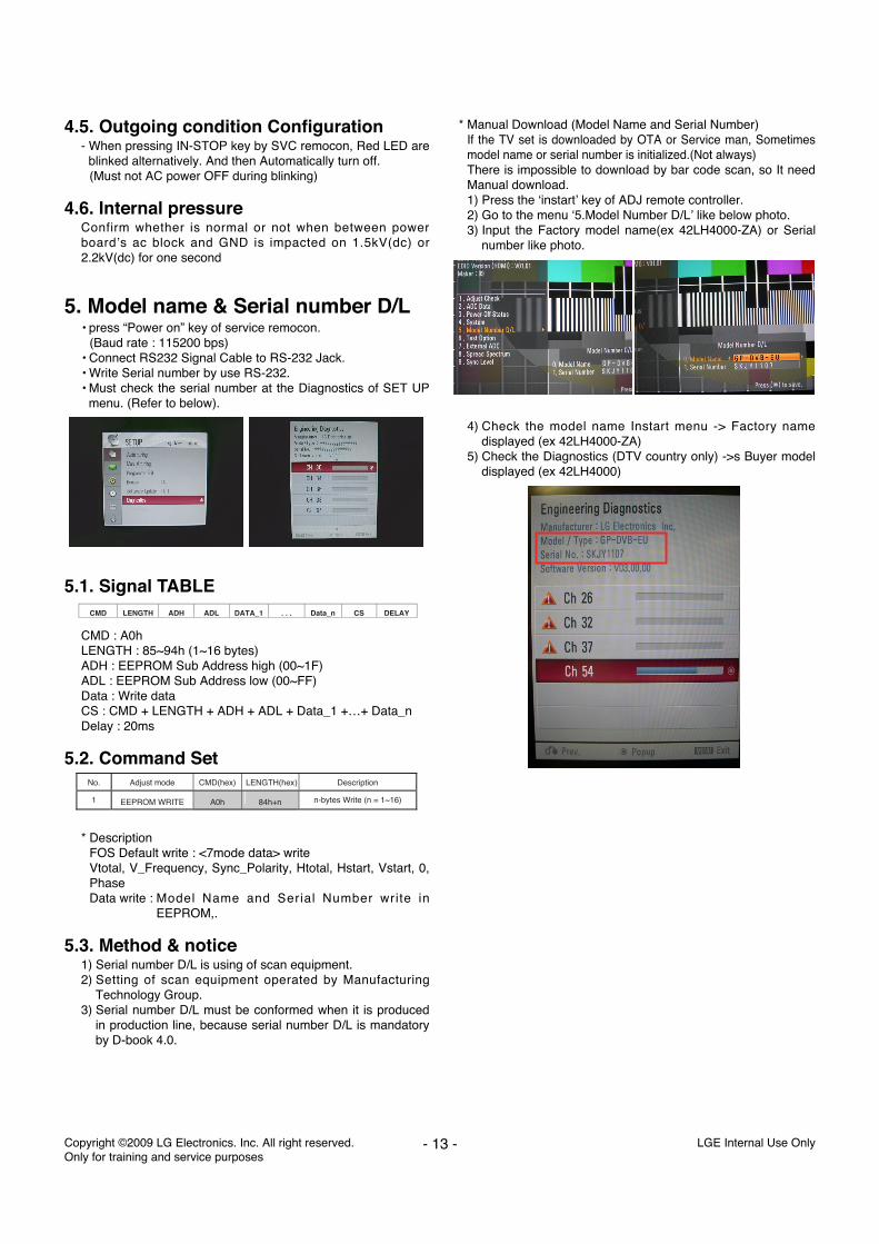
* Manual Download (Model Name and Serial Number)If the TV set is downloaded by OTA or Service man, Sometimesmodel name or serial number is initialized.(Not always)There is impossible to download by bar code scan, so It needManual download.1) Press the ‘instart’ key of ADJ remote controller.2) Go to the menu ‘5.Model Number D/L’ like below photo.3) Input the Factory model name(ex 42LH4000-ZA) or Serial
number like photo.
4) Check the model name Instart menu -> Factory namedisplayed (ex 42LH4000-ZA)
5) Check the Diagnostics (DTV country only) ->s Buyer modeldisplayed (ex 42LH4000)
CMD LENGTH ADH ADL DATA_1 . . . Data_n CS DELAY
No. Adjust mode CMD(hex) LENGTH(hex) Description
1 EEPROM WRITE A0h 84h+n n-bytes Write (n = 1~16)
- 14 - LGE Internal Use OnlyCopyright LG Electronics. Inc. All right reserved. Only for training and service purposes
300
200
200T
200N
120 12
2
400
500
510
521
530
540
550
801
805
802
804
803
800
821
900
910
LV1
A2
A10
A9
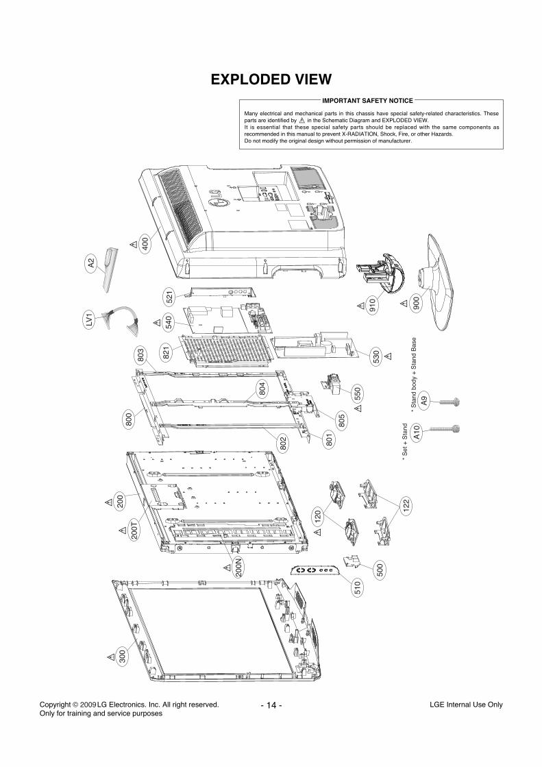
EXPLODED VIEW
Many electrical and mechanical parts in this chassis have special safety-related characteristics. Theseparts are identified by in the Schematic Diagram and EXPLODED VIEW. It is essential that these special safety parts should be replaced with the same components asrecommended in this manual to prevent X-RADIATION, Shock, Fire, or other Hazards. Do not modify the original design without permission of manufacturer.
IMPORTANT SAFETY NOTICE
THE
S
YMBO
L M
ARK
OF
THIS
SCH
EMET
IC D
IAG
RAM
INCO
RPO
RATE
SSP
ECIA
L FE
ATUR
ES IM
PORT
ANT
FOR
PRO
TECT
ION
FRO
M X
-RAD
IATI
ON.
FILR
E AN
D EL
ECTR
ICAL
SHO
CK H
AZAR
DS, W
HEN
SERV
ICIN
G IF
IS
ESSE
NTIA
L TH
AT O
NLY
MAN
UFAT
URES
SPE
CFIE
D PA
RTS
BE U
SED
FOR
THE
CRIT
ICAL
CO
MPO
NENT
S IN
THE
SYM
BOL
MAR
K O
F TH
E SC
HEM
ETIC
.
PC
M_
A[0
]
PC
M_
A[1
]
PC
M_
A[2
]
PC
M_
A[3
]
PC
M_
A[4
]
PC
M_
A[5
]
PC
M_
A[6
]
PC
M_
A[7
]
PC
M_
A[7
]
PC
M_
A[6
]
PC
M_
A[5
]
PC
M_
A[4
]
PC
M_
A[0
]
PC
M_
A[1
]
PC
M_
A[3
]
PC
M_
A[2
]
PC
M_
A[8
]
PC
M_
A[9
]
PC
M_
A[1
0]
PC
M_
A[1
2]
PC
M_
A[1
3]
PC
M_
A[1
1]
PC
M_
A[1
4]
PC
M_
D[0
]
PC
M_
D[1
]
PC
M_
D[2
]
PC
M_
D[3
]
PC
M_
D[4
]
PC
M_
D[5
]
PC
M_
D[6
]
PC
M_
D[7
]
CI_
TS
_D
AT
A[0
]
CI_
TS
_D
AT
A[1
]
CI_
TS
_D
AT
A[3
]
CI_
TS
_D
AT
A[2
]
CI_
TS
_D
AT
A[5
]
CI_
TS
_D
AT
A[4
]
CI_
TS
_D
AT
A[7
]
CI_
TS
_D
AT
A[6
]
ISP
_T
XD
EE
PR
OM
_S
DA
E2
0;T
19
;Y1
4
RE
AR
_U
SB
_D
M 4:A
J5
RE
AR
_U
SB
_D
P 4:A
J6
FE
_T
UN
ER
_S
DA
IC1
02
HY
27
US
08
12
1B
-TP
CB
26
NC
_1
7
27
NC
_1
8
28
NC
_1
9
29
I/O
0
30
I/O
1
31
I/O
2
32
I/O
3
33
NC
_2
0
34
NC
_2
1
35
NC
_2
2
36
VS
S_
2
37
VC
C_
2
38
PR
E
39
NC
_2
3
40
NC
_2
4
41
I/O
4
42
I/O
5
43
I/O
6
44
I/O
7
45
NC
_2
5
46
NC
_2
6
47
NC
_2
7
48
NC
_2
8
17
AL
E
3N
C_
3
6N
C_
6
16
CL
E
15
NC
_1
0
14
NC
_9
13
VS
S_
1
12
VC
C_
1
11
NC
_8
10
NC
_7
9C
E
8R
E
7R
/B
4N
C_
4
5N
C_
5
25
NC
_1
62
4N
C_
15
23
NC
_1
4
2N
C_
2
22
NC
_1
3
21
NC
_1
2
1N
C_
1
20
NC
_1
1
19
WP
18
WE
Q1
00
KR
C1
03
S
OP
TE
B
C
+3
.3V
PC
M_
A[0
-14
]
+3
.3V
+3
.3V
SP
I_D
I
/PF
_C
E0
IC1
03
W2
5X
32
VS
SIG
3W
P
2D
O
4G
ND
1C
S
5D
IO
6C
LK
7H
OL
D
8V
CC
SP
I_C
S
+3
.3V
Q1
01
KR
C1
03
SO
PT
E
B
C
+3
.3V
+3
.3V
FE
_T
UN
ER
_S
CL
SD
A0
SC
L0
Flash_WP_1
R1
74
0
R1
75
0
R1
02
0
OP
T
R1
97
15
KO
PT
R1
96
15
KO
PT
R1
93
1M
R1
72
0
AR
10
2
22
AR
10
3
22
/PF
_C
E0
C4
/PF
_C
E1
D6
/PF
_O
EC
4/P
F_
WE
D7
PF
_W
PA
7
PF
_A
LE
D6
/F_
RB
C3
AR
10
0
22
AR
10
1
22
/F_
RB
/PF
_O
E
/PF
_W
E
/PF
_C
E1
PF
_A
LE
PF
_W
P
PC
M_
A[0
-7]
SP
I_C
S
SP
I_C
K
SP
I_C
K
SP
I_D
O
R1
01
0
SP
I_D
O
SP
I_D
IG
12
PC
M_
D[0
-7]
PC
M_
RS
T
/PC
M_
OE
/PC
M_
RE
G
/PC
M_
WE
/PC
M_
IOW
R
/PC
M_
IOR
D
/PC
M_
CE
/PC
M_
CD
/PC
M_
WA
IT
/PC
M_
IRQ
A
PC
M_
5V
_C
TL
5:D
24
CI_
TS
_D
AT
A[0
-7]
IR
11
:X1
6;1
1:A
D1
4
+3
.3V
_S
T
SC
_R
E2
9:N
25
SID
E_
HP
_M
UT
E7
:G2
6
SC
AR
T2
_M
UT
E9
:AI2
4
NT
P_
MU
TE
7:R
15
BIT
_S
EL
6:A
I16
;6:A
L7
;6:A
L1
2
HP
_D
ET
AM
P_
RS
T7
:F6
SC
AR
T1
_M
UT
E9
:AI2
5
ER
RO
R_
OU
T8
:C6
SC
_R
E1
9:N
24
KE
Y2
11
:Y1
0K
EY
11
1:Y
9
BU
F_
TS
_V
AL
_E
RR
5:V
21
BU
F_
TS
_S
YN
5:V
22
BU
F_
TS
_C
LK
5:V
21
BU
F_
TS
_D
AT
A[0
]5
:V2
2
CI_
TS
_C
LK
5:D
10
CI_
TS
_S
YN
5:D
10
CI_
TS
_V
AL
5:D
10
US
B_
CT
L4
:AL
4
PW
M1
C1040.1uF
C1
06
0.1
uF
C1
03
0.1
uF
R1
51
33
3
R1
51
43
3
R1
51
53
3
R1
51
63
3
R1
51
03
3
R1
51
73
3
R1
51
13
3
R1
51
83
3
R1
51
23
3
R1
51
93
3
R1121K
OPT
R1051K OPT
R103
10K
R10410K
R1113.9K
R1
52
43
3
R1
52
53
3
R1
52
63
3
R1
53
0
33
R15334.7K
+3
.3V
EE
PR
OM
_S
DA
E1
6;E
20
;T1
9
R15391K
R15401K
L102
EE
PR
OM
_S
CL
E1
6;T
19
;Y1
3
IC1
07
CA
T2
4W
C0
8W
-T
3A
2
2A
1
4V
SS
1A
0
5S
DA
6S
CL
7W
P
8V
CC
+3
.3V
EE
PR
OM
_S
DA
E1
6;T
19
;Y1
4
EE
PR
OM
_S
CL
E1
9;T
19
;Y1
3
SC
AR
T2
_D
ET
INV
_C
TL
8:M
10
Fla
sh
_W
P_
1A
11
SC
L1
T2
2
SD
A1
T2
2
PA
NE
L_
CT
L8
:Q8
WA
RM
_L
ED
_O
N/L
ED
_W8
:B1
1
DB
G_
RX
PO
WE
R_
ON
/OF
F1 8
:P5
US
B_
OC
D4
:AG
3
SD
A_
SU
B/A
MP
7:F
12
;11
:AG
10
SD
A1
AK
12
R1
23
0F
E_
DE
MO
D_
SD
A1
0:I
12
SC
L_
SU
B/A
MP
7:F
13
;11
:AG
9
R1
28
0
R1
22
0
R1
29
0
EE
PR
OM
_S
DA
E1
6;E
20
;Y1
4
SD
A0
T2
1;Y
14
SC
L0
T2
1;Y
14
R124
4.7K
FE
_D
EM
OD
_S
CL
10
:I1
2
EE
PR
OM
_S
CL
E1
6;E
19
;Y1
3
R125
4.7K
SC
L1
AK
12
+3
.3V
SC
AR
T1
_D
ET
EE
PR
OM
_S
CL
E1
6;E
19
;T1
9
ISP
_R
XD
CO
MP
_D
ET
DS
UB
_D
ET
AV
_C
VB
S_
DE
T4
:M4
R1
51
0
R1
50
90
OP
T
R1
31
0F
RC
/LV
DS
_B
ME
MC
_S
CL
11
:Q8
ME
MC
_S
DA
11
:J8
R1
30
0F
RC
/LV
DS
_B
SD
A0
T2
1;Y
14
SC
L0
T2
1;Y
14
5V
_H
DM
I_2
5V
_H
DM
I_1
X1
00
12
MH
z
SB
_M
UT
E7
:G2
5;7
:R1
5;9
:AI2
4;9
:AI2
5
ISP
_T
XD
+3
.3V
_S
T
R1
15
10
K
IC1
01
KIA
74
27
F
2
GN
D3O
UT
1V
CC
C1
01
0.0
22
uF
16
VR107470
SID
E_
US
B_
DM
4:A
J6
R1
32
15
KO
PT
R1
33
15
KO
PT
R1
79
0
R1
78
0
SID
E_
US
B_
DP
4:A
J5
OP
C_
EN
11
:N2
0
PW
M0
PW
M1
IC1
05
M2
45
12
-WM
W6
3E
2
2E
1
4V
SS
1E
0
5S
DA
6S
CL
7W
C
8V
CC
DB
G_
TX
DB
G_
RX
ED
ID_
WP
9:A
I24
LV
DS
_S
EL
10
:AA
4
+3
.3V
C1
05
10
uF
6.3
V
LE
D_
ON
/LE
D_
R
PO
WE
R_
DE
T
/FE
_R
ES
ET
MO
DE
L_
OP
T_
3
MO
DE
L_
OP
T_
2
MO
DE
L_
OP
T_
0
ME
MC
_R
ES
ET
+3
.3V
MO
DE
L_
OP
T_
1
FE
_A
GC
_S
PE
ED
_C
TL
MO
DE
L_
OP
T_
1
MO
DE
L_
OP
T_
2
R1
89
0
MO
DE
L_
OP
T_
0
MO
DE
L_
OP
T_
3
R1
26
0
FE
_B
OO
ST
ER
_C
TL
10
:AA
4
+5
V_
GE
NE
RA
L
R15044.7K
FE
_T
UN
ER
_S
CL
AI1
3;1
0:I
9
R15054.7K
FE
_T
UN
ER
_S
DA
AI1
3;1
0:I
9
C1
11
20
pF
C1
12
20
pF
+3
.3V
R15071.2K
R15061.2K
R1
55
01
00
PO
WE
R_
DE
T
+3
.3V
_S
T
R1
54
41
00
PW
M0
PW
M2
PW
M_
DIM
A_
DIM
C1
50
01
uF
OP
T
C1
50
12
.2u
FO
PT
+2
4V
/+1
5V
+1
2V
/+1
5V
PW
M2
11
:AE
17
PW
M0
DB
G_
TX
PO
WE
R_
DE
T
+3
.3V
_T
UN
ER
R1
46
0
R1
16
0
R1
73
0
R1
68
0
R1
00
0
C1
14
0.1
uF
C1
00
0.1
uF
R1
50
10
0
OP
T
R1
56
10
0
R1
47
10
0
R1
57
10
0
R1
66
10
0
R1
48
10
0
R1
60
10
0
R1
54
10
0
R1
83
10
0
R1
53
10
0
R1
90
10
0
R1
77
10
0
R1
91
10
0
R1
88
10
0
R1
27
10
0
R1
84
10
0R
18
51
00
R1
59
10
0
R1
86
10
0
R1
67
10
0
R1
53
41
00
V4
R1
82
10
0O
PT
R1
52
31
00
R1
87
10
0O
PT
R1
52
01
00
R1
55
10
0
R1
92
10
0
R1
60
11
00
R1
60
01
00
FR
C/L
VD
S_
B
R1
54
31
0K
R195
10K
R1
98
1K
R1
50
01
K OP
T
R1
99
1K
OP
T
R1
50
11
K
R1
61
22
R1
71
22
R1
40
22
R1
41
22
R1
42
22
R1
43
22
R1
53
72
2
R1
53
82
2
R1
69
22
R1
70
22
R1
58
4.7
K
R1
52
4.7
KO
PT
R1
52
1
3.6
K
19
~3
2
R1
52
71
K1
%
26
~3
2
R1
52
82
.7K
1%
37
~4
7
R1
52
91
.8K
37
~4
7
C1
02
10
uF
6.3
V
R15022.2K
R15032.2K
R1
61
11
00
R1
60
33
.3K
FH
D
R1
60
53
.3K
LE
D_
NO
RM
AL
R1
60
73
.3K
FR
C/L
VD
S_
B
R1
60
93
.3K
IC1
00
LG
E3
36
8A
(S
atu
rn6
No
-Div
X)
HW
RE
SE
TD
4
PC
MD
0/C
I_D
0A
C1
6
PC
MD
1/C
I_D
1A
A1
5
PC
MD
2/C
I_D
2A
A1
6
PC
MD
3/C
I_D
3A
C6
PC
MD
4/C
I_D
4Y
10
PC
MD
5/C
I_D
5Y
11
PC
MD
6/C
I_D
6Y
12
PC
MD
7/C
I_D
7Y
13
PC
M_
A0
/CI_
A0
AB
16
PC
M_
A1
/CI_
A1
AC
15
PC
M_
A2
/CI_
A2
AC
14
PC
M_
A3
/CI_
A3
AB
14
PC
M_
A4
/CI_
A4
AC
12
PC
M_
A5
/CI_
A5
AB
8
PC
M_
A6
/CI_
A6
AC
13
PC
M_
A7
/CI_
A7
AA
9
PC
M_
A8
/CI_
A8
AB
5
PC
M_
A9
/CI_
A9
AA
4
PC
M_
A1
0/C
I_A
10
V4
PC
M_
A1
1/C
I_A
11
Y4
PC
M_
A1
2/C
I_A
12
AB
9
PC
M_
A1
3/C
I_A
13
AA
7
PC
M_
A1
4/C
I_A
14
AD
6
PC
M_
RS
T/C
I_R
ST
AA
14
PC
M_
CD
/CI_
CD
AB
18
/PC
M_
OE
Y5
PC
M_
RE
G/C
I_C
LK
AB
15
PC
M_
WA
IT/C
I_W
AC
KA
A1
0
/PC
M_
IRQ
AA
C8
/PC
M_
WE
AC
7
PC
M_
IOW
R/C
I_W
RA
A5
PC
M_
IOR
/CI_
RD
W4
/PC
M_
CE
T4
/PF
_C
E0
AE
6
/PF
_C
E1
AF
6
/PF
_O
EA
A1
2
/PF
_W
EA
A1
1
PF
_A
LE
AC
9
PF
_A
D1
5Y
14
F_
RB
ZA
B1
1
UA
RT
2_
TX
/SC
KM
F8
UA
RT
2_
RX
/SD
AM
D1
1
DD
CR
_D
AA
B2
1
DD
CR
_C
KA
C2
1
DD
CA
_C
LK
J1
DD
CA
_D
AJ
2
UA
RT
_R
X2
W5
UA
RT
_T
X2
V5
PW
M0
AB
13
PW
M1
AB
12
PW
M2
AD
12
PW
M3
AA
13
SA
R0
A4
SA
R1
B4
SA
R2
F4
SA
R3
E4
IRIN
C4
GP
IO4
4A
C1
1
GP
IO9
6D
9
GP
IO8
8D
10
GP
IO9
0/I
2S
_O
UT
_M
UT
ED
7
GP
IO9
1E
11
GP
IO9
7E
8
GP
IO9
8E
10
GP
IO9
9D
6
GP
IO1
03
/I2
S_
OU
T_
SD
3D
5
GP
IO1
02
C5
XIN
B3
XO
UT
A3
TE
ST
PIN
/GN
DE
6
SP
I_D
IA
E1
1
SP
I_D
OA
F1
2
/SP
I_C
SA
E1
2
SP
I_C
KA
D1
1
US
B_
DP
_1
B5
US
B_
DM
_1
A5
US
B_
DM
_2
AC
10
US
B_
DP
_2
AB
10
GP
IO_
PM
0/G
PIO
13
4E
5
GP
IO_
PM
1/G
PIO
13
5F
5
GP
IO_
PM
2/G
PIO
13
6G
5
GP
IO_
PM
3/G
PIO
13
7H
5
GP
IO_
PM
4/G
PIO
13
8F
6
GP
IO_
PM
5/I
NT
1/G
PIO
13
9G
6
GP
IO_
PM
6/I
NT
2/G
PIO
14
0H
6
GP
IO1
31
/LD
E/S
PI_
WP
n1
AC
17
GP
IO1
30
/LC
KA
B1
7
GP
IO1
32
/LH
SY
NC
/SP
I_W
Pn
AF
11
GP
IO6
0/P
CM
2_
RE
SE
T/R
X1
AA
18
GP
IO6
2/P
CM
2_
CD
_N
/TX
1A
A1
7
LH
SY
NC
2/I
2S
_O
UT
_M
UT
E/R
X1
E7
LV
SY
NC
/GP
IO1
33
AC
18
GP
IO7
9/L
VS
YN
C2
/TX
1C
6
UA
RT
2_
RX
/GP
IO8
4F
9
UA
RT
2_
TX
/GP
IO8
5F
10
UA
RT
1_
RX
/GP
IO8
6A
6
UA
RT
1_
TX
/GP
IO8
7B
6
GP
IO4
2/P
CM
2_
CE
_N
AF
5
GP
IO4
3/P
CM
2_
IRQ
A_
NA
F1
0
TS
0_
D0
AA
8
TS
0_
D1
Y8
TS
0_
D2
Y9
TS
0_
D3
AB
7
TS
0_
D4
AA
6
TS
0_
D5
AB
6
TS
0_
D6
U4
TS
0_
D7
AC
5
TS
0_
SY
NC
AC
4
TS
0_
VL
DA
D5
TS
0_
CL
KA
B4
TS
1_
D0
AB
19
TS
1_
SY
NC
AA
20
TS
1_
VL
DA
C1
9
TS
1_
CL
KA
A1
9
ET
_T
XD
0C
10
ET
_T
XD
1B
11
ET
_T
X_
CL
KA
9
ET
_R
XD
0C
11
ET
_R
XD
1C
9
ET
_T
X_
EN
B1
0
ET
_M
DC
A1
0
ET
_M
DIO
B9
ET
_C
OL
A1
1
GP
IO6
7A
7
GP
IO6
8B
8
IC1
50
0
KIA
70
42
AF
2
G
3O
1I
R1
54
51
00
R1
50
81
.8K
19
~2
2
R1
09
4.7
K
R1
60
63
.3K
LE
D_
MO
VIN
G
R1
61
0O
PT
R1
60
43
.3K
HD
R1
60
83
.3K
NO
_F
RC
/LV
DS
_A
R1
10
22
R1
13
22
R1
53
60
R1
65
0R
16
40
R1
63
0R
16
20
R1
53
50
C1
07
8p
FO
PT
C1
08
8p
FO
PT
EE
PR
OM
RE
AR
_U
SB
Se
ria
l F
LA
SH
ME
MO
RY
for
BO
OT
I2C
NA
ND
FL
AS
H M
EM
OR
Y
10
: B
OO
T 5
11
1 :
BO
OT
RIS
C
MC
U B
OO
T S
TR
AP
/PF
_C
E0
H :
Se
ria
l F
las
hL
: N
AN
D F
las
h/P
F_
CE
1H
: 1
6 b
itL
:
8 b
it
Ad
dr:
10
10
1--
HD
CP
EE
PR
OM
IC1
05
: E
AN
43
35
28
01
(AT
ME
L S
HR
INK
)
PM
GP
IO A
ss
ign
me
nt
Re
co
mm
en
de
d b
y M
Sta
r
13
86
WO
N
$0
.76
$0
.41
8
$0
.19
9
VO
LT
AG
E D
ET
EC
TO
R
*Msta
r re
se
t:A
ctive
hig
h r
ese
t
SID
E_
US
B
0IM
MR
MP
00
8A
(MIC
RO
CH
IP)
PO
WE
R D
ET
EC
T
MO
DE
L O
PT
ION
08
09
23
_T
ime
De
lay
DIM
MIN
G
MO
DE
L_
OP
T_
1
LO
W
MO
DE
L_
OP
T_
2
PIN
NA
ME
PD
P
HD
MO
DE
L O
PT
ION
MO
DE
L_
OP
T_
0
E1
1
PIN
NO
.
MO
DE
L_
OP
T_
3
HIG
H
FR
C
LC
D
NO
_F
RC
D7
LE
D_
NO
RM
AL
LE
D_
MO
VIN
G
B9D6
FH
D
LV
DS
_A
LV
DS
_B
B9
(FH
D)
B9
(HD
)
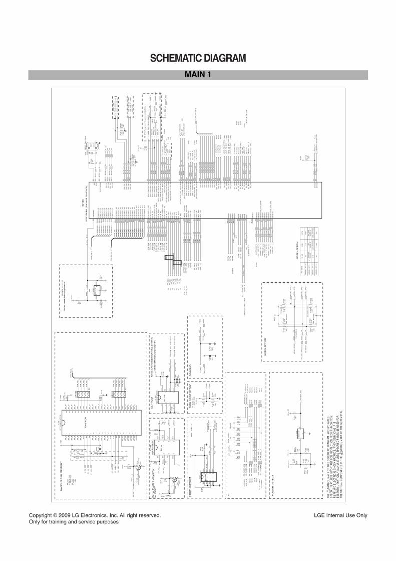
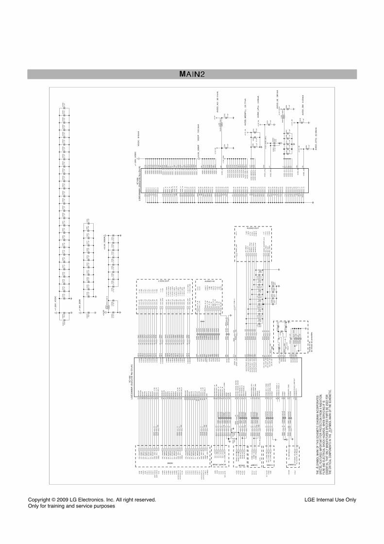
SCHEMATIC DIAGRAM
Copyright © 2009 LG Electronics. Inc. All right reserved. Only for training and service purposes
LGE Internal Use Only
MAIN 1
THE
S
YMBO
L M
ARK
OF
THIS
SCH
EMET
IC D
IAG
RAM
INCO
RPO
RATE
SSP
ECIA
L FE
ATUR
ES IM
PORT
ANT
FOR
PRO
TECT
ION
FRO
M X
-RAD
IATI
ON.
FILR
E AN
D EL
ECTR
ICAL
SHO
CK H
AZAR
DS, W
HEN
SERV
ICIN
G IF
IS
ESSE
NTIA
L TH
AT O
NLY
MAN
UFAT
URES
SPE
CFIE
D PA
RTS
BE U
SED
FOR
THE
CRIT
ICAL
CO
MPO
NENT
S IN
THE
SYM
BOL
MAR
K O
F TH
E SC
HEM
ETIC
.
SC
1_
CV
BS
_IN
E2
1;9
:O4
FE
_V
MA
IN1
0:A
A8
AV
_C
VB
S_
IN4
:M2
SC
1_
R_
IN9
:J1
2
SC
1_
FB
9:O
6
SC
1_
L_
IN9
:J1
0
SC
AR
T1
_R
ou
t9
:T1
4S
CA
RT
1_
Lo
ut
9:S
12
SP
DIF
_O
UT
4:T
11
HP
_R
OU
T7
:G2
1H
P_
LO
UT
7:G
19
SC
AR
T2
_L
ou
t9
:AM
13
SC
AR
T2
_R
ou
t9
:AN
15
DT
V/M
NT
_V
OU
T9
:AL
4
SC
1_
ID9
:P8
SC
1_
CV
BS
_IN
E1
7;9
:O4
SC
2_
CV
BS
_IN
9:A
E2
R2
28
10
0
R2
09
10
0
C2
30
2.2
uF
C2
29
2.2
uF
DS
UB
_H
SY
NC
4:C
22
DS
UB
_V
SY
NC
4:C
22
R2
29
39
0
1%
Ch
ec
k
FE
_S
IF1
0:P
13
R2
41
47
MS
_L
RC
K7
:F1
2
MS
_L
RC
H7
:F1
2
AU
DIO
_M
AS
TE
R_
CL
K7
:F7
MS
_S
CK
7:F
12
R2
31
22
R2
32
22
R2
33
22
R2
34
22
+3
.3V
R2
42
47
+3
.3V
_A
VD
D
+1
.8V
_D
DR
+3
.3V
_S
6
L2
09
BL
M1
8P
G1
21
SN
1D+3
.3V
+3
.3V
_S
6
L2
06
BL
M1
8P
G1
21
SN
1D
+3
.3V
_S
6
+3
.3V
_S
6
L2
10
BL
M1
8P
G1
21
SN
1D
+3
.3V
_V
DD
P+
3.3
V+1
.8V
_D
DR
C2
00
62
.2u
FC
20
07
2.2
uF
+3
.3V
_A
VD
D_
MP
LL
+1
.26
V_
VD
DC
+1
.26
V_
VD
DC
+3
.3V
_V
DD
P
R2
04
10
0
R2
10
47
R2
15
47
R2
16
47
R2
11
47
R2
13
47
R2
17
47
R2
12
47
R2
18
47
R2
06
47
R2
20
47
R2
24
47
R2
05
47
R2
19
47
R2
26
47
R2
23
47
R2
22
47
R2
27
47
R2
46
22
R2
45
22
C2
22
0.0
47
uF
C2
14
0.0
47
uF
C2
01
0.0
47
uF
C2
17
0.0
47
uF
C2
21
0.0
47
uF
C2
10
0.0
47
uF
C2
07
0.0
47
uF
C2
16
0.0
47
uF
C2
06
0.0
47
uF
C2
04
0.0
47
uF
C2
12
0.0
47
uF
C2
00
0.0
47
uF
C2
18
0.0
47
uF
C2
05
0.0
47
uF
C2
15
0.0
47
uF
C2
13
0.0
47
uF
C2
02
0.0
47
uF
C2
11
0.0
47
uF
C2
31
0.1
uF
C2
32
0.1
uF
C2
24
0.1
uF
C2
00
82
.2u
F
C2
00
92
.2u
FS
C2
_L
_IN
9:A
E1
0
SC
2_
R_
IN9
:AE
11
C2
01
12
.2u
F
C2
01
22
.2u
FC
20
13
2.2
uF
C2
01
42
.2u
F
C2
01
52
.2u
F
C2
01
62
.2u
F
C2
02
40
.04
7u
FR
23
54
7
C2
01
90
.04
7u
FR
23
64
7
R2
37
10
0
R2
38
10
0
R2
39
10
0
R2
40
10
0
R2
50
10
0
R2
51
10
0
R25222K
R25322K
R25422K
R25522K
R25622K
R25722K
C20180.01uF
C20210.01uF
C20230.01uF
C20170.01uF
C20220.01uF
C20200.01uF
C2
39
22
pF
OP
T
C2
36
22
pF
OP
T
C2
38
22
pF
OP
T
C2
37
22
pF
OP
T
R2
43
10
KR
24
41
0K
CK
-_H
DM
I16
:K8
DD
C_
SD
A_
16
:K7
;6:A
L9
D2
+_
HD
MI1
6:K
12
D1
+_
HD
MI1
6:K
11
D1
-_H
DM
I16
:K1
0
CK
+_
HD
MI1
6:K
9
D0
+_
HD
MI1
6:K
10
D0
-_H
DM
I16
:K9
DD
C_
SC
L_
16
:K7
;6:A
L9
HP
D1
6:J
6
D2
-_H
DM
I16
:K1
1
R2
00
10
0
D0
-_H
DM
I26
:K2
0
D2
-_H
DM
I26
:K2
2
CK
-_H
DM
I26
:K1
9
D0
+_
HD
MI2
6:K
21
HP
D2
6:J
16
D2
+_
HD
MI2
6:K
22
DD
C_
SC
L_
26
:K1
8;6
:AL
18
CK
+_
HD
MI2
6:K
20
D1
+_
HD
MI2
6:K
21
DD
C_
SD
A_
26
:K1
8;6
:AL
19
D1
-_H
DM
I26
:K2
1
D0
-_H
DM
I36
:X1
5
D2
-_H
DM
I36
:X1
7
CK
-_H
DM
I36
:X1
4
D0
+_
HD
MI3
6:X
15
HP
D3
6:W
11
D2
+_
HD
MI3
6:X
17
DD
C_
SC
L_
36
:X1
3;6
:AL
13
CK
+_
HD
MI3
6:X
15
D1
+_
HD
MI3
6:X
16
DD
C_
SD
A_
36
:X1
3;6
:AL
14
D1
-_H
DM
I36
:X1
6
HD
MI_
CE
C6
:AM
25
DS
UB
_R
4:C
26
DS
UB
_G
4:C
24
DS
UB
_B
4:C
23
CO
MP
_P
r4
:K1
3
CO
MP
_P
b4
:K1
2
CO
MP
_Y
4:K
11
SC
1_
R9
:J6
SC
1_
B9
:J9
SC
1_
G9
:J8
PC
_L
_IN
4:Z
6
PC
_R
_IN
4:Z
5
AV
_L
_IN
4:M
5
AV
_R
_IN
4:M
6
CO
MP
_L
_IN
4:K
13
CO
MP
_R
_IN
4:K
15
LV
A_
2M
11
:Q7
LV
B_
3M
11
:Q1
5;1
1:Q
9
LV
B_
2P
11
:J9
;11
:M1
5
LV
B_
0M
11
:Q1
6;1
1:Q
10
LV
A_
4M
11
:Q6
LV
B_
1M
11
:Q1
6;1
1:Q
10
LV
A_
CK
P1
1:J
7
LV
B_
0P
11
:J1
0;1
1:M
16
LV
A_
1M
11
:Q7
LV
A_
0P
11
:J8
LV
B_
3P
11
:J9
;11
:M1
5
LV
A_
4P
11
:J6
LV
A_
3P
11
:J7
LV
A_
CK
M1
1:Q
7
LV
B_
4M
11
:Q1
5;1
1:Q
9
LV
B_
1P
11
:J1
0;1
1:M
16
LV
B_
4P
11
:J9
;11
:M1
5
LV
A_
0M
11
:Q8
LV
B_
CK
P1
1:J
9;1
1:M
15
LV
A_
2P
11
:J7
LV
A_
3M
11
:Q7
LV
B_
CK
M1
1:Q
15
;11
:Q9
LV
A_
1P
11
:J7
LV
B_
2M
11
:Q1
5;1
1:Q
10
R2
58
22
R2
59
22
R2
61
22
R2
60
22
R2
64
22
R2
62
22
R2
63
22
R2
65
22
5V
_H
DM
I_3
R2
67
22
R2
68
22
R2
69
22
R2
70
22
R2
71
22
R2
72
22
R2
73
22
R2
75
22
R2
76
22
R2
77
22
R2
78
22
R2
79
22
R2
80
22
R2
81
22
R2
82
22
R2
83
22
R2
47
10
0
+3
.3V
_S
6
C2
25
10
uF
6.3
V
C2
04
41
0u
FC
20
43
10
uF
C2
02
51
0u
F6
.3V
R2
84
10
0S
C2
_ID
9:P
8
R2
14
47
0
R2
25
47
0
R2
21
47
0
R2
74
10
0
OP
T
C2
09
10
00
pF
C2
08
10
00
pF
C2
03
10
00
pF
FE
_V
SC
AR
T_
OU
T
R2
08
0
R2
01
0
R2
02
0
R2
48
0
R2
49
0
R2
07
0
C2
23
0.1
uF
C2
26
0.1
uF
C2
03
10
.1u
FC
24
60
.1u
F
C2
00
40
.1u
FC
20
26
0.1
uF
C2
47
0.1
uF
C2
52
0.1
uF
C2
03
40
.1u
FC
20
42
0.1
uF
C2
97
0.1
uF
C2
59
0.1
uF
C2
75
0.1
uF
C2
49
0.1
uF
C2
03
80
.1u
FC
26
40
.1u
FC
20
35
0.1
uF
C2
45
0.1
uF
C2
48
0.1
uF
C2
57
0.1
uF
C2
58
0.1
uF
C2
41
0.1
uF
C2
81
0.1
uF
C2
00
50
.1u
FC
20
03
0.1
uF
C2
96
0.1
uF
C2
04
10
.1u
F
C2
65
0.1
uF
C2
03
60
.1u
F
C2
51
0.1
uF
C2
00
10
.1u
FC
28
90
.1u
F
C2
53
0.1
uF
C2
03
90
.1u
F
C2
83
0.1
uF
C2
43
0.1
uF
C2
00
00
.1u
FC
29
40
.1u
F
C2
76
0.1
uF
C2
42
0.1
uF
C2
04
00
.1u
F
C2
77
0.1
uF
C2
54
0.1
uF
C2
91
0.1
uF
C2
03
20
.1u
FC
20
33
0.1
uF
C2
03
70
.1u
F
C2
66
0.1
uF
C2
50
0.1
uF
C2
44
0.1
uF
C2
03
0
0.1
uF
C2
62
0.1
uF
C2
93
0.1
uF
C2
02
90
.1u
F
C2
73
0.1
uF
C2
56
0.1
uF
C2
79
0.1
uF
C2
71
0.1
uF
C2
60
0.1
uF
C2
84
0.1
uF
C2
63
0.1
uF
C2
67
0.1
uF
C2
74
0.1
uFC
26
9
0.1
uF
C2
86
0.1
uF
C2
34
0.1
uF
C2
35
0.1
uF
C2
33
0.1
uF
R2
03
10
0
R2
30
10
0
R2
66
10
0
C2
27
1u
F
C2
02
71
0u
F
C2
28
4.7
uF
LG
E3
36
8A
(S
atu
rn6
No
-Div
X)
IC1
00
RX
AC
KP
F1
RX
AC
KN
F2
RX
A0
PG
2
RX
A0
NG
3
RX
A1
PH
3
RX
A1
NG
1
RX
A2
PH
1
RX
A2
NH
2
DD
CD
_A
_D
AA
1
DD
CD
_A
_C
KB
2
HO
TP
LU
G_
AA
2
RX
BC
KP
C3
RX
BC
KN
B1
RX
B0
PC
1
RX
B0
NC
2
RX
B1
PD
2
RX
B1
ND
3
RX
B2
PE
3
RX
B2
ND
1
DD
CD
_B
_D
AE
1
DD
CD
_B
_C
KF
3
HO
TP
LU
G_
BE
2
RX
CC
KP
AE
8
RX
CC
KN
AD
8
RX
C0
PA
D9
RX
C0
NA
F8
RX
C1
PA
F9
RX
C1
NA
E9
RX
C2
PA
E1
0
RX
C2
NA
D1
0
DD
CD
_C
_D
AA
E7
DD
CD
_C
_C
KA
F7
HO
TP
LU
G_
CA
D7
CE
CJ
3
HS
YN
C0
/SC
1_
IDN
2
VS
YN
C0
/SC
1_
FB
N1
RIN
0P
/SC
1_
RP
2
GIN
0P
/SC
1_
GR
3
BIN
0P
/SC
1_
BR
1
SO
GIN
0/S
C1
_C
VB
SP
3
RIN
MP
1
BIN
MT
3
GIN
MR
2
HS
YN
C1
/DS
UB
_H
SY
NC
K3
VS
YN
C1
/DS
UB
_V
SY
NC
K2
RIN
1P
/DS
UB
_R
L1
GIN
1P
/DS
UB
_G
L3
BIN
1P
/DS
UB
_B
K1
SO
GIN
1L
2
RIN
2P
/CO
MP
_P
R+
V1
GIN
2P
/CO
MP
_Y
+V
2
BIN
2P
/CO
MP
_P
B+
U1
SO
GIN
2V
3
VS
YN
C2
J5
CV
BS
1/S
C1
_C
VB
SU
3
CV
BS
2/S
C2
_C
VB
SU
2
CV
BS
3/S
IDE
_C
VB
ST
1
VC
OM
1T
2
CV
BS
4/S
-VID
EO
_Y
M1
CV
BS
6/S
-VID
EO
_C
M2
CV
BS
5N
3
CV
BS
7M
3
CV
BS
0/R
F_
CV
BS
W1
VC
OM
0Y
3
CV
BS
OU
T0
/SC
2_
MN
TO
UT
Y2
CV
BS
OU
T1
AA
2
LV
A0
PA
E1
6
LV
A0
MA
D1
6
LV
A1
PA
D1
5
LV
A1
MA
F1
6
LV
A2
PA
F1
5
LV
A2
MA
E1
5
LV
A3
PA
D1
3
LV
A3
MA
F1
4
LV
A4
PA
F1
3
LV
A4
MA
E1
3
LV
AC
KP
AE
14
LV
AC
KM
AD
14
LV
B0
PA
E2
0
LV
B0
MA
D2
0
LV
B1
PA
D1
9
LV
B1
MA
F2
0
LV
B2
PA
F1
9
LV
B2
MA
E1
9
LV
B3
PA
D1
7
LV
B3
MA
F1
8
LV
B4
PA
F1
7
LV
B4
MA
E1
7
LV
BC
KP
AE
18
LV
BC
KM
AD
18
AU
R0
AA
3
AU
L0
Y1
AU
R1
AE
1
AU
L1
AF
3
AU
R2
AE
3
AU
L2
AE
2
AU
R3
AA
1
AU
L3
AB
1
AU
R4
AB
2
AU
L4
AC
2
AU
R5
AB
3
AU
L5
AC
3
SIF
0P
W3
SIF
0M
W2
SP
DIF
_IN
F1
1
SP
DIF
_O
UT
E9
AU
OU
TR
0/H
P_
RO
UT
AF
1
AU
OU
TL
0/H
P_
LO
UT
AF
2
AU
OU
TR
1/S
C1
_R
OU
TA
D3
AU
OU
TL
1/S
C1
_L
OU
TA
D1
AU
OU
TR
2/S
C2
_R
OU
TA
C1
AU
OU
TL
2/S
C2
_L
OU
TA
D2
I2S
_O
UT
_M
CK
A8
I2S
_O
UT
_W
SB
7
I2S
_O
UT
_B
CK
C7
I2S
_O
UT
_S
DD
8
I2S
_IN
_S
DC
8
VC
LA
MP
K4
RE
FP
H4
RE
FM
J4
RE
XT
G4
AU
CO
MA
E5
AU
VR
MA
E4
AU
VR
PA
F4
AU
VA
GA
D4
IC1
00
LG
E3
36
8A
(S
atu
rn6
No
-Div
X)
VD
DC
_1
D1
6
VD
DC
_2
D1
7
VD
DC
_3
D1
8
VD
DC
_4
D1
9
VD
DC
_5
D2
0
VD
DC
_6
H1
8
VD
DC
_7
H1
9
VD
DC
_8
H2
0
VD
DC
_9
J2
0
VD
DC
_1
0K
20
VD
DC
_1
1L
20
VD
DC
_1
2M
20
VD
DC
_1
3P
7
VD
DC
_1
4R
7
VD
DC
_1
5T
7
VD
DC
_1
6T
22
VD
DC
_1
7U
7
VD
DC
_1
8U
20
VD
DC
_1
9U
22
VD
DC
_2
0V
7
VD
DC
_2
1V
22
VD
DC
_2
2W
11
VD
DC
_2
3W
12
VD
DC
_2
4W
19
VD
DC
_2
5W
20
VD
DC
_2
6W
22
VD
DC
_2
7Y
22
VD
DP
_1
H9
VD
DP
_2
H1
0
VD
DP
_3
H1
1
VD
DP
_4
H1
2
VD
DP
_5
N2
0
VD
DP
_6
P2
0
VD
DP
_7
W9
VD
DP
_8
W1
0
AV
DD
_A
UW
7
AV
DD
_D
DR
_1
G1
2
AV
DD
_D
DR
_2
G1
3
AV
DD
_D
DR
_3
H1
3
AV
DD
_D
DR
_4
H1
4
AV
DD
_D
DR
_5
H1
5
AV
DD
_D
DR
_6
H1
6
AV
DD
_D
DR
_7
W1
4
AV
DD
_D
DR
_8
W1
5
AV
DD
_D
DR
_9
W1
6
AV
DD
_D
DR
_1
0W
17
AV
DD
_D
DR
_1
1W
18
AV
DD
_M
EM
PL
L_
1H
17
AV
DD
_M
EM
PL
L_
2T
20
AV
DD
_M
EM
PL
L_
3V
20
AV
DD
_L
PL
LR
20
AV
DD
_M
PL
LH
7
AV
DD
_3
3_
1J
7
AV
DD
_3
3_
2K
7
AV
DD
_3
3_
3L
7
AV
DD
_3
3_
4M
7
AV
DD
_3
3_
5N
7
AV
DD
_D
MW
8
AV
DD
_U
SB
H8
GN
D_
2E
16
GN
D_
3E
17
GN
D_
4E
18
GN
D_
5F
7
GN
D_
6L
9
GN
D_
7L
10
GN
D_
8L
11
GN
D_
9L
12
GN
D_
10
L1
3
GN
D_
11
L1
4
GN
D_
12
L1
5
GN
D_
13
L1
6
GN
D_
14
L1
7
GN
D_
15
L1
8
GN
D_
16
M9
GN
D_
17
M1
0
GN
D_
18
M1
1
GN
D_
19
M1
2
GN
D_
20
M1
3
GN
D_
21
M1
4
GN
D_
22
M1
5
GN
D_
23
M1
6
GN
D_
24
M1
7
GN
D_
25
M1
8
GN
D_
26
N4
GN
D_
27
N9
GN
D_
28
N1
0
GN
D_
29
N1
1
GN
D_
30
N1
2
GN
D_
31
N1
3
GN
D_
32
N1
4
GN
D_
33
N1
5
GN
D_
34
N1
6
GN
D_
35
N1
7
GN
D_
36
N1
8
GN
D_
37
P4
GN
D_
38
P9
GN
D_
39
P1
0
GN
D_
40
P1
1
GN
D_
41
P1
2
GN
D_
42
P1
3
GN
D_
43
P1
4
GN
D_
44
P1
5
GN
D_
45
P1
6
GN
D_
46
P1
7
GN
D_
47
P1
8
GN
D_
48
R4
GN
D_
49
R9
GN
D_
50
R1
0
GN
D_
51
R1
1
GN
D_
52
R1
2
GN
D_
53
R1
3
GN
D_
54
R1
4
GN
D_
55
R1
5
GN
D_
56
R1
6
GN
D_
57
R1
7
GN
D_
58
R1
8
GN
D_
59
T5
GN
D_
60
T9
GN
D_
61
T1
0
GN
D_
62
T1
1
GN
D_
63
T1
2
GN
D_
64
T1
3
GN
D_
65
T1
4
GN
D_
66
T1
5
GN
D_
67
T1
6
GN
D_
68
T1
7
GN
D_
69
T1
8
GN
D_
70
U5
GN
D_
71
W1
3
GN
D_
72
Y2
1
GN
D_
73
AA
23
Clo
se
to
IC
as c
lose
as p
ossib
le
HDMISCART_RGB DSUB CVBS TV/MNTCOMP
AUDIO INLVDS OUT
AUDIO OUT
VD
DC
: 9
70
mA
VD
DP
: 1
02
.3m
A
AV
DD
_A
U :
36
.11
mA
AV
DD
_M
EM
PL
L :
23
.77
mA
AV
DD
_L
PL
L :
4.6
9m
A
AV
DD
_3
3 :
28
1m
A
AV
DD
_D
M :
0.0
3m
A
AV
DD
_O
TG
: 2
2.9
6m
A
Copyright © 2009 LG Electronics. Inc. All right reserved. Only for training and service purposes
LGE Internal Use Only
M
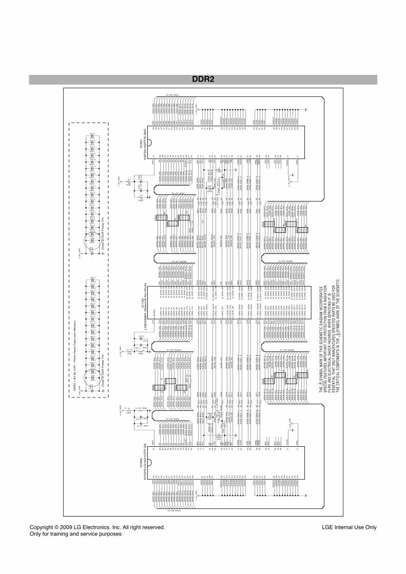
SD
DR
_A
[12
]
SD
DR
_A
[11
]
SD
DR
_A
[10
]
SD
DR
_A
[9]
SD
DR
_A
[0]
SD
DR
_A
[1]
SD
DR
_A
[2]
SD
DR
_A
[3]
SD
DR
_A
[4]
SD
DR
_A
[5]
SD
DR
_A
[6]
SD
DR
_A
[7]
SD
DR
_A
[8]
SD
DR
_A
[1]
SD
DR
_A
[10
]
SD
DR
_A
[12
]
SD
DR
_A
[7]
SD
DR
_A
[0]
SD
DR
_A
[2]
SD
DR
_A
[4]
SD
DR
_A
[6]
SD
DR
_A
[11
]
SD
DR
_A
[8]
TD
DR
_A
[4]
TD
DR
_A
[11
]
TD
DR
_A
[3]
TD
DR
_A
[10
]
TD
DR
_A
[12
]
TD
DR
_A
[2]
TD
DR
_A
[5]
TD
DR
_A
[8]
TD
DR
_A
[1]
TDDR_A[0-12]
TD
DR
_A
[1]
TD
DR
_A
[4]
TD
DR
_A
[3]
TD
DR
_A
[11
]
TD
DR
_A
[5]
TD
DR
_A
[12
]T
DD
R_
A[6
]
TD
DR
_A
[2]
TD
DR
_A
[10
]
TD
DR
_A
[0]
TD
DR
_A
[8]
TD
DR
_A
[9]
TD
DR
_A
[7]
TD
DR
_A
[0]
TD
DR
_A
[6]
TD
DR
_A
[9]
SD
DR
_D
[10
]
SD
DR
_D
[11
]
SD
DR
_D
[12
]
SD
DR
_D
[10
]
SD
DR
_D
[8]
SD
DR
_D
[3]
SD
DR
_D
[8]
SD
DR
_D
[1]
SD
DR
_D
[9]
SD
DR
_D
[4]
SD
DR
_D
[3]
SD
DR
_D
[5]
SD
DR
_D
[1]
SD
DR
_D
[6]
SD
DR
_D
[2]
SD
DR
_D
[4]
SD
DR
_D
[14
]
SD
DR
_D
[15
]
SD
DR
_D
[6]
SD
DR
_D
[9]
SD
DR
_D
[7]
SD
DR
_D
[0]
SD
DR
_D
[13
]
SD
DR
_D
[5]
SD
DR
_D
[2]
SD
DR
_D
[0]
SD
DR
_D
[12
]
SD
DR
_D
[13
]
SD
DR
_D
[14
]
SD
DR
_D
[15
]
SD
DR
_D
[7]
SD
DR
_D
[11
]
TD
DR
_D
[2]
TD
DR
_D
[6]
TD
DR
_D
[1]
TD
DR
_D
[5]
TD
DR
_D
[11
]
TD
DR
_D
[3]
TD
DR
_D
[7]
TD
DR
_D
[4]
TD
DR
_D
[9]
TD
DR
_D
[1]
TD
DR
_D
[8]
TD
DR
_D
[3]
TD
DR
_D
[8]
TD
DR
_D
[10
]
TD
DR
_D
[12
]
TD
DR
_D
[11
]
TD
DR
_D
[15
]
TD
DR
_D
[10
]
TD
DR
_D
[14
]
TD
DR
_D
[13
]
TD
DR
_D
[12
]
TD
DR
_D
[0]
TD
DR
_D
[2]
TD
DR
_D
[5]
TD
DR
_D
[13
]
TD
DR
_D
[0]
TD
DR
_D
[7]
TD
DR
_D
[9]
TD
DR
_D
[6]
TD
DR
_D
[15
]
TD
DR
_D
[14
]
TD
DR
_D
[4]
SD
DR
_B
A[0
]
SD
DR
_B
A[1
]
AD
DR
2_
BA
[2]
/AD
DR
2_
MC
LK
SD
DR
_C
KE
AD
DR
2_
CK
E
/SD
DR
_C
K
SD
DR
_C
K
/SD
DR
_R
AS
/SD
DR
_C
AS
/SD
DR
_W
E
SD
DR
_D
QS
1_
P
SD
DR
_D
QS
0_
P
SD
DR
_D
QM
1_
P
SD
DR
_D
QM
0_
P
SD
DR
_D
QS
1_
N
SD
DR
_D
QS
0_
N
/AD
DR
2_
RA
S
AD
DR
2_
OD
T
/AD
DR
2_
CA
S
/AD
DR
2_
WE
AD
DR
2_
DQ
S1
_P
AD
DR
2_
DQ
S0
_P
AD
DR
2_
DQ
M1
_P
AD
DR
2_
DQ
M0
_P
AD
DR
2_
DQ
S0
_N
AD
DR
2_
DQ
S1
_N
BD
DR
2_
DQ
M0
_P
BD
DR
2_
DQ
S1
_P
BD
DR
2_
OD
T
BD
DR
2_
DQ
S0
_N
TD
DR
_C
KE
TD
DR
_M
CL
K
BD
DR
2_
DQ
S0
_P
BD
DR
2_
MC
LK
/TD
DR
_M
CL
K
TD
DR
_D
QM
1_
P
BD
DR
2_
DQ
S1
_N
BD
DR
2_
DQ
M1
_P
/TD
DR
_C
AS
BD
DR
2_
BA
[2]
TD
DR
_B
A[1
]
/TD
DR
_W
E
TD
DR
_D
QS
1_
P
TD
DR
_B
A[0
]
TD
DR
_D
QS
1_
N
TD
DR
_D
QS
0_
P
BD
DR
2_
BA
[0]
/TD
DR
_R
AS
BD
DR
2_
BA
[1]
TD
DR
_D
QM
0_
P
/BD
DR
2_
MC
LK
TD
DR
_D
QS
0_
N
SD
DR
_A
[3]
SDDR_A[0-12]
ADDR2_A[0-12]
AD
DR
2_
A[0
]
AD
DR
2_
A[1
]
AD
DR
2_
A[3
]
AD
DR
2_
A[2
]
AD
DR
2_
A[5
]
AD
DR
2_
A[7
]
AD
DR
2_
A[6
]
AD
DR
2_
A[4
]
AD
DR
2_
A[9
]
AD
DR
2_
A[8
]
AD
DR
2_
A[1
0]
AD
DR
2_
A[1
1]
AD
DR
2_
A[1
2]
AD
DR
2_
A[3
]
AD
DR
2_
A[1
]
AD
DR
2_
A[1
0]
AD
DR
2_
A[9
]
AD
DR
2_
A[1
2]
AD
DR
2_
A[7
]
AD
DR
2_
A[0
]
AD
DR
2_
A[2
]
AD
DR
2_
A[4
]
AD
DR
2_
A[6
]
AD
DR
2_
A[1
1]
AD
DR
2_
A[8
]
AD
DR
2_
BA
[0]
AD
DR
2_
BA
[1]
AD
DR
2_
MC
LK
BDDR2_A[0-12]
BD
DR
2_
A[0
]
BD
DR
2_
A[1
]
BD
DR
2_
A[2
]
BD
DR
2_
A[3
]
BD
DR
2_
A[4
]
BD
DR
2_
A[5
]
BD
DR
2_
A[6
]
BD
DR
2_
A[7
]
BD
DR
2_
A[8
]
BD
DR
2_
A[9
]
BD
DR
2_
A[1
0]
BD
DR
2_
A[1
1]
BD
DR
2_
A[1
2]
BD
DR
2_
A[9
]
BD
DR
2_
A[3
]
BD
DR
2_
A[1
]
BD
DR
2_
A[1
0]
BD
DR
2_
A[5
]
BD
DR
2_
A[1
2]
BD
DR
2_
A[0
]
BD
DR
2_
A[2
]
BD
DR
2_
A[4
]
BD
DR
2_
A[6
]
BD
DR
2_
A[1
1]
BD
DR
2_
A[8
]
BD
DR
2_
CK
E
/BD
DR
2_
RA
S
/BD
DR
2_
CA
S
/BD
DR
2_
WE
ADDR2_D[0-15]
AD
DR
2_
D[0
]
AD
DR
2_
D[1
]
AD
DR
2_
D[3
]
AD
DR
2_
D[2
]
AD
DR
2_
D[5
]
AD
DR
2_
D[4
]
AD
DR
2_
D[6
]
AD
DR
2_
D[7
]
AD
DR
2_
D[1
2]
AD
DR
2_
D[9
]
AD
DR
2_
D[8
]
AD
DR
2_
D[1
4]
AD
DR
2_
D[1
0]
AD
DR
2_
D[1
5]
AD
DR
2_
D[1
1]
AD
DR
2_
D[1
3]
AD
DR
2_
D[1
1]
AD
DR
2_
D[1
2]
AD
DR
2_
D[4
]
AD
DR
2_
D[3
]
AD
DR
2_
D[1
]
AD
DR
2_
D[6
]
AD
DR
2_
D[9
]
AD
DR
2_
D[1
4]
AD
DR
2_
D[1
5]
AD
DR
2_
D[1
3]
AD
DR
2_
D[1
0]
AD
DR
2_
D[8
]
AD
DR
2_
D[5
]
AD
DR
2_
D[7
]
AD
DR
2_
D[2
]
AD
DR
2_
D[0
]
SDDR_D[0-15]
BDDR2_D[0-15]
BD
DR
2_
D[0
]
BD
DR
2_
D[1
]
BD
DR
2_
D[2
]
BD
DR
2_
D[3
]
BD
DR
2_
D[6
]
BD
DR
2_
D[4
]
BD
DR
2_
D[7
]
BD
DR
2_
D[5
]
BD
DR
2_
D[1
0]
BD
DR
2_
D[8
]
BD
DR
2_
D[1
2]
BD
DR
2_
D[1
4]
BD
DR
2_
D[1
5]
BD
DR
2_
D[1
1]
BD
DR
2_
D[9
]
BD
DR
2_
D[1
3]
BD
DR
2_
D[1
1]
BD
DR
2_
D[1
2]
BD
DR
2_
D[1
4]
BD
DR
2_
D[9
]
BD
DR
2_
D[1
3]
BD
DR
2_
D[1
0]
BD
DR
2_
D[8
]
BD
DR
2_
D[1
5]
BD
DR
2_
D[4
]
BD
DR
2_
D[3
]
BD
DR
2_
D[1
]
BD
DR
2_
D[6
]
BD
DR
2_
D[7
]
BD
DR
2_
D[5
]
BD
DR
2_
D[0
]
BD
DR
2_
D[2
]
TDDR_D[0-15]
SD
DR
_A
[9]
SD
DR
_A
[5]
AD
DR
2_
A[5
]
BD
DR
2_
A[7
]T
DD
R_
A[7
]
SD
DR
_O
DT
TD
DR
_B
A[2
]S
DD
R_
BA
[2]
+1
.8V
_D
DR
+1
.8V
_D
DR
+1
.8V
_D
DR
+1
.8V
_D
DR
+1
.8V
_D
DR
+1
.8V
_D
DR
+1
.8V
_D
DR
AR
30
0
56
AR
30
1
56
AR
30
2
56
AR
30
3
56
AR
30
5
56
AR
30
4
56
AR
30
6
56
AR
30
8
56
AR
30
7 56
AR
30
9 56
AR
31
0
56
AR
31
2 56
AR
31
1
56
AR
31
3
56
R3
06
22
R3
07
22
R300150
OPT
R344150
OPT
R3
31
22
R3
30
22
+1
.8V
_D
DR
+1
.8V
_D
DR
+1
.8V
_D
DR
+1
.8V
_D
DR
C324
10uF
C303
10uF
IC3
01
H5
PS
51
62
FF
R-S
6C
J2
VR
EF
J8
CK
H2
VS
SQ
2
B7
UD
QS
N8
A4
P8
A8
L1
NC
4
L2
BA
0
R8
NC
3
K7
RA
S
F8
VS
SQ
3
F3
LD
M
P3
A9
M3
A1
N3
A5
K8
CK
R3
NC
5
L3
BA
1
J7
VS
SD
L
L7
CA
S
F2
VS
SQ
4
B3
UD
M
M2
A1
0/A
P
K2
CK
E
R7
NC
6
M7
A2
N7
A6
M8
A0
J1
VD
DL
K3
WE
E8
LD
QS
P7
A1
1
K9
OD
T
A2
NC
1
N2
A3
P2
A7
H8
VS
SQ
1
F7
LD
QS
A8
UD
QS
R2
A1
2
L8
CS
E2
NC
2
E7
VS
SQ
5D
8V
SS
Q6
D2
VS
SQ
7A
7V
SS
Q8
B8
VS
SQ
9B
2V
SS
Q1
0
P9
VS
S1
N1
VS
S2
J3
VS
S3
E3
VS
S4
A3
VS
S5
G9
VD
DQ
1G
7V
DD
Q2
G3
VD
DQ
3G
1V
DD
Q4
E9
VD
DQ
5C
9V
DD
Q6
C7
VD
DQ
7C
3V
DD
Q8
C1
VD
DQ
9A
9V
DD
Q1
0
R1
VD
D1
M9
VD
D2
J9
VD
D3
E1
VD
D4
A1
VD
D5
B9
DQ
15
B1
DQ
14
D9
DQ
13
D1
DQ
12
D3
DQ
11
D7
DQ
10
C2
DQ
9C
8D
Q8
F9
DQ
7F
1D
Q6
H9
DQ
5H
1D
Q4
H3
DQ
3H
7D
Q2
G2
DQ
1G
8D
Q0
IC3
00
HY
5P
S1
G1
63
1C
FP
-S6
J2
VR
EF
J8
CK
H2
VS
SQ
2
B7
UD
QS
N8
A4
P8
A8
L1
BA
2
L2
BA
0
R8
NC
3
K7
RA
S
F8
VS
SQ
3
F3
LD
M
P3
A9
M3
A1
N3
A5
K8
CK
R3
NC
5
L3
BA
1
J7
VS
SD
L
L7
CA
S
F2
VS
SQ
4
B3
UD
M
M2
A1
0/A
P
K2
CK
E
R7
NC
6
M7
A2
N7
A6
M8
A0
J1
VD
DL
K3
WE
E8
LD
QS
P7
A1
1
K9
OD
T
A2
NC
1
N2
A3
P2
A7
H8
VS
SQ
1
F7
LD
QS
A8
UD
QS
R2
A1
2
L8
CS
E2
NC
2
E7
VS
SQ
5D
8V
SS
Q6
D2
VS
SQ
7A
7V
SS
Q8
B8
VS
SQ
9B
2V
SS
Q1
0
P9
VS
S1
N1
VS
S2
J3
VS
S3
E3
VS
S4
A3
VS
S5
G9
VD
DQ
1G
7V
DD
Q2
G3
VD
DQ
3G
1V
DD
Q4
E9
VD
DQ
5C
9V
DD
Q6
C7
VD
DQ
7C
3V
DD
Q8
C1
VD
DQ
9A
9V
DD
Q1
0
R1
VD
D1
M9
VD
D2
J9
VD
D3
E1
VD
D4
A1
VD
D5
B9
DQ
15
B1
DQ
14
D9
DQ
13
D1
DQ
12
D3
DQ
11
D7
DQ
10
C2
DQ
9C
8D
Q8
F9
DQ
7F
1D
Q6
H9
DQ
5H
1D
Q4
H3
DQ
3H
7D
Q2
G2
DQ
1G
8D
Q0
R351
0
R350
0
OPT
C306
0.1uF
C337
0.1uF
C320
0.1uF
C326
0.1uF
C340
0.1uF
C338
0.1uF
C331
0.1uF
C329
0.1uF
C334
0.1uFC336
0.1uF
C341
0.1uF
C327
0.1uF
C319
0.1uF
C310
0.1uF
C342
0.1uF
C316
0.1uF
C3
23
0.1
uF
C330
0.1uF
C305
0.1uF
C317
0.1uF
C332
0.1uF
C314
0.1uF
C3
02
0.1
uF
C339
0.1uF
C308
0.1uF
C318
0.1uF
C307
0.1uF
C304
0.1uF
C328
0.1uF
C315
0.1uF
C313
0.1uF
C312
0.1uF
C325
0.1uF
C3
33
0.1
uF
C3010.1uF
C3000.1uF
C3
35
0.1
uF
C311
0.1uF
C3090.1uF
R3451K
1%
R3431K
1%
R321
1K1%
R322
1K1%
R301
1K1% R3021K1%
R3
48
4.7
KO
PT
R3
47
4.7
KO
PT
R3
46
4.7
KO
PT
R3
49
4.7
KO
PT
R3
36
56
R3
20
56
R3
19
56
R3
17
56
R3
15
56
R3
10
56
R3
34
56
R3
13
56
R3
33
56
R3
18
56
R3
27
56
R3
08
56
R3
09
56
R3
39
56
R3
11
56
R3
40
56
R3
12
56
R3
32
56
R3
29
56
OP
TR
30
55
6
R3
03
56
R3
41
56
R3
14
56
R3
38
56
R3
04
56
R3
25
56
R3
37
56
R3
35
56
R3
26
56
R3
42
56
R3
28
56
R3
16
56
IC1
00
LG
E3
36
8A
(S
atu
rn6
No
-Div
X)
B_
DD
R2
_A
0T
26
B_
DD
R2
_A
1A
F2
6
B_
DD
R2
_A
2T
25
B_
DD
R2
_A
3A
F2
3
B_
DD
R2
_A
4T
24
B_
DD
R2
_A
5A
E2
3
B_
DD
R2
_A
6R
26
B_
DD
R2
_A
7A
D2
2
B_
DD
R2
_A
8R
25
B_
DD
R2
_A
9A
C2
2
B_
DD
R2
_A
10
AD
23
B_
DD
R2
_A
11
R2
4
B_
DD
R2
_A
12
AE
22
B_
DD
R2
_B
A0
AC
23
B_
DD
R2
_B
A1
AC
24
B_
DD
R2
_B
A2
AB
22
B_
DD
R2
_M
CL
KV
25
/B_
DD
R2
_M
CL
KV
24
B_
DD
R2
_C
KE
AB
23
B_
DD
R2
_O
DT
U2
6
/B_
DD
R2
_R
AS
U2
5
/B_
DD
R2
_C
AS
U2
4
/B_
DD
R2
_W
EA
B2
4
B_
DD
R2
_D
QS
0A
B2
6
B_
DD
R2
_D
QS
1A
A2
6
B_
DD
R2
_D
QM
0A
C2
5
B_
DD
R2
_D
QM
1A
C2
6
B_
DD
R2
_D
QS
B0
AB
25
B_
DD
R2
_D
QS
B1
AA
25
B_
DD
R2
_D
Q0
W2
5
B_
DD
R2
_D
Q1
AE
26
B_
DD
R2
_D
Q2
W2
4
B_
DD
R2
_D
Q3
AF
24
B_
DD
R2
_D
Q4
AF
25
B_
DD
R2
_D
Q5
V2
6
B_
DD
R2
_D
Q6
AE
25
B_
DD
R2
_D
Q7
W2
6
B_
DD
R2
_D
Q8
Y2
6
B_
DD
R2
_D
Q9
AD
25
B_
DD
R2
_D
Q1
0Y
25
B_
DD
R2
_D
Q1
1A
E2
4
B_
DD
R2
_D
Q1
2A
D2
6
B_
DD
R2
_D
Q1
3Y
24
B_
DD
R2
_D
Q1
4A
D2
4
B_
DD
R2
_D
Q1
5A
A2
4
A_
MV
RE
FD
15
A_
DD
R2
_A
0C
13
A_
DD
R2
_A
1A
22
A_
DD
R2
_A
2B
13
A_
DD
R2
_A
3C
22
A_
DD
R2
_A
4A
13
A_
DD
R2
_A
5A
23
A_
DD
R2
_A
6C
12
A_
DD
R2
_A
7B
23
A_
DD
R2
_A
8B
12
A_
DD
R2
_A
9C
23
A_
DD
R2
_A
10
B2
2
A_
DD
R2
_A
11
A1
2
A_
DD
R2
_A
12
A2
4
A_
DD
R2
_B
A0
C2
4
A_
DD
R2
_B
A1
B2
4
A_
DD
R2
_B
A2
D2
4
A_
DD
R2
_M
CL
KB
14
/A_
DD
R2
_M
CL
KA
14
A_
DD
R2
_C
KE
D2
3
A_
DD
R2
_O
DT
D1
4
/A_
DD
R2
_R
AS
D1
3
/A_
DD
R2
_C
AS
D1
2
/A_
DD
R2
_W
ED
22
A_
DD
R2
_D
QS
0B
18
A_
DD
R2
_D
QS
1C
17
A_
DD
R2
_D
QM
0C
18
A_
DD
R2
_D
QM
1A
19
A_
DD
R2
_D
QS
B0
A1
8
A_
DD
R2
_D
QS
B1
B1
7
A_
DD
R2
_D
Q0
B1
5
A_
DD
R2
_D
Q1
A2
1
A_
DD
R2
_D
Q2
A1
5
A_
DD
R2
_D
Q3
B2
1
A_
DD
R2
_D
Q4
C2
1
A_
DD
R2
_D
Q5
C1
4
A_
DD
R2
_D
Q6
C2
0
A_
DD
R2
_D
Q7
C1
5
A_
DD
R2
_D
Q8
C1
6
A_
DD
R2
_D
Q9
C1
9
A_
DD
R2
_D
Q1
0B
16
A_
DD
R2
_D
Q1
1B
20
A_
DD
R2
_D
Q1
2A
20
A_
DD
R2
_D
Q1
3A
16
A_
DD
R2
_D
Q1
4B
19
A_
DD
R2
_D
Q1
5A
17
DD
R2
1.8
V B
y C
AP
- P
lace
th
ese
Ca
ps n
ea
r M
em
ory
Clo
se
to
DD
R P
ow
er
Pin
Clo
se
to
DD
R P
ow
er
Pin
THE
S
YMBO
L M
ARK
OF
THIS
SCH
EMET
IC D
IAG
RAM
INCO
RPO
RATE
SSP
ECIA
L FE
ATUR
ES IM
PORT
ANT
FOR
PRO
TECT
ION
FRO
M X
-RAD
IATI
ON.
FILR
E AN
D EL
ECTR
ICAL
SHO
CK H
AZAR
DS, W
HEN
SERV
ICIN
G IF
IS
ESSE
NTIA
L TH
AT O
NLY
MAN
UFAT
URES
SPE
CFIE
D PA
RTS
BE U
SED
FOR
THE
CRIT
ICAL
CO
MPO
NENT
S IN
THE
SYM
BOL
MAR
K O
F TH
E SC
HEM
ETIC
.
Copyright © 2009 LG Electronics. Inc. All right reserved. Only for training and service purposes
LGE Internal Use Only
DDR2
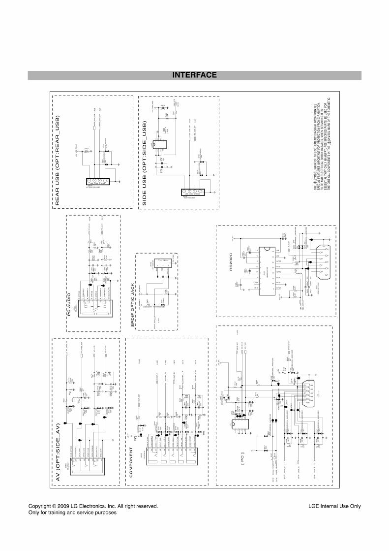
Fi ber Opt i c
USB DOWN STREAM
USB DOWN STREAM
THE
S
YMBO
L M
ARK
OF
THIS
SCH
EMET
IC D
IAG
RAM
INCO
RPO
RATE
SSP
ECIA
L FE
ATUR
ES IM
PORT
ANT
FOR
PRO
TECT
ION
FRO
M X
-RAD
IATI
ON.
FILR
E AN
D EL
ECTR
ICAL
SHO
CK H
AZAR
DS, W
HEN
SERV
ICIN
G IF
IS
ESSE
NTIA
L TH
AT O
NLY
MAN
UFAT
URES
SPE
CFIE
D PA
RTS
BE U
SED
FOR
THE
CRIT
ICAL
CO
MPO
NENT
S IN
THE
SYM
BOL
MAR
K O
F TH
E SC
HEM
ETIC
.
JP
41
2
DS
UB
_B
2:E
19
ISP
_R
XD
JP
41
4
P4
01
KC
N-D
S-1
-00
88
1
2
3
4
5
6
7
8
9
10
PC
_L
_IN
2:S
16
IC4
03
MA
X3
23
2C
DR
3C1-
2V+
4C2+
1C1+
6V-
5C2-
7DOUT2
8RIN2
9ROUT2
10DIN2
11DIN1
12ROUT1
13RIN1
14DOUT1
15GND
16VCC
P4
00
KC
N-D
S-1
-00
89
1
2
3
4
5
6
7
8
9
10
11
12
13
14
15
16
DS
UB
_G
2:E
19
CO
MP
_R
_IN
2:S
16
DS
UB
_R
2:E
18
CO
MP
_P
r2
:E2
0
DB
G_
TX
CO
MP
_D
ET
1:A
A2
2
DB
G_
RX
ISP
_T
XD
+5
V_
ST
+5
V_
ST
JP
41
3
CO
MP
_Y
2:E
20
+3
.3V
JK
40
1P
EJ
02
4-0
1
6B
T_
TE
RM
INA
L2
8S
HIE
LD
_P
LA
TE
7B
B_
TE
RM
INA
L2
5T
_S
PR
ING
4R
_S
PR
ING
7A
B_
TE
RM
INA
L1
6A
T_
TE
RM
INA
L1
3E
_S
PR
ING
CO
MP
_L
_IN
2:S
16
PC
_R
_IN
2:S
16
DS
UB
_H
SY
NC
2:E
18
DS
UB
_V
SY
NC
2:E
18
DS
UB
_D
ET
CO
MP
_P
b2
:E2
0
AV
_C
VB
S_
DE
T
+3
.3V
AV
_C
VB
S_
IN
AV
_R
_IN
AV
_L
_IN
+3
.3V
RE
AR
_U
SB
_D
P1
:AL
7
RE
AR
_U
SB
_D
M1
:AL
8
+5
V_
US
B_
RE
AR
C423
0.1uF
ED
ID_
WP
1:A
J1
9
R4
12
10
KR
41
61
00
D4
00
EN
KM
C2
83
8-T
11
2A
1
C
A2
+5
V_
ST
C4
02
18
pF
50
V
C4
01
18
pF
50
V
JK
40
2
PP
J2
18
-01
5C
[RD
]CO
NT
AC
T
2C
[RD
]U_
CA
N
4C
[RD
]O_
SP
RIN
G
2B
[WH
]U_
CA
N
3B
[WH
]C_
LU
G
2A
[YL
]U_
CA
N
5A
[YL
]CO
NT
AC
T
4A
[YL
]O_
SP
RIN
G
+5
V_
GE
NE
RA
L+
5V
_G
EN
ER
AL
JK
40
3
JS
T1
22
3-0
01
1
GN
D
2
VC
C
3
VIN
PU
T
4 FIX
_P
OL
E
SP
DIF
_O
UT
2:X
18
D4
02
5.6
VC
DS
3C
05
HD
MI1
D4
01
5.6
VC
DS
3C
05
HD
MI1
JK404UB01123-4HHS-4F
1 2 3 45
SID
E_
US
B_
DP
1:A
L7
SID
E_
US
B_
DM
1:A
L8
D4
25
5.6
VC
DS
3C
05
HD
MI1
D4
26
5.6
VC
DS
3C
05
HD
MI1
IC4
00
CA
T2
4C
02
WI-
GT
3
3A
2
2A
1
4V
SS
1A
0
5S
DA
6S
CL
7W
P
8V
CC
D4
08
30
V
AM
OT
EC
H
D4
09
30
V
AM
OT
EC
H
D4
13
30
V
D4
14
30
VA
DU
C3
0S
03
01
0L
_A
MO
DIO
DE
D4
15
30
VA
DU
C3
0S
03
01
0L
_A
MO
DIO
DE
D4
16
30
VA
DU
C3
0S
03
01
0L
_A
MO
DIO
DE
D4
17
30
VA
DU
C3
0S
03
01
0L
_A
MO
DIO
DE
D4
23
30
VA
DU
C3
0S
03
01
0L
_A
MO
DIO
DE
O
PT
D4
24
30
VA
DU
C3
0S
03
01
0L
_A
MO
DIO
DE
O
PT
D4
06
30
V
AM
OT
EC
H
D4
07
30
V
AM
OT
EC
H
D4
04
5.6
V
AM
OT
EC
H
D4
05
5.6
V
AM
OT
EC
H
D4
10
5.6
VA
MO
TE
CH
D4
11
5.6
VA
MO
TE
CH
D4
12
5.6
V
AM
OT
EC
H
D4
18
5.6
VA
DM
C5
M0
32
00
L_
AM
OD
IOD
E
OPT
D4
19
5.6
VA
DM
C5
M0
32
00
L_
AM
OD
IOD
E
OPT
D4
20
5.6
VA
DM
C5
M0
32
00
L_
AM
OD
IOD
E
OPT
D4
21
5.6
VO
PT
AM
OT
EC
H
D4
22
5.6
VO
PT
AM
OT
EC
H
ZD
40
3O
PT
ADMC5M03200L_AMODIODE
JK405KJA-UB-4-0004
1 2 3 45
IR_
OU
T
R4
61
0O
PT
C4
07
10
uF
OP
T
US
B_
CT
L1
:AI2
6
+5
V_
US
B_
SID
E
US
B_
OC
D
1:A
I14
C403
0.1uF
R4
58
6.2
KR
45
76
.2K
R4
56
0
R4
19
0
R4
35
0 R4
36
0
R4
55
0
R4
46
0 OP
T
R4
40
0
R4
37
0
R4
00
0
C4
30
0.0
47
uF
25
V
C4
04
0.1
uF
16
V
C4
31
0.1
uF
16
V
C4
05
0.1
uF
C4
06
0.1
uF
16
V
C4
00
0.1
uF
16
V
C4
29
0.3
3u
F1
6V
C4
28
0.3
3u
F1
6V
C4
25
0.3
3u
F1
6V
R4
59
10
0
@maker
R460100
C4
15
10
00
pF
50
V
C4
17
10
00
pF
50
V
C4
22
10
0p
F5
0V
C4
24
10
0p
F5
0V
C4
12
10
0p
F5
0V
C4
13
10
0p
F5
0V
R4
20
10
K
R4
14
10
K
R4
31
10
KR4
32
10
K
R4
13
10
K
R43312K
R41712K
R43412K
R41512K
R4
09
1K
R4
48
1K
R4
62
1K
R4
25
1K
R4
44
22
R4
45
22
C4
27
22
0p
F5
0V
C4
26
22
0p
F5
0V
R4
18
4.7
K
R4
01
4.7
K
R4
47
4.7
K
R4
03
47
R4
50
47
0K
R4
29
47
0K
R4
08
47
0K
R4
30
47
0K
R4
10
47
0K
R4
49
47
0K
C4
14
47
pF
50
V
R44275
R44375
R4
11
75
R4
28
75
R4
27
75
R44175
R4
26
75
C4
19
OP
T
C4
20
OP
T
C4
18
OP
T
R4
52
15
K
R4
51
15
K
R4
54
10
K
R4
53
10
K
JK
40
0
PP
J2
29
-01 4
A[G
N]C
ON
TA
CT
2A
[GN
]1P
_C
AN
3A
[GN
]O_
SP
RIN
G
2B
[BL
]1P
_C
AN
5B
[BL
]C_
LU
G_
L
2C
[RD
]1P
_C
AN
1
5C
[RD
]C_
LU
G_
L
2D
[WH
]1P
_C
AN
5D
[WH
]C_
LU
G_
L
2E
[RD
]1P
_C
AN
2
4E
[RD
]CO
NT
AC
T
3E
[RD
]O_
SP
RIN
G
IC4
02
MP
62
11
DH
3IN
_2
2IN
_1
4E
N
1G
ND
5F
LA
G
6O
UT
_1
7O
UT
_2
8O
UT
_3
R4
06
4.7
KR
40
44
.7K
D4
03
5.6
V
AM
OT
EC
H
CO
MP
ON
EN
T
PC
AU
DIO
RS
23
2C
AV
(O
PT
:SID
E_
AV
)R
EA
R U
SB
(O
PT
:RE
AR
_U
SB
)
[ P
C ]
SP
DIF
OP
TIC
JA
CK
SID
E U
SB
(O
PT
:SID
E_
US
B)
Copyright © 2009 LG Electronics. Inc. All right reserved. Only for training and service purposes
LGE Internal Use Only
INTERFACE
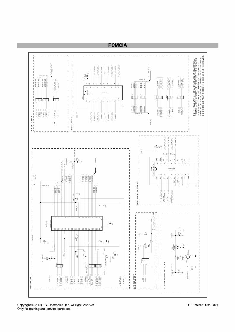
THE
S
YMBO
L M
ARK
OF
THIS
SCH
EMET
IC D
IAG
RAM
INCO
RPO
RATE
SSP
ECIA
L FE
ATUR
ES IM
PORT
ANT
FOR
PRO
TECT
ION
FRO
M X
-RAD
IATI
ON.
FILR
E AN
D EL
ECTR
ICAL
SHO
CK H
AZAR
DS, W
HEN
SERV
ICIN
G IF
IS
ESSE
NTIA
L TH
AT O
NLY
MAN
UFAT
URES
SPE
CFIE
D PA
RTS
BE U
SED
FOR
THE
CRIT
ICAL
CO
MPO
NENT
S IN
THE
SYM
BOL
MAR
K O
F TH
E SC
HEM
ETIC
.
CI_
AD
DR
[4]
CI_
DA
TA
[7]
CI_
DA
TA
[5]
CI_
AD
DR
[5]
CI_
DA
TA
[0]
CI_
DA
TA
[4]
CI_
AD
DR
[13
]
CI_
AD
DR
[7]
CI_
AD
DR
[12
]
CI_
AD
DR
[6]
CI_
AD
DR
[14
]
FE_TS_DATA[0-7]
CI_
AD
DR
[0]
CI_
AD
DR
[2]
CI_
AD
DR
[1]
CI_
AD
DR
[3]
CI_
AD
DR
[11
]
CI_
DA
TA
[6]
CI_
AD
DR
[10
]
CI_
DA
TA
[3]
CI_
AD
DR
[8]
CI_
AD
DR
[9]
CI_DATA[0-7]
CI_
DA
TA
[2]
CI_
DA
TA
[1]
CI_DATA[0-7]
CI_
DA
TA
[0]
CI_
DA
TA
[1]
CI_
DA
TA
[2]
CI_
DA
TA
[3]
CI_
DA
TA
[4]
CI_
DA
TA
[6]
CI_
DA
TA
[5]
CI_
DA
TA
[7]
PCM_D[0-7]
PC
M_
D[0
]
PC
M_
D[1
]
PC
M_
D[2
]
PC
M_
D[3
]
PC
M_
D[7
]
PC
M_
D[4
]
PC
M_
D[6
]
PC
M_
D[5
]
FE
_T
S_
DA
TA
[7]
FE
_T
S_
DA
TA
[6]
FE
_T
S_
DA
TA
[5]
FE
_T
S_
DA
TA
[4]
FE
_T
S_
DA
TA
[3]
FE
_T
S_
DA
TA
[1]
FE
_T
S_
DA
TA
[2]
FE
_T
S_
DA
TA
[0]
GN
D
CI_
DE
T
AB
9
/CI_
CD
2E
12
/CI_
CD
1
D4
CI_
MD
I[6
]
/PC
M_
WA
IT
PC
M_
D[0
-7]
CI_
IOW
R
CI_
MD
I[4
]
CI_
TS
_D
AT
A[5
]
CI_
WE
P5
00
10
06
79
72
-05
0L
F
EA
G4
18
60
10
1 G1
G2
57
21
52
16
10
47
41
5
36
59
23
45
54
18
49
43
137
38
2
25
56
20
51
159
46
40
4
35
58
22
53
17
11
48
42
126
37
1
24
55
19
50
44
148
39
3
26
60
27
61
28
62
29
63
30
64
31
32
33
34
65
66
67
68
CI_
DE
T
CI_
TS
_D
AT
A[7
]
CI_
MD
I[2
]
PC
M_
A[3
]
CI_
AD
DR
[0-1
4]
CI_
MD
I[3
]
GN
D
R5
10
10
0
CI_
MIV
AL
_E
RR
CI_
OE
/PC
M_
IOR
D
RE
G
CI_
MD
I[5
]
CI_
MD
I[4
]
R5
06
10
K
CI_
MD
I[0
]
CI_
TS
_V
AL
CI_
AD
DR
[8]
CI_
TS
_D
AT
A[1
]
/CI_
CD
1
CI_
WE
CI_
IOW
R
CI_
AD
DR
[0]
CI_
AD
DR
[6]
CI_
MD
I[2
]
R507
10KR5
08
10
K
FE
_T
S_
VA
L_
ER
R
PC
M_
A[6
]
R505
10K
PC
M_
A[1
2]
PC
M_
A[1
0]
CI_
AD
DR
[13
]
R5
16
10
0
CI_
MD
I[6
]
C5
11
0.1
uF
16
V
CI_
MD
I[3
]
CI_
AD
DR
[2]
CI_
AD
DR
[1]
C5
09
0.1
uF
16
V
PC
M_
A[7
]
C5
02
0.1
uF
16
V
GN
D
R5
11
10
0
CI_
MD
I[0
]
CI_
IOR
D
GN
D
CI_
AD
DR
[11
]
PC
M_
RS
T
/PC
M_
IRQ
A
R5
00
47
+5
V_
GE
NE
RA
L
CI_
AD
DR
[12
]
+5
V_
GE
NE
RA
L
CI_
AD
DR
[14
]
/CI_
CD
2
PC
M_
A[1
]
CI_
TS
_C
LK
PC
M_
A[8
]
CI_
OE
CI_
MIS
TR
TD
14
CI_
MD
I[7
]
CI_
MD
I[1
]
/PC
M_
WE
CI_
TS
_D
AT
A[4
]
C5
01
0.1
uF
16
V
GN
D
CI_
TS
_D
AT
A[0
]
FE
_T
S_
CL
K
CI_
MC
LK
I
RE
G
PC
M_
A[4
]C
I_M
IST
RT
PC
M_
A[9
]
FE
_T
S_
SY
N
PC
M_
A[1
3]
/PC
M_
IOW
R
R5
09
10
K
/PC
M_
OE
CI_
AD
DR
[5]
CI_
MD
I[7
]
PC
M_
A[5
]
GN
D
CI_
TS
_D
AT
A[3
]
R51710K
CI_
MIV
AL
_E
RR
GN
D
/PC
M_
RE
G
CI_
AD
DR
[3]
CI_
MD
I[5
]
/PC
M_
CE
PC
M_
A[1
1]
CI_
TS
_D
AT
A[2
]
CI_
AD
DR
[4]
+3
.3V
_C
I
PC
M_
A[0
]
PC
M_
A[2
]
CI_
AD
DR
[7]
CI_
MD
I[1
]
CI_
IOR
D
CI_
TS
_S
YN
CI_
AD
DR
[10
]
PC
M_
A[1
4]
CI_
AD
DR
[9]
FE
_T
S_
DA
TA
[0-7
]
CI_
TS
_D
AT
A[6
]
+5
V_
GE
NE
RA
L
+5
V_
CI_
ON
CI_
DA
TA
[0-7
]
CI_
DA
TA
[0-7
]
/PC
M_
CD
1:A
A1
0
R5
03
47
R5
15
47
+3
.3V
_C
I+
3.3
V_
CI
AR
50
33
3
AR
50
03
3
AR
50
4
33
AR
50
63
3
AR
50
73
3
AR
50
83
3
AR
50
93
3
AR
51
03
3
AR
51
13
3
AR
51
23
3
AR
51
33
3
CI_
MC
LK
I
IC5
02
74
LV
C5
41
A(P
W)
BUFFER3
A1
2A
0
4A
2
1O
E1
6A
4
5A
3
7A
5
8A
6
9A
7
10
GN
D1
1Y
7
12
Y6
13
Y5
14
Y4
15
Y3
16
Y2
17
Y1
18
Y0
19
OE
2
20
VC
C
+3
.3V
_C
I
FE
_T
S_
CL
KA
E5
;10
:J1
7
FE
_T
S_
VA
L_
ER
RA
E5
;10
:W1
9
FE
_T
S_
SY
NA
E5
;10
:J1
7
BU
F_
TS
_C
LK
BU
F_
TS
_V
AL
_E
RR
BU
F_
TS
_S
YN
BU
F_
TS
_D
AT
A[0
]
FE
_T
S_
DA
TA
[0]
AG
4;1
0:J
17
C510
0.1uF
16
V
C5
08
0.1
uF
C5
03
0.1
uF
C512
0.1uF
R5
21
47
R5
19
47
R518
10K
R520
10K
C5
05
10
uF
10
V
R5
22
10
K
R5
23
10
K
R5
13
0
OP
T
R5
14
0
OP
T
R5120
OPT
IC5
01
TC74LCX244FT
0IT
O7
42
44
0D
TO
SH
IBA
32
Y4
21
A1
41
A2
11
OE
61
A3
52
Y3
72
Y2
81
A4
92
Y1
10
GN
D1
12
A1
12
1Y
4
13
2A
2
14
1Y
3
15
2A
3
16
1Y
2
17
2A
4
18
1Y
1
19
2O
E
20
VC
C
IC5
00
74
LV
C1
G3
2G
W
3G
ND
2A
4Y
1B
5V
CC
R5
26
47 R5
28
47
R5
27
47
R5
25
47
R5
02
10
KQ
50
02
SC
30
52
E
B
C
C5
00
0.1
uF
16
V
+5
V_
ST
PC
M_
5V
_C
TL
Q5
01
RS
R0
25
P0
3S
D
G
+5
V_
CI_
ON
C5
07
0.1
uF
16
V
R5
01
33
K
R5
24
33
K
R5
29
2.2
K
R5
04
22
K
C5
04
10
uF
10
V
DV
B-C
I D
ET
EC
T
DV
B-C
I S
LO
TD
VB
-CI
TS
IN
PU
T
DV
B-C
I H
OS
T I
/F
DV
B-C
I S
ER
IAL
BU
FF
ER
TS
CI
PO
WE
R E
NA
BL
E C
ON
TR
OL
Copyright © 2009 LG Electronics. Inc. All right reserved. Only for training and service purposes
LGE Internal Use Only
PCMCIA
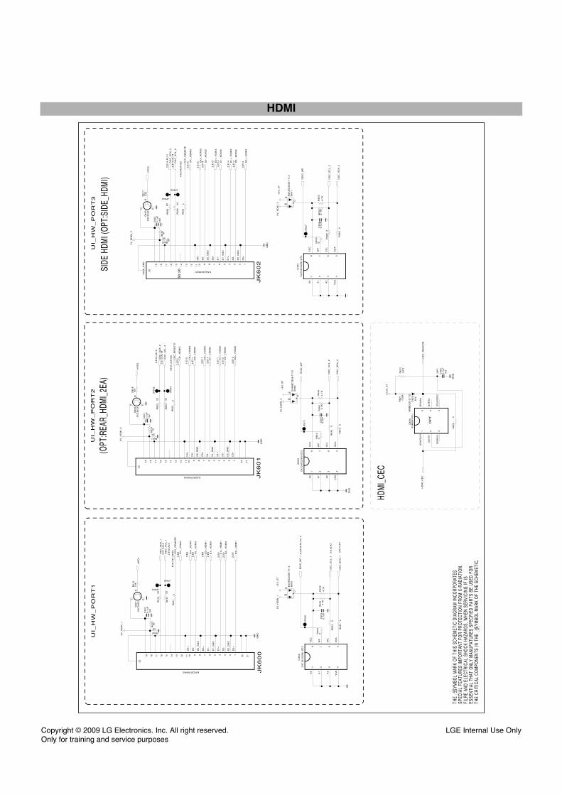
THE
SY
MBO
L M
ARK
OF
THIS
SCH
EMET
IC D
IAG
RAM
INCO
RPO
RATE
SSP
ECIA
L FE
ATUR
ES IM
PORT
ANT
FOR
PRO
TECT
ION
FRO
M X
-RAD
IATI
ON.
FILR
E AN
D EL
ECTR
ICAL
SHO
CK H
AZAR
DS, W
HEN
SERV
ICIN
G IF
IS
ESSE
NTIA
L TH
AT O
NLY
MAN
UFAT
URES
SPE
CFIE
D PA
RTS
BE U
SED
FOR
THE
CRIT
ICAL
CO
MPO
NENT
S IN
THE
S
YMBO
L M
ARK
OF
THE
SCHE
MET
IC.
GN
D
D6
01
EN
KM
C2
83
8-T
11
2
A1
C
A2
DD
C_
SD
A_
12
:E1
0;A
L9
D0
+_
HD
MI3
2:E
13
+5
V_
ST
D0
-_H
DM
I22
:E1
1
DD
C_
SD
A_
32
:E1
4;A
L1
4
CK
+_
HD
MI2
2:E
10
ED
ID_
WP
1:A
J2
0;A
I16
;AL
12
CE
C_
RE
MO
TE
K1
9;K
8;A
H2
5
DD
C_
SD
A_
2
2:E
12
;AL
19
D1
+_
HD
MI1
2:E
9
D2
-_H
DM
I22
:E1
2
JP601
ED
ID_
WP
D6
02
EN
KM
C2
83
8-T
11
2
A1
C
A2
DD
C_
SD
A_
3
DD
C_
SC
L_
3
JP
60
3
D1
+_
HD
MI2
2:E
11
D0
+_
HD
MI1
2:E
8
5V
_H
DM
I_2
DD
C_
SD
A_
12
:E1
0;K
7
JP605
D0
-_H
DM
I32
:E1
3CK
-_H
DM
I32
:E1
3
DD
C_
SC
L_
1
2:E
10
;AL
9
D1
-_H
DM
I22
:E1
1JP600
5V
_H
DM
I_3
D0
+_
HD
MI2
2:E
11
D2
+_
HD
MI3
2:E
14
GN
D
D1
-_H
DM
I12
:E9
D1
-_H
DM
I32
:E1
4 D2
-_H
DM
I32
:E1
4
CK
-_H
DM
I12
:E8 D2
+_
HD
MI1
2:E
9
+5
V_
ST
GN
D
CK
+_
HD
MI3
2:E
13
GN
D
CE
C_
RE
MO
TE
K1
9;X
14
;AH
25
CK
-_H
DM
I22
:E1
1D
DC
_S
CL
_3
2:E
15
;AL
13
D0
-_H
DM
I12
:E9
DD
C_
SC
L_
2
D1
+_
HD
MI3
2:E
14
DD
C_
SC
L_
22
:E1
2;A
L1
8
D2
-_H
DM
I12
:E9
JP
60
6
DD
C_
SC
L_
12
:E1
0;K
7
+5
V_
ST
CE
C_
RE
MO
TE
K8
;X1
4;A
H2
5
JP604
D6
00
EN
KM
C2
83
8-T
11
2
A1
C
A2
DD
C_
SD
A_
2
5V
_H
DM
I_1
D2
+_
HD
MI2
2:E
12
CK
+_
HD
MI1
2:E
8
JP
61
1E
DID
_W
P
JP
60
7
5V
_H
DM
I_1
HP
D1
Q6
01
2S
C3
05
2
E
B
C
5V
_H
DM
I_2
HP
D2
Q6
02
2S
C3
05
2
E
B
C5
V_
HD
MI_
3
HP
D3
Q6
03
2S
C3
05
2
E
B
C
IC6
01
CA
T2
4C
02
WI-
GT
3
3A
2
2A
1
4V
SS
1A
0
5S
DA
6S
CL
7W
P
8V
CC
IC6
00
CA
T2
4C
02
WI-
GT
3
3A
2
2A
1
4V
SS
1A
0
5S
DA
6S
CL
7W
P
8V
CC
IC6
02
CA
T2
4C
02
WI-
GT
3
3A
2
2A
1
4V
SS
1A
0
5S
DA
6S
CL
7W
P
8V
CC
R6
07
0
GN
D
+3
.3V
_S
T
HD
MI_
CE
C
Q6
00
SS
M6
N1
5F
U
OP
T
3D
RA
IN2
2G
AT
E1
1S
OU
RC
E1
4S
OU
RC
E2
5G
AT
E2
6D
RA
IN1
D6
03
MM
BD
30
1L
T1
G
30
V
CE
C_
RE
MO
TE
R6
25
0
C6
05
0.1
uF
16
V
OP
T
R6
27
12
0K
C6
00
0.1
uF
16
V
C6
01
0.1
uF
16
V
C6
02
0.1
uF
16
V
C6
03
0.1
uF
C6
04
0.1
uF
C6
07
0.1
uF
R600
2K
R601
2K
R602
2K
R6
03
22
R6
09
0
R6
18
0
R6
19
0
R6
20
0
R6
21
0R
62
20
R6
45
0
R6
42
0
R6
40
0
R6
23
0
R6
05
0
R6
17
10
K
R6
16
10
KR
61
51
0K
R6
13
1K
R6
14
1K
R6
12
1K
R6
06
22
R6
04
22
R6
10
22
R6
11
22
R6
08
22
R6
31
OP
T
JP
60
2
R6
46
4.7
K
R6
49
4.7
KR
62
84
.7
KR
62
64
.7K
R6
30
4.7
KR
62
9
4.7
K
JK
60
1
EAG39789402
1D
2+
2D
2_
GN
D
3D
2-
4D
1+
5D
1_
GN
D
6D
1-
7D
0+
8D
0_
GN
D
9D
0-
10
CK
+1
1
12
13
14
15
16
17
18
19
20
21
22
JK
60
0
EAG39789402
1D
2+
2D
2_
GN
D
3D
2-
4D
1+
5D
1_
GN
D
6D
1-
7D
0+
8D
0_
GN
D
9D
0-
10
CK
+1
1
12
13
14
15
16
17
18
19
20
21
22
JK
60
2
EAG42463001
14
13 5
D1
_G
ND
20
JA
CK
_G
ND
12
11 2
D2
_G
ND
19
18
10
CK
+
4D
1+
1D
2+
17 9
D0
-
8D
0_
GN
D
3D
2-
16 7
D0
+
6D
1-
15
UI_
HW
_P
OR
T3
UI_
HW
_P
OR
T1
UI_
HW
_P
OR
T2
SIDE
HDM
I (OP
T:SI
DE_H
DMI)
$0
.26
(OPT
:REA
R_HD
MI_
2EA)
HDM
I_CE
C
Copyright © 2009 LG Electronics. Inc. All right reserved. Only for training and service purposes
LGE Internal Use Only
HDMI
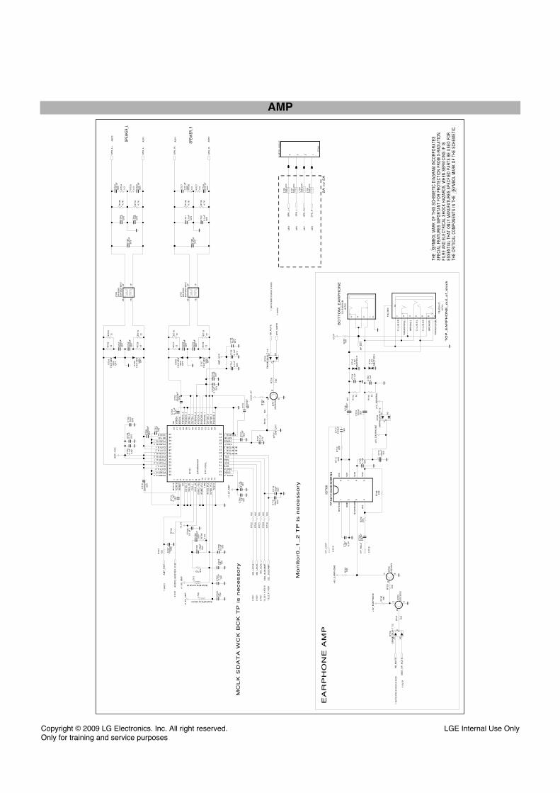
THE
SY
MBO
L M
ARK
OF
THIS
SCH
EMET
IC D
IAG
RAM
INCO
RPO
RATE
SSP
ECIA
L FE
ATUR
ES IM
PORT
ANT
FOR
PRO
TECT
ION
FRO
M X
-RAD
IATI
ON.
FILR
E AN
D EL
ECTR
ICAL
SHO
CK H
AZAR
DS, W
HEN
SERV
ICIN
G IF
IS
ESSE
NTIA
L TH
AT O
NLY
MAN
UFAT
URES
SPE
CFIE
D PA
RTS
BE U
SED
FOR
THE
CRIT
ICAL
CO
MPO
NENT
S IN
THE
S
YMBO
L M
ARK
OF
THE
SCHE
MET
IC.
0.1
uF
C7
29
50
V
0.1
uF
C7
49
50
V
0.1
uF
C7
35
50
V
SP
K_
R+
AB
11
R7
34
3.3
C7
32
22
00
0p
F5
0V
C7
46
0.4
7u
F5
0V
SP
K_
R-
AB
12
MS
_L
RC
K2
:X2
1
AM
P_
VC
C
0.0
1u
FC
75
8
50
V
R7
36
3.3
0.1
uF
C7
28
50
V
0.0
1u
FC
75
6
50
V
R7
30
4.7
K
0.1
uF
C7
33
50
V
0.0
1u
F
C7
57
50
V
L7
04
DA
-85
80
EA
P3
83
19
00
12
S
1S
1F
2F
SD
A_
SU
B/A
MP
1:L
22
;11
:AG
10
SP
K_
L-
AB
11
0.1
uF
C7
50
50
V
R7
37
3.3
R7
32
4.7
K
MS
_L
RC
H2
:X2
1
SP
K_
L+
AB
10
MS
_S
CK
2:X
21
AU
DIO
_M
AS
TE
R_
CL
K2
:X2
1
0.1
uF
C7
34
50
V
C7
31
22
00
0p
F5
0V
+1
.8V
_A
MP
C7
26
22
00
0p
F5
0V
+1
.8V
_A
MP
C7
45
0.4
7u
F5
0V
0.1
uF
C7
52
50
V
0.1
uF
C7
51
50
V
AM
P_
RS
T1
:AA
21
L7
05
DA
-85
80
EA
P3
83
19
00
12
S
1S
1F
2F
0.0
1u
FC
75
5
50
V
R7
35
3.3
SC
L_
SU
B/A
MP
1:L
22
;11
:AG
9
R7
33
4.7
K
C7
16
22
00
0p
F5
0V
R7
31
4.7
K
+1
.8V
_A
MP
SP
K_
R-
AE
9
SP
K_
L-
AE
5
SP
K_
L+
AE
3
SP
K_
R+
AE
7
HP
_R
OU
T
2:X
19
C7
19
10
0u
F1
6V
HP
_L
OU
T
2:X
19
IC7
00
TP
A6
11
0A
2D
GN
RG
4
3S
HU
TD
OW
N
2G
ND
4IN
2-
1B
YP
AS
S
5V
O2
6V
DD
7V
O1
8IN
1-
C7
18
10
0u
F1
6V
Q7
00
2S
C3
05
2
E
B
C
+5
V_
EA
RP
HO
NE
P7
00
WA
FE
R-A
NG
LE
1234
C7
03
0.2
2u
F1
6V
C7
17
0.2
2u
F
16
V
+3
.3V
Q7
01
2S
C3
05
2
E
B
C
+3
.3V
_S
T
AM
P_
VC
C
JK
70
0D
J-S
36
00
LM
BO
TT
OM
_E
AR
PH
ON
E
1234 5
+3
.3V
HP
_D
ET
SID
E_
HP
_M
UT
E1
:AJ
19
D7
08
EN
KM
C2
83
8-T
11
2A
1
C
A2
SB
_M
UT
E1
:AA
19
;R1
5;9
:AI2
4;9
:AI2
5
SB
_M
UT
E1
:AA
19
;G2
5;9
:AI2
4;9
:AI2
5
NT
P_
MU
TE
1:A
A2
2
D7
09
EN
KM
C2
83
8-T
11
2A
1
C
A2
R7
22
10
0
R7
20
10
0
R7
21
10
0
D7
04
10
0V
1N
41
48
W
OP
T
D7
05
10
0V
1N
41
48
W
OP
T
D7
06
10
0V
1N
41
48
W
OP
T
D7
07
10
0V
1N
41
48
W
OP
T
D7
10
5.6
VA
MO
TE
CH
D7
11
5.6
VA
MO
TE
CH
L7
00
BLM18PG121SN1DL
70
1
BLM18PG121SN1D
C7
12
33
pF
50
V
C7
14
33
pF
50
V
R7
10
10
0
R7
09
10
0
R7
26
12
R7
27
12
R7
25
12
R7
28
12
R7
16
12
R7
05
12
R7
13
12
R7
19
12
C7
25
10
uF
35
V
C7
36
10
uF
35
V
+5
V_
EA
RP
HO
NE
Q7
05
2S
C3
05
2
E
B
C
R7
40
0
R7030
0.1
uF
C7
09
C7
10
0.1
uF
16
V
C7
02
0.1
uF
16
V
0.1
uF
C7
15
16
V
0.1
uF
C7
06
16
V
R7
04
10
0
C7
41
10
00
pF
50
V
C7
07
10
00
pF
50
V
C7
08
10
00
pF
50
V
C7
43
10
00
pF
50
V
C7
42
10
00
pF
50
V
C7
44
10
00
pF
50
VC
70
5
10
0p
F5
0V
R7
00
10
K
R7
24
10
K
R7
29
10
K
R7
07
10
K
R7
41
10
K
R7
14 1K
R7
15 1K
C7
01
1u
F6
.3V
R7
08
3.3
K
R7
17 33
KO
PT
+5
V_
GE
NE
RA
L+
5V
_E
AR
PH
ON
E
C7
11
10
0u
F1
6V
D7
00
EN
KM
C2
83
8-T
11
2A
1
C
A2
R7
42
10
K
R7
01
10
K
R7
11
20
K
R7
02
20
K
R7
12
20
K
R7
06
20
K
IC7
01
NT
P-3
10
0L
EA
N6
06
64
00
1
1B
ST
1A
2V
DR
1A
3R
ES
ET
4A
D
5D
VS
S_
1
6V
SS
_IO
7C
LK
_I
8V
DD
_IO
9D
GN
D_
PL
L
10
AG
ND
_P
LL
11
LF
M
12
AV
DD
_P
LL
13
DV
DD
_P
LL
14
TE
ST
0
15 DVSS_2
16 DVDD
17 SDATA
18 WCK
19 BCK
20 SDA
21 SCL
22 MONITOR_0
23 MONITOR_1
24 MONITOR_2
25 FAULT
26 VDR2B
27 BST2B
28 PGND2B_1
29
PG
ND
2B
_2
30
OU
T2
B_
13
1O
UT
2B
_2
32
PV
DD
2B
_1
33
PV
DD
2B
_2
34
PV
DD
2A
_1
35
PV
DD
2A
_2
36
OU
T2
A_
13
7O
UT
2A
_2
38
PG
ND
2A
_1
39
PG
ND
2A
_2
40
BS
T2
A4
1V
DR
2A
42
NC
43VDR1B44BST1B45PGND1B_146PGND1B_247OUT1B_148OUT1B_249PVDD1B_150PVDD1B_251PVDD1A_152PVDD1A_253OUT1A_154OUT1A_255PGND1A_156PGND1A_2
C7
23
0.1
uF
C7
22
0.1
uF
JK
70
1
PE
J0
26
-01
TO
P_
EA
RP
HO
NE
_o
ut_
of_
sto
ck
3T
RA
NS
FE
R[L
]
4B
RE
AK
[L]
5C
-LU
G-E
L
6C
-LU
G-E
S
7C
-LU
G-E
R
8B
RE
AK
[R]
9T
RA
NS
FE
R[R
]
10
FIX
-TE
R
L7
09
12
0-o
hm
L7
06
12
0-o
hm
L7
08
12
0-o
hm
L7
07
12
0-o
hm
C7
27
0.1
uF
16
V
C7
13
0.
1u
F1
6V
C7
24
0.
1u
F1
6V
C7
30
0.
1u
F1
6V
C7
00
1u
F1
0V
C7
04
1u
F1
0V
C7
60
1u
F1
0V
R7
18
10
0
C7
21
0.1
uF
16
V
0.1
uF
C7
20
50
V
SPEA
KER_
L
SPEA
KER_
R
EA
RP
HO
NE
AM
P
2A
=>
5A
MC
LK
SD
AT
A W
CK
BC
K T
P i
s n
ece
sso
ry
Mo
nit
or0
_1
_2
TP
is n
ece
sso
ry
Copyright © 2009 LG Electronics. Inc. All right reserved. Only for training and service purposes
LGE Internal Use Only
AMP

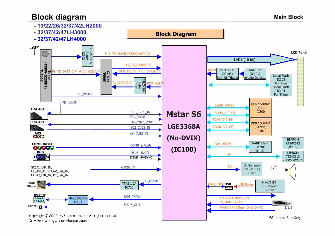
Block Diagram Block Diagram
RGB
COMPONENT
F-SCART
AV3
BUF_TS_CLK/ERR/SYN/DATA[0]
AV_CVBS_IN
DDR2 SDRAM(1Gb)IC300
NAND FlashHYNIXIC102
USB
Digital amp(NTP3100L)
IC701
COMP_Y/Pb/Pr
SC1_CVBS_IN
SC2_CVBS_IN
I2S
DSUB_ R/G/B
Tu
ner
(TD
FW-G
23
5D
1)
TU
10
00
LCD Panel
- 19/22/26/32/37/42LH2000- 32/37/42/47LH3000- 32/37/42/47LH4000
74LVC541ABufferIC502
CI S
lot
(P5
00
)
74LCX244BufferIC501
PCM_A[0:7]
FE_VMAIN
PCM_A[0:7]
SDDR_D[0:15]
DDR2 SDRAM(512Mb)IC301
TDDR_D[0:15]
SDDR_A[0:12]Mstar S6LGE3368A
(No-DVIX)
(IC100)
MP6211DHUSB Power
IC402
USB Power
FE_TS_DATA[0:7] CI_MDI[0:7]
H-SCART
SC1_R/G/B
SC1/2_L/R_IN,FE_AM_AUDIO,AV_L/R_IN,COMP_L/R_IN, PC_L/R_IN
FE_ VOUT
DTV/MNT_VOUTTDDR_A[0:12]
TPA6110AIC700
Head Phone
RS-232CMAX3232CDR
IC403SPDIF SPDIF_OUT
DSUB_H/VSYNC
HP_L/ROUT
L/R
CI_TS_DATA[0:7]
PCM_D[0:7] CI_DATA[0:7]
CI_ADDR[0:7]
AUDIO IN
DGB_TX/RX HPD1/2/3, HDMI_CEC
TMDS[0:7] ( Data, Clock (+/-))
USB_DM/DP
EEPROMAT24C512(IC105)
EEPROMAT24C512
(HDCP)IC107
I2C
LVDS (10 bit)
Serial FlashIC104
For Triton
Serial FlashIC103
For Boot
KIA7027(IC101)
Voltage Detector
74LX1G14C(IC108)
Schmitt Trigger
Reset
5V_HDMI_1/2/3 HDMI1/2/3
Block diagram Main Block
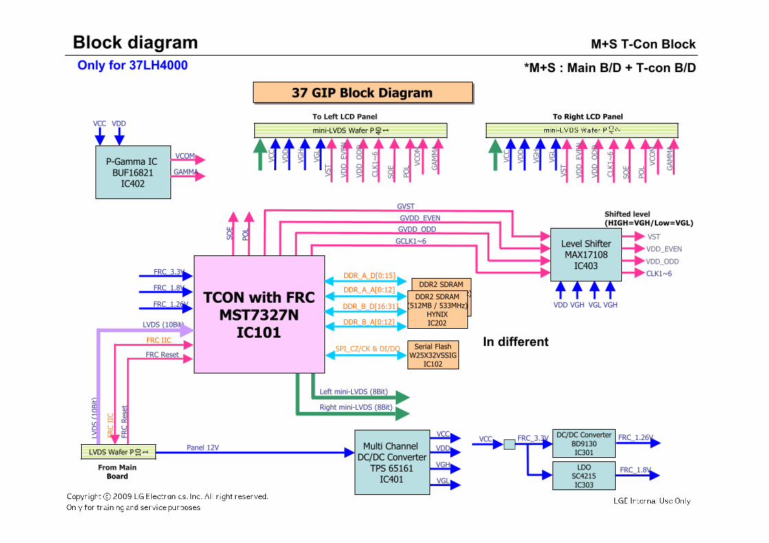
37 GIP Block Diagram37 GIP Block Diagram
TCON with FRCMST7327N
IC101
M+S T-Con Block
SPI_CZ/CK & DI/DO
DDR_A_D[0:15]DDR2 SDRAM
(512MB / 533MHz)HYNIXIC201
DDR_B_D[16:31]
DDR_A_A[0:12]
DDR_B_A[0:12]
Serial FlashW25X32VSSIG
IC102
DDR2 SDRAM(512MB / 533MHz)
HYNIXIC202
Multi Channel DC/DC Converter
TPS 65161IC401
P-Gamma IC BUF16821
IC402
VCC
VDD
VGH
VGL
VCC VDD
Level ShifterMAX17108
IC403
GVST
GVDD_EVEN
GVDD_ODD
GCLK1~6
VGHVGLVGHVDD
SOE
POL
Left mini-LVDS (8Bit)
Right mini-LVDS (8Bit)
LVDS (10Bit)
FRC IIC
FRC Reset
VCOM
GAMMA
FRC_3.3V
FRC_1.8V
FRC_1.26V
DC/DC ConverterBD9130IC301
LDOSC4215IC303
FRC_1.8V
FRC_1.26VFRC_3.3VVCCLVD
S (1
0Bit)
From MainBoard
FRC
IIC
FRC
Res
et
Panel 12V
To Left LCD Panel To Right LCD Panel
VST
VDD_EVEN
VDD_ODD
CLK1~6
Shifted level(HIGH=VGH/Low=VGL)
VCC
VDD
VGH
VGL
VST
VDD
_EVE
N
VDD
_OD
D
CLK1
~6
SOE
POL VC
OM
GAM
MA
VCC
VDD
VGH
VGL
VST
VDD
_EVE
N
VDD
_OD
D
CLK1
~6
SOE
POL VC
OM
GAM
MA
LVDS Wafer P 10 1
mini-LVDS Wafer P 40 1
Only for 37LH4000
Block diagram*M+S : Main B/D + T-con B/D
In different
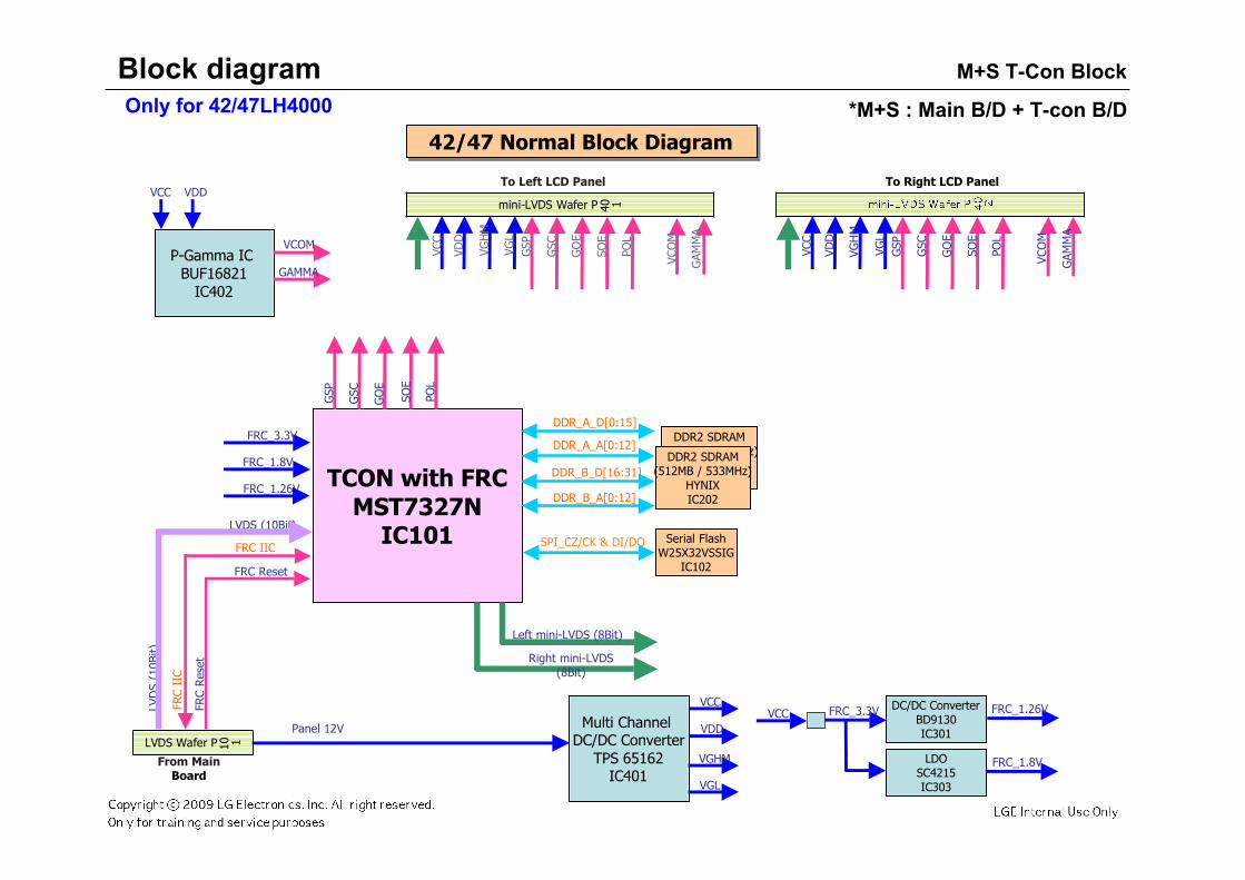
42/47 Normal Block Diagram42/47 Normal Block Diagram
TCON with FRCMST7327N
IC101 SPI_CZ/CK & DI/DO
DDR_A_D[0:15]DDR2 SDRAM
(512MB / 533MHz)HYNIXIC201
DDR_B_D[16:31]
DDR_A_A[0:12]
DDR_B_A[0:12]
Serial FlashW25X32VSSIG
IC102
DDR2 SDRAM(512MB / 533MHz)
HYNIXIC202
Multi Channel DC/DC Converter
TPS 65162IC401
P-Gamma IC BUF16821
IC402
VCC
VDD
VGL
VCC VDD
GSP
GSC
GO
E
SOE
POL
VCOM
GAMMA
DC/DC ConverterBD9130IC301
LDOSC4215IC303
FRC_1.8V
FRC_1.26VFRC_3.3VVCC
VGHM
Left mini-LVDS (8Bit)
Right mini-LVDS(8Bit)
LVDS (10Bit)
FRC IIC
FRC Reset
FRC_3.3V
FRC_1.8V
FRC_1.26V
LVDS Wafer P 10 1
LVD
S (1
0Bit)
FRC
IIC
FRC
Res
et
Panel 12V
mini-LVDS Wafer P 40 1
To Left LCD Panel To Right LCD Panel
VCC
VDD
VGH
M
VGL
GSP
GSC
GO
E
SOE
POL
VCO
M
GAM
MA
VCC
VDD
VGH
M
VGL
GSP
GSC
GO
E
SOE
POL
VCO
M
GAM
MA
From MainBoard
Only for 42/47LH4000
Block diagram M+S T-Con Block
*M+S : Main B/D + T-con B/D
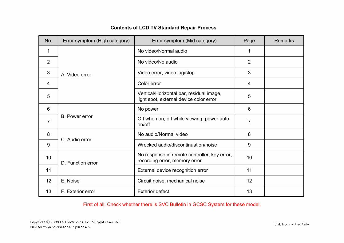
Contents of LCD TV Standard Repair Process
No. Error symptom (High category) Error symptom (Mid category) Page Remarks
1
A. Video error
No video/Normal audio 1
2 No video/No audio 2
3 Video error, video lag/stop 3
4 Color error 4
5Vertical/Horizontal bar, residual image,light spot, external device color error
5
6
B. Power error
No power 6
7Off when on, off while viewing, power autoon/off
7
8C. Audio error
No audio/Normal video 8
9 Wrecked audio/discontinuation/noise 9
10D. Function error
No response in remote controller, key error,recording error, memory error
10
11 External device recognition error 11
12 E. Noise Circuit noise, mechanical noise 12
13 F. Exterior error Exterior defect 13
First of all, Check whether there is SVC Bulletin in GCSC System for these model.
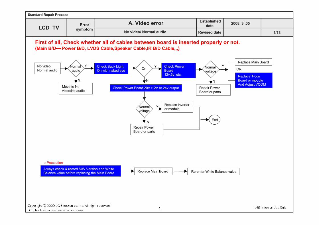
Normal audio
Y
N
Move to Novideo/No audio
No videoNormal audio
Check Back LightOn with naked eye
OnY
N
Check PowerBoard12v,5v etc.
Normal voltage
Y
N
Replace Main Board
Replace T-conBoard or moduleAnd Adjust VCOM
OR
Repair PowerBoard or parts
Check Power Board 20V /12V or 24v output
Normalvoltage
YReplace Inverteror module
N
Repair PowerBoard or parts
End
Always check & record S/W Version and WhiteBalance value before replacing the Main Board Replace Main Board Re-enter White Balance value
Precaution
Establisheddate
Standard Repair Process
Revised date
2008. 3 .05
1/13LCD TV
Errorsymptom
A. Video error
No video/ Normal audio
First of all, Check whether all of cables between board is inserted properly or not.(Main B/D Power B/D, LVDS Cable,Speaker Cable,IR B/D Cable,,,)
1
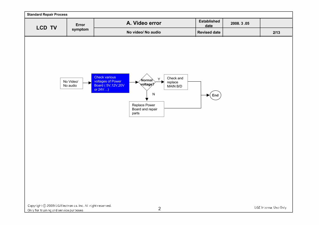
Normal voltage?
Check variousvoltages of PowerBoard ( 5V,12V,20Vor 24V…)
No Video/No audio
Check andreplaceMAIN B/D
Y
Replace PowerBoard and repairparts
N End
Standard Repair Process
A. Video error
No video/ No audio
Establisheddate
Revised date
2008. 3 .05
2/13LCD TV
Errorsymptom
2
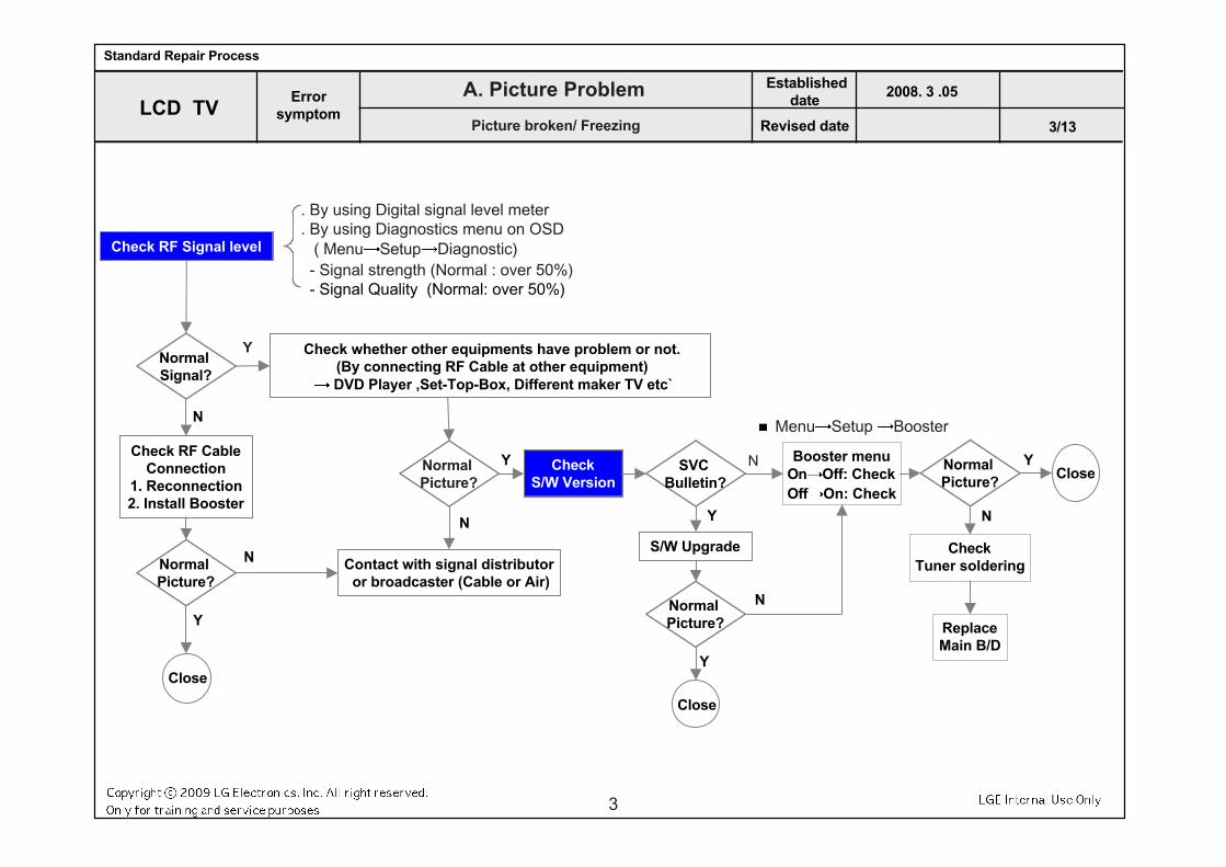
A. Picture Problem
Picture broken/ Freezing
Y
N
N
Check RF Signal level
Normal Signal?
Check RF CableConnection
1. Reconnection2. Install Booster
CheckS/W Version
Booster menuOn Off: CheckOff On: Check
S/W Upgrade
Check whether other equipments have problem or not. (By connecting RF Cable at other equipment)
DVD Player ,Set-Top-Box, Different maker TV etc`
SVC Bulletin?
ReplaceMain B/D
CheckTuner soldering
Normal Picture?
Y
N
Y
Close
Normal Picture?
YClose
Menu Setup Booster
. By using Digital signal level meter
. By using Diagnostics menu on OSD ( Menu Setup Diagnostic) - Signal strength (Normal : over 50%) - Signal Quality (Normal: over 50%)
Normal Picture?
Y
Contact with signal distributor or broadcaster (Cable or Air)
N N
Normal Picture?
Y
Close
N
Standard Repair Process
Establisheddate
Revised date
2008. 3 .05
3/13LCD TV
Errorsymptom
3
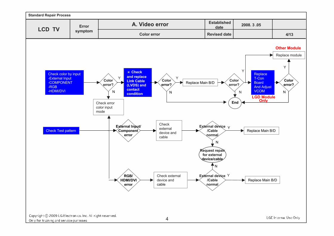
Colorerror?
Y
N
Checkand replaceLink Cable(LVDS) andcontactcondition
Y
N
Replace Main B/DColorerror?
Check errorcolor inputmode
Check color by input-External Input-COMPONENT-RGB-HDMI/DVI
YExternal device/Cablenormal
External Input/Component
error
Checkexternaldevice andcable
YExternal device/Cablenormal
RGB/HDMI/DVI
error
Check externaldevice andcable
Replace Main B/D
Replace Main B/D
N
N
A. Video error
Color error
N
Y
End
Replace module
Request repairfor externaldevice/cable
Replace T-Con BoardAnd AdjustVCOM N
Y
Colorerror?
LGD ModuleOnly
Other Module
Colorerror?
Check Test pattern
Standard Repair Process
Establisheddate
Revised date
2008. 3 .05
4/13LCD TV
Errorsymptom
4
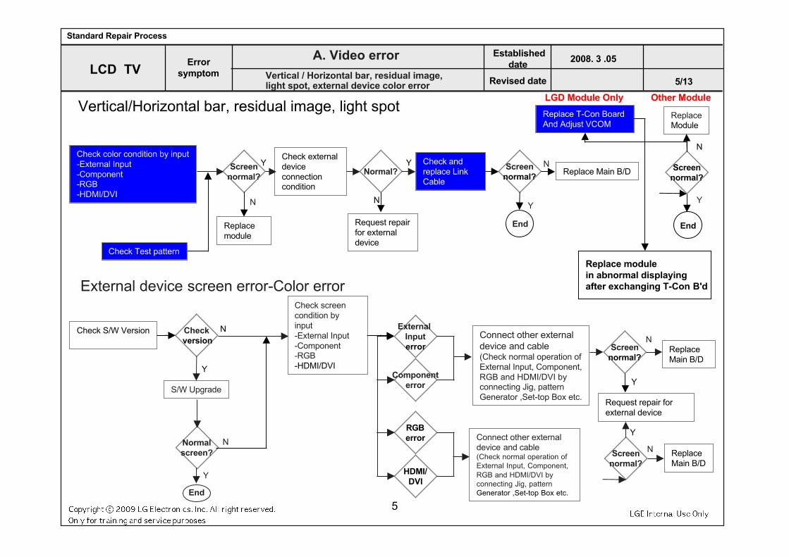
Screennormal?
N
YCheck externaldeviceconnectioncondition
Y
N
Check andreplace LinkCable
Normal?
Y
NScreennormal?
Replace Main B/D
Replacemodule
Check color condition by input-External Input-Component-RGB-HDMI/DVI
End
Vertical/Horizontal bar, residual image, light spot
Request repairfor externaldevice
A. Video error
Vertical / Horizontal bar, residual image, light spot, external device color error
External device screen error-Color error
External Inputerror
Connect other externaldevice and cable(Check normal operation ofExternal Input, Component,RGB and HDMI/DVI byconnecting Jig, patternGenerator ,Set-top Box etc.
N
Y
ReplaceMain B/D
Screennormal?
Check screencondition byinput-External Input-Component-RGB-HDMI/DVI
Request repair forexternal device
Componenterror
RGBerror
HDMI/DVI
Connect other externaldevice and cable(Check normal operation ofExternal Input, Component,RGB and HDMI/DVI byconnecting Jig, patternGenerator ,Set-top Box etc.
Replace Main B/D
Screennormal?
N
Y
Check S/W Version
Y
NCheck version
S/W Upgrade
Y
NNormalscreen?
End
Y
N
Replace T-Con BoardAnd Adjust VCOM
LGD Module Only
ReplaceModule
Other Module
Replace modulein abnormal displayingafter exchanging T-Con B'd
Screennormal?
End
Establisheddate
Revised date
2008. 3 .05
5/13LCD TV
Errorsymptom
Standard Repair Process
Check Test pattern
5
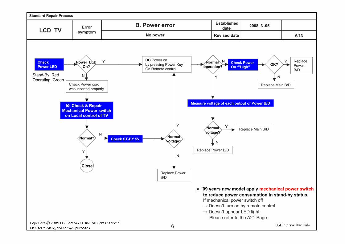
B. Power error
No power
Power LEDOn?
Y
N
DC Power onby pressing Power KeyOn Remote control
Y
NNormal operation?
Check PowerOn ‘”High”
Check Power cordwas inserted properly
CheckPower LED
ReplacePowerB/D
Measure voltage of each output of Power B/D
N
YNormalvoltage?
Replace Main B/D
N
YOK?
Replace Main B/D
N
Y
Normal? Check ST-BY 5V
Replace Power B/D
N
YNormal
voltage?
Replace PowerB/D
Y
Standard Repair Process
Establisheddate
Revised date
2008. 3 .05
6/13LCD TV
Errorsymptom
’09 years new model apply mechanical power switch to reduce power consumption in stand-by status. If mechanical power switch off Doesn’t turn on by remote control Doesn’t appear LED light Please refer to the A21 Page
6
. Stand-By: Red
. Operating: Green
Check & RepairMechanical Power switch
on Local control of TV
Close
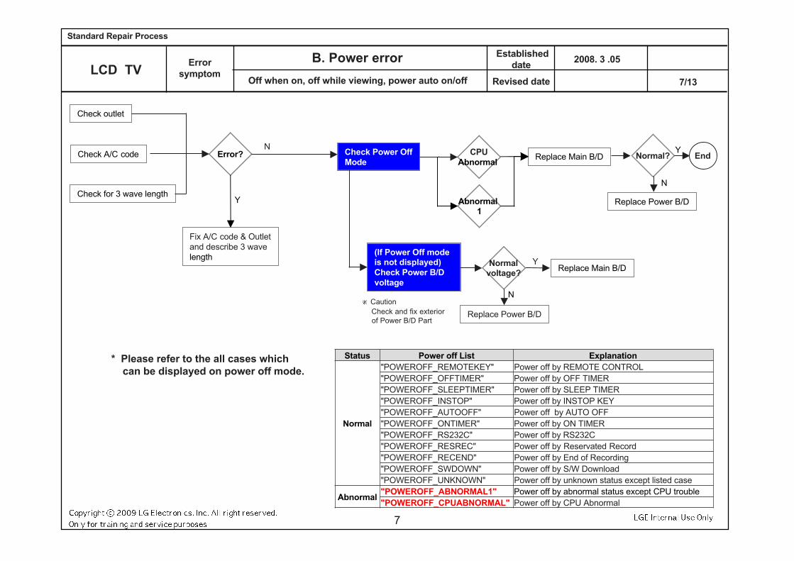
B. Power error
Off when on, off while viewing, power auto on/off
Error?N
Y
Check Power OffMode
Fix A/C code & Outletand describe 3 wavelength
Check A/C code
Check for 3 wave length
Check outlet
Replace Main B/DCPUAbnormal
(If Power Off modeis not displayed)Check Power B/Dvoltage
Y
N
Replace Main B/DNormal
voltage?
Replace Power B/D
Replace Power B/D
N
YNormal? End
Caution Check and fix exterior of Power B/D Part
Establisheddate
Revised date
2008. 3 .05
7/13LCD TV
Errorsymptom
Standard Repair Process
7
Status Power off List Explanation
Normal
"POWEROFF_REMOTEKEY" Power off by REMOTE CONTROL"POWEROFF_OFFTIMER" Power off by OFF TIMER"POWEROFF_SLEEPTIMER" Power off by SLEEP TIMER"POWEROFF_INSTOP" Power off by INSTOP KEY"POWEROFF_AUTOOFF" Power off by AUTO OFF"POWEROFF_ONTIMER" Power off by ON TIMER"POWEROFF_RS232C" Power off by RS232C"POWEROFF_RESREC" Power off by Reservated Record"POWEROFF_RECEND" Power off by End of Recording"POWEROFF_SWDOWN" Power off by S/W Download"POWEROFF_UNKNOWN" Power off by unknown status except listed case
Abnormal"POWEROFF_ABNORMAL1" Power off by abnormal status except CPU trouble"POWEROFF_CPUABNORMAL" Power off by CPU Abnormal
* Please refer to the all cases which can be displayed on power off mode.
Abnormal 1
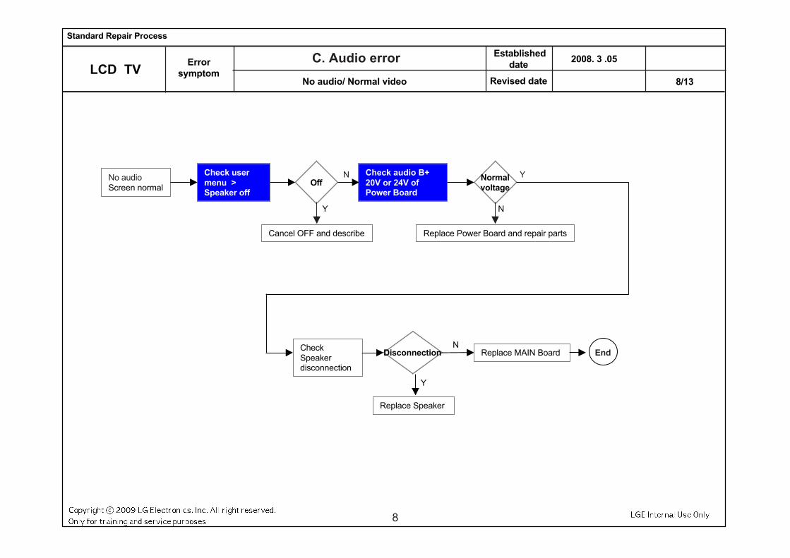
No audioScreen normal
Check usermenu >Speaker off
OffN
Y
Cancel OFF and describe
Check audio B+20V or 24V ofPower Board
Normalvoltage
Y
N
Replace Power Board and repair parts
CheckSpeakerdisconnection
N
Y
Replace Speaker
Replace MAIN Board End
C. Audio error
No audio/ Normal video
Disconnection
Establisheddate
Revised date
2008. 3 .05
8/13LCD TV
Errorsymptom
Standard Repair Process
8
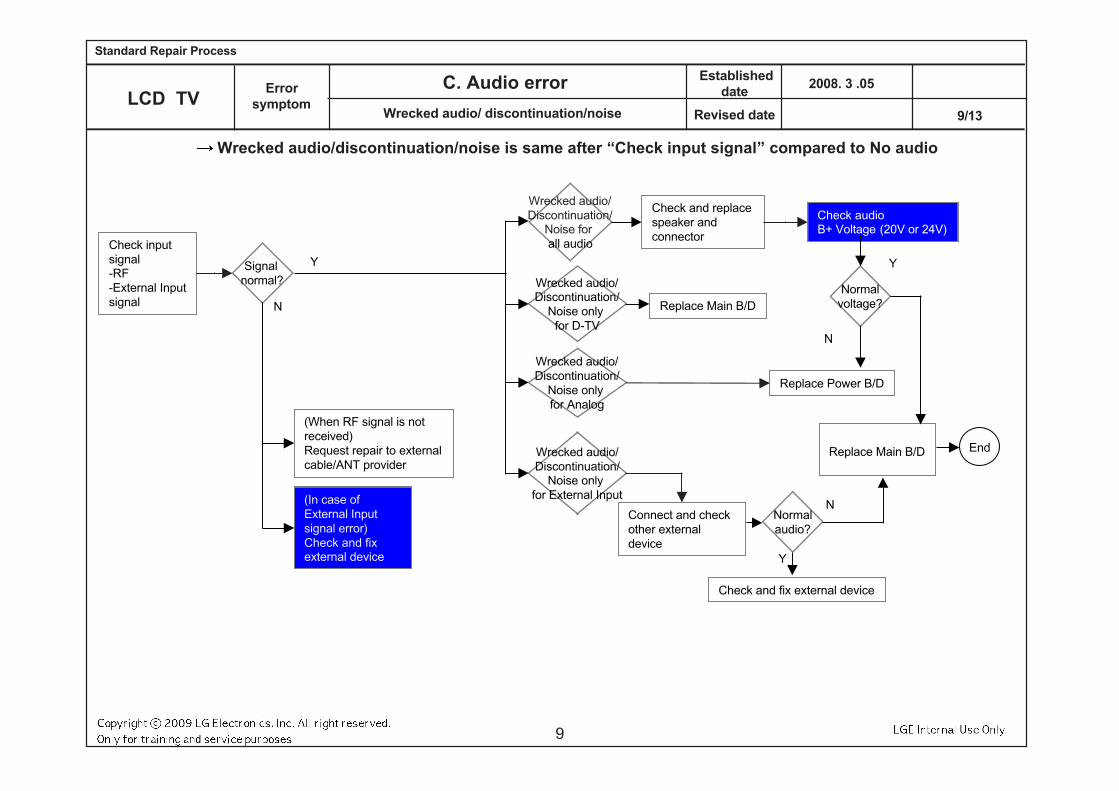
Wrecked audio/discontinuation/noise is same after “Check input signal” compared to No audio
C. Audio error
Wrecked audio/ discontinuation/noise
Wrecked audio/Discontinuation/
Noise for all audio
Check and replacespeaker andconnector
Wrecked audio/Discontinuation/
Noise only for D-TV
Wrecked audio/Discontinuation/
Noise only for Analog
Wrecked audio/Discontinuation/
Noise only for External Input
Connect and checkother externaldevice
N
Y
Normalaudio?
Check and fix external device
Replace Power B/D
N
Y
Normalvoltage?
Check inputsignal-RF-External Inputsignal
Signal normal?
(When RF signal is notreceived)Request repair to externalcable/ANT provider
Y
Check audio B+ Voltage (20V or 24V)
Replace Main B/D
(In case ofExternal Inputsignal error)Check and fixexternal device
Replace Main B/DN
End
Establisheddate
Revised date
2008. 3 .05
9/13LCD TV
Errorsymptom
Standard Repair Process
9
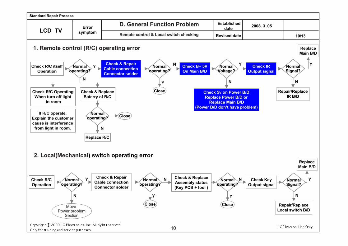
D. General Function Problem
Remote control & Local switch checking
Y
N
1. Remote control (R/C) operating error
Move Power problem
Section
2. Local(Mechanical) switch operating error
Check R/C itselfOperation
Normaloperating?
Normaloperating?
Y
Close
Replace R/C
If R/C operate,Explain the customercause is interferencefrom light in room.
Check R/C OperatingWhen turn off light
in room
Check & ReplaceBaterry of R/C
Check & RepairCable connectionConnector solder
Normaloperating?
Check B+ 5VOn Main B/D
NormalVoltage?
Close
N
N
Check 5v on Power B/DReplace Power B/D or
Replace Main B/D(Power B/D don’t have problem)
Check IROutput signal
NormalSignal?
N
Y
Repair/ReplaceIR B/D
N
ReplaceMain B/D
Y
Y
N
Check R/COperation
Normaloperating?
Y
Check & RepairCable connectionConnector solder
Normaloperating?
Close
N Check & ReplaceAssembly status(Key PCB + tool )
Check KeyOutput signal
Y
Normaloperating?
Close
N NormalSignal?
Repair/ReplaceLocal switch B/D
N
ReplaceMain B/D
Y
Standard Repair Process
Establisheddate
Revised date
2008. 3 .05
10/13LCD TV
Errorsymptom
10
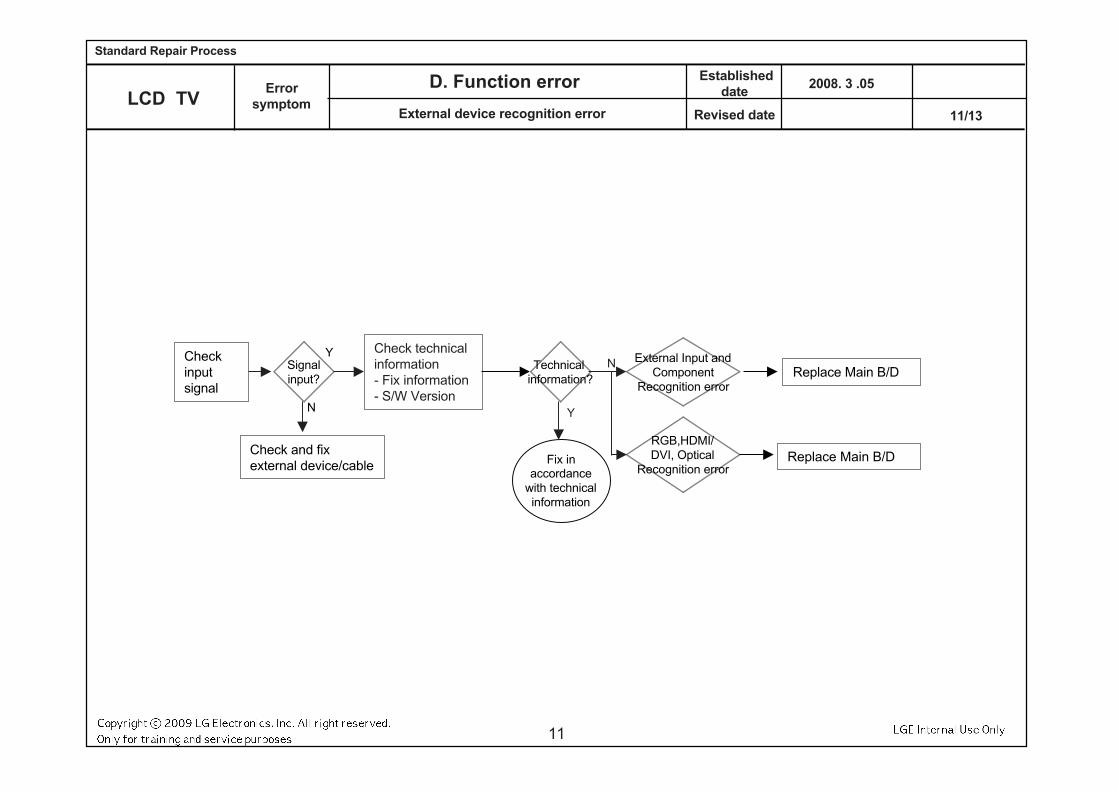
Check technicalinformation- Fix information- S/W Version
N
Y
Technical information?
Checkinputsignal
Signalinput?
Y
N
External Input andComponent
Recognition error
Check and fix external device/cable
RGB,HDMI/DVI, Optical
Recognition error
Replace Main B/D
Replace Main B/DFix inaccordance
with technicalinformation
D. Function error
External device recognition error
Establisheddate
Revised date
2008. 3 .05
11/13LCD TV
Errorsymptom
Standard Repair Process
11
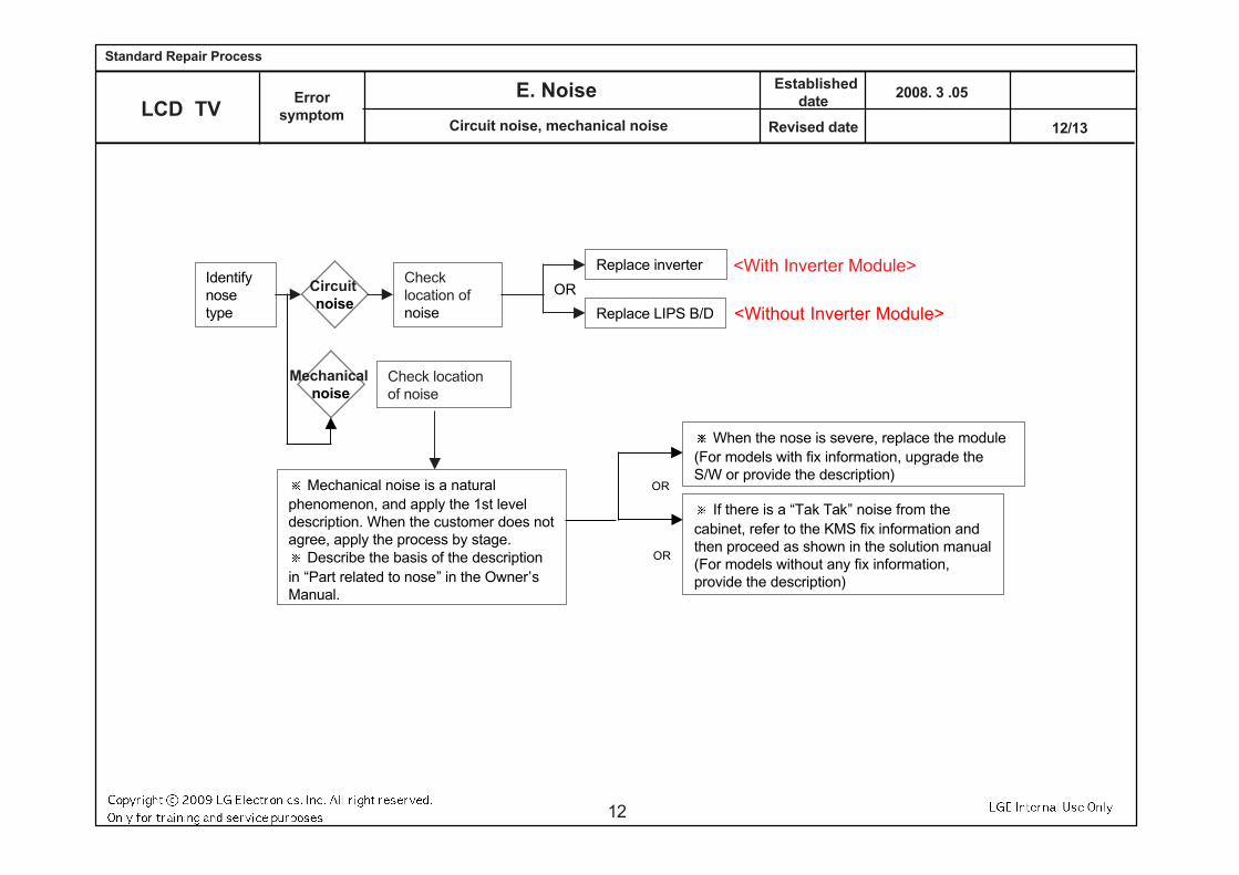
Checklocation ofnoise
Identifynosetype
Circuit noise
Replace inverter
Replace LIPS B/D
Mechanical noise
Check locationof noise
OR
When the nose is severe, replace the module(For models with fix information, upgrade theS/W or provide the description)
OR
If there is a “Tak Tak” noise from thecabinet, refer to the KMS fix information andthen proceed as shown in the solution manual(For models without any fix information,provide the description)
OR
Mechanical noise is a naturalphenomenon, and apply the 1st leveldescription. When the customer does notagree, apply the process by stage.
Describe the basis of the descriptionin “Part related to nose” in the Owner’sManual.
E. Noise
Circuit noise, mechanical noise
<With Inverter Module>
<Without Inverter Module>
Establisheddate
Revised date
2008. 3 .05
12/13LCD TV
Errorsymptom
Standard Repair Process
12
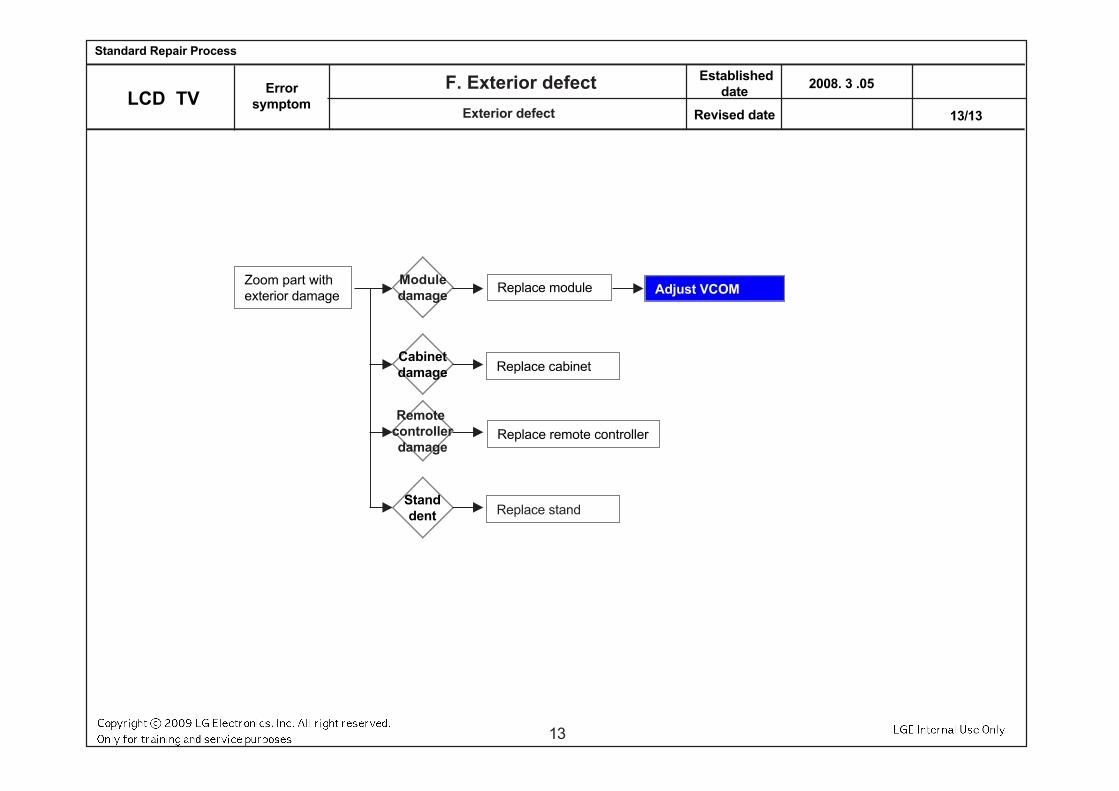
Replace moduleZoom part withexterior damage
Moduledamage
Cabinetdamage Replace cabinet
Replace remote controller
Remote controllerdamage
Standdent Replace stand
F. Exterior defect
Exterior defect
Adjust VCOM
Establisheddate
Revised date
2008. 3 .05
13/13LCD TV
Errorsymptom
Standard Repair Process
13
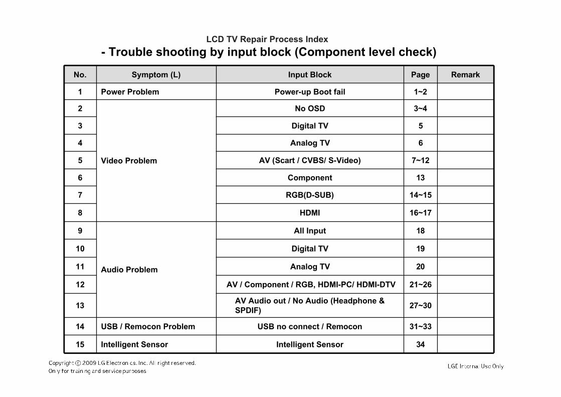
LCD TV Repair Process Index
- Trouble shooting by input block (Component level check)
No. Symptom (L) Input Block Page Remark
1 Power Problem Power-up Boot fail 1~2
2
Video Problem
No OSD 3~4
3 Digital TV 5
4 Analog TV 6
5 AV (Scart / CVBS/ S-Video) 7~12
6 Component 13
7 RGB(D-SUB) 14~15
8 HDMI 16~17
9
Audio Problem
All Input 18
10 Digital TV 19
11 Analog TV 20
12 AV / Component / RGB, HDMI-PC/ HDMI-DTV 21~26
13AV Audio out / No Audio (Headphone &SPDIF)
27~30
14 USB / Remocon Problem USB no connect / Remocon 31~33
15 Intelligent Sensor Intelligent Sensor 34
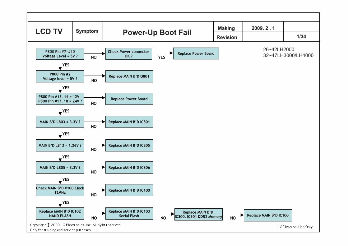
P800 Pin #7~#10Voltage Level = 5V ?
P800 Pin #2Voltage level = 5V ?
Check Power connectorOK ?
Replace Power Board
YES
NO YES
P800 Pin #13, 14 = 12V P800 Pin #17, 18 = 24V ?
NO
Replace Power Board
YES
NO
Replace MAIN B’D Q801
MAIN B’D L803 = 3.3V ? Replace MAIN B’D IC801
YES
NO
MAIN B’D L813 = 1.26V ? Replace MAIN B’D IC805
YES
NO
MAIN B’D L805 = 3.3V ? Replace MAIN B’D IC806
YES
NO
Check MAIN B’D X100 Clock12MHz Replace MAIN B’D IC100
YES
NO
Replace MAIN B’D IC102NAND FLASH
YES
Replace MAIN B’D IC103Serial FlashNO
Replace MAIN B’D IC300, IC301 DDR2 MemoryNO
Replace MAIN B’D IC100NO
Making
Revision
2009. 2 . 1
1/34 LCD TV Symptom Power-Up Boot Fail
26~42LH200032~47LH3000/LH4000
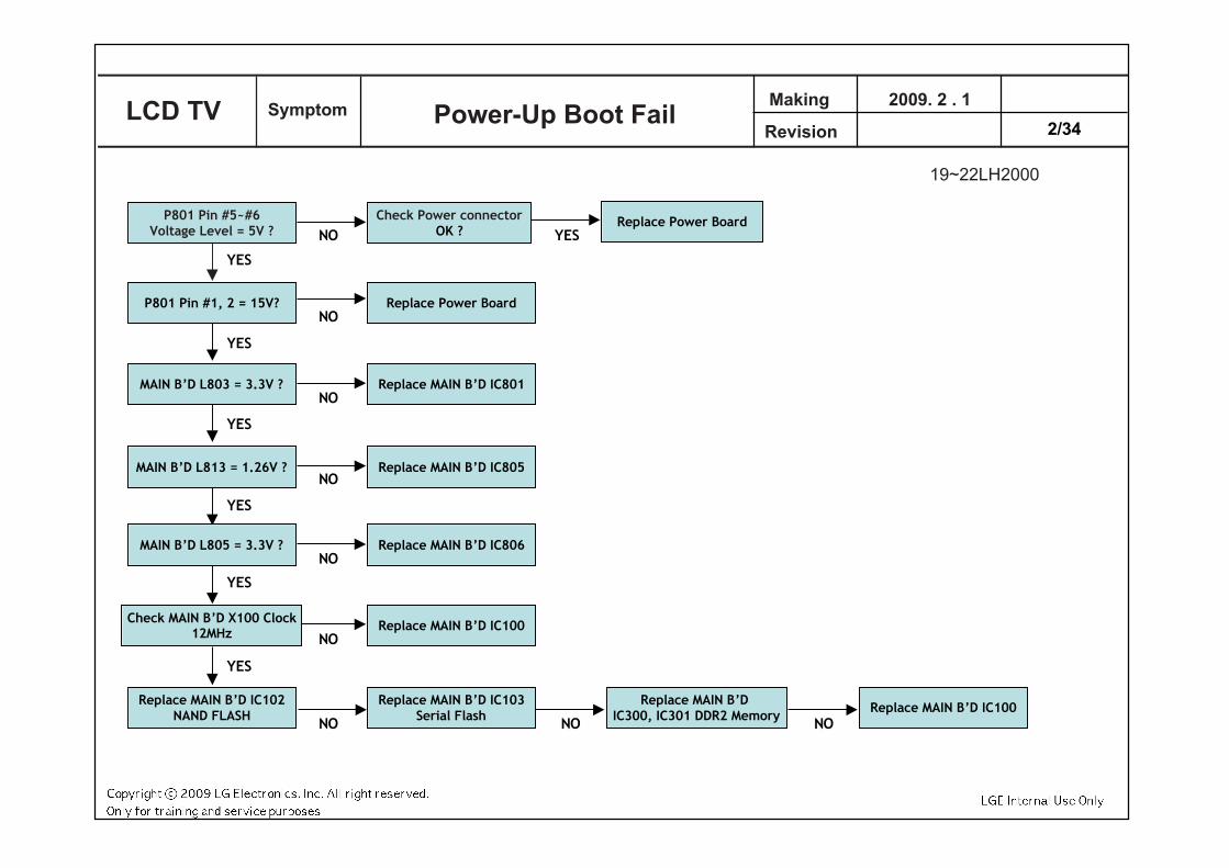
Check Power connectorOK ?
Replace Power BoardNO YES
Replace Power BoardNO
Replace MAIN B’D IC801NO
Replace MAIN B’D IC805NO
Replace MAIN B’D IC806NO
Replace MAIN B’D IC100NO
Replace MAIN B’D IC103Serial FlashNO
Replace MAIN B’D IC300, IC301 DDR2 MemoryNO
Replace MAIN B’D IC100NO
Making
Revision
2009. 2 . 1 LCD TV Symptom Power-Up Boot Fail
19~22LH2000
2/34
P801 Pin #5~#6Voltage Level = 5V ?
YES
P801 Pin #1, 2 = 15V?
MAIN B’D L803 = 3.3V ?
YES
MAIN B’D L813 = 1.26V ?
YES
MAIN B’D L805 = 3.3V ?
YES
Check MAIN B’D X100 Clock12MHz
YES
Replace MAIN B’D IC102NAND FLASH
YES
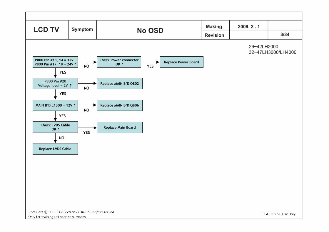
P800 Pin #20Voltage level = 2V
Check Power connectorOK ? Replace Power Board
YESNO YES
NOYES
Replace MAIN B’D Q802
MAIN B’D L1300 = 12V ? Replace MAIN B’D Q806NO
Replace Main Board
YES
P800 Pin #13, 14 = 12V P800 Pin #17, 18 = 24V ?
Check LVDS CableOK ?
YES
Replace LVDS Cable
NO
Making
Revision
2009. 2 . 1 LCD TV Symptom No OSD
26~42LH200032~47LH3000/LH4000
3/34
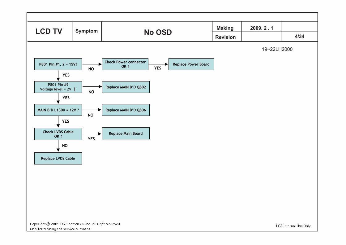
P801 Pin #9Voltage level = 2V
Check Power connectorOK ? Replace Power Board
YESNO YES
NOYES
Replace MAIN B’D Q802
MAIN B’D L1300 = 12V ? Replace MAIN B’D Q806NO
Replace Main Board
YES
P801 Pin #1, 2 = 15V?
Check LVDS CableOK ? YES
Replace LVDS Cable
NO
Making
Revision
2009. 2 . 1 LCD TV Symptom No OSD
19~22LH2000
4/34
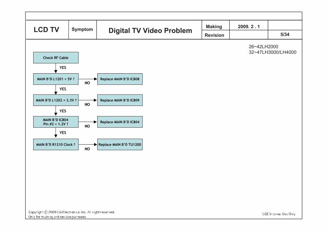
Check RF Cable
MAIN B’D L1201 = 5V ?
YES
MAIN B’D L1202 = 3.3V ?
NO
Replace MAIN B’D IC809
YES
NO
Replace MAIN B’D IC808
MAIN B’D IC804Pin #2 = 1.2V ? Replace MAIN B’D IC804
YES
NO
YES
MAIN B’D R1210 Clock ?NO
Replace MAIN B’D TU1200
Making
Revision
2009. 2 . 1 LCD TV Symptom Digital TV Video Problem
26~42LH200032~47LH3000/LH4000
5/34
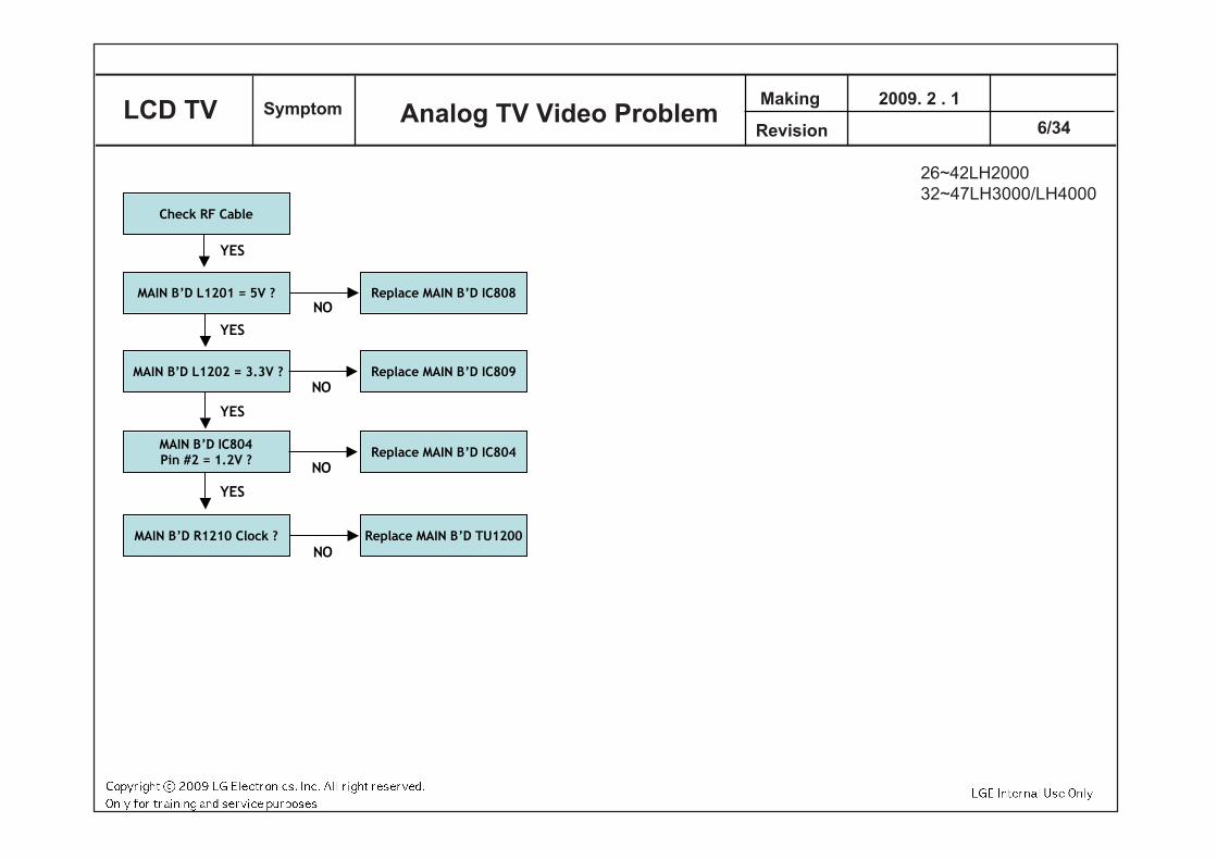
Making
Revision
2009. 2 . 1 LCD TV Symptom Analog TV Video Problem
Check RF Cable
MAIN B’D L1201 = 5V ?
YES
MAIN B’D L1202 = 3.3V ?
NO
Replace MAIN B’D IC809
YES
NO
Replace MAIN B’D IC808
MAIN B’D IC804Pin #2 = 1.2V ? Replace MAIN B’D IC804
YES
NO
YES
MAIN B’D R1210 Clock ?NO
Replace MAIN B’D TU1200
26~42LH200032~47LH3000/LH4000
6/34
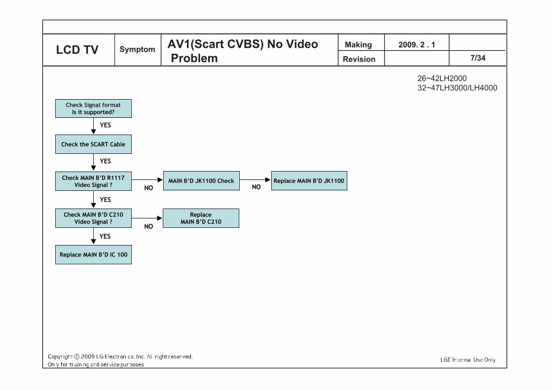
Check Signal formatIs it supported?
Check the SCART Cable
YES
MAIN B’D JK1100 Check Replace MAIN B’D JK1100
YES
NOCheck MAIN B’D R1117
Video Signal ? NO
YES
Check MAIN B’D C210Video Signal ?
ReplaceMAIN B’D C210
NO
Replace MAIN B’D IC 100
YES
Making
Revision
2009. 2 . 1 LCD TV Symptom AV1(Scart CVBS) No Video Problem
26~42LH200032~47LH3000/LH4000
7/34
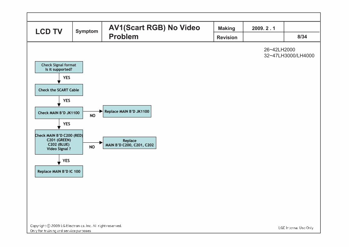
Check Signal formatIs it supported?
Check the SCART Cable
YES
Check MAIN B’D JK1100 Replace MAIN B’D JK1100
YES
NO
YES
Check MAIN B’D C200 (RED)C201 (GREEN)C202 (BLUE)Video Signal ?
ReplaceMAIN B’D C200, C201, C202NO
Replace MAIN B’D IC 100
YES
Making
Revision
2009. 2 . 1 LCD TV Symptom AV1(Scart RGB) No VideoProblem
26~42LH200032~47LH3000/LH4000
8/34
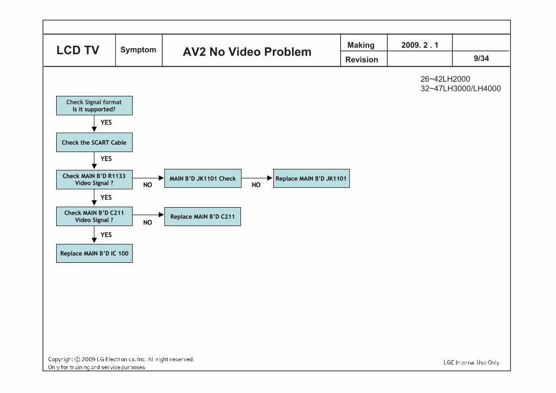
Check Signal formatIs it supported?
Check the SCART Cable
YES
MAIN B’D JK1101 Check Replace MAIN B’D JK1101
YES
NOCheck MAIN B’D R1133
Video Signal ? NO
YES
Check MAIN B’D C211Video Signal ? Replace MAIN B’D C211
NO
Replace MAIN B’D IC 100
YES
Making
Revision
2009. 2 . 1 LCD TV Symptom AV2 No Video Problem
26~42LH200032~47LH3000/LH4000
9/34
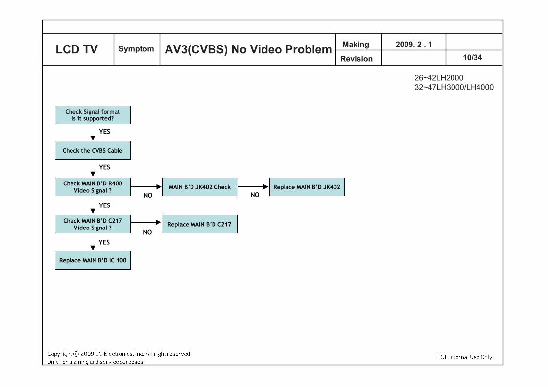
Check Signal formatIs it supported?
Check the CVBS Cable
YES
MAIN B’D JK402 Check Replace MAIN B’D JK402
YES
NO
Check MAIN B’D R400Video Signal ?
NOYES
Check MAIN B’D C217Video Signal ? Replace MAIN B’D C217
NO
Replace MAIN B’D IC 100
YES
Making
Revision
2009. 2 . 1 LCD TV Symptom AV3(CVBS) No Video Problem
26~42LH200032~47LH3000/LH4000
10/34
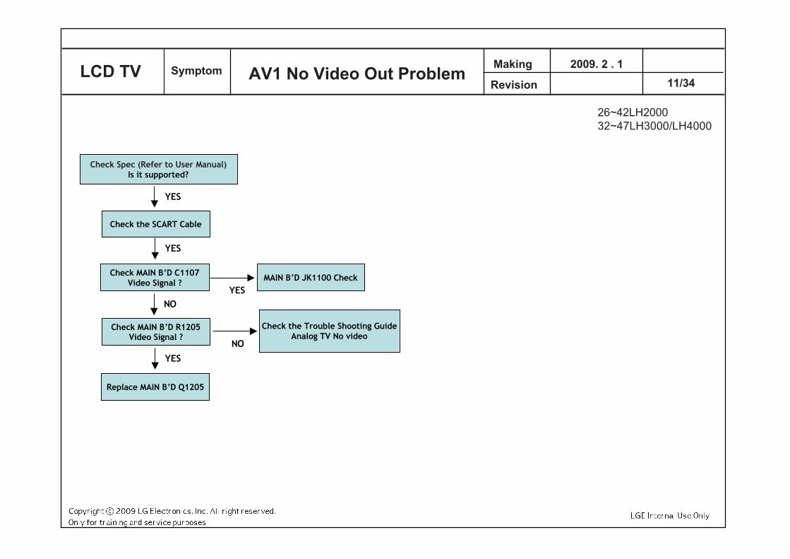
Check Spec (Refer to User Manual)Is it supported?
Check the SCART Cable
YES
Check the Trouble Shooting GuideAnalog TV No video
YES
Check MAIN B’D R1205Video Signal ?
NO
Replace MAIN B’D Q1205
YES
Check MAIN B’D C1107Video Signal ?
NO
MAIN B’D JK1100 CheckYES
Making
Revision
2009. 2 . 1
11/34 LCD TV Symptom AV1 No Video Out Problem
26~42LH200032~47LH3000/LH4000
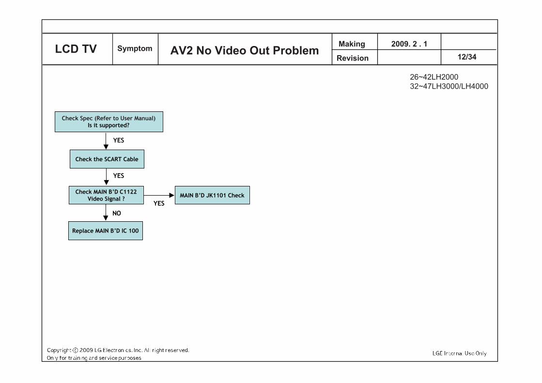
Check Spec (Refer to User Manual)Is it supported?
Check the SCART Cable
YES
YES
Check MAIN B’D C1122Video Signal ?
NO
MAIN B’D JK1101 CheckYES
Replace MAIN B’D IC 100
Making
Revision
2009. 2 . 1
12/34 LCD TV Symptom AV2 No Video Out Problem
26~42LH200032~47LH3000/LH4000
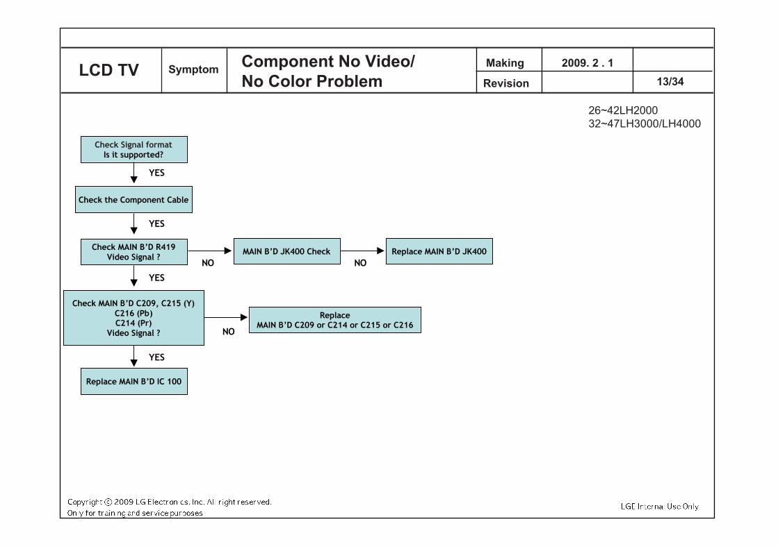
Check Signal formatIs it supported?
Check the Component Cable
YES
MAIN B’D JK400 Check Replace MAIN B’D JK400
YES
NO
Check MAIN B’D R419Video Signal ?
NO
YES
Check MAIN B’D C209, C215 (Y)C216 (Pb)C214 (Pr)
Video Signal ?
ReplaceMAIN B’D C209 or C214 or C215 or C216
NO
Replace MAIN B’D IC 100
YES
Making
Revision
2009. 2 . 1
13/34 LCD TV Symptom Component No Video/
No Color Problem
26~42LH200032~47LH3000/LH4000
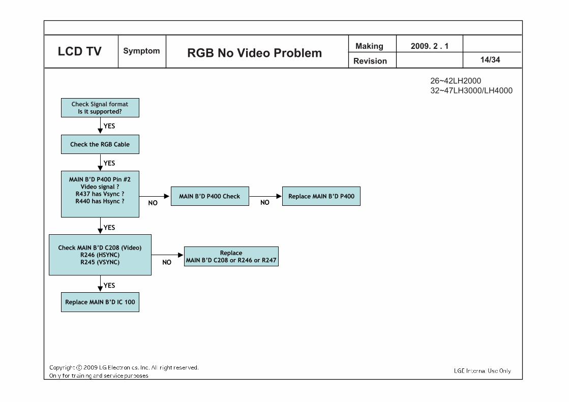
Check Signal formatIs it supported?
Check the RGB Cable
YES
MAIN B’D P400 Check Replace MAIN B’D P400
YES
NONO
YES
Check MAIN B’D C208 (Video)R246 (HSYNC)R245 (VSYNC)
ReplaceMAIN B’D C208 or R246 or R247NO
Replace MAIN B’D IC 100
YES
MAIN B’D P400 Pin #2Video signal ?
R437 has Vsync ?R440 has Hsync ?
Making
Revision
2009. 2 . 1
14/34 LCD TV Symptom RGB No Video Problem
26~42LH200032~47LH3000/LH4000
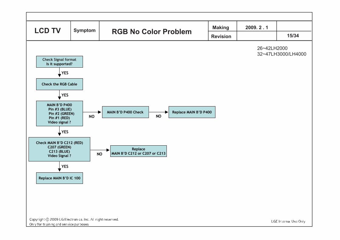
Check Signal formatIs it supported?
Check the RGB Cable
YES
MAIN B’D P400 Check Replace MAIN B’D P400
YES
NONO
YES
Check MAIN B’D C212 (RED)C207 (GREEN)C213 (BLUE)
Video Signal ?
ReplaceMAIN B’D C212 or C207 or C213NO
Replace MAIN B’D IC 100
YES
MAIN B’D P400 Pin #3 (BLUE)
Pin #2 (GREEN)Pin #1 (RED)Video signal ?
Making
Revision
2009. 2 . 1
15/34 LCD TV Symptom RGB No Color Problem
26~42LH200032~47LH3000/LH4000
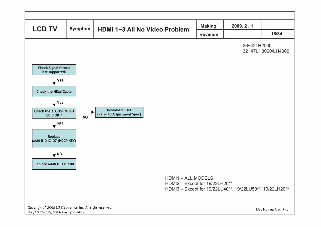
Check Signal formatIs it supported?
Check the HDMI Cable
YES
YES
Replace MAIN B’D IC 100
Check the ADJUST MENUEDID OK ?
YES
Download EDID(Refer to Adjustment Spec)
NO
NO
ReplaceMAIN B’D IC107 (HDCP KEY)
Making
Revision
2009. 2 . 1
16/34 LCD TV Symptom HDMI 1~3 All No Video Problem
HDMI1 – ALL MODELSHDMI2 – Except for 19/22LH20**HDMI3 – Except for 19/22LU40**, 19/22LU50**, 19/22LH20**
26~42LH200032~47LH3000/LH4000
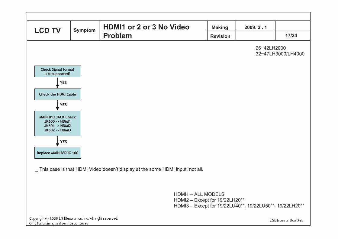
Check Signal formatIs it supported?
Check the HDMI Cable
YES
YES
Replace MAIN B’D IC 100
MAIN B’D JACK CheckJK600 -> HDMI1JK601 -> HDMI2JK602 -> HDMI3
YES
_ This case is that HDMI Video doesn’t display at the some HDMI input, not all.
Making
Revision
2009. 2 . 1
17/34 LCD TV Symptom HDMI1 or 2 or 3 No Video
Problem
HDMI1 – ALL MODELSHDMI2 – Except for 19/22LH20**HDMI3 – Except for 19/22LU40**, 19/22LU50**, 19/22LH20**
26~42LH200032~47LH3000/LH4000
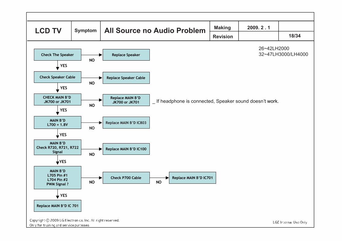
Check The Speaker
Check Speaker Cable
YES
Check P700 Cable
YES
NO
Replace MAIN B’D IC 701
YES
MAIN B’DL705 Pin #1L704 Pin #2PWM Signal ?
Replace SpeakerNO
Replace Speaker CableNO
CHECK MAIN B’D JK700 or JK701
YES
Replace MAIN B’D JK700 or JK701
NO_ If headphone is connected, Speaker sound doesn’t work.
Replace MAIN B’D IC803NO
YES
MAIN B’DL700 = 1.8V
MAIN B’DCheck R720, R721, R722
Signal
YES
Replace MAIN B’D IC100NO
Replace MAIN B’D IC701NO
Making
Revision
2009. 2 . 1
18/34 LCD TV Symptom All Source no Audio Problem
26~42LH200032~47LH3000/LH4000
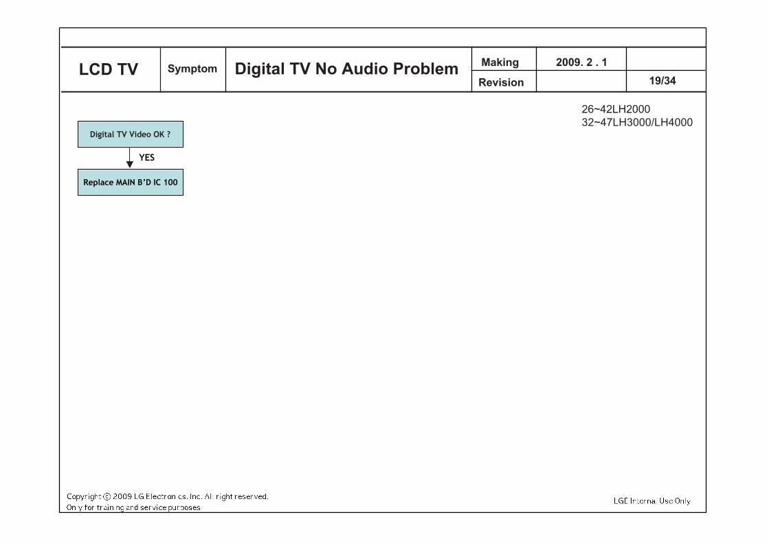
Digital TV Video OK ?
YES
Replace MAIN B’D IC 100
Making
Revision
2009. 2 . 1
19/34 LCD TV Symptom Digital TV No Audio Problem
26~42LH200032~47LH3000/LH4000
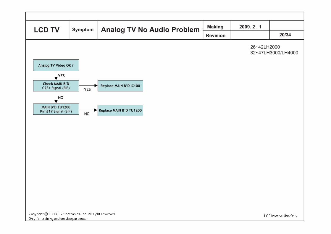
MAIN B’D TU1200Pin #17 Signal (SIF) Replace MAIN B’D TU1200
NO
Analog TV Video OK ?
YES
Check MAIN B’DC231 Signal (SIF)
NO
Replace MAIN B’D IC100YES
Making
Revision
2009. 2 . 1
20/34 LCD TV Symptom Analog TV No Audio Problem
26~42LH200032~47LH3000/LH4000

Check the SCART Cable
YES
Check MAIN B’DC229, C230
MAIN B’DC229 (Right Sound)C230 (Left Sound)
signal ? YES
NO
Replace MAIN B’D IC 100
AV1 Video OK ?
YES
Check MAIN B’D JK1100 Replace MAIN B’D JK1100NO
YES
Making
Revision
2009. 2 . 1
21/34 LCD TV Symptom AV1 No Audio Problem
26~42LH200032~47LH3000/LH4000

Check the SCART Cable
YES
Check MAIN B’DC2008, C2009
MAIN B’DC2008 (Right Sound)C2009 (Left Sound)
signal ? YES
NO
Replace MAIN B’D IC 100
AV2 Video OK ?
YES
Check MAIN B’D JK1101 Replace MAIN B’D JK1101NO
YES
Making
Revision
2009. 2 . 1
22/34 LCD TV Symptom AV2 No Audio Problem
26~42LH200032~47LH3000/LH4000
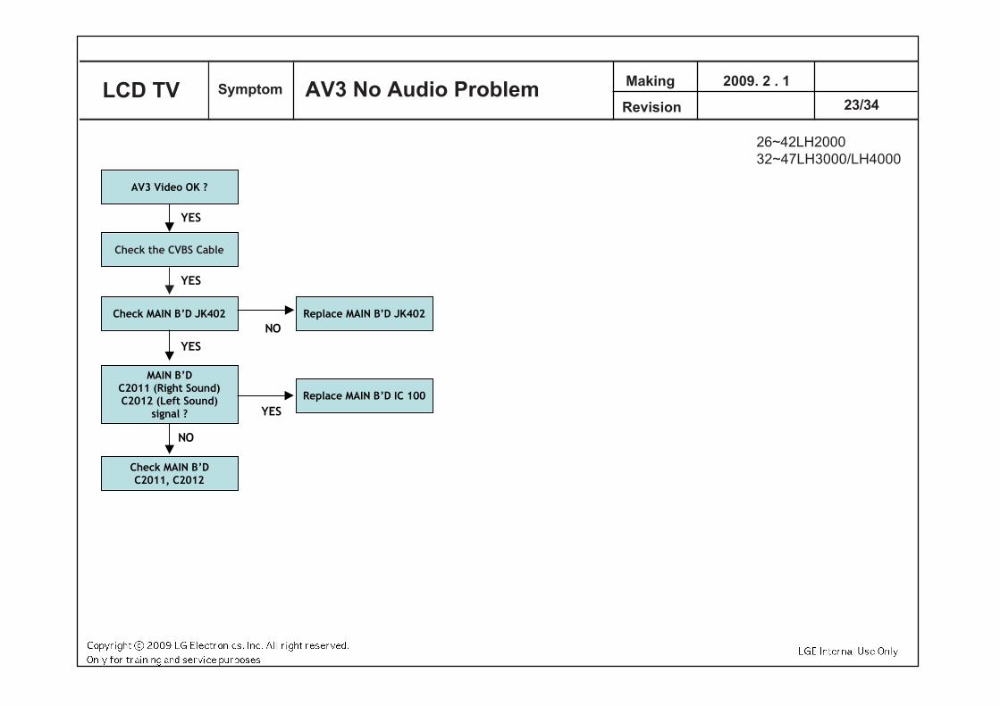
Check the CVBS Cable
YES
Check MAIN B’DC2011, C2012
MAIN B’DC2011 (Right Sound)C2012 (Left Sound)
signal ? YES
NO
Replace MAIN B’D IC 100
AV3 Video OK ?
YES
Check MAIN B’D JK402 Replace MAIN B’D JK402NO
YES
Making
Revision
2009. 2 . 1
23/34 LCD TV Symptom AV3 No Audio Problem
26~42LH200032~47LH3000/LH4000
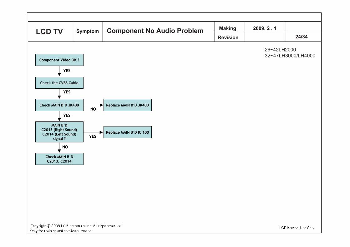
Check the CVBS Cable
YES
Check MAIN B’DC2013, C2014
MAIN B’DC2013 (Right Sound)C2014 (Left Sound)
signal ? YES
NO
Replace MAIN B’D IC 100
Component Video OK ?
YES
Check MAIN B’D JK400 Replace MAIN B’D JK400NO
YES
Making
Revision
2009. 2 . 1
24/34 LCD TV Symptom Component No Audio Problem
26~42LH200032~47LH3000/LH4000
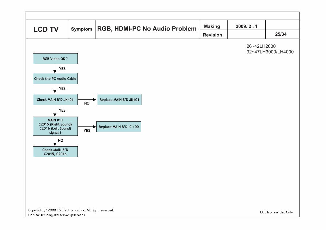
Check the PC Audio Cable
YES
Check MAIN B’DC2015, C2016
MAIN B’DC2015 (Right Sound)C2016 (Left Sound)
signal ? YES
NO
Replace MAIN B’D IC 100
RGB Video OK ?
YES
Check MAIN B’D JK401 Replace MAIN B’D JK401NO
YES
Making
Revision
2009. 2 . 1
25/34 LCD TV Symptom RGB, HDMI-PC No Audio Problem
26~42LH200032~47LH3000/LH4000
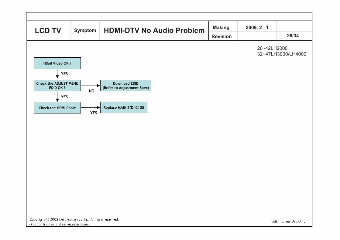
HDMI Video OK ?
YES
Check the ADJUST MENUEDID OK ?
YES
Download EDID(Refer to Adjustment Spec)
NO
Check the HDMI Cable Replace MAIN B’D IC100YES
Making
Revision
2009. 2 . 1
26/34 LCD TV Symptom HDMI-DTV No Audio Problem
26~42LH200032~47LH3000/LH4000
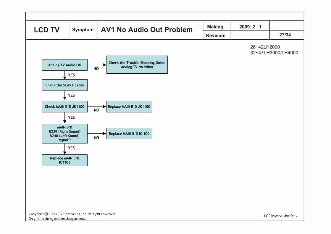
Check the SCART Cable
YES
Replace MAIN B’DIC1103
MAIN B’DR239 (Right Sound)R240 (Left Sound)
signal ? NO
YES
Replace MAIN B’D IC 100
Analog TV Audio OK
YES
Check MAIN B’D JK1100 Replace MAIN B’D JK1100NO
YES
Check the Trouble Shooting GuideAnalog TV No videoNO
Making
Revision
2009. 2 . 1
27/34 LCD TV Symptom AV1 No Audio Out Problem
26~42LH200032~47LH3000/LH4000
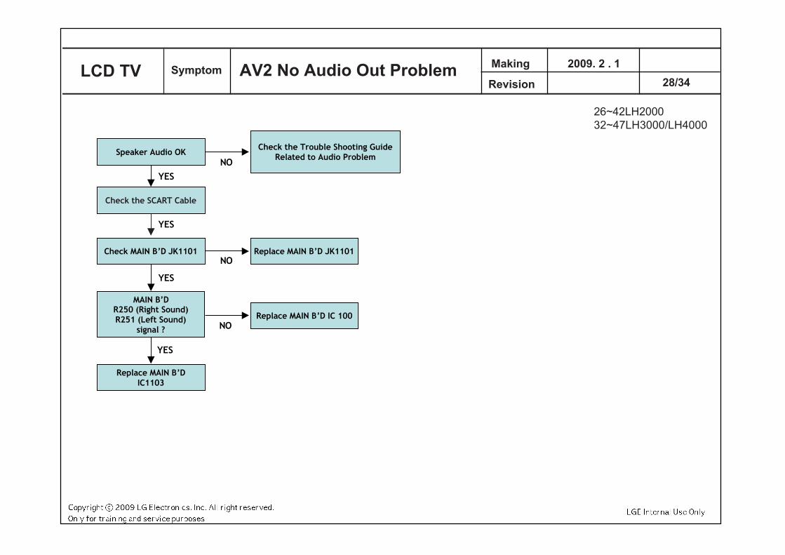
Check the SCART Cable
YES
Replace MAIN B’DIC1103
MAIN B’DR250 (Right Sound)R251 (Left Sound)
signal ? NO
YES
Replace MAIN B’D IC 100
Speaker Audio OK
YES
Check MAIN B’D JK1101 Replace MAIN B’D JK1101NO
YES
Check the Trouble Shooting GuideRelated to Audio ProblemNO
Making
Revision
2009. 2 . 1
28/34 LCD TV Symptom AV2 No Audio Out Problem
26~42LH200032~47LH3000/LH4000
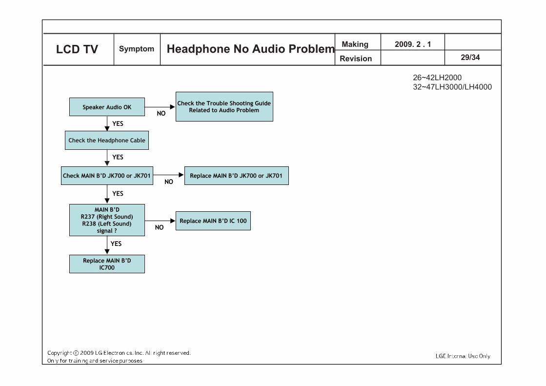
Check the Headphone Cable
YES
Replace MAIN B’DIC700
MAIN B’DR237 (Right Sound)R238 (Left Sound)
signal ? NO
YES
Replace MAIN B’D IC 100
Speaker Audio OK
YES
Check MAIN B’D JK700 or JK701 Replace MAIN B’D JK700 or JK701NO
YES
Check the Trouble Shooting GuideRelated to Audio ProblemNO
Making
Revision
2009. 2 . 1
29/34 LCD TV Symptom Headphone No Audio Problem
26~42LH200032~47LH3000/LH4000
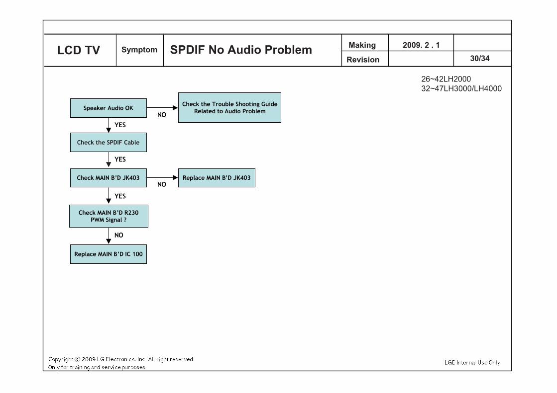
Check the SPDIF Cable
YES
Check MAIN B’D R230PWM Signal ?
Replace MAIN B’D IC 100
Speaker Audio OK
YES
Check MAIN B’D JK403 Replace MAIN B’D JK403NO
YES
NO
Check the Trouble Shooting GuideRelated to Audio ProblemNO
Making
Revision
2009. 2 . 1
30/34 LCD TV Symptom SPDIF No Audio Problem
26~42LH200032~47LH3000/LH4000
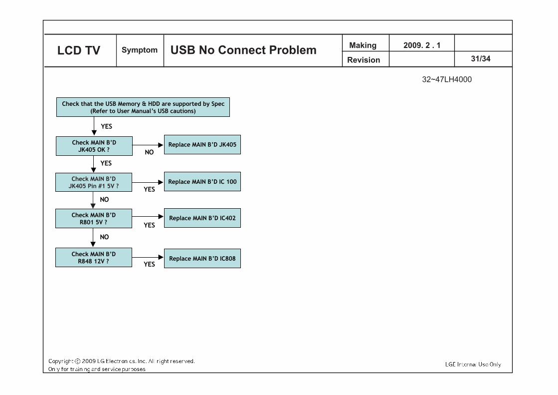
Check MAIN B’DJK405 Pin #1 5V ?
NO
Check MAIN B’DR848 12V ?
Check that the USB Memory & HDD are supported by Spec(Refer to User Manual’s USB cautions)
YES
Check MAIN B’DR801 5V ?
Replace MAIN B’D IC402YES
NO
Replace MAIN B’D IC808YES
YESReplace MAIN B’D IC 100
Check MAIN B’DJK405 OK ?
YES
NOReplace MAIN B’D JK405
Making
Revision
2009. 2 . 1
31/34 LCD TV Symptom USB No Connect Problem
32~47LH4000
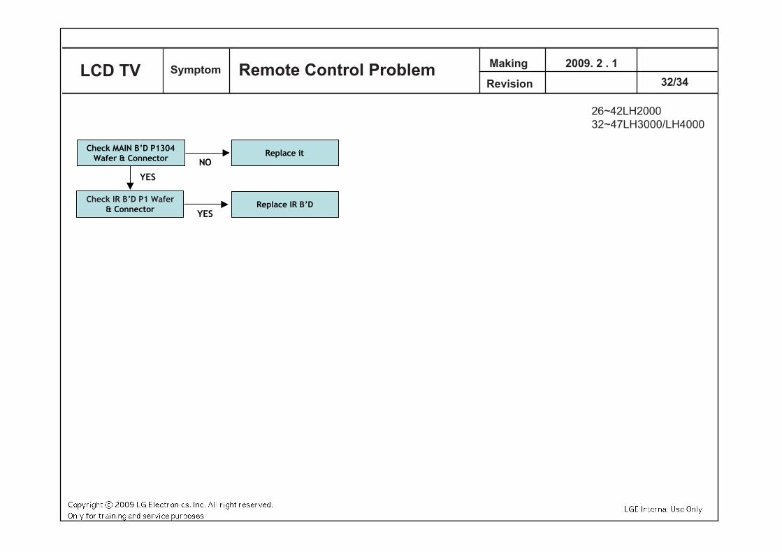
Check IR B’D P1 Wafer& Connector
Check MAIN B’D P1304Wafer & Connector
YES
NOReplace it
YESReplace IR B’D
Making
Revision
2009. 2 . 1
32/34 LCD TV Symptom Remote Control Problem
26~42LH200032~47LH3000/LH4000
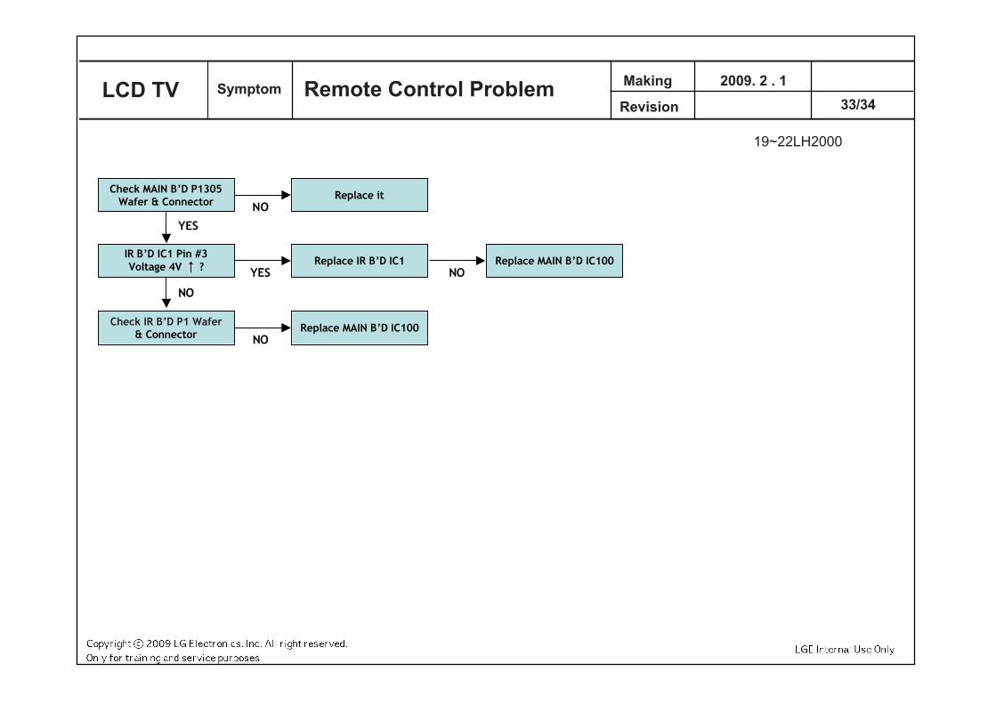
Check IR B’D P1 Wafer& Connector
Check MAIN B’D P1305Wafer & Connector
YES
NOReplace MAIN B’D IC100
IR B’D IC1 Pin #3Voltage 4V ?
NO
NOReplace it
YESReplace IR B’D IC1
NOReplace MAIN B’D IC100
Making
Revision
2009. 2 . 1
33/34 LCD TV Symptom Remote Control Problem
19~22LH2000
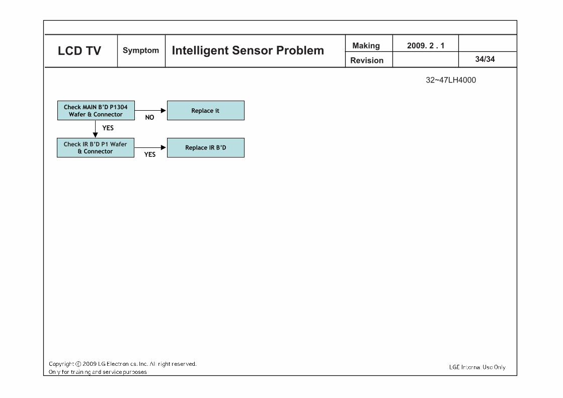
Check IR B’D P1 Wafer& Connector
Check MAIN B’D P1304Wafer & Connector
YES
YES
NOReplace it
Replace IR B’D
Making
Revision
2009. 2 . 1
34/34 LCD TV Symptom Intelligent Sensor Problem
32~47LH4000