Embed Size (px)
Citation preview
LE CG P3A 01
1 Version 1.3 | 2019-09-05
Produktdatenblatt | Version 1.1 www.osram-os.com
Applications
LE CG P3A 01
OSRAM OSTAR® Projection PowerOSRAM OSTAR Projection Power is a high lumi-nance LED for projection applications.
— Projection Home LED & Laser — Projection Professional LED & Laser
Features: — Package: OSTAR High Power Projection
— Chip technology: UX:3
— Typ. Radiation: 120° (Lambertian emitter)
— Color: Cx = 0.318, Cy = 0.642 acc. to CIE 1931 (● converted green)
— Corrosion Robustness Class: 3B
— ESD: 2 kV acc. to ANSI/ESDA/JEDEC JS-001 (HBM, Class 2)
Ordering Information
Type Luminous Flux 1) Ordering CodeIF = 36000 mAΦV
LE CG P3A 01-6V6W-1 8000 ... 14000 lm Q65112A3032
LE CG P3A 01
2 Version 1.3 | 2019-09-05
Maximum RatingsParameter Symbol Values
Operating Temperature Top min. max.
-40 °C125 °C
Storage Temperature Tstg min. max.
-40 °C125 °C
Junction Temperature Tj max. 150 °C
Forward Current TJ = 150 °C; all chips operated in parallel
IF min. max.
600 mA30000 mA
Forward Current pulsed D = 0.5 ; TB = 25 °C; all chips operated in parallel
IF pulse 48000 mA
Surge Current tp ≤ 10 μs; D = 0.1; TJ = 150 °C; all chips operated in parallel
IFS max. 60000 mA
ESD withstand voltage acc. to ANSI/ESDA/JEDEC JS-001 (HBM, Class 2)
VESD 2 kV
Reverse current 2) IR max. 200 mA
LE CG P3A 01
3 Version 1.3 | 2019-09-05
CharacteristicsTBoard = 25 °C; IF = 36000 mA; f = 1000 Hz; tint = 100 ms; D = 0.5; all chips operated in parallel
Parameter Symbol Values
Chromaticity Coordinate 3) within λ = 500 ... 600 nm
Cx Cy
typ. typ.
0.3180.642
Peak Wavelength λpeak typ. 520 nm
Spectral bandwidth at 50% Irel,max ∆λ typ. 100 nm
Viewing angle at 50% IV 2φ typ. 120 °
Radiating surface Acolor typ. 4.8 x 2.6 mm²
Partial Flux acc. CIE 127:2007 4) IF = 36000 mA
ΦE/V, 120° typ. 0.77
Forward Voltage 5) IF = 36000 mA; all chips operated in parallel
VF min. typ. max.
3.20 V3.35 V4.30 V
Deviation of forward voltage of all chips VF max. 135 mV
Reverse voltage (ESD device) VR ESD min. 45 V
Reverse voltage 2) IR = 20 mA
VR max. 1.2 V
Real thermal resistance junction/board 6) RthJB real typ. 0.5
Electrical thermal resistance junction/board 6) with efficiency ηe = 18 %
RthJB elec. typ. 0.41
Brightness Groups
Group Luminous Flux 1) Luminous Flux 1)
IF = 36000 mA IF = 36000 mAmin. max.ΦV ΦV
6V 8000 lm 9000 lm
7V 9000 lm 10000 lm
8V 10000 lm 11200 lm
5W 11200 lm 12500 lm
6W 12500 lm 14000 lm
LE CG P3A 01
4 Version 1.3 | 2019-09-05
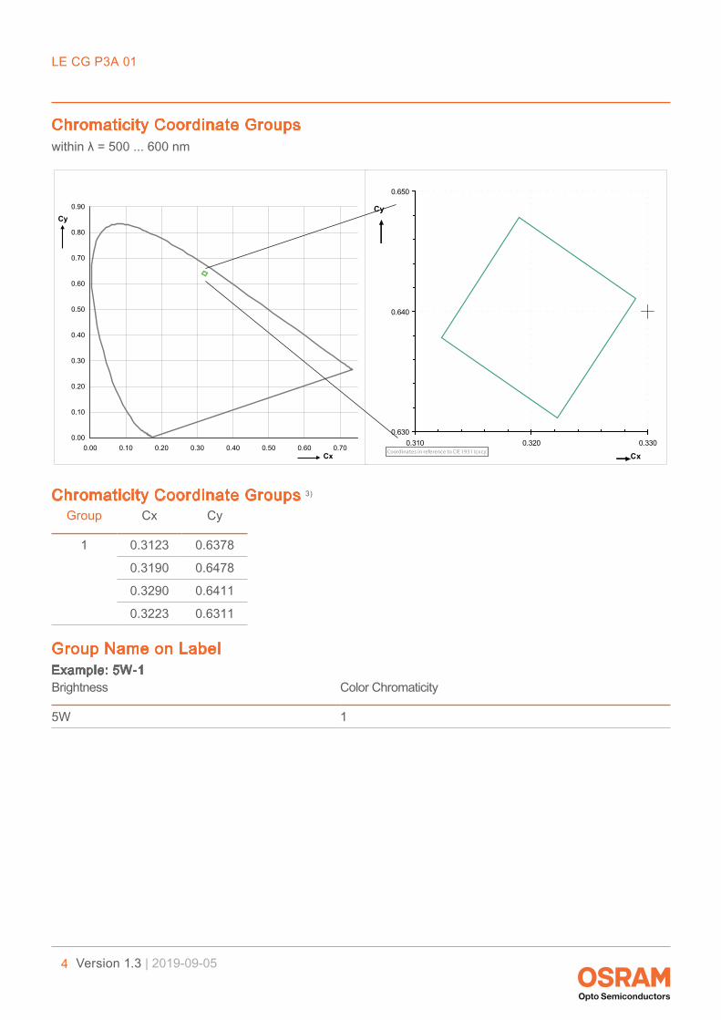
Chromaticity Coordinate Groupswithin λ = 500 ... 600 nm
0.00
0.10
0.20
0.30
0.40
0.50
0.60
0.70
0.80
0.90
0.00 0.10 0.20 0.30 0.40 0.50 0.60 0.70Cx
Cy
0.630
0.640
0.650
0.310 0.320 0.330
Cx
Cy
Coordinates in reference to CIE 1931 (cx cy)
Chromaticity Coordinate Groups 3)
Group Cx Cy
1 0.3123 0.6378
0.3190 0.6478
0.3290 0.6411
0.3223 0.6311
Group Name on Label Example: 5W-1Brightness Color Chromaticity
5W 1
LE CG P3A 01
5 Version 1.3 | 2019-09-05
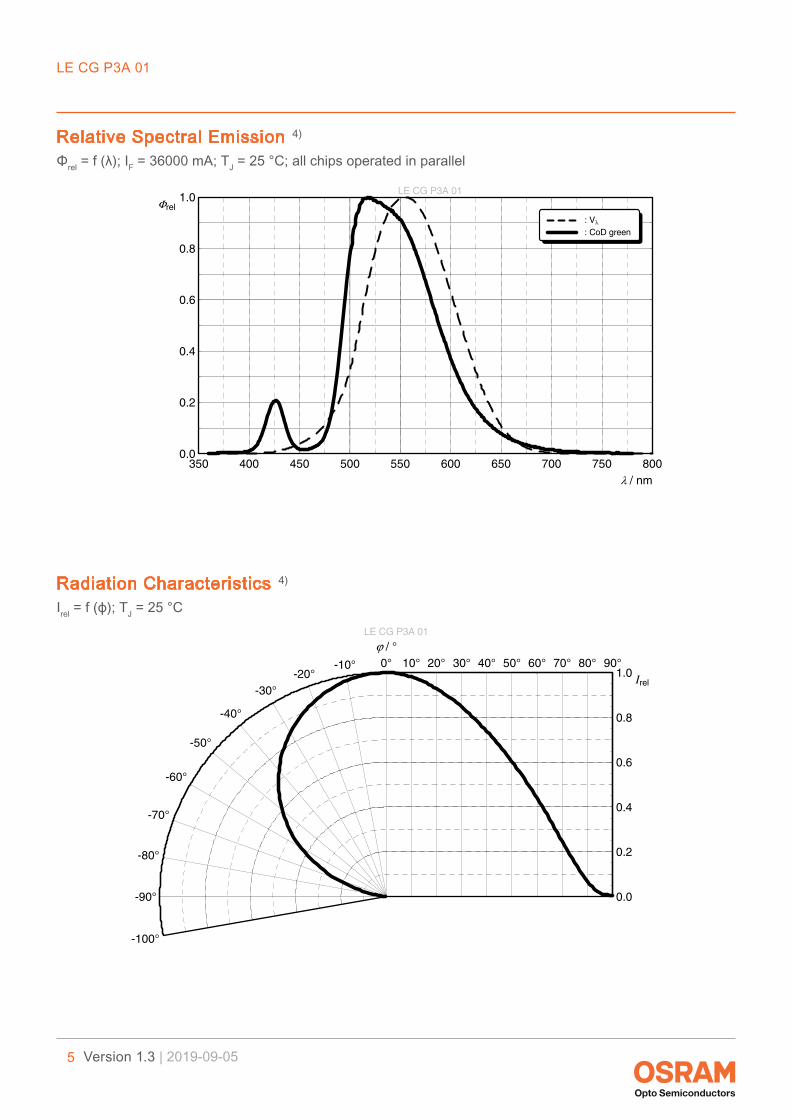
Relative Spectral Emission 4)
Φrel = f (λ); IF = 36000 mA; TJ = 25 °C; all chips operated in parallel
LE CG P3A 01
350 400 450 500 550 600 650 700 750 800λ / nm
0.0
0.2
0.4
0.6
0.8
1.0Φrel
: Vλ
: CoD green
Radiation Characteristics 4)
Irel = f (ϕ); TJ = 25 °CLE CG P3A 01
-100°
-90°
-80°
-70°
-60°
-50°
-40°
-30°-20°
-10° 0° 10° 20° 30° 40° 50° 60° 70° 80° 90°ϕ / °
0.0
0.2
0.4
0.6
0.8
1.0Irel
LE CG P3A 01
6 Version 1.3 | 2019-09-05
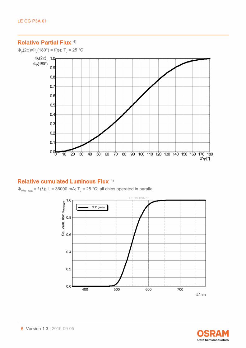
Relative Partial Flux 4)
ΦV(2φ)/ΦV(180°) = f(φ); TJ = 25 °C
0 10 20 30 40 50 60 70 80 90 100 110 120 130 140 150 160 170 1802*ϕ [°]
0.0
0.1
0.2
0.3
0.4
0.5
0.6
0.7
0.8
0.9
1.0ΦV(2ϕ)ΦV(180°)
Relative cumulated Luminous Flux 4)
ΦVrel - cum = f (λ); IF = 36000 mA; TJ = 25 °C; all chips operated in parallel
LE CG P3A 01
400 500 600 700λ / nm
0.0
0.2
0.4
0.6
0.8
1.0
Rel
.cum
.flu
xΦ
Vre
lcum
: CoD green
LE CG P3A 01
7 Version 1.3 | 2019-09-05
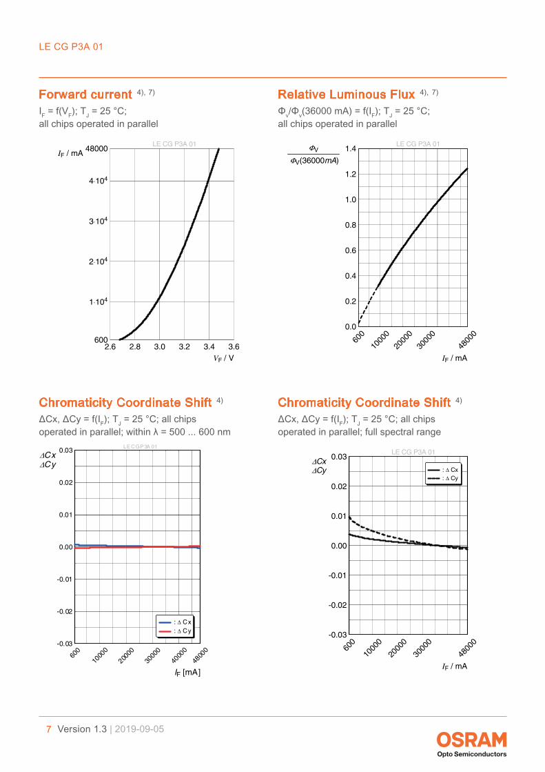
Forward current 4), 7)
IF = f(VF); TJ = 25 °C; all chips operated in parallel
LE CG P3A 01
2.6 2.8 3.0 3.2 3.4 3.6VF / V
600
48000
1⋅104
2⋅104
3⋅104
4⋅104
IF / mA
Relative Luminous Flux 4), 7)
Φv/Φv(36000 mA) = f(IF); TJ = 25 °C; all chips operated in parallel
LE CG P3A 01
600
4800
0
1000
0
2000
0
3000
0
IF / mA
0.0
0.2
0.4
0.6
0.8
1.0
1.2
1.4ΦV
ΦV(36000mA)
Chromaticity Coordinate Shift 4)
ΔCx, ΔCy = f(IF); TJ = 25 °C; all chips operated in parallel; within λ = 500 ... 600 nm
LE CG P3A 01
600
4800
0
1000
0
20000
3000
0
4000
0
IF [mA]
-0.03
-0.02
-0.01
0.00
0.01
0.02
0.03∆Cx∆Cy
: ∆ Cx: ∆ Cy
Chromaticity Coordinate Shift 4)
ΔCx, ΔCy = f(IF); TJ = 25 °C; all chips operated in parallel; full spectral range
LE CG P3A 01
600
4800
0
1000
0
2000
0
3000
0
IF / mA
-0.03
-0.02
-0.01
0.00
0.01
0.02
0.03∆Cx∆Cy : ∆ Cx
: ∆ Cy
LE CG P3A 01
8 Version 1.3 | 2019-09-05
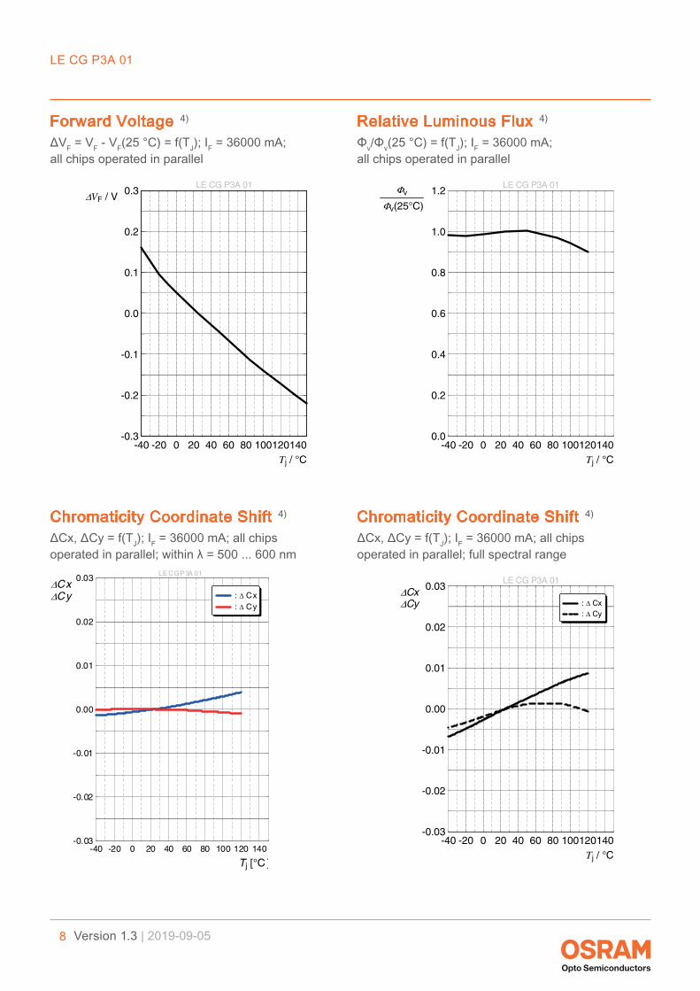
Forward Voltage 4)
ΔVF = VF - VF(25 °C) = f(TJ); IF = 36000 mA; all chips operated in parallel
LE CG P3A 01
-40 -20 0 20 40 60 80 100120140Tj / °C
-0.3
-0.2
-0.1
0.0
0.1
0.2
0.3∆VF / V
Relative Luminous Flux 4)
Φv/Φv(25 °C) = f(TJ); IF = 36000 mA; all chips operated in parallel
LE CG P3A 01
-40 -20 0 20 40 60 80 100120140Tj / °C
0.0
0.2
0.4
0.6
0.8
1.0
1.2Φv
Φv(25°C)
Chromaticity Coordinate Shift 4)
ΔCx, ΔCy = f(TJ); IF = 36000 mA; all chips operated in parallel; within λ = 500 ... 600 nm
LE CG P3A 01
-40 -20 0 20 40 60 80 100 120 140
Tj [°C ]
-0.03
-0.02
-0.01
0.00
0.01
0.02
0.03∆Cx∆Cy : ∆ Cx
: ∆ Cy
Chromaticity Coordinate Shift 4)
ΔCx, ΔCy = f(TJ); IF = 36000 mA; all chips operated in parallel; full spectral range
LE CG P3A 01
-40 -20 0 20 40 60 80 100120140Tj / °C
-0.03
-0.02
-0.01
0.00
0.01
0.02
0.03∆Cx∆Cy : ∆ Cx
: ∆ Cy
LE CG P3A 01
9 Version 1.3 | 2019-09-05
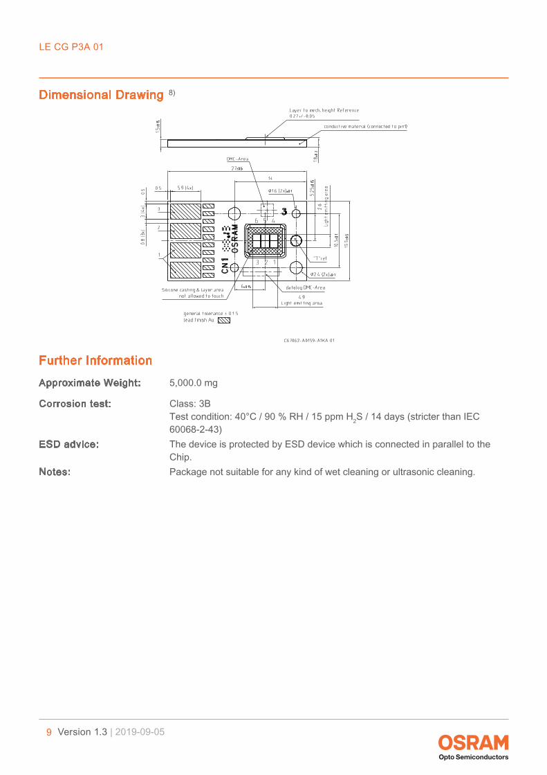
Dimensional Drawing 8)
Further Information
Approximate Weight: 5,000.0 mg
Corrosion test: Class: 3B Test condition: 40°C / 90 % RH / 15 ppm H2S / 14 days (stricter than IEC 60068-2-43)
ESD advice: The device is protected by ESD device which is connected in parallel to the Chip.
Notes: Package not suitable for any kind of wet cleaning or ultrasonic cleaning.
LE CG P3A 01
10 Version 1.3 | 2019-09-05
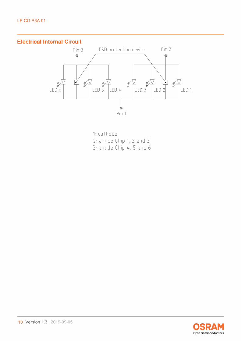
Electrical Internal Circuit
LE CG P3A 01
11 Version 1.3 | 2019-09-05
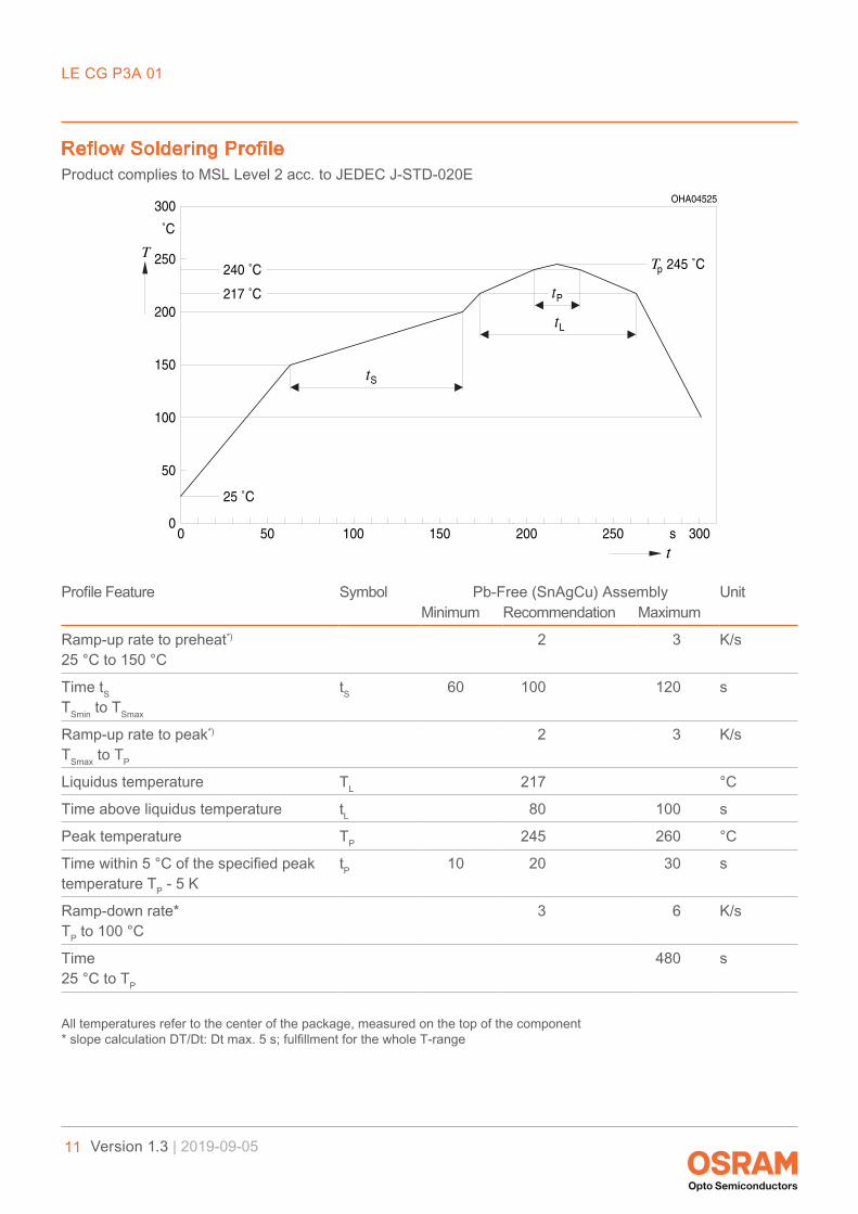
Reflow Soldering ProfileProduct complies to MSL Level 2 acc. to JEDEC J-STD-020E
00
s
OHA04525
50
100
150
200
250
300
50 100 150 200 250 300t
T
˚C
St
t
Pt
Tp240 ˚C
217 ˚C
245 ˚C
25 ˚C
L
Profile Feature Symbol Pb-Free (SnAgCu) Assembly UnitMinimum Recommendation Maximum
Ramp-up rate to preheat*)
25 °C to 150 °C2 3 K/s
Time tSTSmin to TSmax
tS 60 100 120 s
Ramp-up rate to peak*)
TSmax to TP
2 3 K/s
Liquidus temperature TL 217 °C
Time above liquidus temperature tL 80 100 s
Peak temperature TP 245 260 °C
Time within 5 °C of the specified peaktemperature TP - 5 K
tP 10 20 30 s
Ramp-down rate*TP to 100 °C
3 6 K/s
Time25 °C to TP
480 s
All temperatures refer to the center of the package, measured on the top of the component* slope calculation DT/Dt: Dt max. 5 s; fulfillment for the whole T-range
LE CG P3A 01
12 Version 1.3 | 2019-09-05
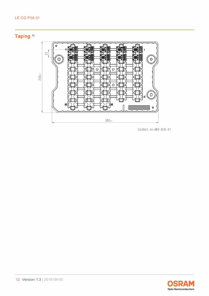
Taping 8)
LE CG P3A 01
13 Version 1.3 | 2019-09-05
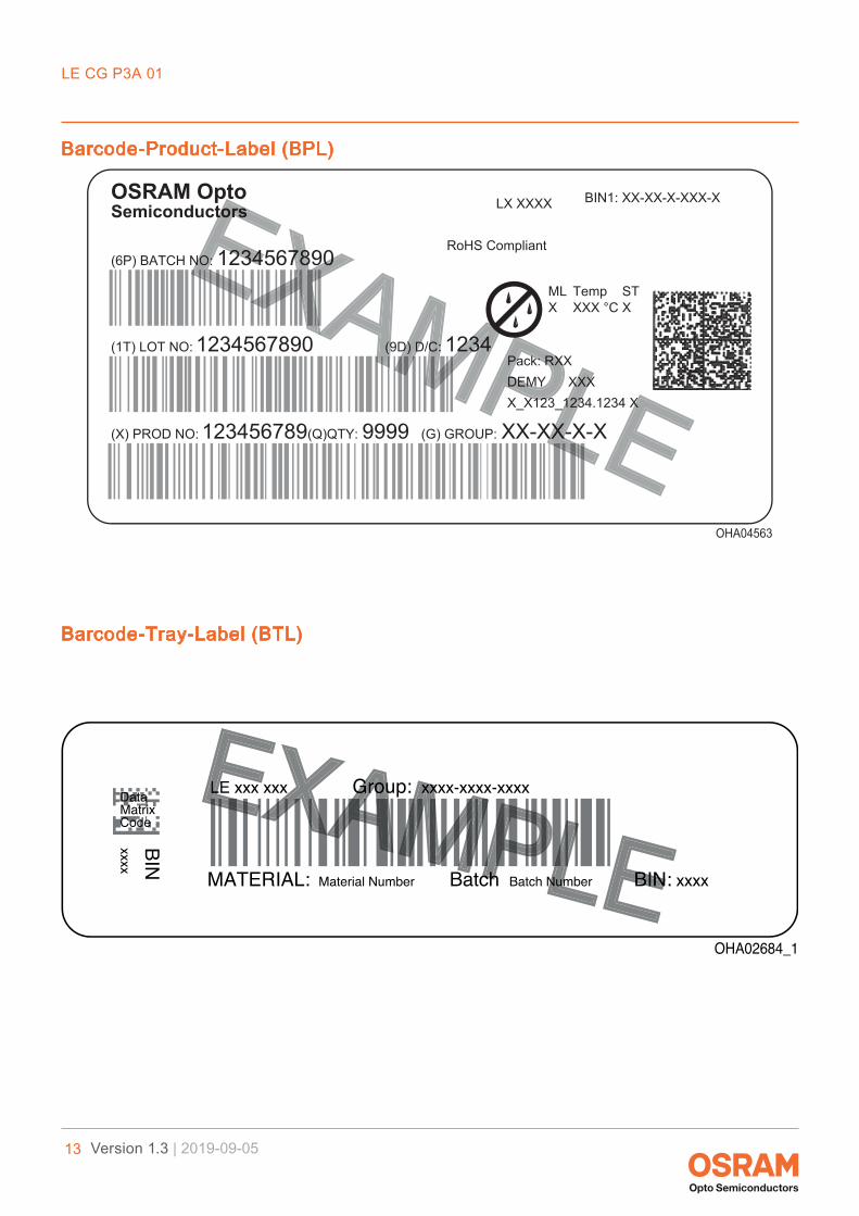
Barcode-Product-Label (BPL)
Barcode-Tray-Label (BTL)
LE CG P3A 01
14 Version 1.3 | 2019-09-05
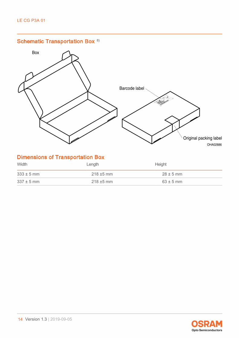
Schematic Transportation Box 8)
OHA02886
PACKVAR:
R077Additional TEXT
P-1+Q-1
Multi TOPLED
Muste
r
OSRAM Opto
Semiconductors
(6P) BATCH NO:
(X) PROD NO:
10
(9D) D/C:
11(1T) LOT NO:
210021998
123GH1234
024 5
(Q)QTY: 2000
0144
(G) GROUP:
260 C RT240 C R
3
220 C R
MLBin3:Bin2: Q
-1-20
Bin1: P-1-20
LSY T6762
2a
Temp ST
R18DEMY
Barcode label
Original packing label
Box
Dimensions of Transportation BoxWidth Length Height
333 ± 5 mm 218 ±5 mm 28 ± 5 mm
337 ± 5 mm 218 ±5 mm 63 ± 5 mm
LE CG P3A 01
15 Version 1.3 | 2019-09-05
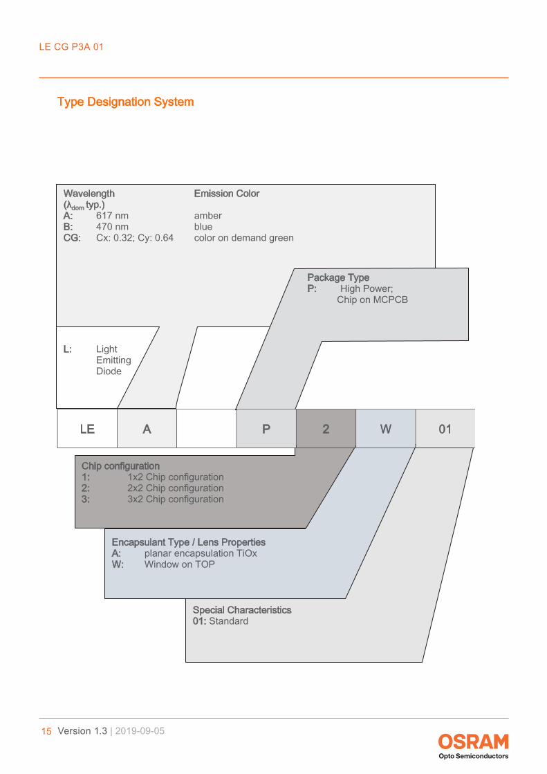
Special Characteristics 01: Standard
Encapsulant Type / Lens Properties A: planar encapsulation TiOx W: Window on TOP
Wavelength Emission Color (λdom typ.) A: 617 nm amber B: 470 nm blue CG: Cx: 0.32; Cy: 0.64 color on demand green
L: Light Emitting Diode
Package Type P: High Power; Chip on MCPCB
Chip configuration 1: 1x2 Chip configuration 2: 2x2 Chip configuration 3: 3x2 Chip configuration
Type Designation System
LE A P 2 W 01
LE CG P3A 01
16 Version 1.3 | 2019-09-05
Data Matrix Code Description
The Data Matrix Code bin information is Laser marked during testing
Content: aaaa@bbbb@ccc@ddddd@eeeee
Data Matrix Code Type: ECC200
a = Luminous Flux (Phiv) [lm] or Radiant Flux (Phie) [W] (example: 3306)
b = Forward Voltage (Vf) [V] (example: 3.46)
c = Wavelength (Ldom) [nm] (example: 618)
d = Color Coordinate Cx (example: 0.321)
e = Color Coordinate Cy (example: 0.641)
@: Seperator = Blank
LE CG P3A 01
17 Version 1.3 | 2019-09-05
NotesThe evaluation of eye safety occurs according to the standard IEC 62471:2006 (photo biological safety of lamps and lamp systems). Within the risk grouping system of this IEC standard, the device specified in this data sheet falls into the class moderate risk (exposure time 0.25 s). Under real circumstances (for exposure time, conditions of the eye pupils, observation distance), it is assumed that no endangerment to the eye ex-ists from these devices. As a matter of principle, however, it should be mentioned that intense light sources have a high secondary exposure potential due to their blinding effect. When looking at bright light sources (e.g. headlights), temporary reduction in visual acuity and afterimages can occur, leading to irritation, annoy-ance, visual impairment, and even accidents, depending on the situation.
Subcomponents of this device contain, in addition to other substances, metal filled materials including silver. Metal filled materials can be affected by environments that contain traces of aggressive substances. There-fore, we recommend that customers minimize device exposure to aggressive substances during storage, production, and use. Devices that showed visible discoloration when tested using the described tests above did show no performance deviations within failure limits during the stated test duration. Respective failure limits are described in the IEC60810.
For further application related information please visit www.osram-os.com/appnotes
LE CG P3A 01
18 Version 1.3 | 2019-09-05
Disclaimer
Attention please!The information describes the type of component and shall not be considered as assured characteristics.Terms of delivery and rights to change design reserved. Due to technical requirements components may contain dangerous substances.For information on the types in question please contact our Sales Organization.If printed or downloaded, please find the latest version on the OSRAM OS website.
PackingPlease use the recycling operators known to you. We can also help you – get in touch with your nearest sales office. By agreement we will take packing material back, if it is sorted. You must bear the costs of transport. For packing material that is returned to us unsorted or which we are not obliged to accept, we shall have to invoice you for any costs incurred.
Product and functional safety devices/applications or medical devices/applicationsOSRAM OS components are not developed, constructed or tested for the application as safety relevant component or for the application in medical devices.OSRAM OS products are not qualified at module and system level for such application.
In case buyer – or customer supplied by buyer – considers using OSRAM OS components in product safety devices/applications or medical devices/applications, buyer and/or customer has to inform the local sales partner of OSRAM OS immediately and OSRAM OS and buyer and /or customer will analyze and coordi-nate the customer-specific request between OSRAM OS and buyer and/or customer.
LE CG P3A 01
19 Version 1.3 | 2019-09-05
Glossary1) Brightness: Brightness values are measured during a pulse train of 100 ms with a pulse width of 500
µs and a frequencey of 1 kHz, with an internal reproducibility of +/‐ 8 % and an expanded uncertainty of +/‐ 11 % (acc. to GUM with a coverage factor of k = 3). The peak brightness is calculated according to the pulse duration and frequency.
2) Reverse Operation: Reverse Operation of 10 hours is permissible in total. Continuous reverse opera-tion is not allowed.
3) Chromaticity coordinate groups: Chromaticity coordinates are measured during a pulse train of 100 ms with a pulse width of 500 µs and a frequencey of 1 kHz , with an internal reproducibility of +/‐ 0,005 and an expanded uncertainty of +/‐ 0,01 (acc. to GUM with a coverage factor of k = 3).
4) Typical Values: Due to the special conditions of the manufacturing processes of semiconductor devic-es, the typical data or calculated correlations of technical parameters can only reflect statistical figures. These do not necessarily correspond to the actual parameters of each single product, which could dif-fer from the typical data and calculated correlations or the typical characteristic line. If requested, e.g. because of technical improvements, these typ. data will be changed without any further notice.
5) Forward Voltage: The forward voltage is measured during a pulse of typical 500 µs, with an internal reproducibility of +/‐ 0,05 V and an expanded uncertainty of +/‐ 0,1 V (acc. to GUM with a coverage factor of k=3).
6) Thermal Resistance: Rth max is based on statistic values (6σ).7) Characteristic curve: In the range where the line of the graph is broken, you must expect higher differ-
ences between single devices within one packing unit.8) Tolerance of Measure: Unless otherwise noted in drawing, tolerances are specified with ±0.1 and
dimensions are specified in mm.
LE CG P3A 01
20 Version 1.3 | 2019-09-05
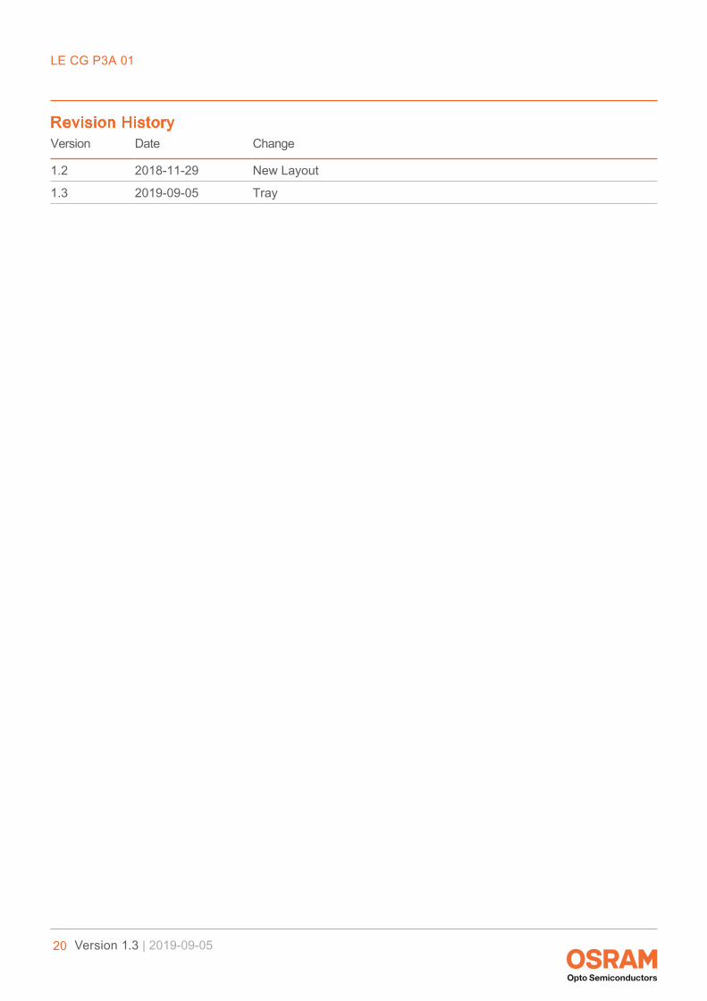
Revision HistoryVersion Date Change
1.2 2018-11-29 New Layout
1.3 2019-09-05 Tray
LE CG P3A 01
21 Version 1.3 | 2019-09-05
Published by OSRAM Opto Semiconductors GmbH Leibnizstraße 4, D-93055 Regensburg www.osram-os.com © All Rights Reserved.