Embed Size (px)
Citation preview
Lecture 19: Case Study: An Implementation of Cortex-M3 – the LM3S9B96

Stellaris® LM3S9B96 MicrocontrollerData Sheet
Chapter 1Architectural Overview
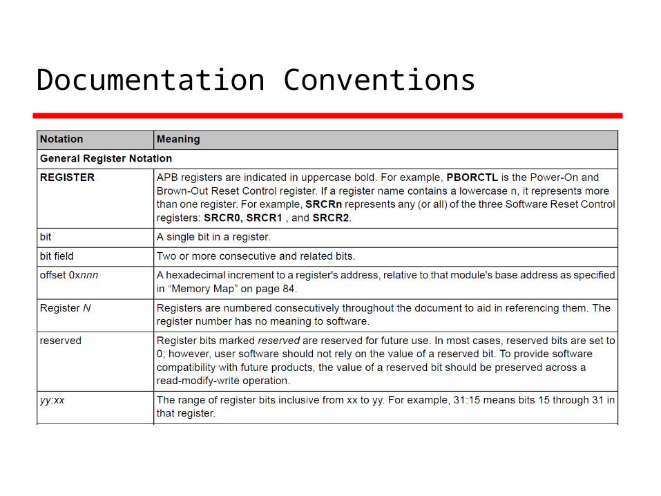
Documentation Conventions
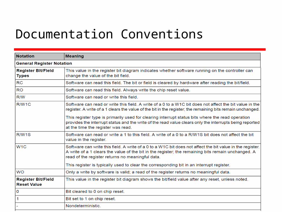
Documentation Conventions
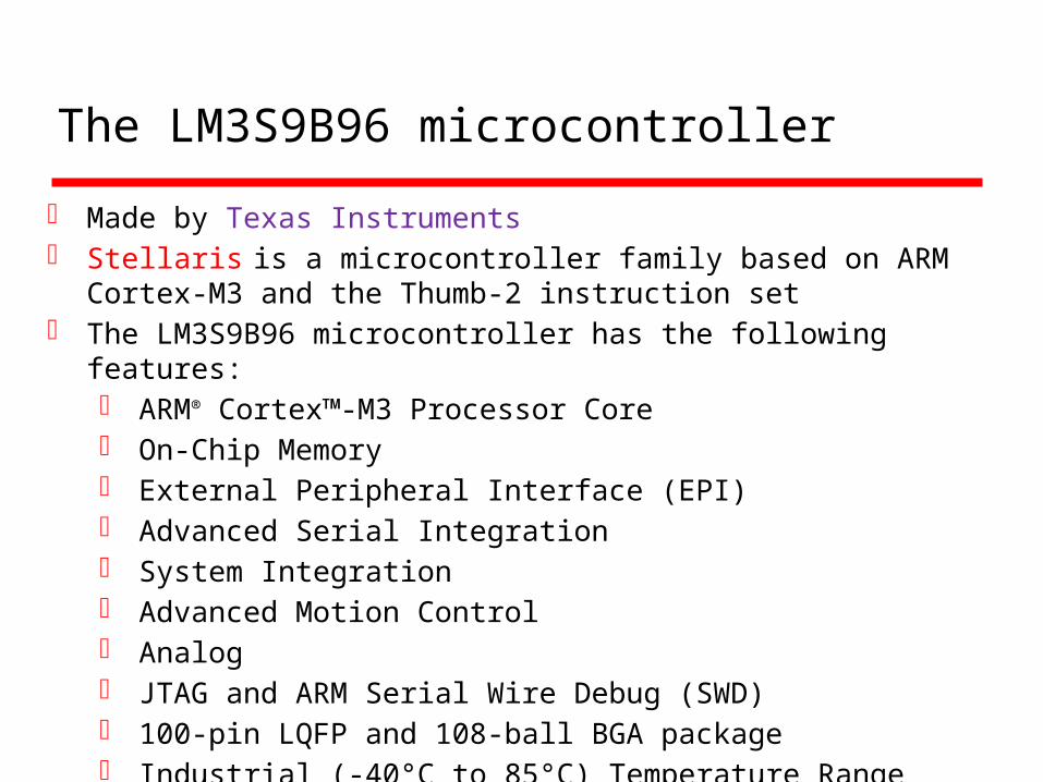
The LM3S9B96 microcontroller
Made by Texas Instruments Stellaris is a microcontroller family based on ARM Cortex-M3
and the Thumb-2 instruction set The LM3S9B96 microcontroller has the following features:
ARM® Cortex™-M3 Processor Core On-Chip Memory External Peripheral Interface (EPI) Advanced Serial Integration System Integration Advanced Motion Control Analog JTAG and ARM Serial Wire Debug (SWD) 100-pin LQFP and 108-ball BGA package Industrial (-40°C to 85°C) Temperature Range

ARM Cortex™-M3
Processor Core 32-bit ARM® Cortex™-M3 v7M architecture Outstanding processing performance combined with fast
interrupt handling Thumb-2 mixed 16-/32-bit instruction set: high performance in
a compact memory size Single-cycle multiply instruction and hardware divide
operation Atomic bit manipulation (bit-banding) Unaligned data access
Harvard architecture: separate buses for instruction and data Deterministic, high-performance interrupt handling for time-
critical apps. Enhanced system debug with extensive breakpoint and trace
capabilities Ultra-low power consumption with integrated sleep modes 80-MHz operation, 100 DMIPS performance
ARM Cortex™-M3
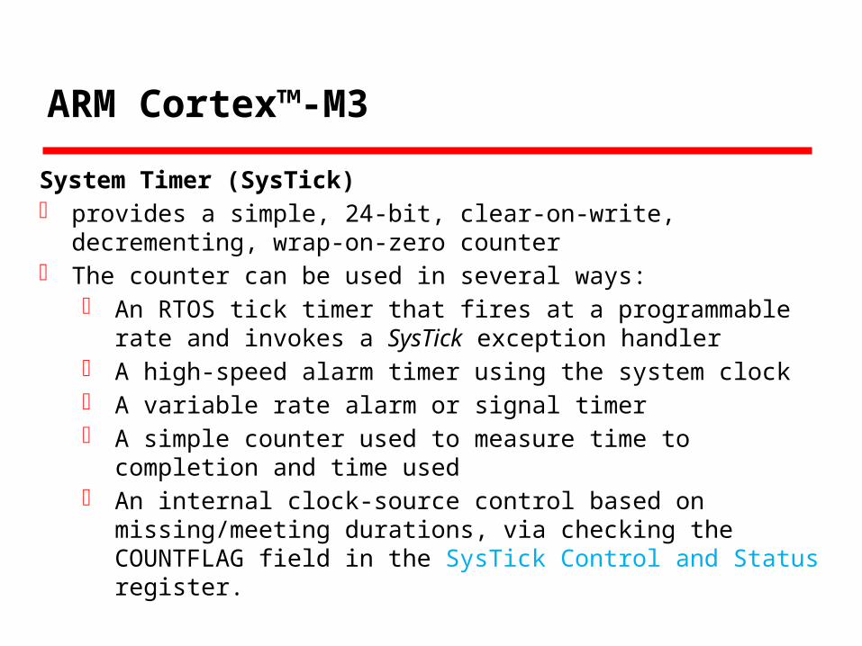
System Timer (SysTick) provides a simple, 24-bit, clear-on-write, decrementing, wrap-
on-zero counter The counter can be used in several ways:
An RTOS tick timer that fires at a programmable rate and invokes a SysTick exception handler
A high-speed alarm timer using the system clock A variable rate alarm or signal timer A simple counter used to measure time to completion and
time used An internal clock-source control based on missing/meeting
durations, via checking the COUNTFLAG field in the SysTick Control and Status register.
ARM Cortex™-M3
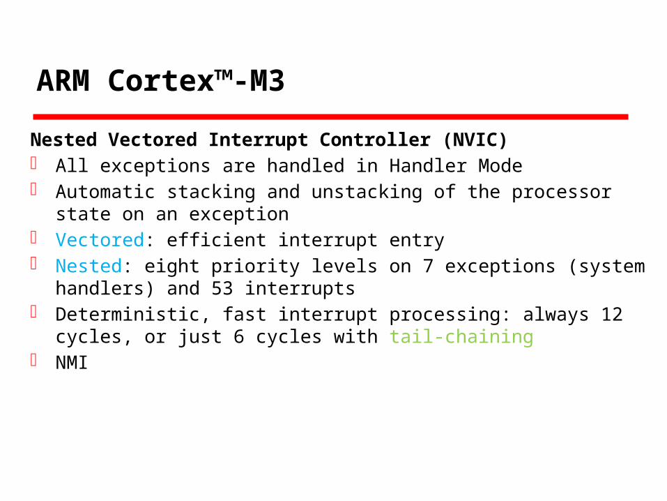
Nested Vectored Interrupt Controller (NVIC) All exceptions are handled in Handler Mode Automatic stacking and unstacking of the processor state on an
exception Vectored: efficient interrupt entry Nested: eight priority levels on 7 exceptions (system handlers)
and 53 interrupts Deterministic, fast interrupt processing: always 12 cycles, or
just 6 cycles with tail-chaining NMI
On-Chip Memory
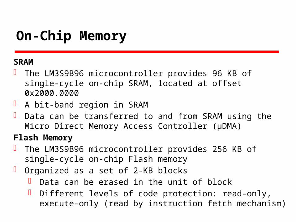
SRAM The LM3S9B96 microcontroller provides 96 KB of single-cycle
on-chip SRAM, located at offset 0x2000.0000 A bit-band region in SRAM Data can be transferred to and from SRAM using the Micro
Direct Memory Access Controller (μDMA)Flash Memory The LM3S9B96 microcontroller provides 256 KB of single-cycle
on-chip Flash memory Organized as a set of 2-KB blocks
Data can be erased in the unit of block Different levels of code protection: read-only, execute-only
(read by instruction fetch mechanism)
On-Chip Memory
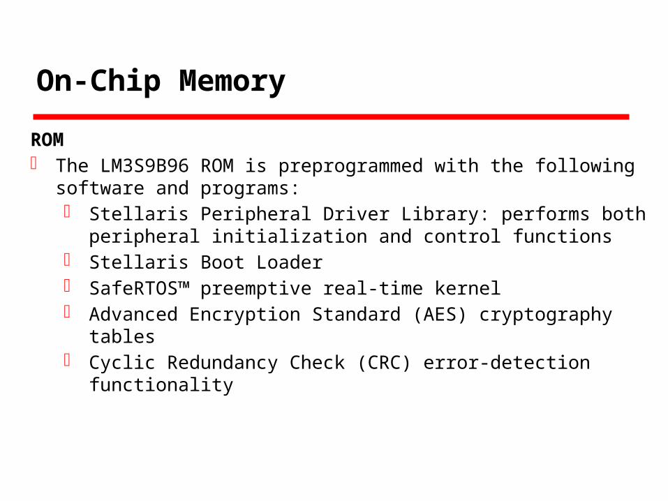
ROM The LM3S9B96 ROM is preprogrammed with the following
software and programs: Stellaris Peripheral Driver Library: performs both peripheral
initialization and control functions Stellaris Boot Loader SafeRTOS™ preemptive real-time kernel Advanced Encryption Standard (AES) cryptography tables Cyclic Redundancy Check (CRC) error-detection
functionality
External Peripheral Interface (EPI)
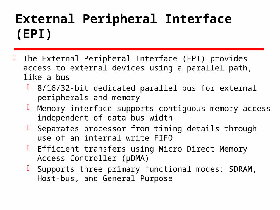
The External Peripheral Interface (EPI) provides access to external devices using a parallel path, like a bus 8/16/32-bit dedicated parallel bus for external peripherals
and memory Memory interface supports contiguous memory access
independent of data bus width Separates processor from timing details through use of an
internal write FIFO Efficient transfers using Micro Direct Memory Access
Controller (μDMA) Supports three primary functional modes: SDRAM, Host-
bus, and General Purpose
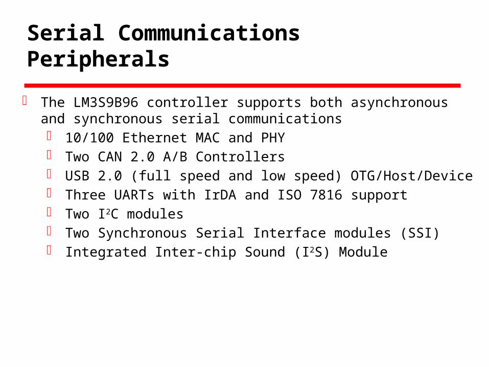
Serial Communications Peripherals
The LM3S9B96 controller supports both asynchronous and synchronous serial communications 10/100 Ethernet MAC and PHY Two CAN 2.0 A/B Controllers USB 2.0 (full speed and low speed) OTG/Host/Device Three UARTs with IrDA and ISO 7816 support Two I2C modules Two Synchronous Serial Interface modules (SSI) Integrated Inter-chip Sound (I2S) Module
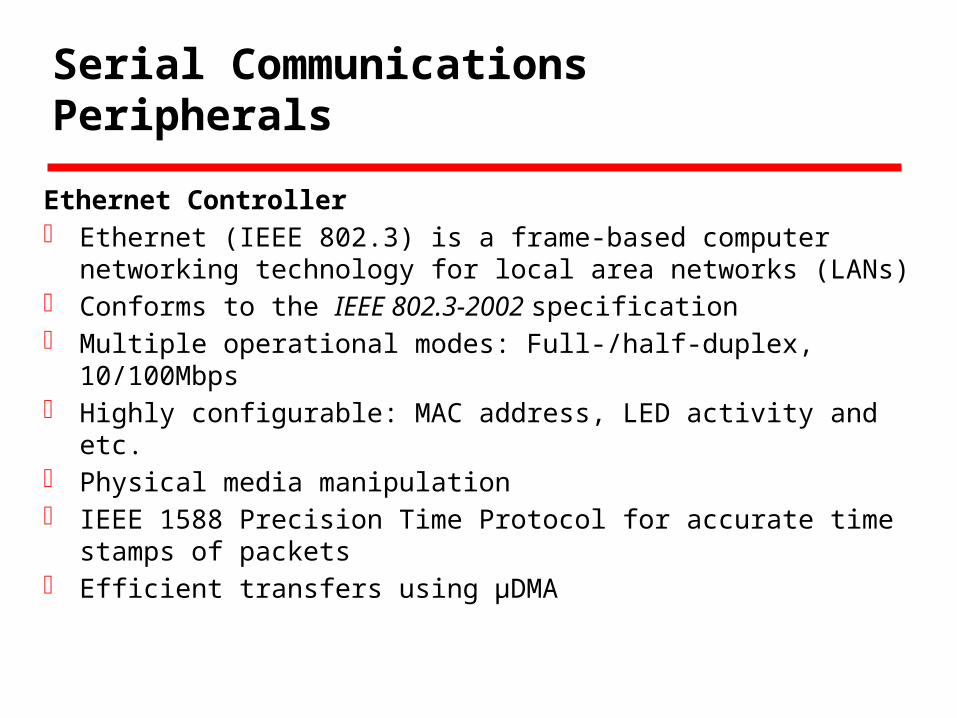
Serial Communications Peripherals
Ethernet Controller Ethernet (IEEE 802.3) is a frame-based computer networking
technology for local area networks (LANs) Conforms to the IEEE 802.3-2002 specification Multiple operational modes: Full-/half-duplex, 10/100Mbps Highly configurable: MAC address, LED activity and etc. Physical media manipulation IEEE 1588 Precision Time Protocol for accurate time stamps of
packets Efficient transfers using μDMA
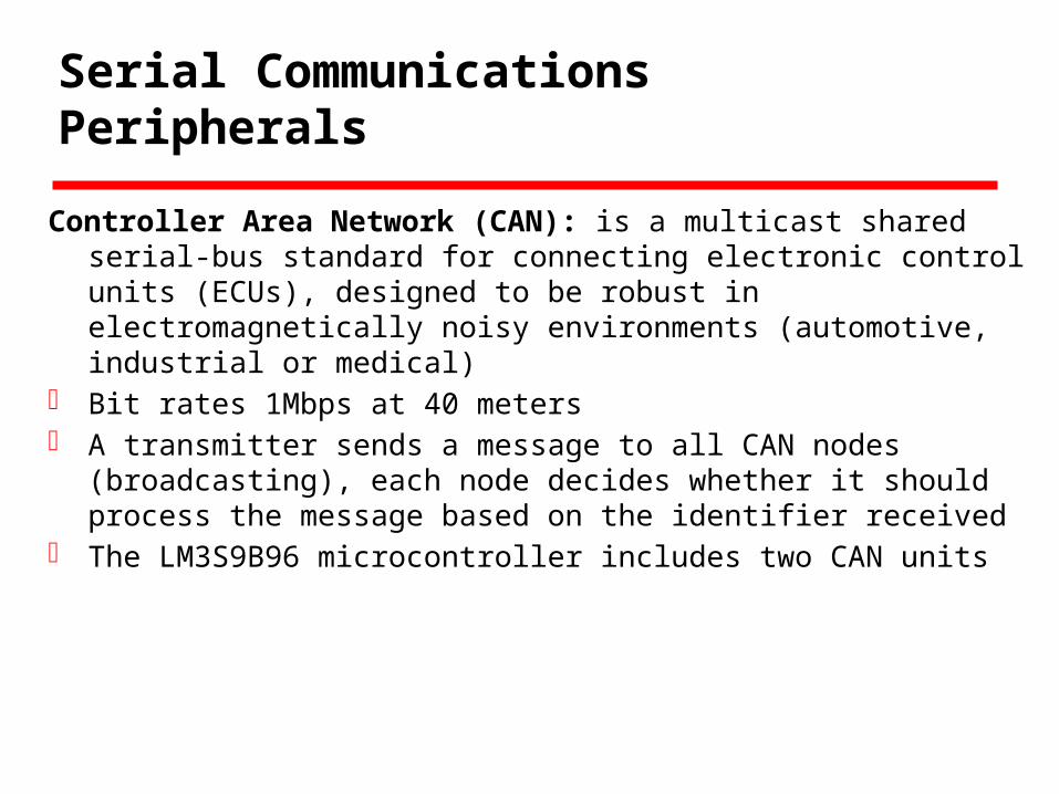
Serial Communications Peripherals
Controller Area Network (CAN): is a multicast shared serial-bus standard for connecting electronic control units (ECUs), designed to be robust in electromagnetically noisy environments (automotive, industrial or medical)
Bit rates 1Mbps at 40 meters A transmitter sends a message to all CAN nodes
(broadcasting), each node decides whether it should process the message based on the identifier received
The LM3S9B96 microcontroller includes two CAN units
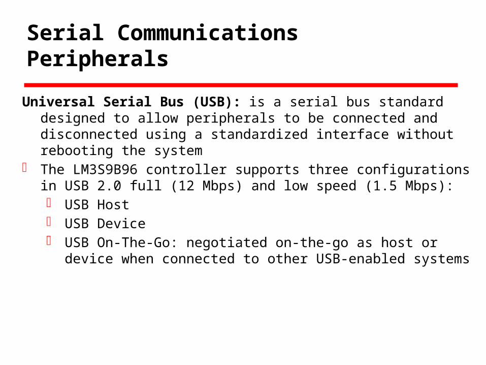
Serial Communications Peripherals
Universal Serial Bus (USB): is a serial bus standard designed to allow peripherals to be connected and disconnected using a standardized interface without rebooting the system
The LM3S9B96 controller supports three configurations in USB 2.0 full (12 Mbps) and low speed (1.5 Mbps): USB Host USB Device USB On-The-Go: negotiated on-the-go as host or device
when connected to other USB-enabled systems

Serial Communications Peripherals
Universal Asynchronous Receiver/Transmitter (UART): The LM3S9B96 controller includes three fully programmable
16C550-type UARTs. Key features:
Programmable baud-rate generator Standard asynchronous communication bits for start, stop,
and parity Fully programmable serial interface characteristics Full modem handshake support (on UART1) Efficient transfers using μDMA
Serial Communications Peripherals
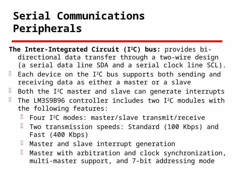
The Inter-Integrated Circuit (I2C) bus: provides bi-directional data transfer through a two-wire design (a serial data line SDA and a serial clock line SCL).
Each device on the I2C bus supports both sending and receiving data as either a master or a slave
Both the I2C master and slave can generate interrupts The LM3S9B96 controller includes two I2C modules with the
following features: Four I2C modes: master/slave transmit/receive Two transmission speeds: Standard (100 Kbps) and Fast
(400 Kbps) Master and slave interrupt generation Master with arbitration and clock synchronization, multi-
master support, and 7-bit addressing mode
Serial Communications Peripherals
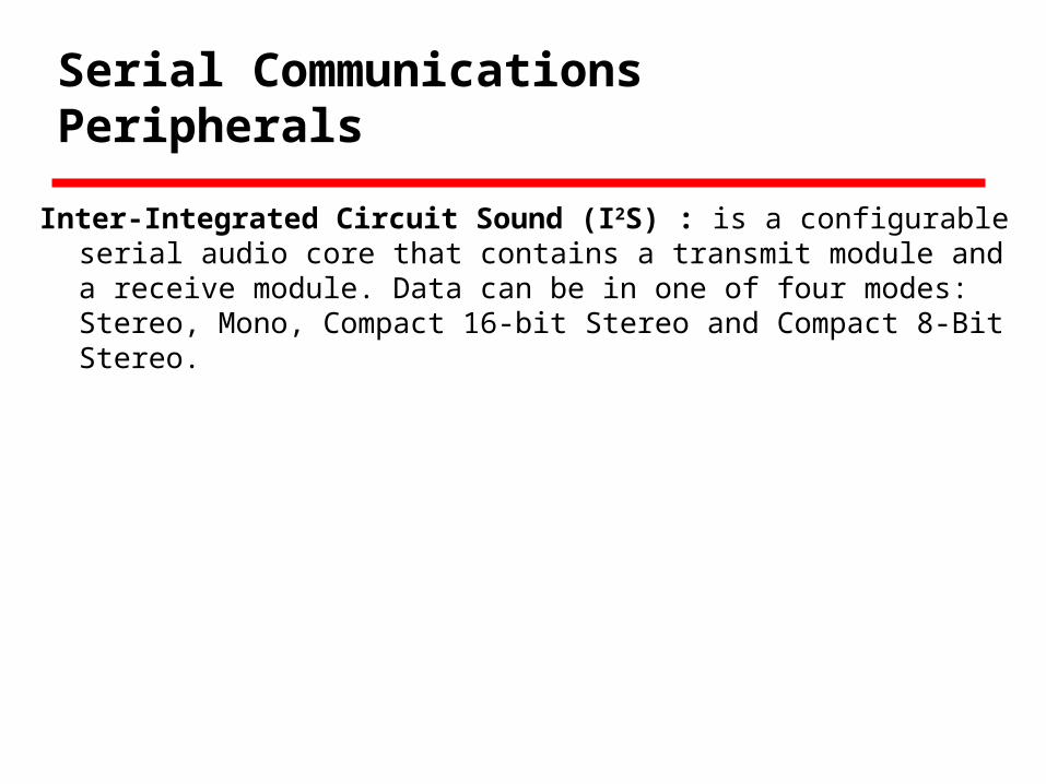
Inter-Integrated Circuit Sound (I2S) : is a configurable serial audio core that contains a transmit module and a receive module. Data can be in one of four modes: Stereo, Mono, Compact 16-bit Stereo and Compact 8-Bit Stereo.
System Integration
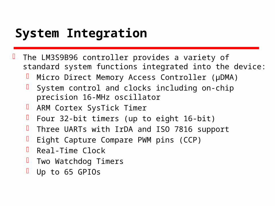
The LM3S9B96 controller provides a variety of standard system functions integrated into the device: Micro Direct Memory Access Controller (μDMA) System control and clocks including on-chip precision 16-
MHz oscillator ARM Cortex SysTick Timer Four 32-bit timers (up to eight 16-bit) Three UARTs with IrDA and ISO 7816 support Eight Capture Compare PWM pins (CCP) Real-Time Clock Two Watchdog Timers Up to 65 GPIOs
System Integration
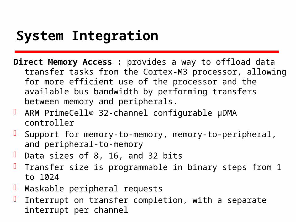
Direct Memory Access : provides a way to offload data transfer tasks from the Cortex-M3 processor, allowing for more efficient use of the processor and the available bus bandwidth by performing transfers between memory and peripherals.
ARM PrimeCell® 32-channel configurable μDMA controller Support for memory-to-memory, memory-to-peripheral, and
peripheral-to-memory Data sizes of 8, 16, and 32 bits Transfer size is programmable in binary steps from 1 to 1024 Maskable peripheral requests Interrupt on transfer completion, with a separate interrupt per
channel

System Integration
Direct Memory Access : provides a way to offload data transfer tasks from the Cortex-M3 processor, allowing for more efficient use of the processor and the available bus bandwidth by performing transfers between memory and peripherals.
ARM PrimeCell® 32-channel configurable μDMA controller Support for memory-to-memory, memory-to-peripheral, and
peripheral-to-memory Data sizes of 8, 16, and 32 bits Transfer size is programmable in binary steps from 1 to 1024 Maskable peripheral requests Interrupt on transfer completion, with a separate interrupt per
channel
System Integration
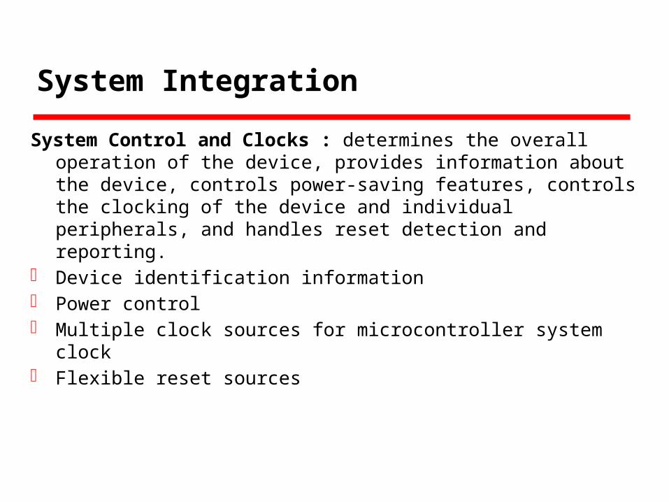
System Control and Clocks : determines the overall operation of the device, provides information about the device, controls power-saving features, controls the clocking of the device and individual peripherals, and handles reset detection and reporting.
Device identification information Power control Multiple clock sources for microcontroller system clock Flexible reset sources
System Integration
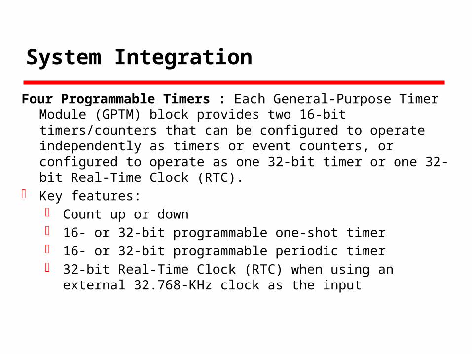
Four Programmable Timers : Each General-Purpose Timer Module (GPTM) block provides two 16-bit timers/counters that can be configured to operate independently as timers or event counters, or configured to operate as one 32-bit timer or one 32-bit Real-Time Clock (RTC).
Key features: Count up or down 16- or 32-bit programmable one-shot timer 16- or 32-bit programmable periodic timer 32-bit Real-Time Clock (RTC) when using an external
32.768-KHz clock as the input
System Integration
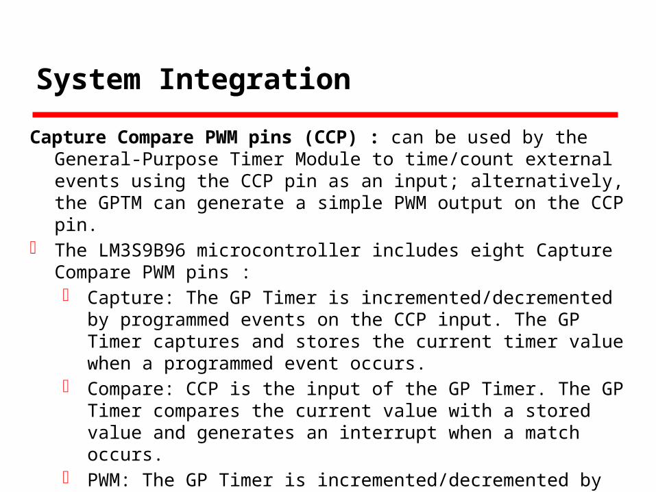
Capture Compare PWM pins (CCP) : can be used by the General-Purpose Timer Module to time/count external events using the CCP pin as an input; alternatively, the GPTM can generate a simple PWM output on the CCP pin.
The LM3S9B96 microcontroller includes eight Capture Compare PWM pins : Capture: The GP Timer is incremented/decremented by
programmed events on the CCP input. The GP Timer captures and stores the current timer value when a programmed event occurs.
Compare: CCP is the input of the GP Timer. The GP Timer compares the current value with a stored value and generates an interrupt when a match occurs.
PWM: The GP Timer is incremented/decremented by the system clock. A PWM signal is generated based on a match between the counter value and a value stored in a match register and is output on the CCP pin.
System Integration
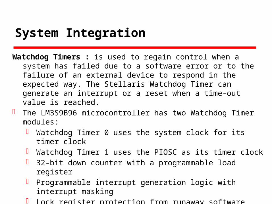
Watchdog Timers : is used to regain control when a system has failed due to a software error or to the failure of an external device to respond in the expected way. The Stellaris Watchdog Timer can generate an interrupt or a reset when a time-out value is reached.
The LM3S9B96 microcontroller has two Watchdog Timer modules: Watchdog Timer 0 uses the system clock for its timer clock Watchdog Timer 1 uses the PIOSC as its timer clock 32-bit down counter with a programmable load register Programmable interrupt generation logic with interrupt
masking Lock register protection from runaway software Reset generation logic with an enable/disable
System Integration
General-purpose input/output (GPIO) : offer flexibility for a variety of connections. The Stellaris GPIO module is comprised of nine physical GPIO blocks, each corresponding to an individual GPIO port, and supports 0-65 programmable input/output pins.
Key features: Up to 65 GPIOs, depending on configuration Highly flexible pin muxing Two means of port access: either Advanced High-
Performance Bus (AHB) or the legacy Advanced Peripheral Bus (APB) for backwards-compatibility
Programmable control for GPIO interrupts Bit masking in both read and write operations through
address lines Reset generation logic with an enable/disable Programmable control for GPIO pad configuration
Advanced Motion Control
The LM3S9B96 controller provides motion control functions integrated into the device, including:
Key features: Eight advanced PWM outputs for motion and energy
applications Two Quadrature Encoder Inputs (QEI)
Advanced Motion Control
Pulse width modulation (PWM): is a powerful technique for digitally encoding analog signal levels: High-resolution counters are used to generate a square wave, and the duty cycle of the square wave is modulated to encode an analog signal.
The LM3S9B96 PWM module consists of four PWM generator blocks: Four fault input to promote low-latency shutdown One 16-bit counter Two PWM comparators PWM signal generator Dead-band generator
One control block determines the polarity of the PWM signals and which signals are passed through to the pins.
Analog
The LM3S9B96 controller provides analog functions integrated into the device Two 10-bit Analog-to-Digital Converters (ADC) with sixteen
analog input channels and sample rate of one million samples/second
Three analog comparators 16 digital comparators On-chip voltage regulator
JTAG and ARM Serial Wire Debug
The Joint Test Action Group (JTAG) : is an IEEE standard that defines a Test Access Port and Boundary Scan Architecture for digital integrated circuits and provides a standardized serial interface for controlling the associated test logic.
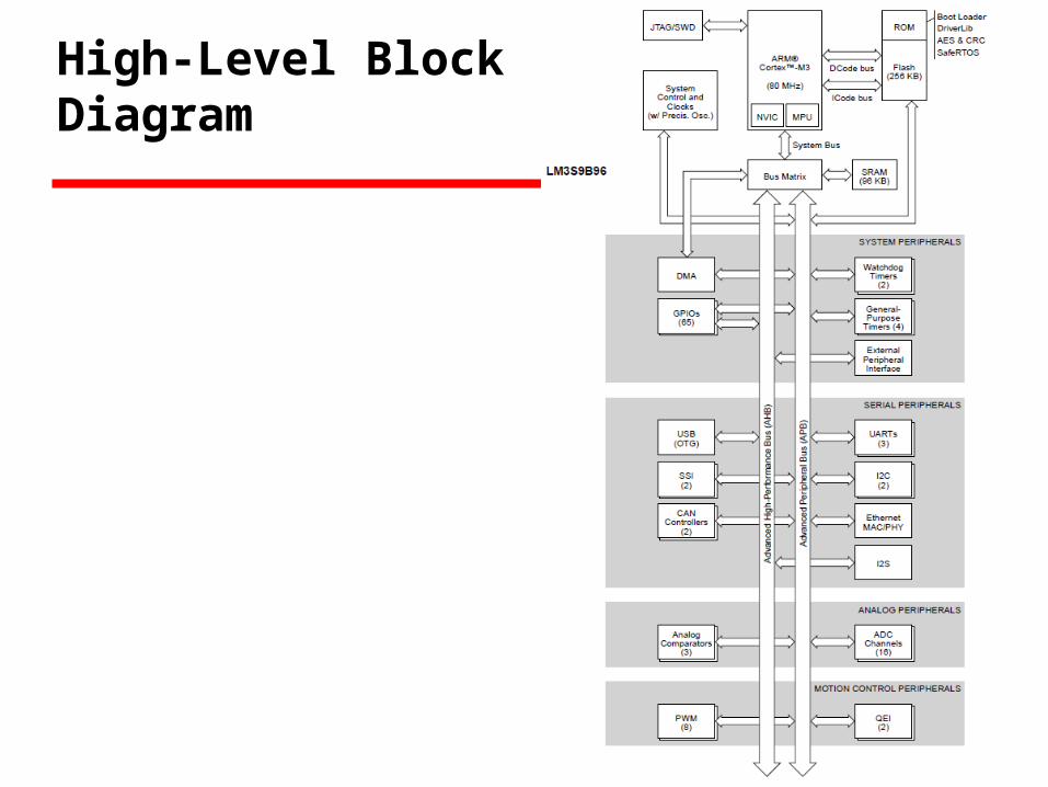
High-Level Block Diagram