Embed Size (px)
Citation preview
Graphics Processing Units (GPUs): Architecture and Programming
Mohamed Zahran (aka Z)
http://www.mzahran.com
CSCI-GA.3033-008
Lecture 2: Evolution of GPGPUs And Hardware Perspective
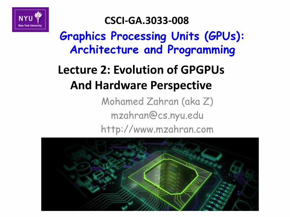
A Little Bit of Vocabulary
• Rendering: the process of generating an image from a model
• Vertex: the corner of a polygon (usually that polygon is a triangle)
• Pixel: smallest addressable screen element
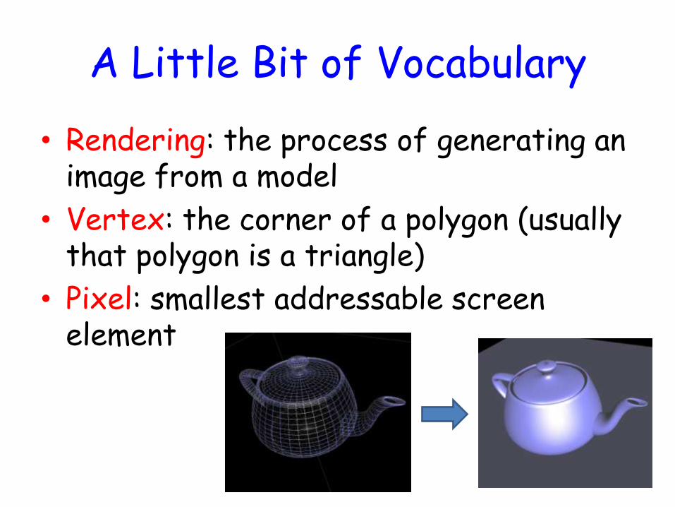
From Numbers to Screen
Before GPUs
• Vertices to pixels: – Transformations done on CPU
– Compute each pixel “by hand”, in series… slow!
Example: 1 million triangles * 100 pixels per triangle * 10 lights * 4 cycles per light computation = 4 billion cycles
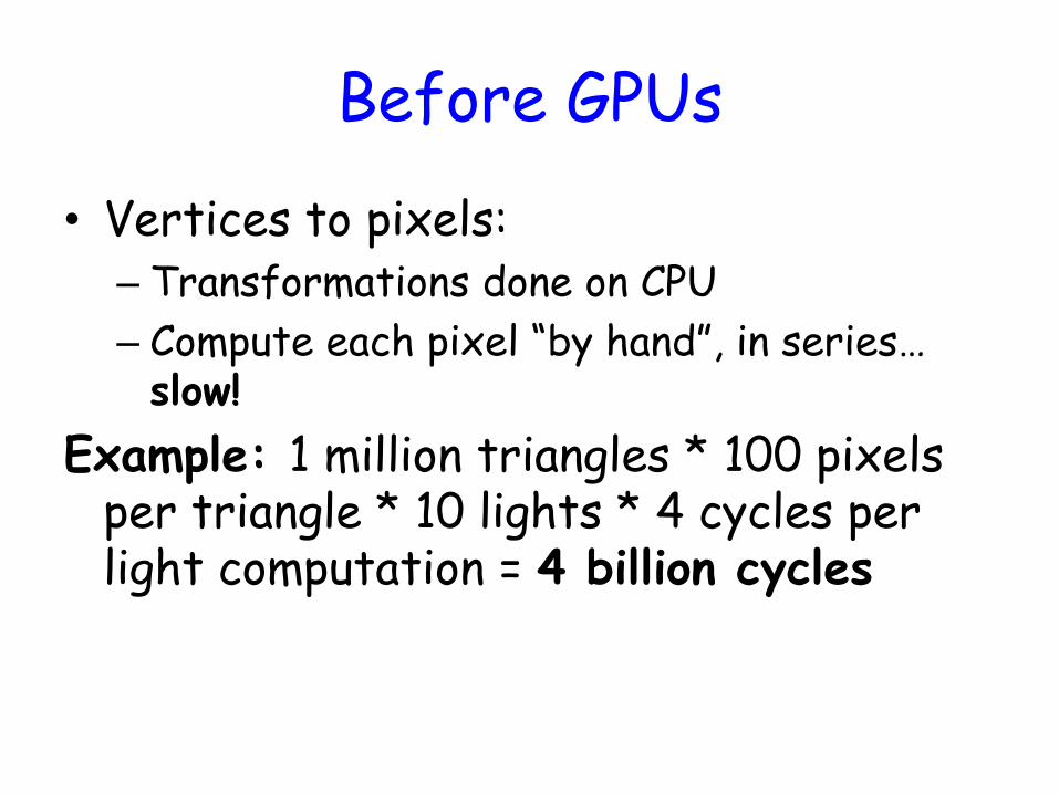
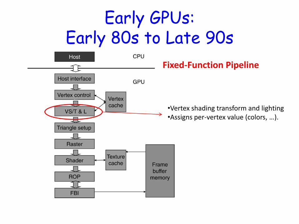
Early GPUs: Early 80s to Late 90s
Fixed-Function Pipeline
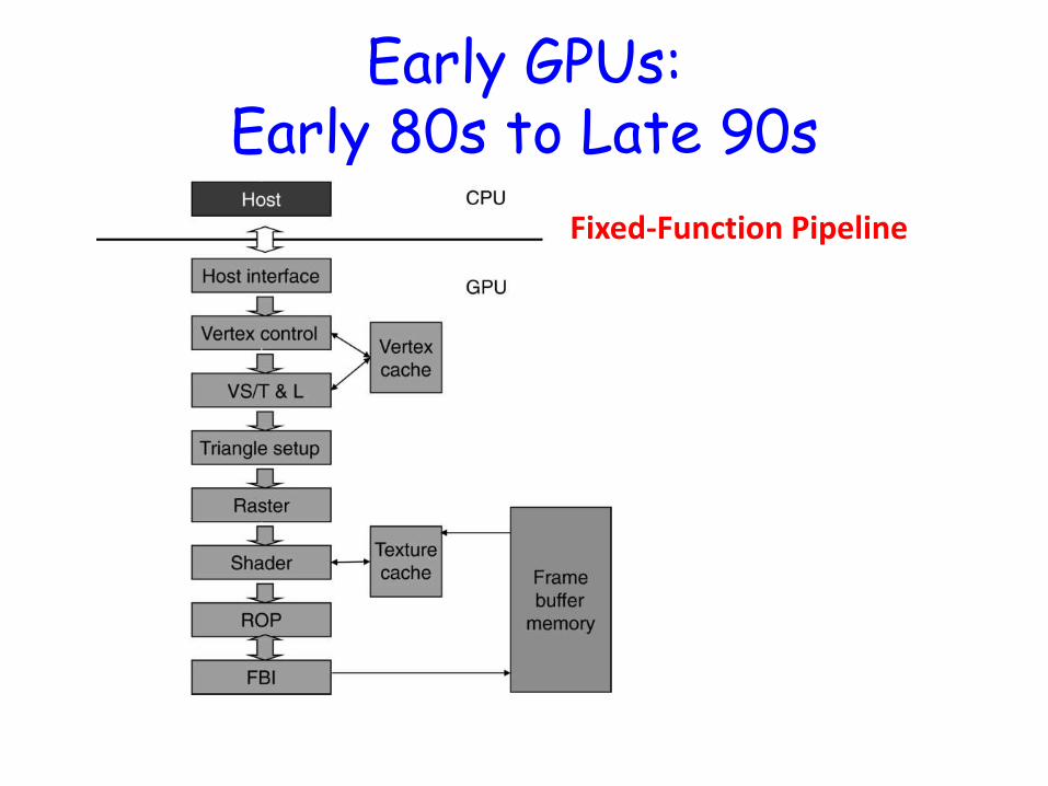
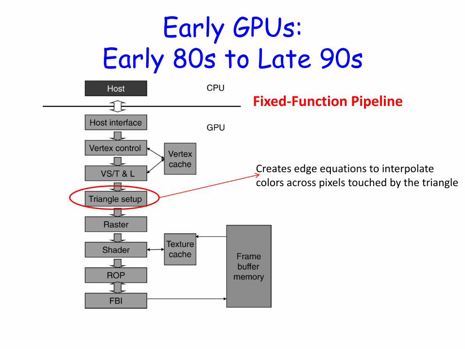
Early GPUs: Early 80s to Late 90s
Fixed-Function Pipeline
Receives graphics commands and data from CPU
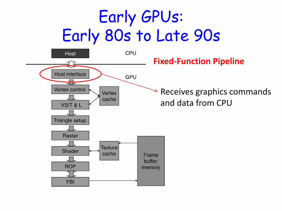
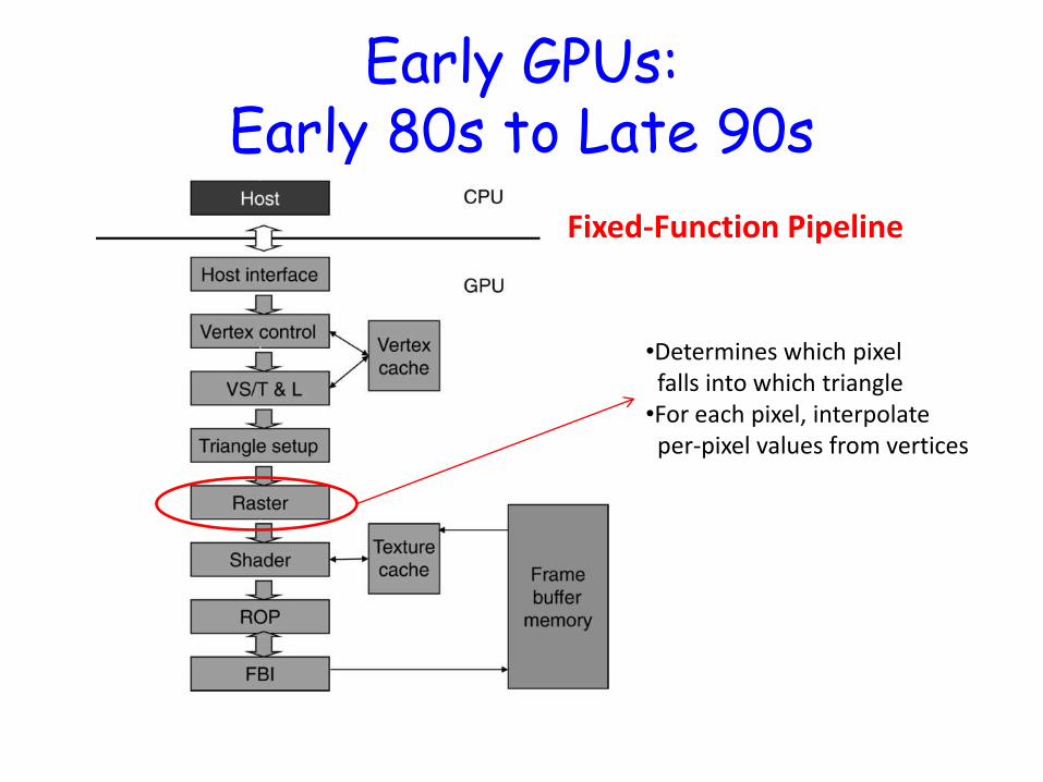
Early GPUs: Early 80s to Late 90s
Fixed-Function Pipeline
•Receives triangle data •Converts them into a form that hardware understands •Store the prepared data in vertex cache
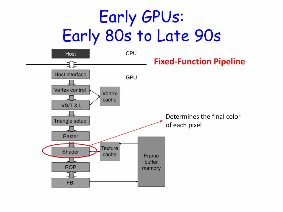
Early GPUs: Early 80s to Late 90s
Fixed-Function Pipeline
•Vertex shading transform and lighting •Assigns per-vertex value (colors, …).
Early GPUs: Early 80s to Late 90s
Fixed-Function Pipeline
Creates edge equations to interpolate colors across pixels touched by the triangle
Early GPUs: Early 80s to Late 90s
Fixed-Function Pipeline
•Determines which pixel falls into which triangle •For each pixel, interpolate per-pixel values from vertices
Early GPUs: Early 80s to Late 90s
Fixed-Function Pipeline
Determines the final color of each pixel
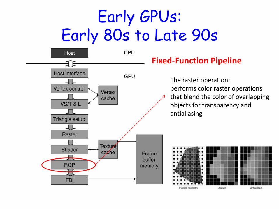
Early GPUs: Early 80s to Late 90s
Fixed-Function Pipeline
The raster operation: performs color raster operations that blend the color of overlapping objects for transparency and antialiasing
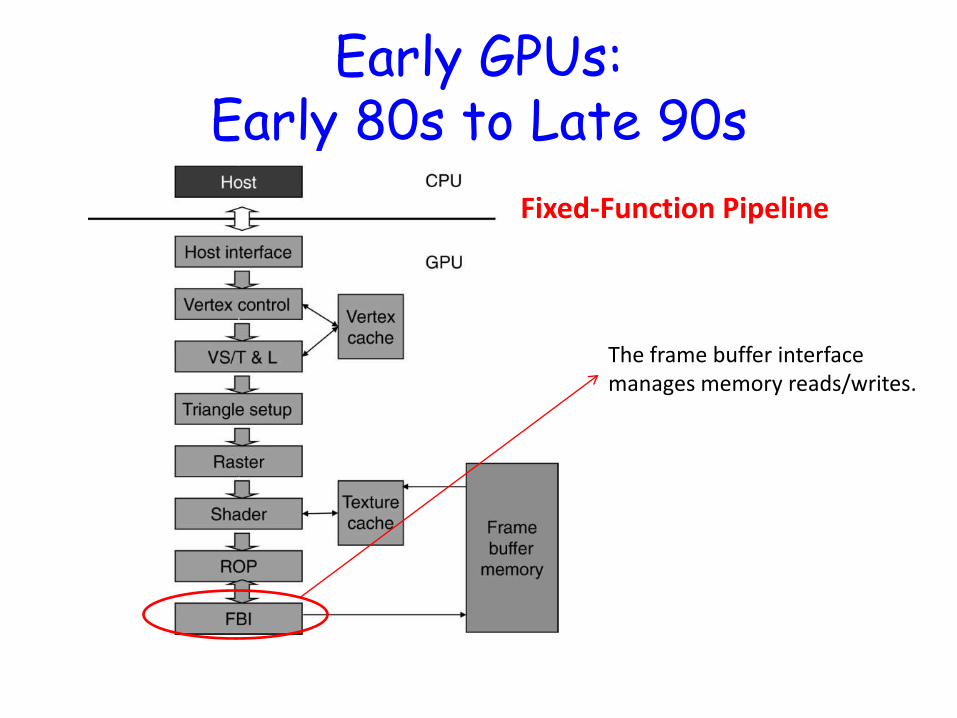
Early GPUs: Early 80s to Late 90s
Fixed-Function Pipeline
The frame buffer interface manages memory reads/writes.
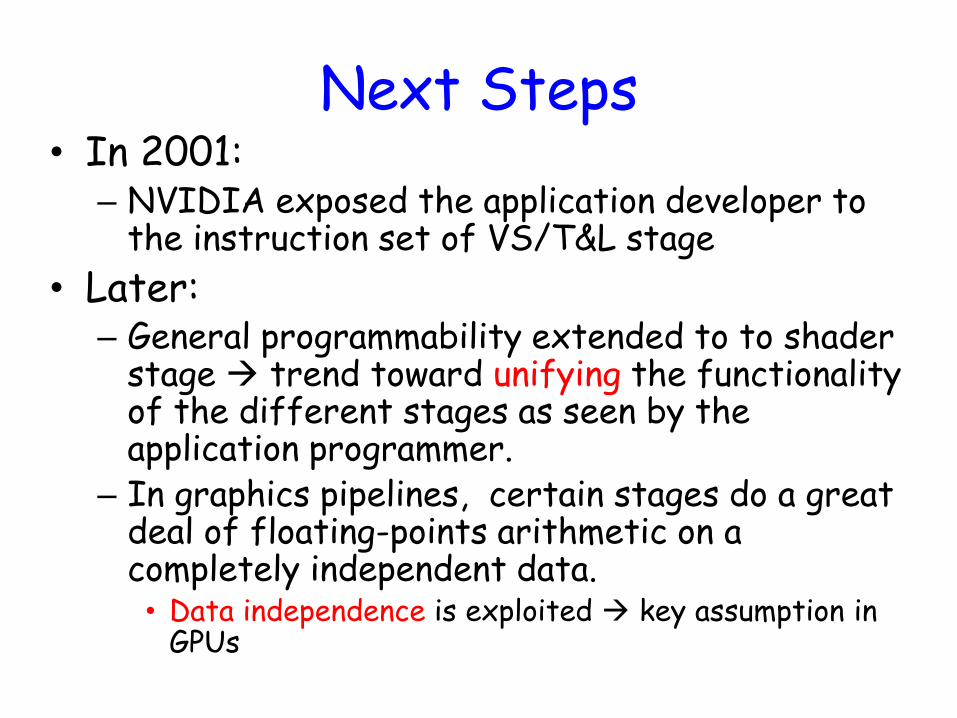
Next Steps • In 2001:
– NVIDIA exposed the application developer to the instruction set of VS/T&L stage
• Later: – General programmability extended to to shader
stage trend toward unifying the functionality of the different stages as seen by the application programmer.
– In graphics pipelines, certain stages do a great deal of floating-points arithmetic on a completely independent data. • Data independence is exploited key assumption in
GPUs
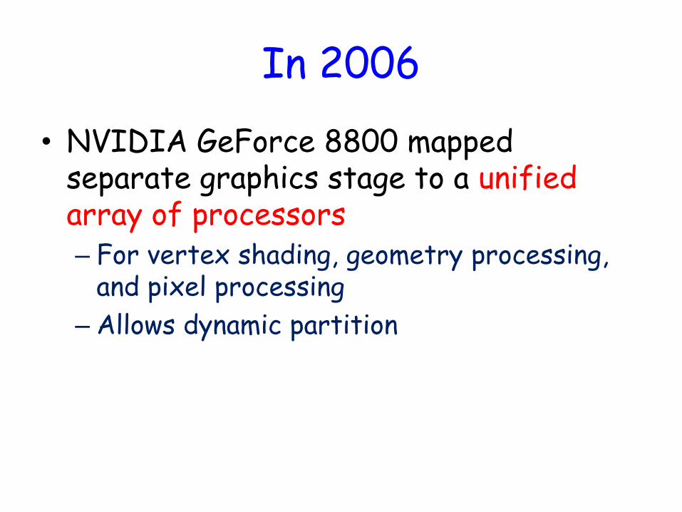
In 2006
• NVIDIA GeForce 8800 mapped separate graphics stage to a unified array of processors – For vertex shading, geometry processing,
and pixel processing
– Allows dynamic partition
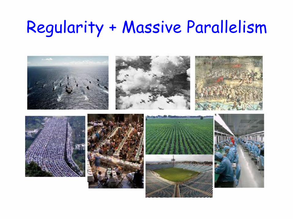
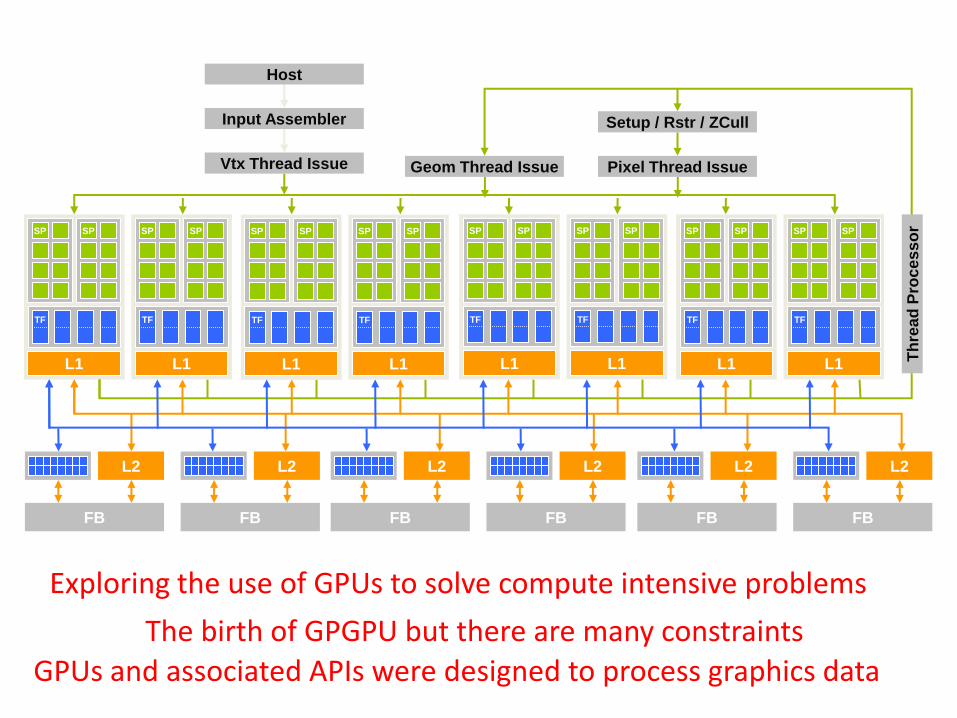
Regularity + Massive Parallelism
L2
FB
SP SP
L1
TF
Th
rea
d P
roc
es
so
r
Vtx Thread Issue
Setup / Rstr / ZCull
Geom Thread Issue Pixel Thread Issue
Input Assembler
Host
SP SP
L1
TF
SP SP
L1
TF
SP SP
L1
TF
SP SP
L1
TF
SP SP
L1
TF
SP SP
L1
TF
SP SP
L1
TF
L2
FB
L2
FB
L2
FB
L2
FB
L2
FB
Exploring the use of GPUs to solve compute intensive problems
GPUs and associated APIs were designed to process graphics data The birth of GPGPU but there are many constraints
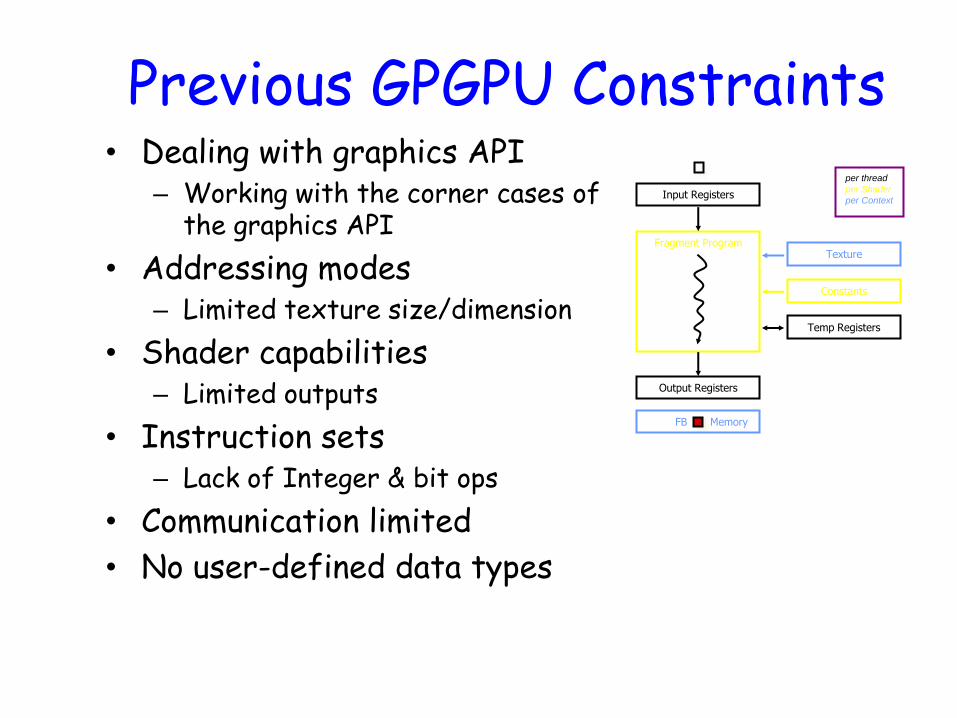
Previous GPGPU Constraints • Dealing with graphics API
– Working with the corner cases of the graphics API
• Addressing modes – Limited texture size/dimension
• Shader capabilities – Limited outputs
• Instruction sets – Lack of Integer & bit ops
• Communication limited
• No user-defined data types
Input Registers
Fragment Program
Output Registers
Constants
Texture
Temp Registers
per thread
per Shader
per Context
FB Memory
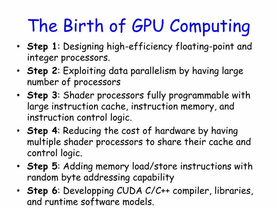
The Birth of GPU Computing • Step 1: Designing high-efficiency floating-point and
integer processors.
• Step 2: Exploiting data parallelism by having large number of processors
• Step 3: Shader processors fully programmable with large instruction cache, instruction memory, and instruction control logic.
• Step 4: Reducing the cost of hardware by having multiple shader processors to share their cache and control logic.
• Step 5: Adding memory load/store instructions with random byte addressing capability
• Step 6: Developping CUDA C/C++ compiler, libraries, and runtime software models.
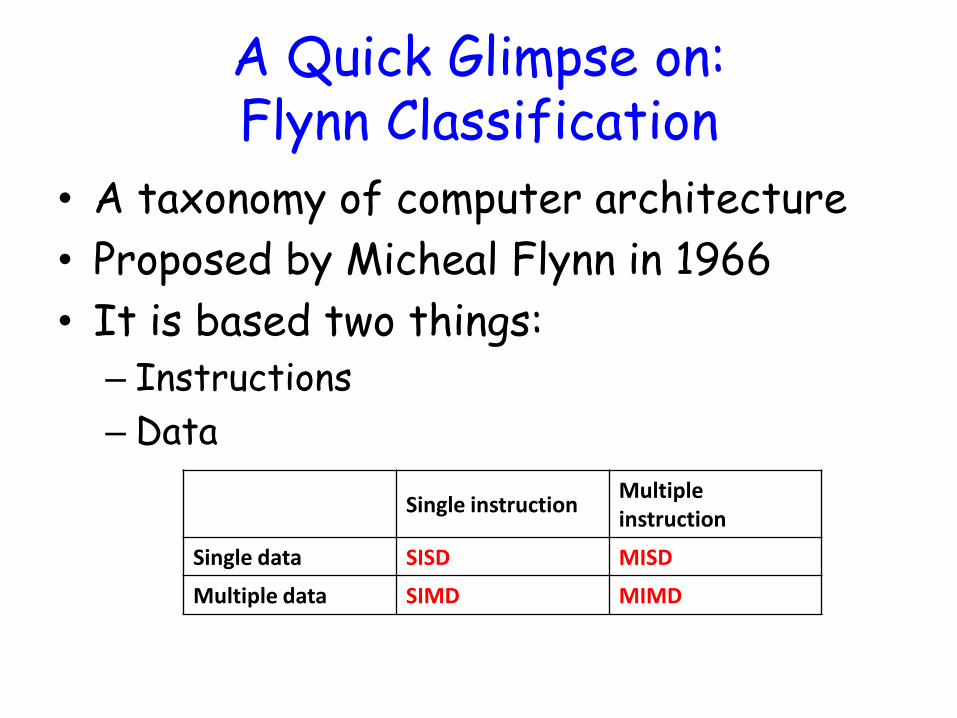
A Quick Glimpse on: Flynn Classification
• A taxonomy of computer architecture
• Proposed by Micheal Flynn in 1966
• It is based two things: – Instructions
– Data
Single instruction Multiple instruction
Single data SISD MISD
Multiple data SIMD MIMD
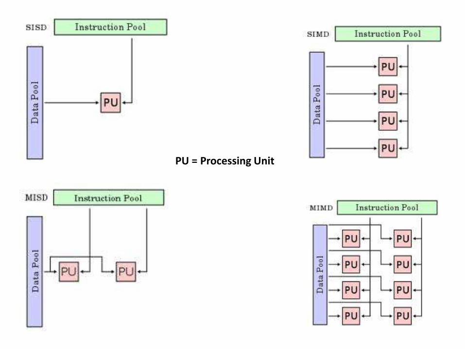
PU = Processing Unit
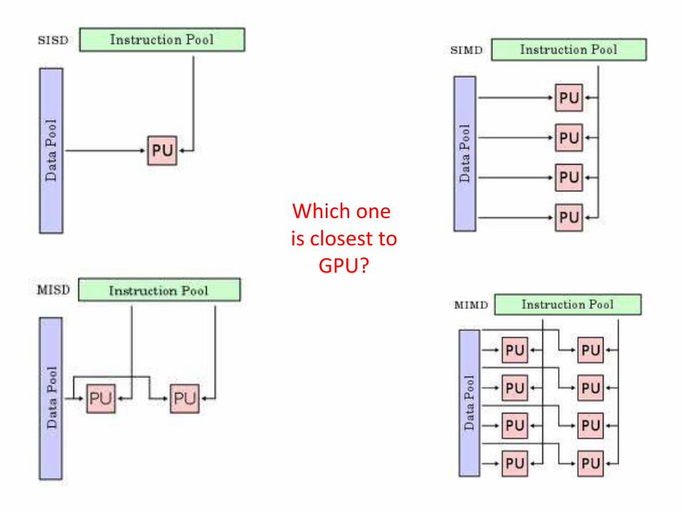
Which one is closest to
GPU?
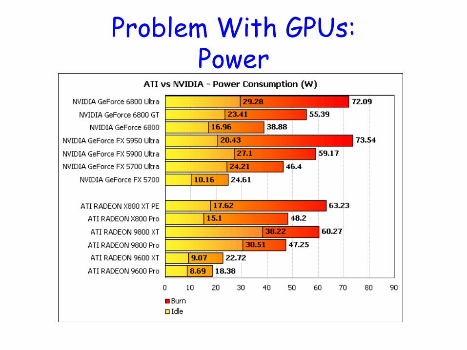
Problem With GPUs: Power
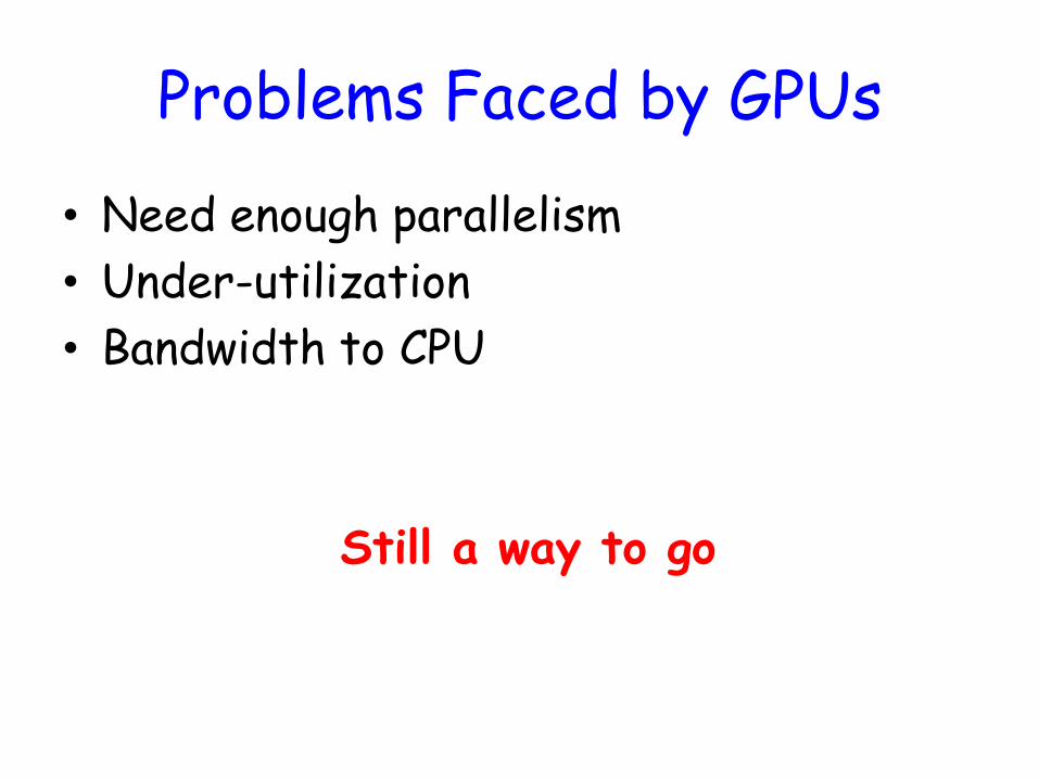
Problems Faced by GPUs
• Need enough parallelism
• Under-utilization
• Bandwidth to CPU
Still a way to go

Let’s Take A Closer Look: The Hardware
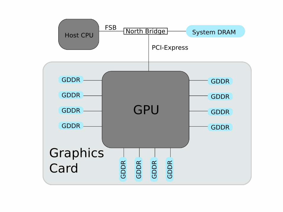
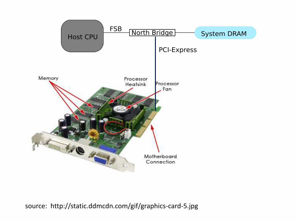
source: http://static.ddmcdn.com/gif/graphics-card-5.jpg
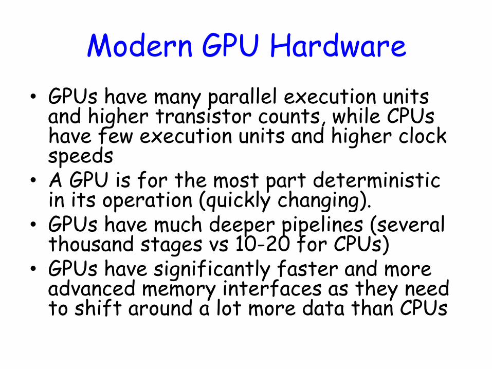
Modern GPU Hardware
• GPUs have many parallel execution units and higher transistor counts, while CPUs have few execution units and higher clock speeds
• A GPU is for the most part deterministic in its operation (quickly changing).
• GPUs have much deeper pipelines (several thousand stages vs 10-20 for CPUs)
• GPUs have significantly faster and more advanced memory interfaces as they need to shift around a lot more data than CPUs
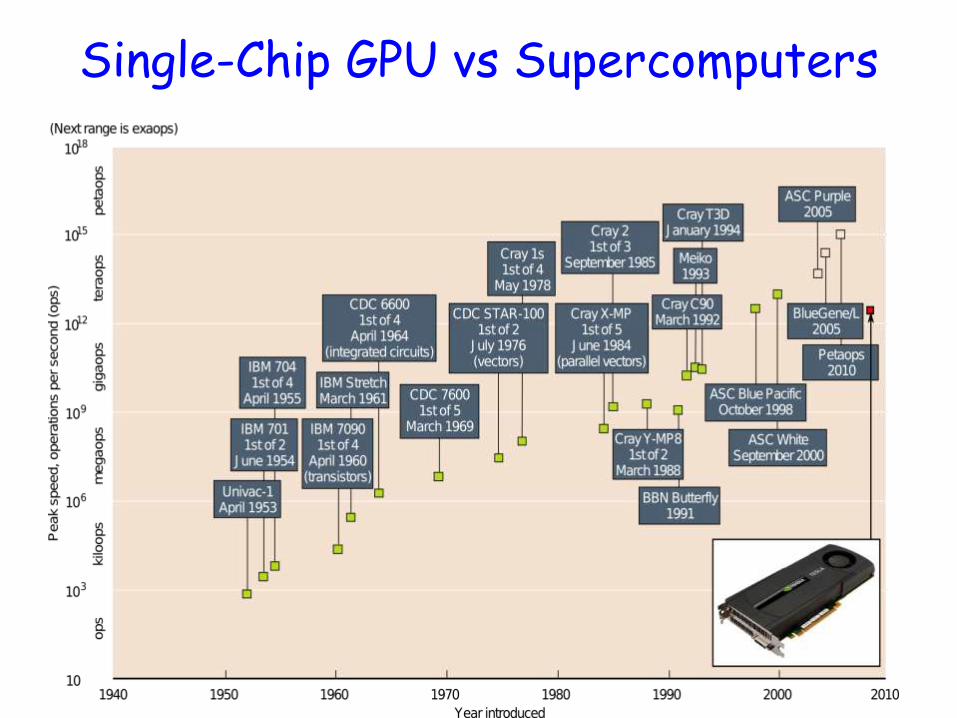
Single-Chip GPU vs Supercomputers
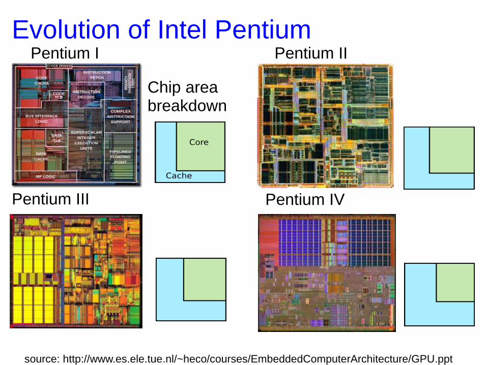
Evolution of Intel Pentium Pentium I Pentium II
Pentium III Pentium IV
Chip area breakdown
source: http://www.es.ele.tue.nl/~heco/courses/EmbeddedComputerArchitecture/GPU.ppt
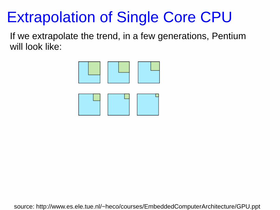
Extrapolation of Single Core CPU If we extrapolate the trend, in a few generations, Pentium will look like:
source: http://www.es.ele.tue.nl/~heco/courses/EmbeddedComputerArchitecture/GPU.ppt
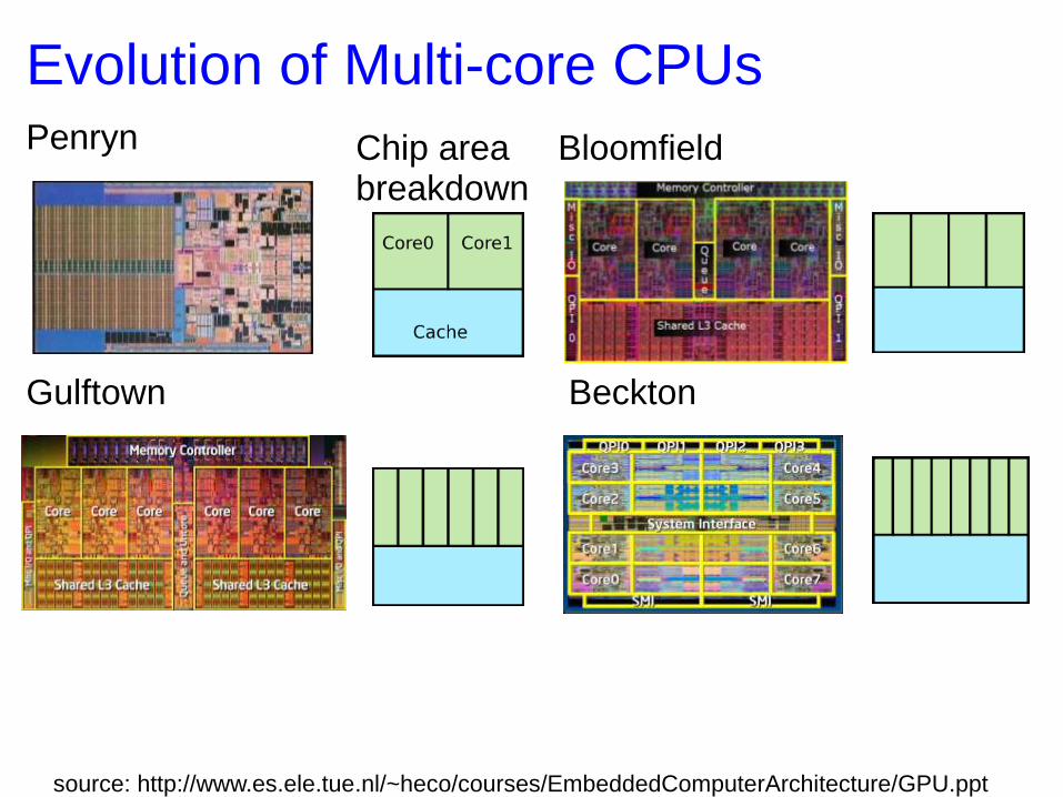
Evolution of Multi-core CPUs Penryn Bloomfield
Gulftown Beckton
Chip area breakdown
source: http://www.es.ele.tue.nl/~heco/courses/EmbeddedComputerArchitecture/GPU.ppt
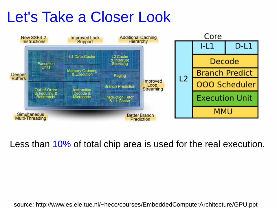
Let's Take a Closer Look
Less than 10% of total chip area is used for the real execution.
source: http://www.es.ele.tue.nl/~heco/courses/EmbeddedComputerArchitecture/GPU.ppt
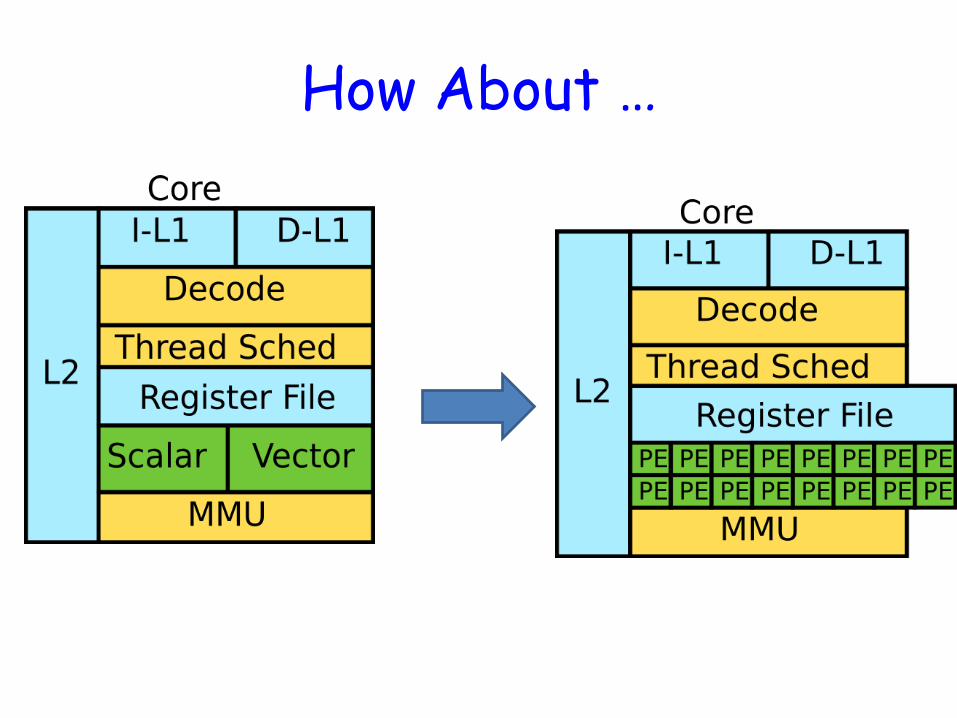
How About …
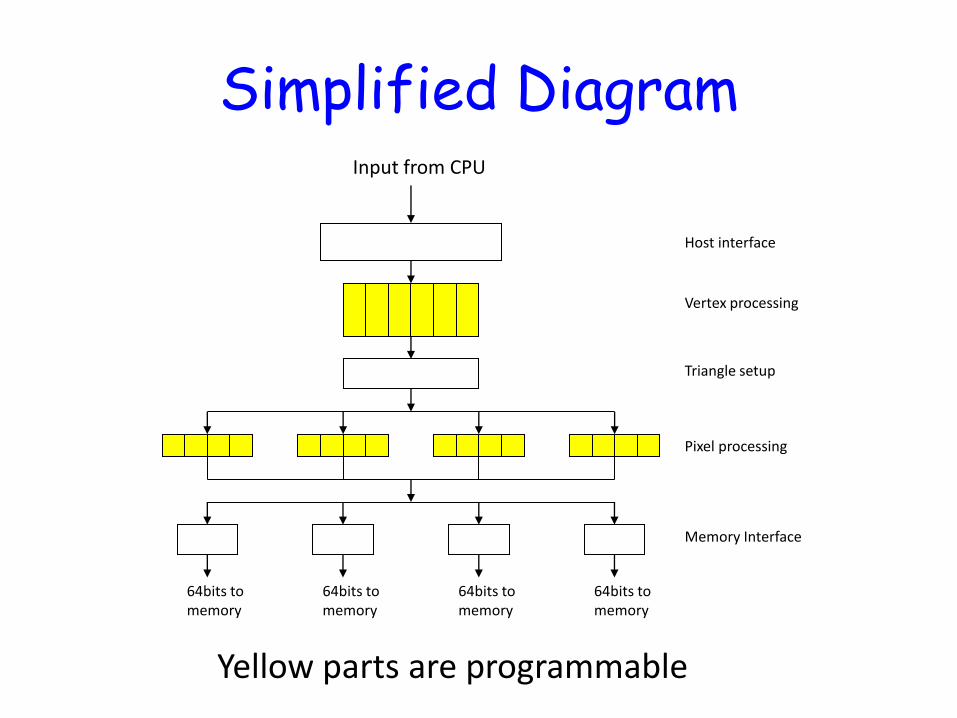
Simplified Diagram
64bits to memory
64bits to memory
64bits to memory
64bits to memory
Input from CPU
Host interface
Vertex processing
Triangle setup
Pixel processing
Memory Interface
Yellow parts are programmable
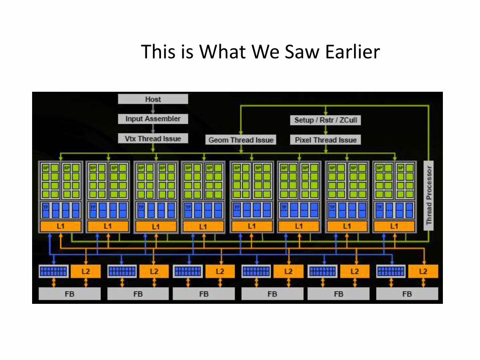
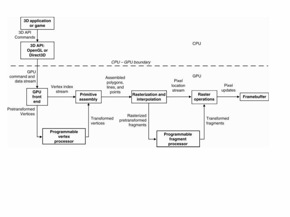
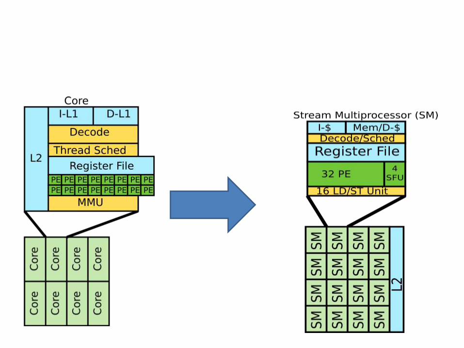
This is What We Saw Earlier
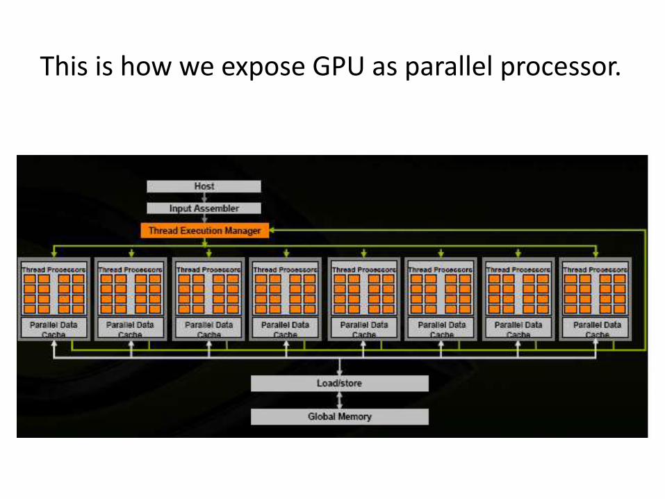
This is how we expose GPU as parallel processor.
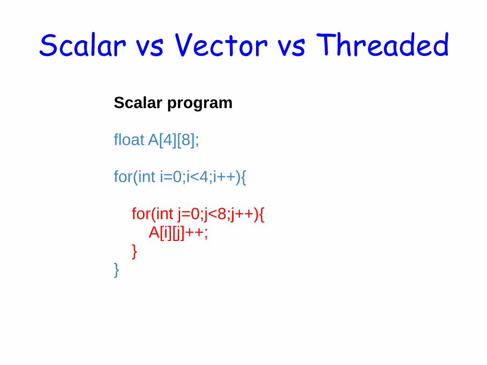
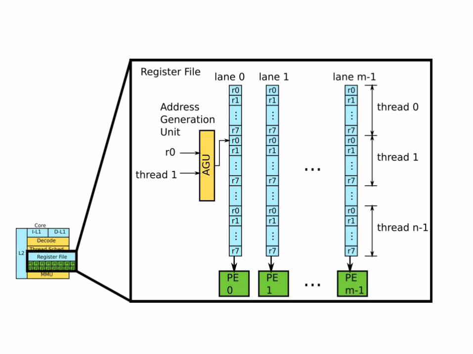
Scalar vs Vector vs Threaded
Scalar program float A[4][8]; for(int i=0;i<4;i++){ for(int j=0;j<8;j++){ A[i][j]++; } }
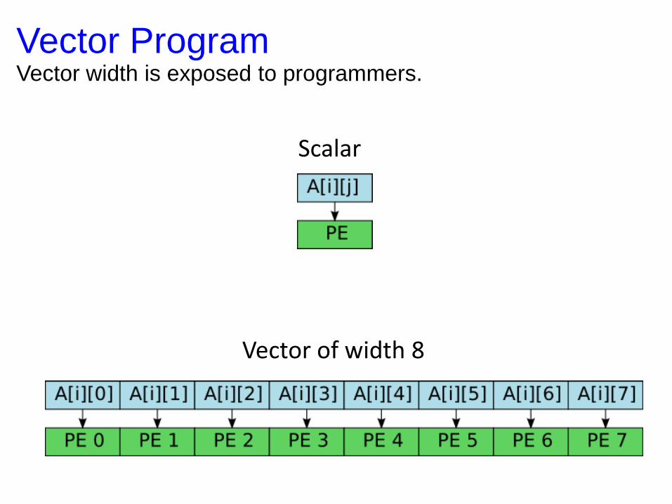
Vector Program Vector width is exposed to programmers.
Scalar
Vector of width 8
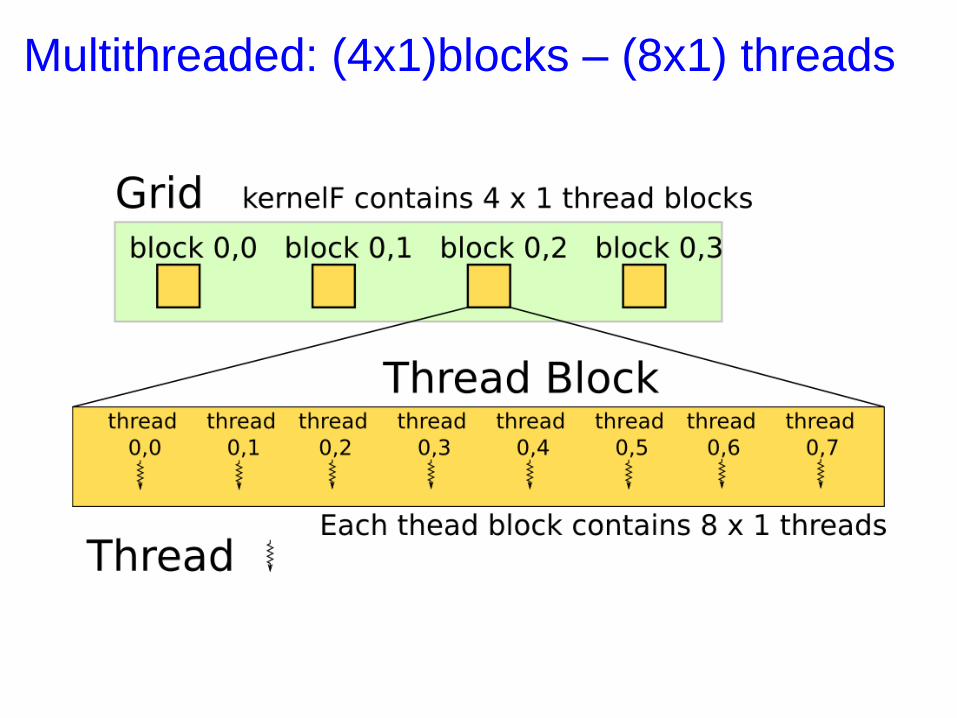
Multithreaded: (4x1)blocks – (8x1) threads
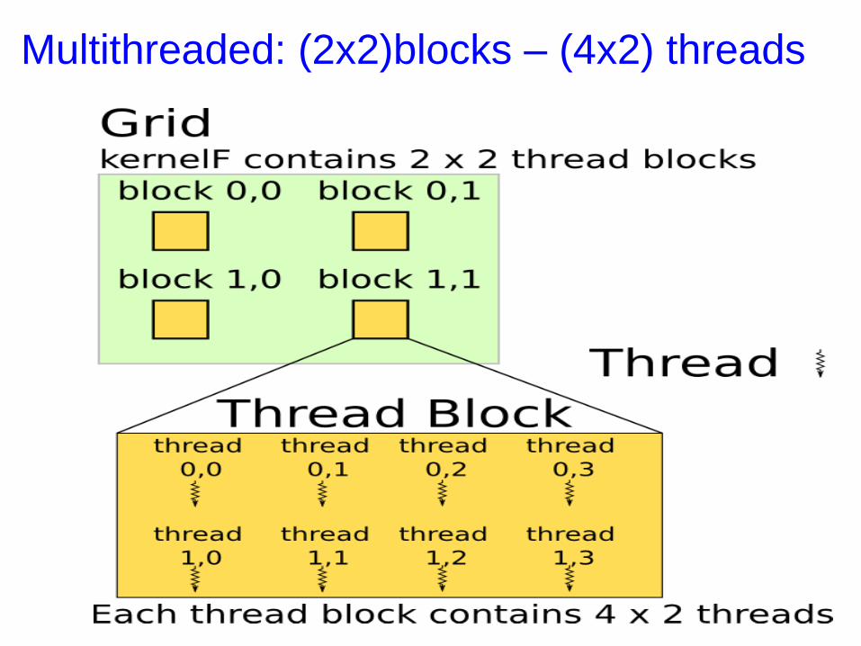
Multithreaded: (2x2)blocks – (4x2) threads
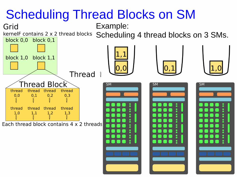
Scheduling Thread Blocks on SM Example: Scheduling 4 thread blocks on 3 SMs.
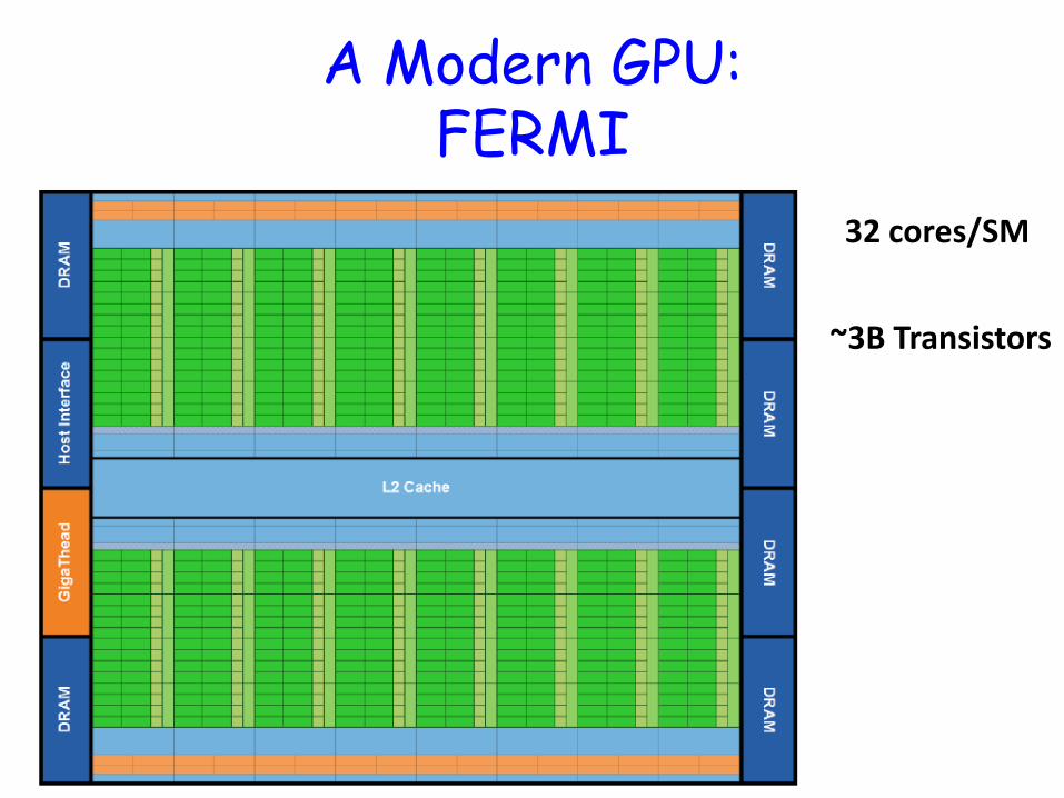
A Modern GPU: FERMI
32 cores/SM
~3B Transistors
Main Goals of Fermi
• Increasing floating-point throughput
• Allowing software developers to focus on algorithm design rather than the details of how to map the algorithm to the hardware
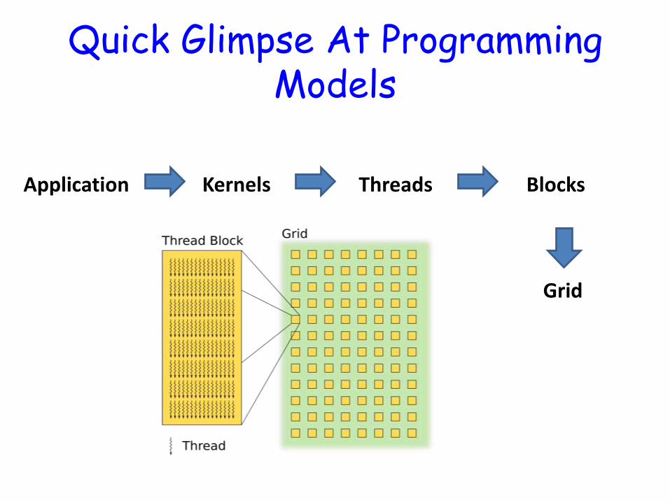
Quick Glimpse At Programming Models
Application Kernels
Grid
Blocks Threads
Quick Glimpse At Programming Models
• Application can include multiple kernels • Threads of the same block run on the same SM
– So threads in SM can operate and share memory – Block in an SM is divided into warps of 32 threads
each – A warp is the fundamental unit of dispatch in an
SM
• Blocks in a grid can coordinate using global shared memory
• Each grid executes a kernel
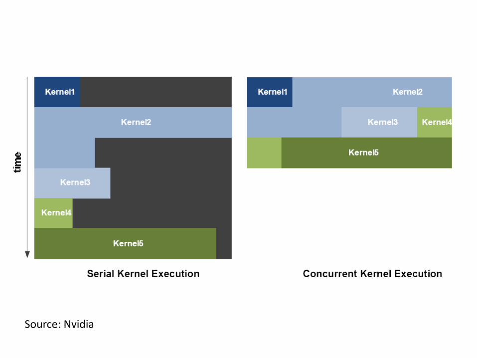
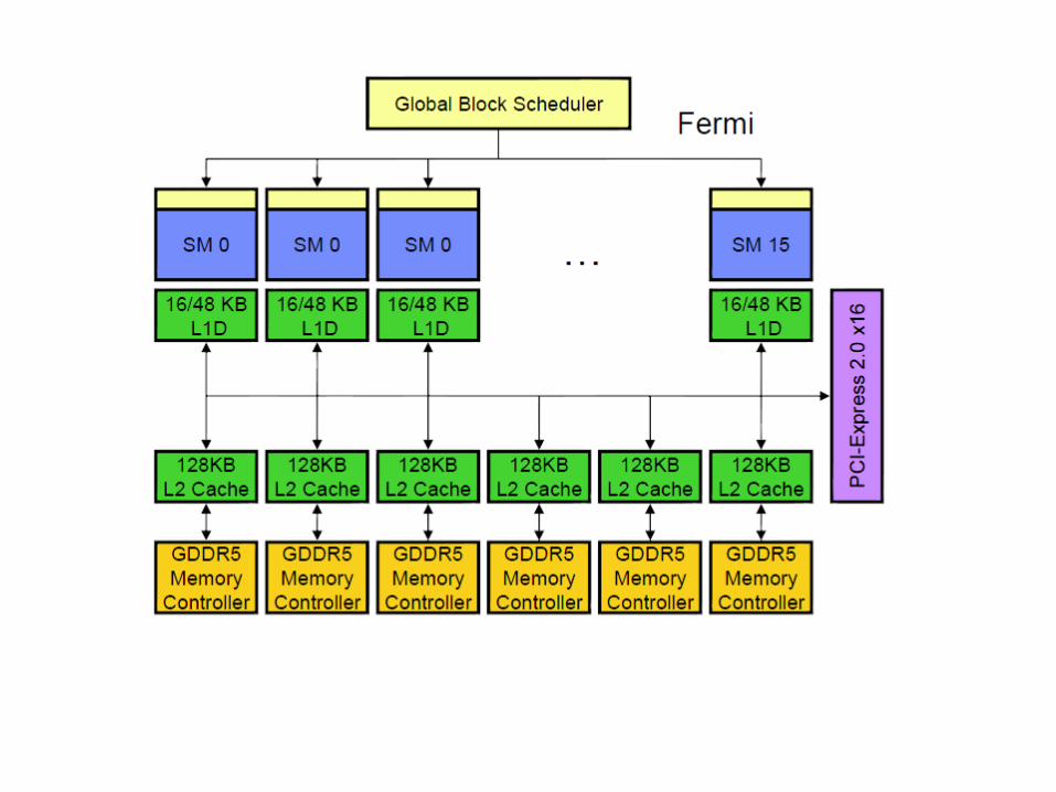
Scheduling In Fermi
• At any point of time the entire Fermi device is dedicated to a single application – Switch from an application to another takes
~25 microseconds
• Fermi can simultaneously execute multiple kernels of the same application
• Two warps from different blocks (or even different kernels) can be issued and executed simultaneously
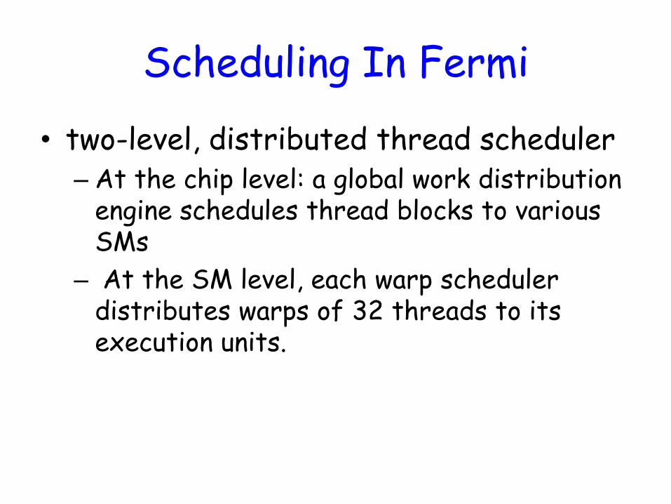
Scheduling In Fermi
• two-level, distributed thread scheduler – At the chip level: a global work distribution
engine schedules thread blocks to various SMs
– At the SM level, each warp scheduler distributes warps of 32 threads to its execution units.
Source: Nvidia
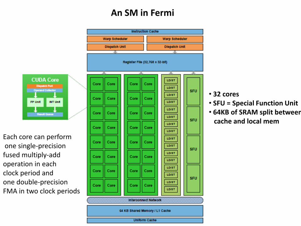
An SM in Fermi
• 32 cores • SFU = Special Function Unit • 64KB of SRAM split between cache and local mem
Each core can perform one single-precision fused multiply-add operation in each clock period and one double-precision FMA in two clock periods
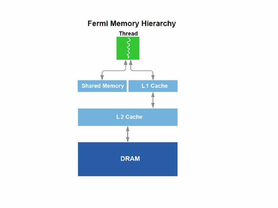
The Memory Hierarchy
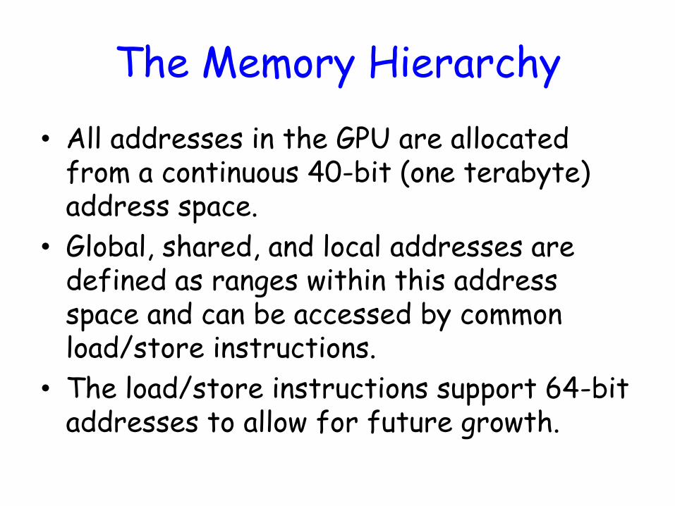
• All addresses in the GPU are allocated from a continuous 40-bit (one terabyte) address space.
• Global, shared, and local addresses are defined as ranges within this address space and can be accessed by common load/store instructions.
• The load/store instructions support 64-bit addresses to allow for future growth.
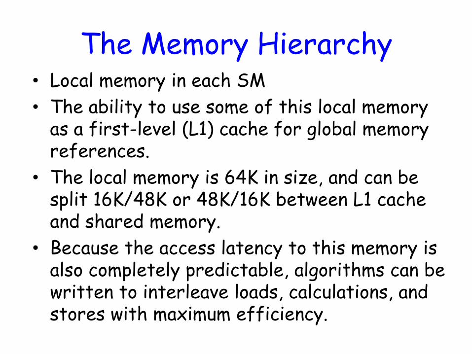
The Memory Hierarchy • Local memory in each SM
• The ability to use some of this local memory as a first-level (L1) cache for global memory references.
• The local memory is 64K in size, and can be split 16K/48K or 48K/16K between L1 cache and shared memory.
• Because the access latency to this memory is also completely predictable, algorithms can be written to interleave loads, calculations, and stores with maximum efficiency.
The Memory Hierarchy
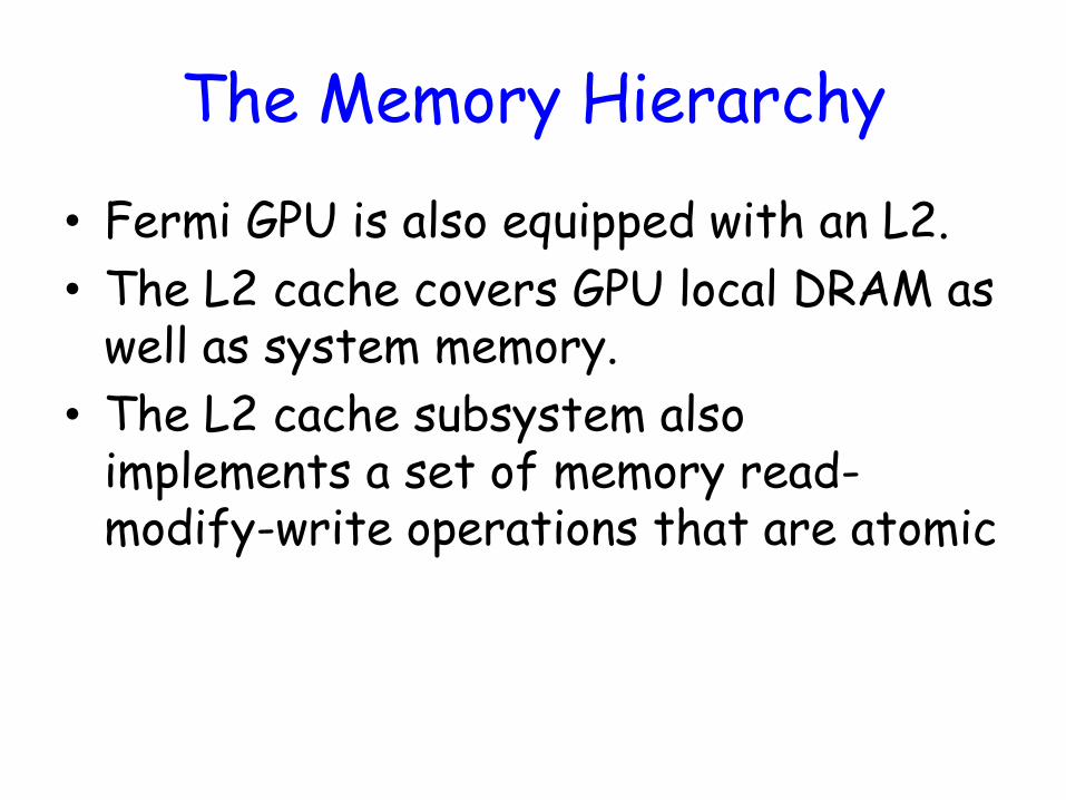
• Fermi GPU is also equipped with an L2.
• The L2 cache covers GPU local DRAM as well as system memory.
• The L2 cache subsystem also implements a set of memory read-modify-write operations that are atomic
Conclusions
• The design of state-of-the art GPUs includes: – Data parallelism
– Programmability
– Much less restrictive instruction set
• By looking at the hardware features, can you see how you can write more efficient programs for GPUs?