Embed Size (px)
Citation preview
Lecture 2: Field Programmable Gate Arrays September 13, 2004
ECE 697F
Reconfigurable Computing
Lecture 2
Field Programmable Gate Arrays
Lecture 2: Field Programmable Gate Arrays September 13, 2004
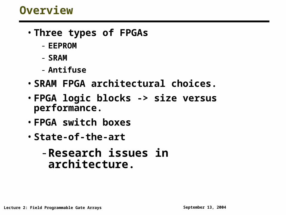
Overview
• Three types of FPGAs- EEPROM
- SRAM
- Antifuse
• SRAM FPGA architectural choices.
• FPGA logic blocks -> size versus performance.
• FPGA switch boxes
• State-of-the-art
- Research issues in architecture.
Lecture 2: Field Programmable Gate Arrays September 13, 2004
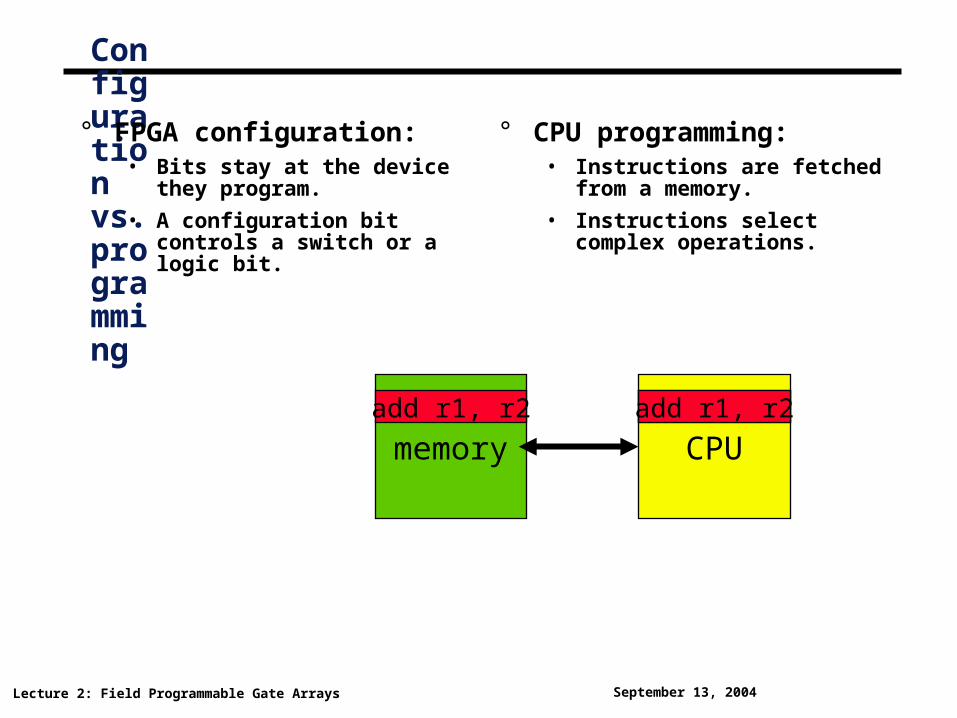
Configuration vs. programming
° FPGA configuration:• Bits stay at the device they
program.
• A configuration bit controls a switch or a logic bit.
° CPU programming:• Instructions are fetched from a
memory.
• Instructions select complex operations.
CPUmemoryadd r1, r2 IRadd r1, r2
Lecture 2: Field Programmable Gate Arrays September 13, 2004
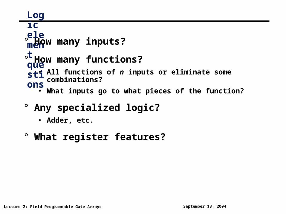
Logic element questions
° How many inputs?
° How many functions?• All functions of n inputs or eliminate some combinations?
• What inputs go to what pieces of the function?
° Any specialized logic?• Adder, etc.
° What register features?
Lecture 2: Field Programmable Gate Arrays September 13, 2004
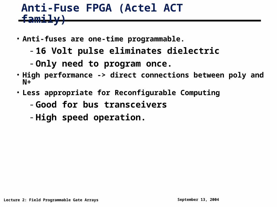
Anti-Fuse FPGA (Actel ACT family)
• Anti-fuses are one-time programmable.
- 16 Volt pulse eliminates dielectric
- Only need to program once.• High performance -> direct connections between poly and N+
• Less appropriate for Reconfigurable Computing
- Good for bus transceivers
- High speed operation.
Lecture 2: Field Programmable Gate Arrays September 13, 2004
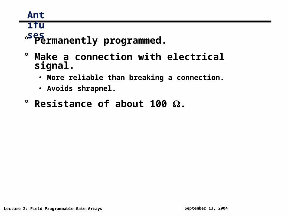
Antifuses° Permanently programmed.
° Make a connection with electrical signal.• More reliable than breaking a connection.
• Avoids shrapnel.
° Resistance of about 100 .
Lecture 2: Field Programmable Gate Arrays September 13, 2004
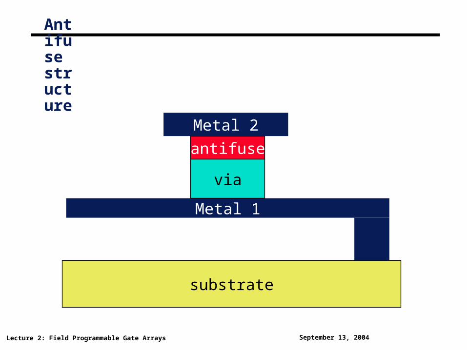
Antifuse structure
substrate
Metal 1
Metal 2
antifuse
via
Lecture 2: Field Programmable Gate Arrays September 13, 2004
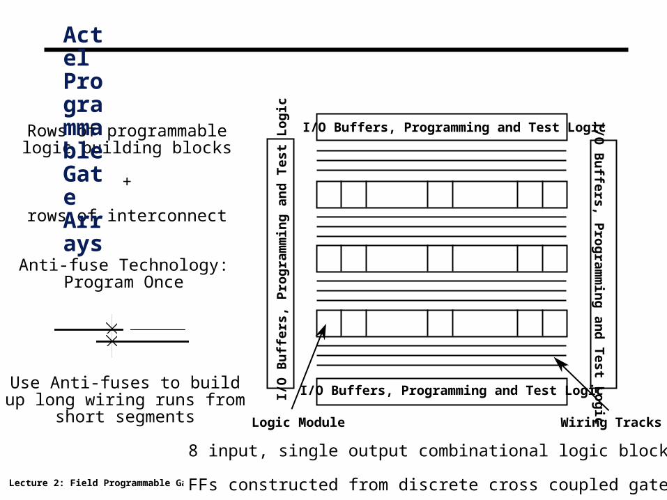
Rows of programmablelogic building blocks
+
rows of interconnect
Anti-fuse Technology:Program Once
8 input, single output combinational logic blocks
FFs constructed from discrete cross coupled gates
Use Anti-fuses to buildup long wiring runs from
short segments
I/O Buffers, Programming and Test Logic
Logic Module Wiring Tracks
I/O Buffers, Programming and Test Logic
I/O
Bu
ffer
s, P
rog
ram
min
g a
nd
Tes
t L
og
ic
I/O B
uffers, P
rog
ramm
ing
and
Test L
og
ic
Actel Programmable Gate Arrays
Lecture 2: Field Programmable Gate Arrays September 13, 2004
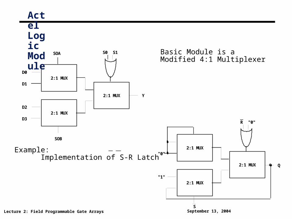
Basic Module is aModified 4:1 Multiplexer
Example: Implementation of S-R Latch
2:1 MUXD0
D1
SOA
2:1 MUXD2
D3
SOB
2:1 MUX
S0
Y
S1
2:1 MUX"0"
R
2:1 MUX"1"
S
2:1 MUX Q
"0"
Actel Logic Module
Lecture 2: Field Programmable Gate Arrays September 13, 2004
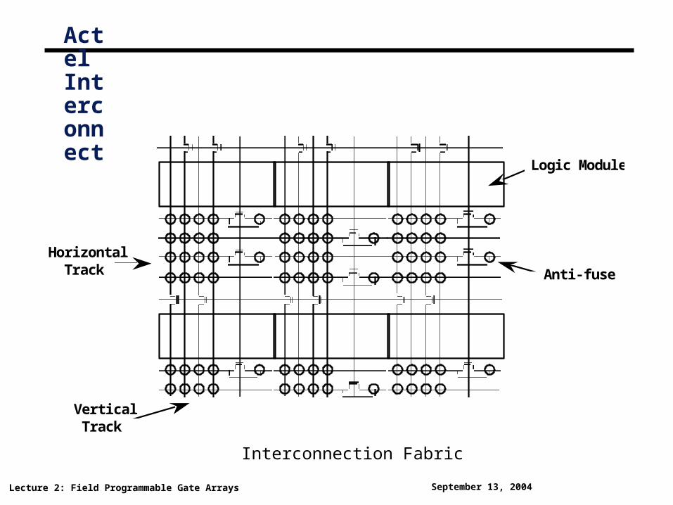
Interconnection Fabric
Logic Module
Horizontal Track
Vertical Track
Anti-fuse
Actel Interconnect
Lecture 2: Field Programmable Gate Arrays September 13, 2004
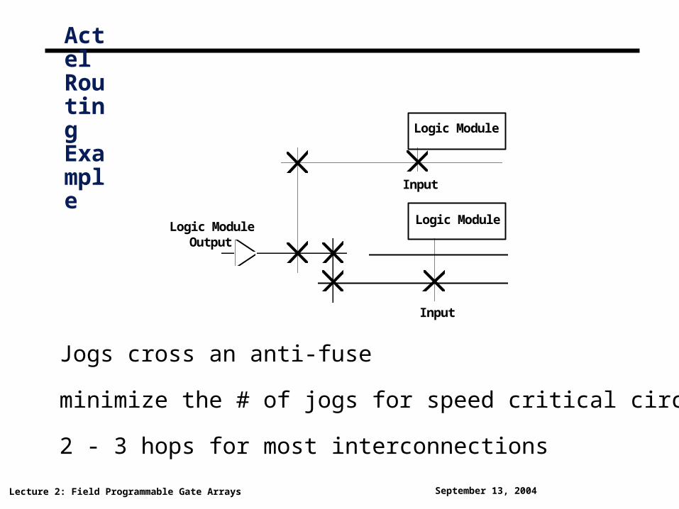
Jogs cross an anti-fuse
minimize the # of jogs for speed critical circuits
2 - 3 hops for most interconnections
Logic Module
Logic ModuleLogic Module Output
Input
Input
Actel Routing Example
Lecture 2: Field Programmable Gate Arrays September 13, 2004
EEPROM Devices (PLDs)
• Frequently used technology for PALs, GALs, EPLDs
• User design frequently decomposed into SOP representation
• Appropriate for system glue logic.
• Single transistor interconnection point.
Lecture 2: Field Programmable Gate Arrays September 13, 2004
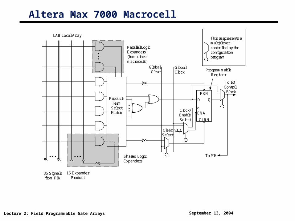
Altera Max 7000 Macrocell
Product-TermSelectMatrix
ClearSelect
Clock/EnableSelect
VCC
PRN
CLRN
ENA
D Q
GlobalClear
GlobalClock
To I/OControl
Block
To PIA
This respresents amultiplexercontrolled by theconfigurationprogram
ProgrammableRegister
36 Signalsfrom PIA
16 ExpanderProduct
Shared LogicExpanders
LAB Local Array
Parallel LogicExpanders(from othermacrocells)
Lecture 2: Field Programmable Gate Arrays September 13, 2004
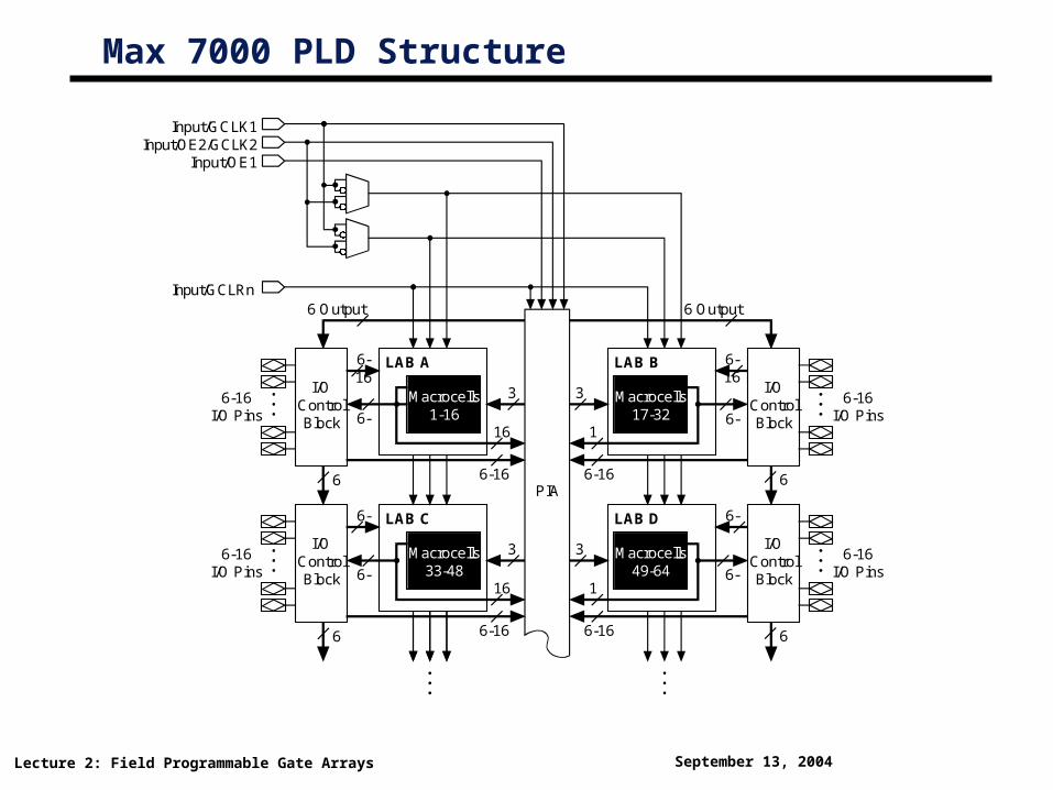
Max 7000 PLD Structure
Input/GCLK1Input/OE2/GCLK2
Input/OE1
LAB A
Macrocells1-166-
6-16
16
6-16
I/OControlBlock
6-16I/O Pins
3
LAB C
Macrocells33-486-
6-16
16
6-
I/OControlBlock
6-16I/O Pins
3
LAB B
LAB D
Macrocells17-32
Macrocells49-64
6-16
1
3
6-16
1
3
6-16I/O Pins
6-16I/O Pins
I/OControlBlock
I/OControlBlock
6
6
6
6
PIA
6 OutputInput/GCLRn
6 Output
6-
6-16
6-
6-
Lecture 2: Field Programmable Gate Arrays September 13, 2004
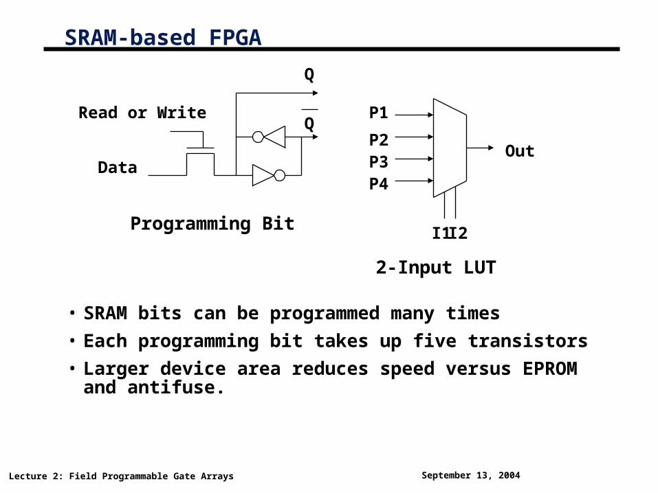
SRAM-based FPGA
• SRAM bits can be programmed many times
• Each programming bit takes up five transistors
• Larger device area reduces speed versus EPROM and antifuse.
Read or Write
Data
Q
Q
Programming Bit I1I2
P1
P2P3P4
Out
2-Input LUT
Lecture 2: Field Programmable Gate Arrays September 13, 2004
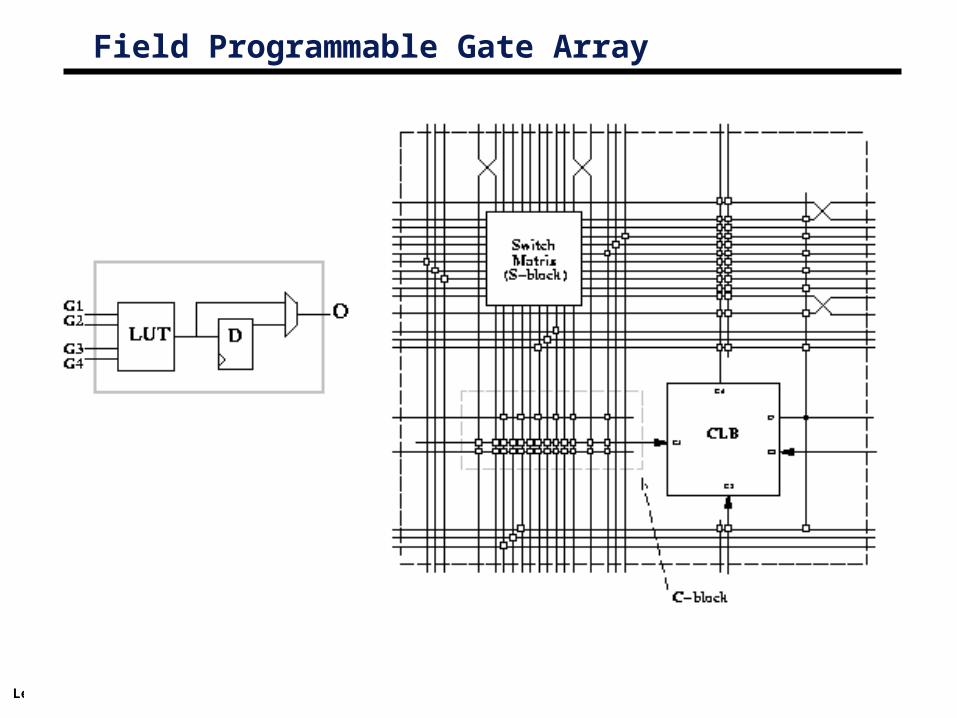
Field Programmable Gate Array
Lecture 2: Field Programmable Gate Arrays September 13, 2004
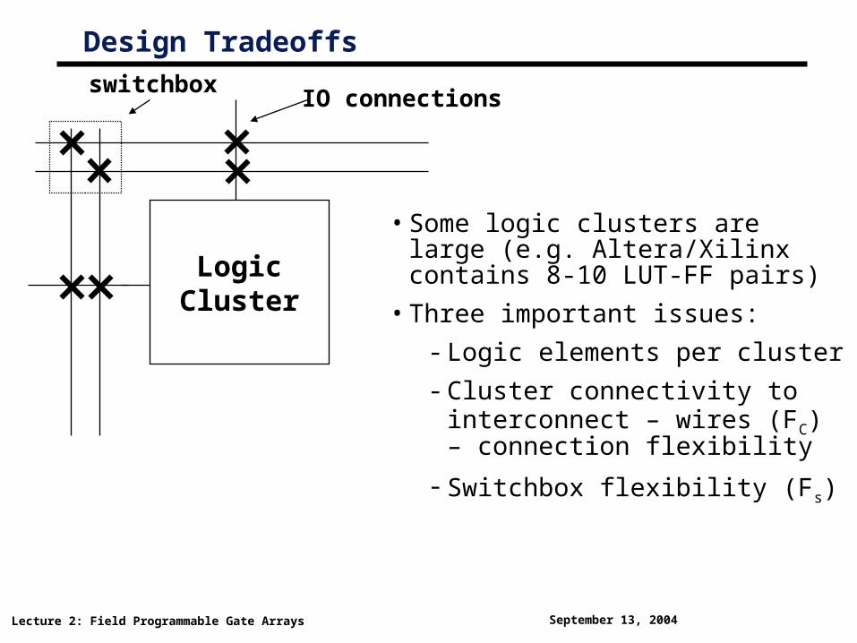
Design Tradeoffs
• Some logic clusters are large (e.g. Altera/Xilinx contains 8-10 LUT-FF pairs)
• Three important issues:
- Logic elements per cluster
- Cluster connectivity to interconnect – wires (FC) – connection flexibility
- Switchbox flexibility (Fs)
LogicCluster
IO connectionsswitchbox
Lecture 2: Field Programmable Gate Arrays September 13, 2004
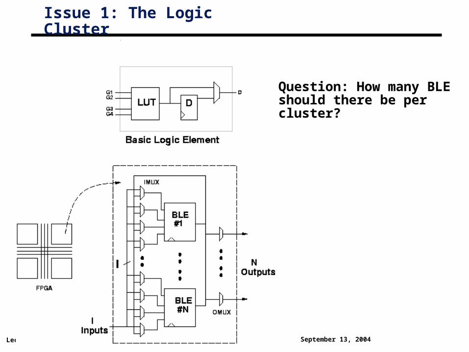
Issue 1: The Logic Cluster
• Question: How many BLE should there be per cluster?
Lecture 2: Field Programmable Gate Arrays September 13, 2004
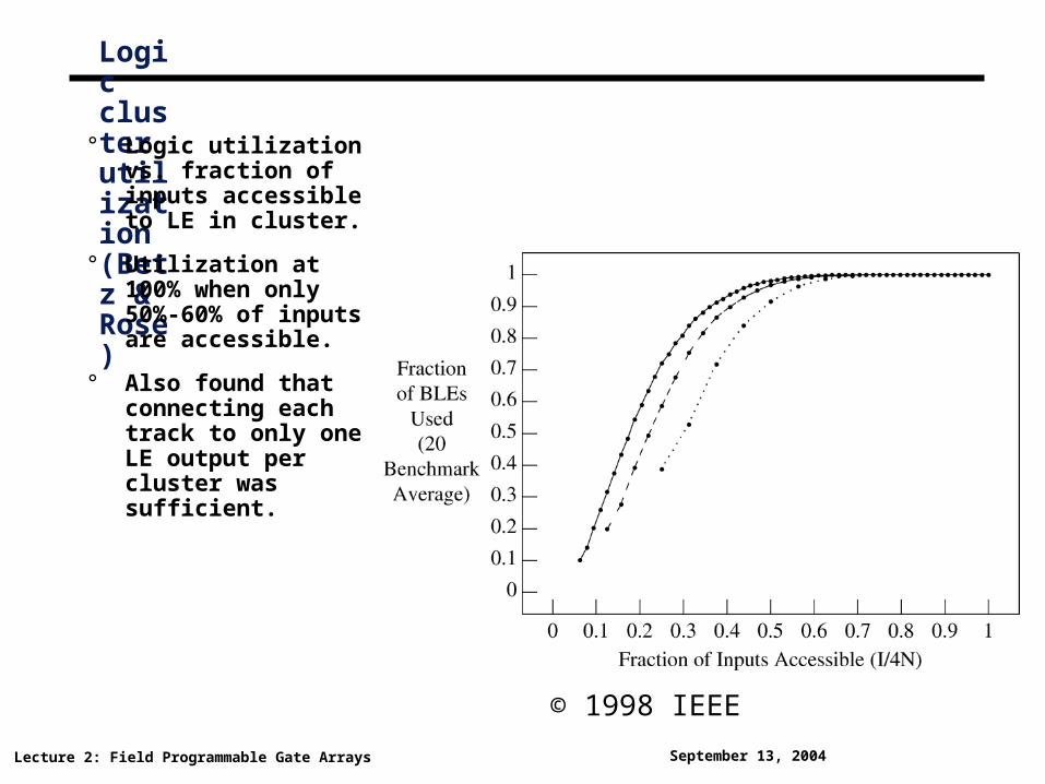
Logic cluster utilization (Betz & Rose)
° Logic utilization vs. fraction of inputs accessible to LE in cluster.
° Utilization at 100% when only 50%-60% of inputs are accessible.
° Also found that connecting each track to only one LE output per cluster was sufficient.
© 1998 IEEE
Lecture 2: Field Programmable Gate Arrays September 13, 2004
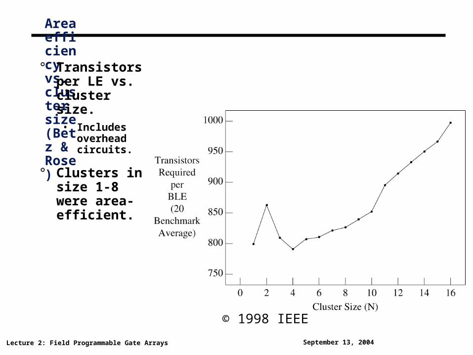
Area efficiency vs. cluster size (Betz & Rose)
° Transistors per LE vs. cluster size.
• Includes overhead circuits.
° Clusters in size 1-8 were area-efficient.
© 1998 IEEE
Lecture 2: Field Programmable Gate Arrays September 13, 2004
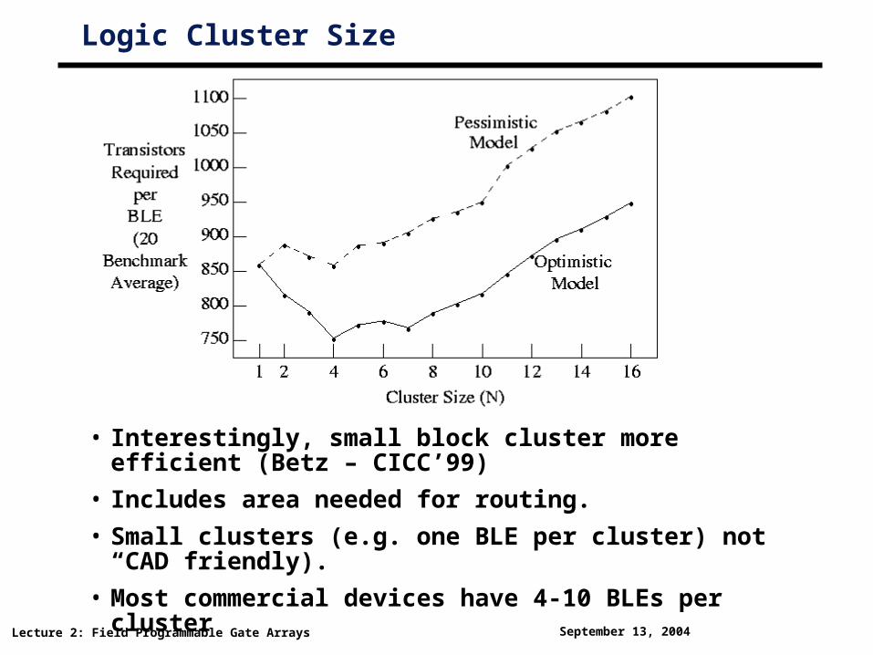
Logic Cluster Size
• Interestingly, small block cluster more efficient (Betz – CICC’99)
• Includes area needed for routing.
• Small clusters (e.g. one BLE per cluster) not “CAD friendly).
• Most commercial devices have 4-10 BLEs per cluster
Lecture 2: Field Programmable Gate Arrays September 13, 2004
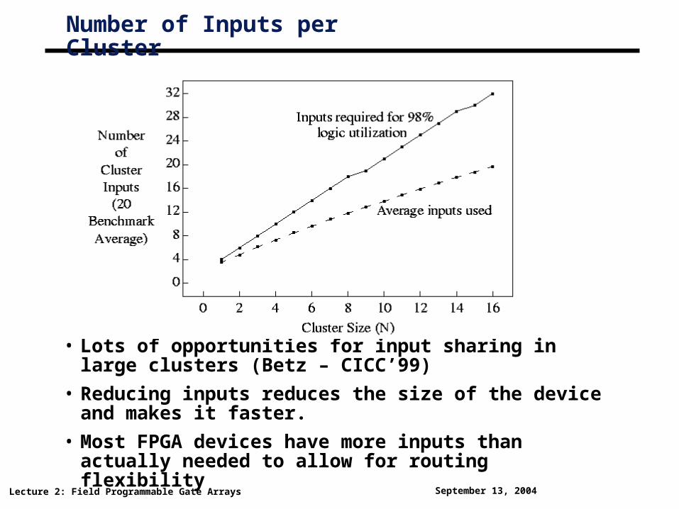
Number of Inputs per Cluster
• Lots of opportunities for input sharing in large clusters (Betz – CICC’99)
• Reducing inputs reduces the size of the device and makes it faster.
• Most FPGA devices have more inputs than actually needed to allow for routing flexibility
Lecture 2: Field Programmable Gate Arrays September 13, 2004
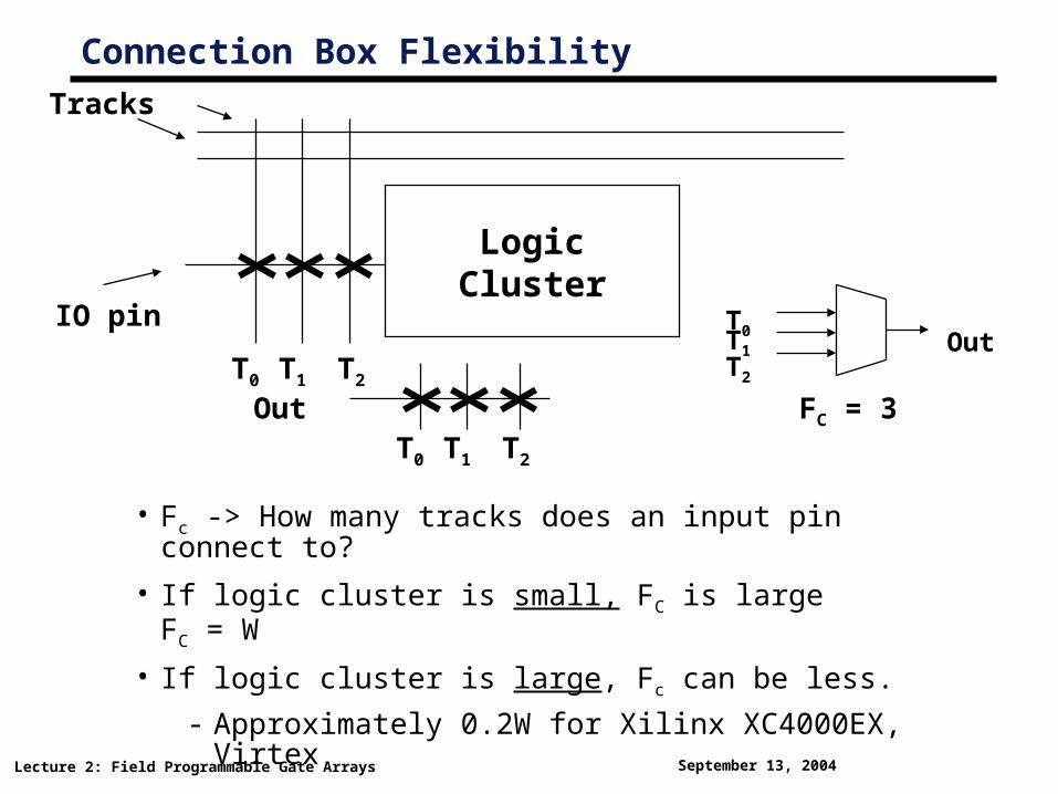
Connection Box Flexibility
• Fc -> How many tracks does an input pin connect to?
• If logic cluster is small, FC is large FC = W
• If logic cluster is large, Fc can be less.
- Approximately 0.2W for Xilinx XC4000EX, Virtex
LogicCluster
IO pin
Tracks
OutT0 T1 T2
T0T1T2
Out
FC = 3T0 T1 T2
Lecture 2: Field Programmable Gate Arrays September 13, 2004
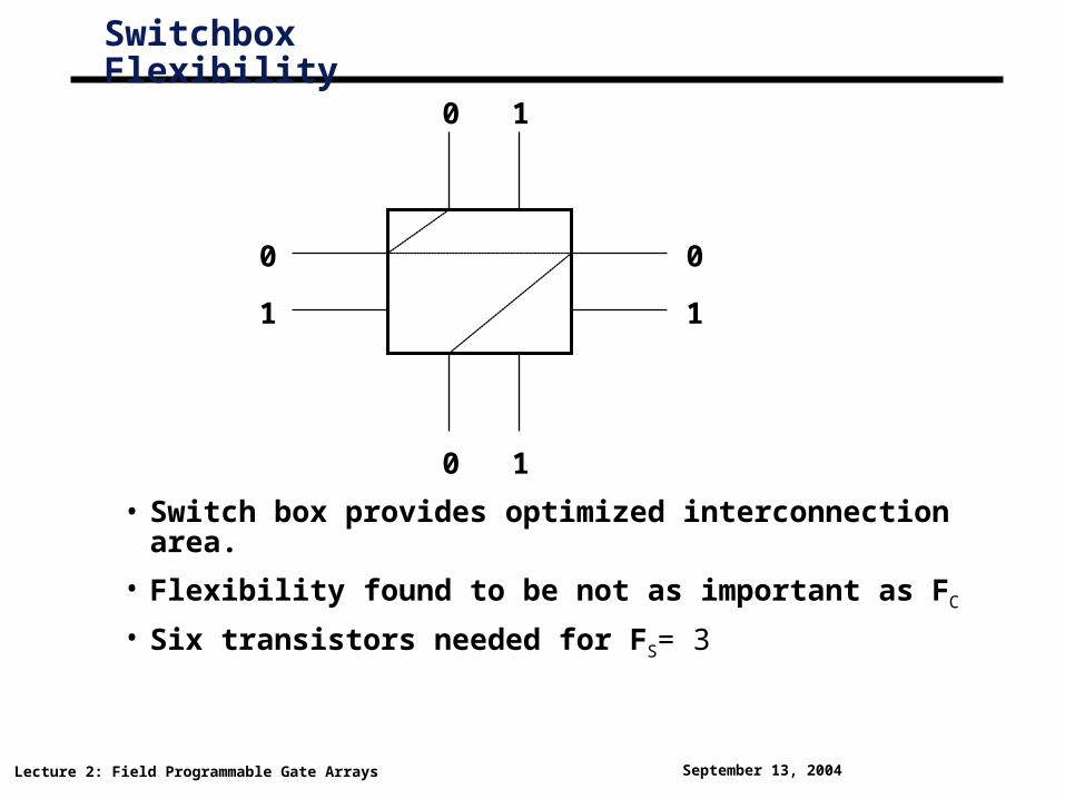
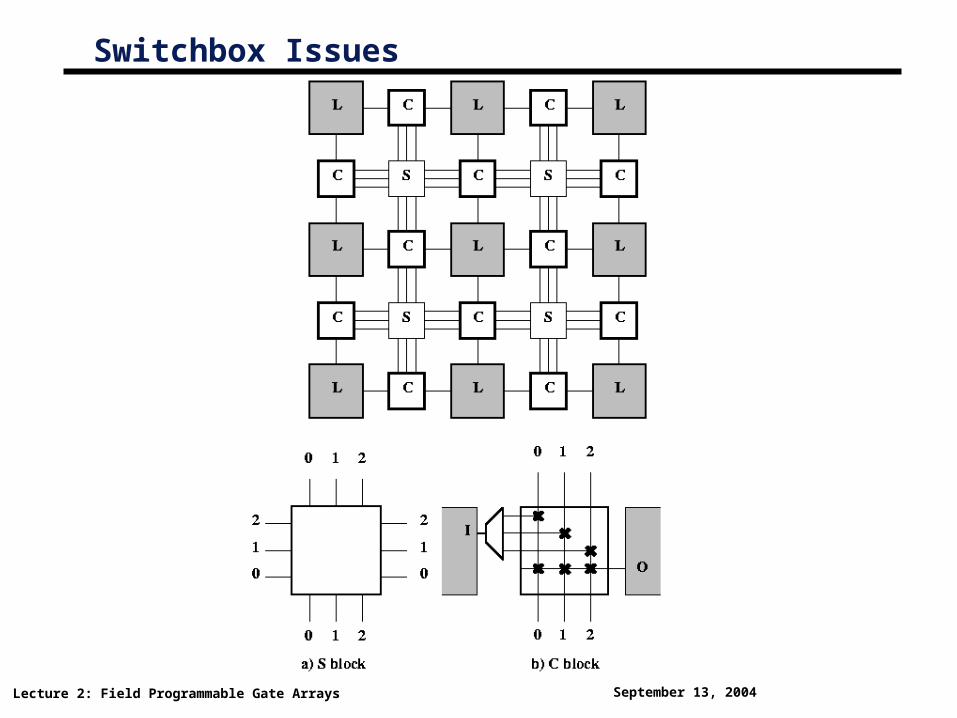
Switchbox Flexibility
• Switch box provides optimized interconnection area.
• Flexibility found to be not as important as FC
• Six transistors needed for FS= 3
0
1
0
1
0 1
0 1

Lecture 2: Field Programmable Gate Arrays September 13, 2004
Putting it all together
• Xilinx XC4000EX family
- FS = 3
- FC = 0.2
- I = 8• Altera Flex10K family
- FS = 3
- FC = 0.25
- I = 22
More contemporary FPGAs have larger cluster sizes and segmentation.• More difficult to quantify exact Fc and Fs values.
Lecture 2: Field Programmable Gate Arrays September 13, 2004
Switchbox Issues
Lecture 2: Field Programmable Gate Arrays September 13, 2004
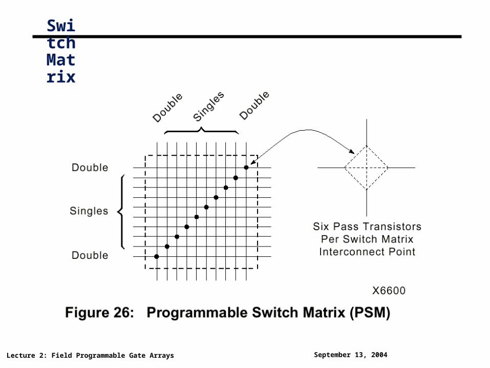
Switch Matrix
Lecture 2: Field Programmable Gate Arrays September 13, 2004
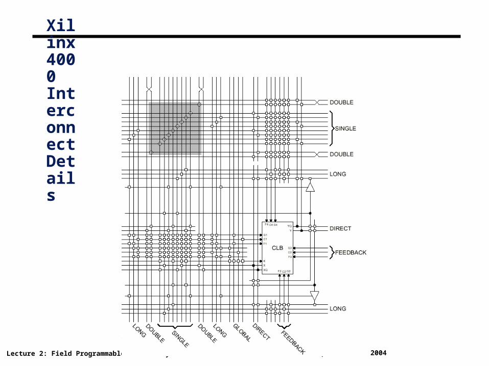
Xilinx 4000 Interconnect Details
Lecture 2: Field Programmable Gate Arrays September 13, 2004
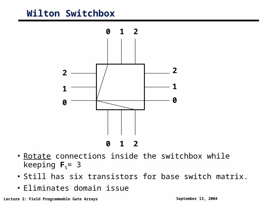
Wilton Switchbox
• Rotate connections inside the switchbox while keeping FS= 3
• Still has six transistors for base switch matrix.
• Eliminates domain issue
0 21
2
0
1
2
0
1
0 21

Lecture 2: Field Programmable Gate Arrays September 13, 2004
Switchbox Issues
Lecture 2: Field Programmable Gate Arrays September 13, 2004
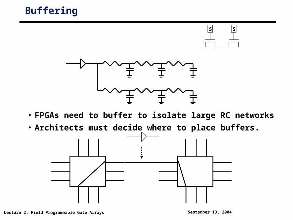
Buffering
• FPGAs need to buffer to isolate large RC networks
• Architects must decide where to place buffers.
S S
Lecture 2: Field Programmable Gate Arrays September 13, 2004
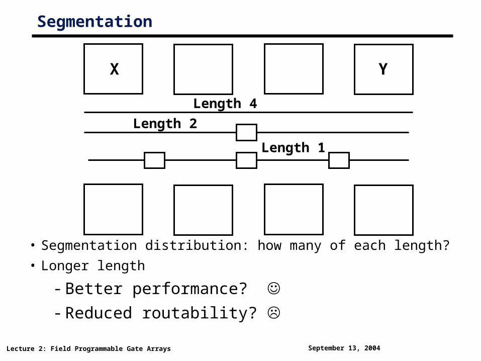
Segmentation
• Segmentation distribution: how many of each length?
• Longer length
- Better performance? - Reduced routability?
X Y
Length 4
Length 2
Length 1
Lecture 2: Field Programmable Gate Arrays September 13, 2004
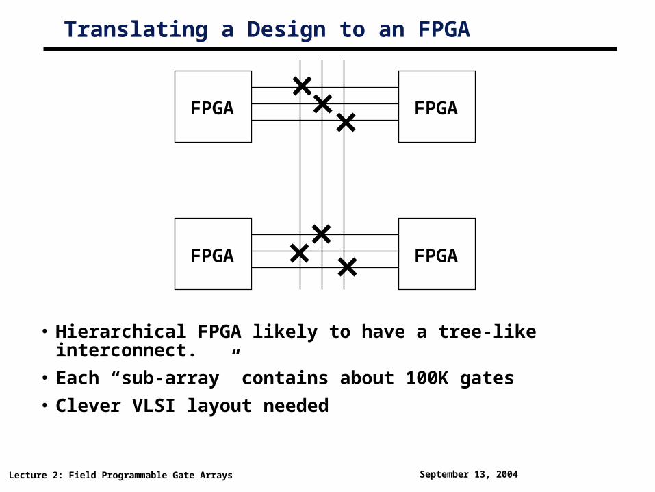
Translating a Design to an FPGA
• Hierarchical FPGA likely to have a tree-like interconnect.
• Each “sub-array” contains about 100K gates
• Clever VLSI layout needed
FPGA
FPGA
FPGA
FPGA
Lecture 2: Field Programmable Gate Arrays September 13, 2004
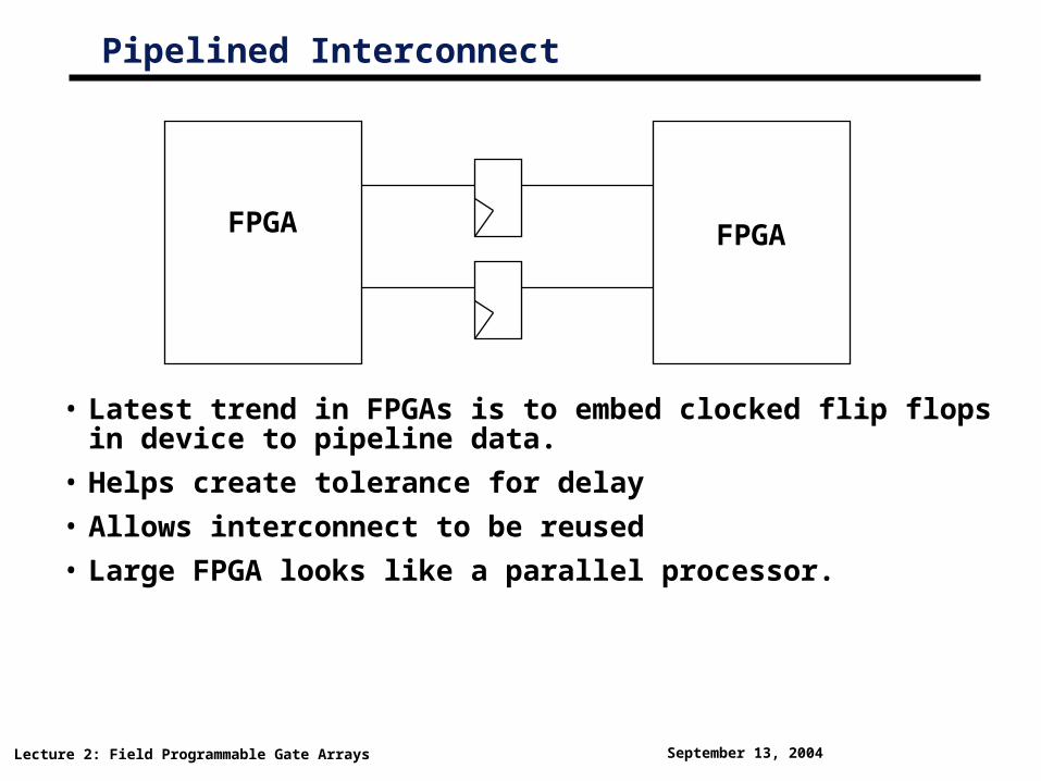
Pipelined Interconnect
• Latest trend in FPGAs is to embed clocked flip flops in device to pipeline data.
• Helps create tolerance for delay
• Allows interconnect to be reused
• Large FPGA looks like a parallel processor.
FPGA FPGA
Lecture 2: Field Programmable Gate Arrays September 13, 2004
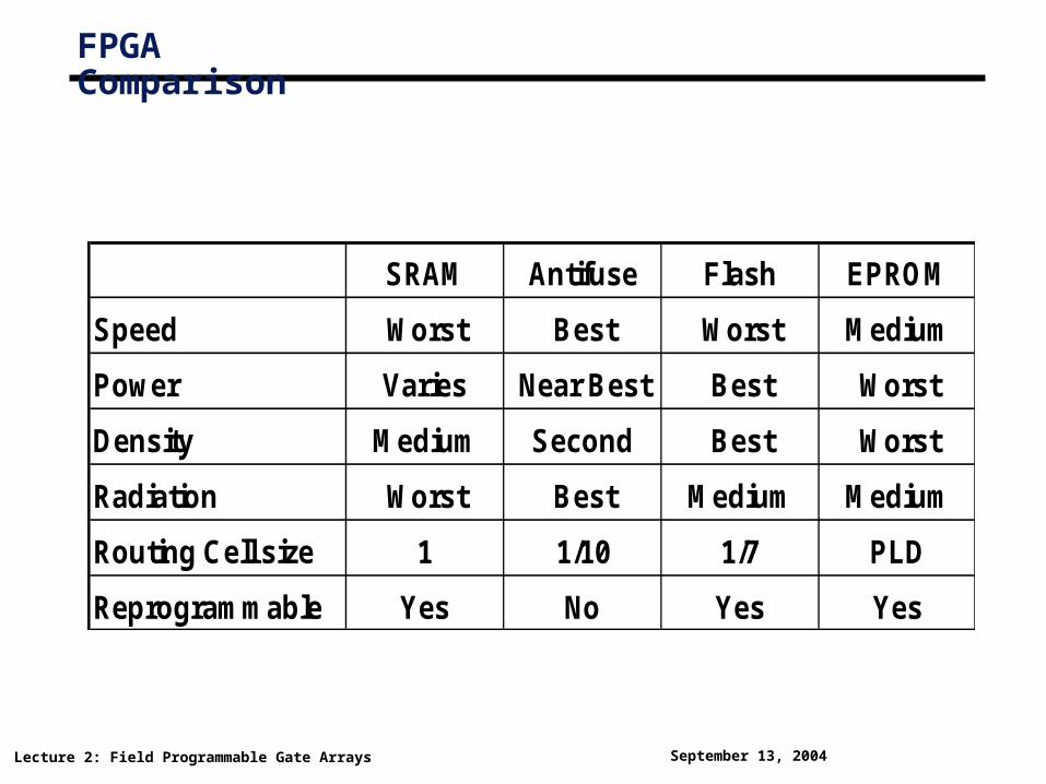
FPGA Comparison
SRAM Antifuse Flash EPROM
Speed Worst Best Worst Medium
Power Varies Near Best Best Worst
Density Medium Second Best Worst
Radiation Worst Best Medium Medium
Routing Cell size 1 1/10 1/7 PLD
Reprogrammable Yes No Yes Yes
Lecture 2: Field Programmable Gate Arrays September 13, 2004
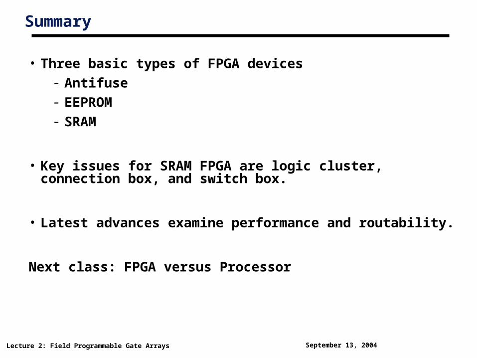
Summary
• Three basic types of FPGA devices
- Antifuse
- EEPROM
- SRAM
• Key issues for SRAM FPGA are logic cluster, connection box, and switch box.
• Latest advances examine performance and routability.
Next class: FPGA versus Processor


![Field Programmable Gate Arrays [Fpga]](https://img.pdfslide.net/doc/110x75/544092dcb1af9f441d8b45c9/field-programmable-gate-arrays-fpga.jpg)

