Embed Size (px)
Citation preview

Design of Computing SystemsRicardo Gutierrez-OsunaWright State University
Lecture 2: MC68000 interrupt in C language
g Problem definitiong Vectored interruptsg The vector tableg Introduction to the PI/Tg Basic PI/T operation g C language solution

Design of Computing SystemsRicardo Gutierrez-OsunaWright State University
Problem
g Setup the PI/T to read data from Port A and copy to Port B every 5 seconds
n Port A should be programmed for non-latched inputn Port B should be programmed for single-buffered outputn Timer should be setup to interrupt the MC68000 every 5 seconds
PortA
Timer
PI/TMC68000
PortB
Read
Write
Interrupt (5 s.)
Sensor data
Motor command

Design of Computing SystemsRicardo Gutierrez-OsunaWright State University
Vectored interrupts

Design of Computing SystemsRicardo Gutierrez-OsunaWright State University
Vectored interrupts
g The 68000 provides two interrupt schemesn Vectored: intended for modern 16-bit peripheralsn Auto-vectored: intended for older 8-bit peripherals
g There are seven levels of interrupts availableg The sequence of operations during a vectored interrupt request is the following
n A peripheral requires attention by asserting its interrupt request output (IRQ*)n The priority encoder produces a 3-bit code with the highest IRQ* line active and passes it to
the 68000 on the IPL0*-IPL3* inputsn The 68000 compares the level of the interrupt with the interrupt mask flag (I2I1I0) in the SR. n If the requested input is greater than (I2I1I0), the interrupt is serviced, otherwise it is ignoredn If the 698000 decides to service the interrupt:
g The code 111 is placed on (FC2FC1FC0) to inform the system that an interrupt is about to be servicedg The priority of the interrupt is placed on (A3A2A1)g (FC2FC1FC0) and (A3A2A1) are passed to an interrupt acknowledge decoder which asserts one of the
seven IACK* lines
n The asserted IACK* line informs the interrupting device that it is about to be servicedn The peripheral whose interrupt level matches the asserted IACK* will “know” that it is going
to be servicedn The peripheral then writes the IVEC vector onto the data bus (D7D0) and asserts the
DTACK* line (DTACK stands for Data Transfer Acknowledge)n the active DTACK* terminates the IACK cycle and the 68000 will execute the interrupt
handler pointed by the vector fetched from (D7D0)

Design of Computing SystemsRicardo Gutierrez-OsunaWright State University
The vector table

Design of Computing SystemsRicardo Gutierrez-OsunaWright State University
Introduction to the 68230
g The 68230 PI/T (Parallel Interface/Timer) is a general-purpose peripheral
n Its primary function is a parallel interfacen Its secondary function is a programmable timer
g The PARALLEL INTERFACE provides 4 modes with various handshaking and buffering capabilities
n Unidirectional 8-bitn Unidirectional 16-bitn Bidirectional 8-bit n Bidirectional 16-bit
g The PROGRAMMABLE TIMER provides a variety of OS servicesn Periodic interrupt generationn Square wave generationn Interrupt after timeoutn Elapsed time measurementn System watchdog

Design of Computing SystemsRicardo Gutierrez-OsunaWright State University
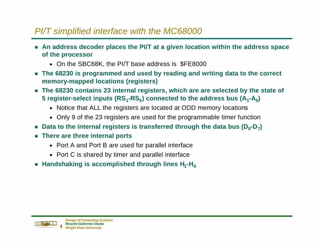
PI/T simplified interface with the MC68000
Design of Computing SystemsRicardo Gutierrez-OsunaWright State University
PI/T simplified interface with the MC68000
g An address decoder places the PI/T at a given location within the address space of the processor
n On the SBC68K, the PI/T base address is $FE8000g The 68230 is programmed and used by reading and writing data to the correct
memory-mapped locations (registers)g The 68230 contains 23 internal registers, which are are selected by the state of
5 register-select inputs (RS1-RS5) connected to the address bus (A1-A5)n Notice that ALL the registers are located at ODD memory locationsn Only 9 of the 23 registers are used for the programmable timer function
g Data to the internal registers is transferred through the data bus (D0-D7)g There are three internal ports
n Port A and Port B are used for parallel interfacen Port C is shared by timer and parallel interface
g Handshaking is accomplished through lines H1-H4

Design of Computing SystemsRicardo Gutierrez-OsunaWright State University
PI/T timer registersg Timer Control Register (TCR)
n Determines the operation modes of the timer
g Timer Interrupt Vector Register (TIVR)n Stores the interrupt vector number
g Counter Preload Register (CPR)n A 24-bit counter with the desired (by the
programmer) number of counts measured in ticks
g Counter Register (CNTR)n A 24-bit counter down-counter that is
automatically decremented with every tick
g Timer Status Register (TSR)n Determines the status of the timern Only Bit #0 (Zero Detect Status or ZDS) is usedn In order to clear the ZDS bit after a zero-detect
YOU MUST WRITE A 1 to it (YES, the ZDS bit is cleared by writing a ONE to it)
Register and Mnemonic Acc. OffsetTimer Control Register TCR R/W $21Timer Interrupt Vector Register TIVR R/W $23Counter Preload Register High CPRH R/W $27Counter Preload Register Middle CPRM R/W $29Counter Preload Register Low CPRL R/W $31Counter Register High CNTRH R $2FCounter Register Middle CNTRM R $31Counter Register Low CNTRL R $33Timer Status Register TSR R/W $35

Design of Computing SystemsRicardo Gutierrez-OsunaWright State University
Timer Control Register
g Timer Enable (TCR0)n Turns the timer ON and OFF. The timer is disabled when the bit is cleared; it is enabled when set
g To start the timer, place an 1 in TCR0
g To stop the timer, place a 0 in TCR0
g Clock Control (TCR1-2)n The PI/T timer permits different clock pulse operations. When the field is 00, every 32 CPU clock cycles
become 1 timer tick.
g Counter Load (TCR4)n After completing its countdown, the tick counter is either reset from the Counter Preload Register (CPR) or it
rolls over to $FFFFFFg Writing a 0 on TCR4 causes a reload from the CPRg Writing a 1 on TCR4 causes a roll-over to $FFFFFF.
g Action on Zero Detect (TCR5-7)n The timer can select from a series of actions when the tick counter reaches 0.
Mode TCR7 TCR6 TCR5 TCR4 TCR3 TCR2 TCR1 TCR01 1 X 1 0 X 00 or 1X 12 0 1 X 0 X 00 or 1X 13 1 X 1 1 X 00 or 1X 14 0 0 X 1 X 0 0 15 0 0 X 1 X 0 X 16 1 X 1 1 X 0 1 1
TOUT/TIACK* control ZDcontrol
Notused Clock control Timer
enableMode 1: Real-time clockMode 2: Square wave generatorMode 3: Interrupt after timeout
Mode 4: Elapsed time measurementMode 5: Pulse counterMode 6: Period measurement

Design of Computing SystemsRicardo Gutierrez-OsunaWright State University
Clock control (TCR2-TCR1)
g The counter can be decremented from three different signalsn TIN, the external clock inputn The output of a 5-bit prescaler driven by CLK and enabled by TIN
n CLK, the system clock (prescaled)
g The 5-bit prescaler allows us to divide the counter frequency by 32g The SBC68K clock runs at 8MHz (125×10-9 seconds per count), so 1 second will require
250,000 CLK ticks (mode 00)
TCR2 TCR1 Clock Control Example
0 0PC2/TIN is a port C function. The counter clock is prescaled by 32, thus
the counter clock is CLK/32. The timer enable bit determines whether thetimer is in the run or halt state.
Prescaler CounterCLK
0 1
PC2/T IN is a timer input. The prescaler is decremented on the falling edgeof CLK and the counter is decremented when the prescaler rolls over
from $00 to $1F (3110) Timer is in the run state when BOTH timer enablebit and TIN are asserted.
Prescaler CounterCLK
TIN
1 0
PC2/T IN is a timer input and is prescaled by 32. The prescaler isdecremented following the rising transition of TIN after being
synchronized with the internal clock. The 24-bit counter is decrementedwhen the prescaler rolls over from $00 to $1F. The timer enable bit
determines whether the timer is in the run or halt state.
Prescaler CounterTIN
1 1
PC2/TIN is a timer input and prescaling is not used. The 24-bit counter isdecremented following the rising edge of the signal at the TIN pin after
being synchronized with the internal clock. The timer enable bitdetermines whether the timer is in the run or halt state.
TIN Counter

Design of Computing SystemsRicardo Gutierrez-OsunaWright State University
TOUT/TIACK* control (TCR7-TCR5)
g Bits 7-5 of the Timer Control Register control the way the PI/T timer behaves on a zero-detect (ZDS=1)
n Whether interrupts are supported (vectored, auto-vectored or none)n How does the PC3/TOUT output pin behaven How is the PC7/TIACK* input pin interpreted
TCR7 TCR6 TCR5Timer response
(simplified) Timer response (detailed)
0 0 X Use timer pins for theoperation of I/O port C PC3/TOUT and PC7/TIACK* are port C functions
0 1 XToggle a square wavewith each expiration of
the timer
PC3/TOUT is a timer function. In the run state TOUT provides a square wave whichis toggled on each zero-detect. The TOUT pin is high in the halt state. PC7/TIACK*
is a port C function.
1 0 0 No vectored interruptgenerated on a count of 0
PC3/TOUT is a timer function. In the run or halt state TOUT is used as a timerrequest output. Timer interrupt is disabled, the pin is always three-stated.PC7/TIACK* is a port C function. Since interrupt requests are negated, PI/T
produces no response to an asserted TIACK*.
1 0 1 Generate a vectoredinterrupt on a count of 0
PC3/T OUT is a timer function and is used as a timer interrupt request output. Thetimer interrupt is enabled and TOUT is low (IRQ* asserted) whenever the ZDS bit
is set. PC7/TIACK* is used to detect the 68000 IACK cycle. This combinationoperates in the vectored-interrupt mode.
1 1 0No autovectored
interrupt generated on acount of 0
PC3/T OUT is a timer function. In the run or halt state it is used as a timer interruptrequest output. The timer interrupt is disabled and the pin always three-stated.
PC7/TIACK* is a port C function.
1 1 1Generate an auto-
vectored interrupt on acount of 0
PC3/T OUT is a timer function and is used as a timer interrupt request output. Thetimer interrupt is enabled and TOUT is low whenever the ZDS bit is set.
PC7/TIACK* is a port C function. This combination operates in an autovectoredinterrupt mode.
Design of Computing SystemsRicardo Gutierrez-OsunaWright State University
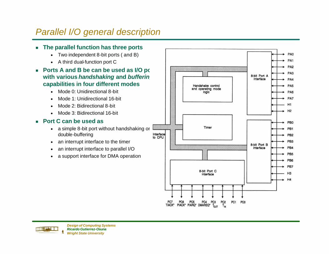
Parallel I/O general description
g The parallel function has three portsn Two independent 8-bit ports ( and B)n A third dual-function port C
g Ports A and B be can be used as I/O ports with various handshaking and buffering capabilities in four different modes
n Mode 0: Unidirectional 8-bitn Mode 1: Unidirectional 16-bitn Mode 2: Bidirectional 8-bitn Mode 3: Bidirectional 16-bit
g Port C can be used asn a simple 8-bit port without handshaking or
double-bufferingn an interrupt interface to the timer n an interrupt interface to parallel I/On a support interface for DMA operation
Design of Computing SystemsRicardo Gutierrez-OsunaWright State University
Brief overview of parallel I/O registers
g Port General Control Register (PGCR)n Selection of I/O modes (0, 1, 2 and 3) and handshaking signals (H1, H2, H3 and H4)
g Port Service Request Register (PSSR)n Selection of Port C functions: DMA requests, IRQ/IACK signals and handshaking signal
priority
g Port {A,B,C} Data Direction Register (PxDDR)n Selection of individual port bits as inputs or outputs
g Port Interrupt Vector Register (PIVR)n Storage of vector number for vectored interrupts
g Port {A,B} Control Register (PxCR)n Selection of port sub-modes and handshake signals operation
g Port {A,B,C} Data Register (PxDR)n Contents of the I/O ports
g Port {A,B} Alternate Data Register (PxADR)n Instantaneous logic levels of the I/O pins of the port
g Port Status Register (PSR)n Status information of the handshake signals

Design of Computing SystemsRicardo Gutierrez-OsunaWright State University
The PI/T’s modes of operation
H2(H4)H1(H3)
A(B) [8]
MC
6823
0
H2(H4)H1(H3)
A(B) [8]
MC
6823
0
H2(H4)H1(H3)
A(B) [8]
MC
6823
0
H4H3
A+B [16]
MC
6823
0
H2H1
H4H3
A+B [16]
MC
6823
0H2H1
H4H3
MC
6823
0
H2H1
B [8]
A [8]
Output Xfers
Input XfersH4H3
MC
6823
0
H2H1
A+B [16]
Output Xfers
Input Xfers
Mode 0 (1D/8bit) Mode 1 (1D/16bit) Mode 2 (2D/8bit) Mode 3 (2D/16bit)
Sub
-mo
de
00S
ub-m
od
e 01
Sub
-mo
de
1X
Sub
-mod
e X
0S
ub-m
ode
X1
NPd*
Unidirectional
Single-buffered
Non-latched
LEGEND
*NPd: This is the ONLY mode that is Not Pin-definable
Double-buffered
Bidirectional
Design of Computing SystemsRicardo Gutierrez-OsunaWright State University
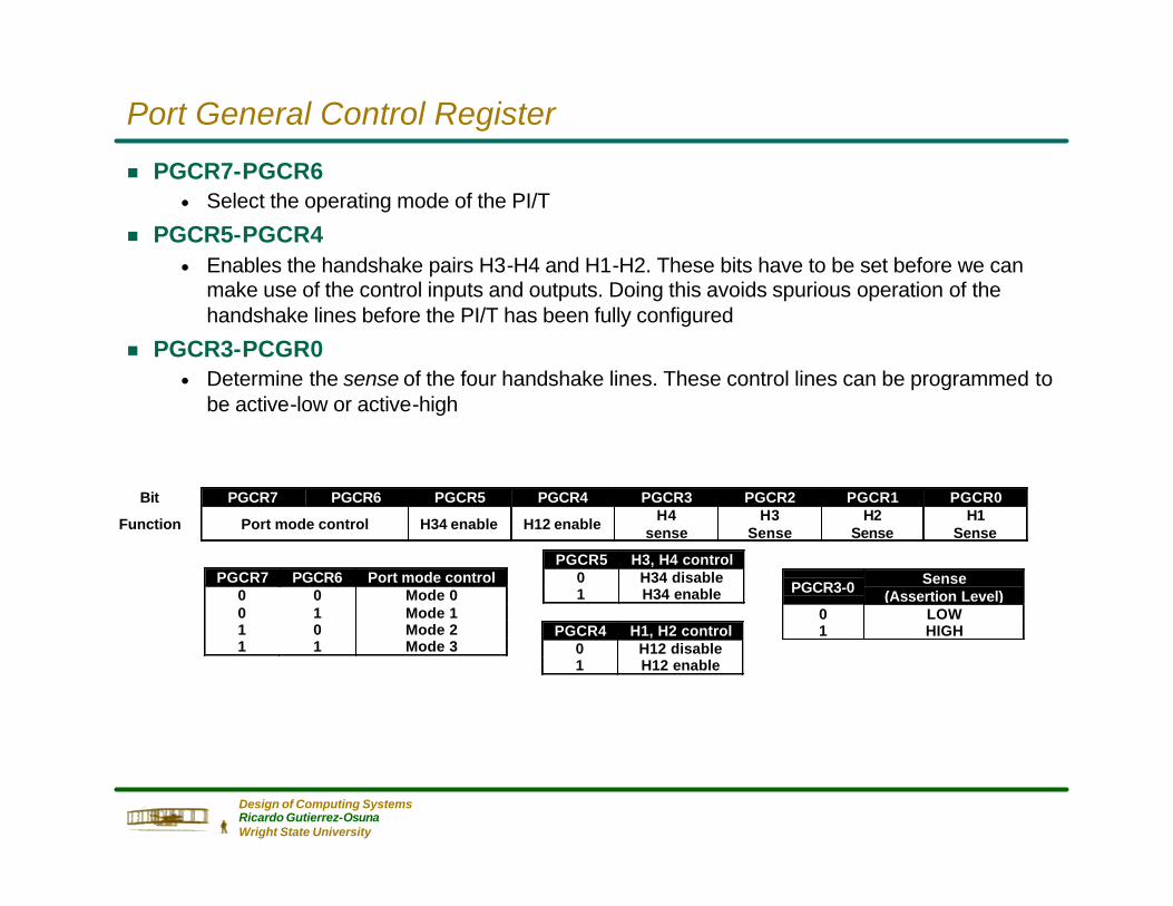
Port General Control Register
g PGCR7-PGCR6n Select the operating mode of the PI/T
g PGCR5-PGCR4n Enables the handshake pairs H3-H4 and H1-H2. These bits have to be set before we can
make use of the control inputs and outputs. Doing this avoids spurious operation of the handshake lines before the PI/T has been fully configured
g PGCR3-PCGR0n Determine the sense of the four handshake lines. These control lines can be programmed to
be active-low or active-high
Bit PGCR7 PGCR6 PGCR5 PGCR4 PGCR3 PGCR2 PGCR1 PGCR0
Function Port mode control H34 enable H12 enable H4sense
H3Sense
H2Sense
H1Sense
PGCR7 PGCR6 Port mode control0 0 Mode 00 1 Mode 11 0 Mode 21 1 Mode 3
PGCR5 H3, H4 control0 H34 disable1 H34 enable
PGCR4 H1, H2 control0 H12 disable1 H12 enable
PGCR3-0 Sense(Assertion Level)
0 LOW1 HIGH

Design of Computing SystemsRicardo Gutierrez-OsunaWright State University
Port Data Direction Registers
g Port Data Direction Registers: PADDR,PBDDR and PCDDRn Select the direction and buffering characteristics of each of the appropriate port pins
g A logical ONE makes the corresponding pin act as an OUTPUTg A logical ZERO makes the corresponding pin act as an INPUT
n Port C behaves in the same fashion and determines whether each dual-function chosen for port C operation is an input or an output
Bit PADDR7 PADDR6 PADDR5 PADDR4 PADDR3 PADDR2 PADDR1 PADDR0Function Bit 7 Bit 6 Bit 5 Bit 4 Bit 3 Bit 2 Bit 1 Bit 0
Bit PBDDR7 PBDDR6 PBDDR5 PBDDR4 PBDDR3 PBDDR2 PBDDR1 PBDDR0Function Bit 7 Bit 6 Bit 5 Bit 4 Bit 3 Bit 2 Bit 1 Bit 0
Bit PCDDR7 PCDDR6 PCDDR5 PCDDR4 PCDDR3 PCDDR2 PCDDR1 PCDDR0Function Bit 7 Bit 6 Bit 5 Bit 4 Bit 3 Bit 2 Bit 1 Bit 0

Design of Computing SystemsRicardo Gutierrez-OsunaWright State University
Port Service Request Register
g PSSR6-PSSR5 (service request)n Determines whether the PI/T generates an interrupt or a DMA request
g PSSR4-PSSR3 (operation select)n Determines whether two of the dual-function pins belong to port C or perform special-
purpose functions
g PSSR2-PSSR0 (interrupt-priority control)
Bit PSRR7 PSRR6 PSRR5 PSRR4 PSRR3 PSRR2 PSRR1 PSRR0
Function × SRVRQ(DMA control) Interrupt control Port interrupt priority
PSRR6 PSRR5 Interrupt pin function0 × PC4/DMAREQ* = PC4 DMA not used
1 0 PC4/DMAREQ* = DMAREQ* Associated with double-buffered transfers controlled by H1H1 does not cause interrups in this mode
1 1 PC4/DMAREQ* = DMAREQ* Associated with double-buffered transfers controlled by H3H3 does not cause interrups in this mode
PSRR4 PSRR3 Interrupt pin function
0 0 PC5/PIRQ* = PC5PC6/PIACK* = PC6
No interrupt supportNo interrupt support
0 1 PC5/PIRQ* = PIRQ*PC6/PIACK* = PC6
Autovectored interrupt supportedAutovectored interrupt supported
1 0 PC5/PIRQ* = PC5PC6/PIACK* = PIACK*
1 1 PC5/PIRQ* = PIRQ*PC6/PIACK* = PIACK*
Vectored interrupt supportedVectored interrupt supported
PSRR2 PSRR1 PSRR0Order of priority interruptHiguest ←→Lowest
0 0 0 H1S H2S H3S H4S0 0 1 H2S H1S H3S H4S0 1 0 H1S H2S H4S H3S0 1 1 H2S H1S H4S H3S1 0 0 H3S H4S H1S H2S1 0 1 H3S H4S H2S H1S1 1 0 H4S H3S H1S H2S1 1 1 H4S H3S H2S H1S

Design of Computing SystemsRicardo Gutierrez-OsunaWright State University
Mode 0, sub-mode 00
H2(H4)H1(H3)
A(B) [8]
MC
6823
0
g Data flown Double-buffered input orn Single-buffered output
g Applicationsn Normally used to receive data from devices such as A/D converters
g Handshakingn Data is latched into the input register by the asserted edge of H1n H2 behaves according to its programming function defined below
g Port B behaves identically (using H3 and H4)
Bit PACR7 PACR6 PACR5 PACR4 PACR3 PACR2 PACR1 PACR00 0 H2 Control H2 Int. H1 Control
←→Sub-mode 00
PACR5 PACR4 PACR3 H2 Control H2S0 X X Input pin: Edge-sensitive input Set on asserted edge1 0 0 Output pin: negated Always clear1 0 1 Output pin: asserted Always clear1 1 0 Output pin: interlocked input handshake Always clear1 1 1 Output pin: pulsed input handshake Always clear
PACR1 PACR0 H1 Control0 X H1 interrupt and DMA request disabled1 X H1 interrupt and DMA request enabled
X X H1S status set anytime data is availablein the double-buffered input path
PACR2 H2 interrupt0 H2 interrupt disabled1 H2 interrupt enabled

Design of Computing SystemsRicardo Gutierrez-OsunaWright State University
g Data flown Double-buffered output orn Non-latched input
g Applicationsn Normally used to send data to devices such as D/A converters or printers
g Tables are almost identical to 0/00 except for PACR0n If PACR0=0, H1S is set when port A is half-emptyn If PACR0=1, H1S is set when port A is full-empty
g Port B control is identical (using H3 and H4, of course)
H2(H4)H1(H3)
A(B) [8]
MC
6823
0
Bit PACR7 PACR6 PACR5 PACR4 PACR3 PACR2 PACR1 PACR00 1 H2 Control H2 Int. H1 Control
←→Sub-mode 01
PACR5 PACR4 PACR3 H2 Control H2S0 X X Input pin: Edge-sensitive input Set on asserted edge1 0 0 Output pin: negated Always clear1 0 1 Output pin: asserted Always clear1 1 0 Output pin: interlocked input handshake Always clear1 1 1 Output pin: pulsed input handshake Always clear
PACR2 H2 interrupt0 H2 interrupt disabled1 H2 interrupt enabled
PACR1 PACR0 H1 Control0 X H1 interrupt and DMA request disabled1 X H1 interrupt and DMA request enabled
X 0 H1S status set if either initial or final outputlatches can accept data and cleared otherwise
X 1 H1S status set if both initial and final outputlatches are empty and cleared otherwise
Mode 0, sub-mode 01

Design of Computing SystemsRicardo Gutierrez-OsunaWright State University
Solution
/* Timer Register Addresses */
#define tmr ((unsigned char*) 0xFE8021) /* Timer Base Address */#define tcr (( unsigned char*) tmr) /* Timer Control Reg */#define tivr (( unsigned char*) tmr+2) /* Timer Interrupt Vector Reg */ #define cprh (( unsigned char*) tmr+6) /* Preload Hi Reg */ #define cprm (( unsigned char*) tmr+8) /* Preload Mid Reg */ #define cprl (( unsigned char*) tmr+10) /* Preload Lo Reg */ #define cnrh (( unsigned char*) tmr+14) /* Counter Hi Reg */ #define cnrm (( unsigned char*) tmr+16) /* Counter Mid Reg */ #define cnrl (( unsigned char*) tmr+18) /* Counter Lo Reg */ #define tsr (( unsigned char*) tmr+20) /* Timer Status Reg */
/* Parallel I/O Register Addresses */
#define PGCR ( unsigned char*)0xFE8001 /* PI/T General Control Reg */#define PSRR ( unsigned char*)0xFE8003 /* PI/T Service Routine Reg */#define PIVR ( unsigned char*)0xFE800B /* PI/T Interrupt Vector Reg */#define PSR ( unsigned char*)0xFE801B /* PI/T Status Reg */#define PACR ( unsigned char*)0xFE800D /* PI/T Port A Control Reg */#define PADDR ( unsigned char*)0xFE8005 /* Port A Data Direction Reg */#define PADR ( unsigned char*)0xFE8011 /* Port A Data Reg */#define PBCR ( unsigned char*)0xFE800F /* Port B Control Reg */#define PBDDR ( unsigned char*)0xFE8007 /* Port B Data Direction Reg */#define PBDR ( unsigned char*)0xFE8013 /* Port B Data Reg */
void isr() {printf("Five secs has passed\n");
*pbdr = *padr ; /* This is really the main job of isr *It copies the content Port A data register (our input port)and then places it to Port B (our output port)*/
*tsr = 0x01; /* reset the ZDS bit */
asm(" rte");}
main () {long *vtable;int count=1250000;
asm(” move.w #$2400,SR");asm(” movea.l #$20000,SP);
*PGCR = 0x0F; /* disable Port A & B */*PADDR = 0x00; /* Set Port A as input */*PBDDR = 0xFF; /* set Port B as Output */*PSRR = 0x00; /* set PI/T for no Interrupts */*PBCR = 0x00; /*0r 0x80*/ /* Set Port B Control */*PACR = 0x40; /*0r 0x80*/ /* Set Port A Control */
/****Prepare CPU for an interrupt processing**/
*tivr = 70;vtable = (long *) (70*4); *vtable = isr;
/****Set up timer control register*/
*tcr = 0xA0; /* Set Timer Mode */
*cprl = (unsigned char) count;count = count >> 8; /* shift right 8 bits */*cprm = (unsigned char) count;count = count >> 8; /* shift right 8 bits */*cprh = (unsigned char) count;
*tcr = 0xA1; /* Start timer */
while (1) {/* Create an infinite loop which does nothing*/
}}


![[PPT]Acoustic Navigation for Mobile Robotscourses.cs.tamu.edu/rgutier/cpsc483_s03/reports/acoustic... · Web viewAcoustic Navigation for Mobile Robots Computer System Design Spring](https://img.pdfslide.net/doc/110x75/5ad5c7c37f8b9a6d708d4a51/pptacoustic-navigation-for-mobile-viewacoustic-navigation-for-mobile-robots-computer.jpg)