Embed Size (px)
Citation preview
Lecture 22 –Thin Film Deposition
EECS 598-002 Winter 2006Nanophotonics and Nano-scale Fabrication
P.C.Ku
2EECS 598-002 Nanophotonics and Nanoscale Fabrication by P.C.Ku
Overview
MBE (molecular beam epitaxy)MOCVD (metal-organic chemical vapor deposition)ALE (atomic layer epitaxy)
All of the above techniques provide single crystalline epitaxy with atomic layer precision.
3EECS 598-002 Nanophotonics and Nanoscale Fabrication by P.C.Ku
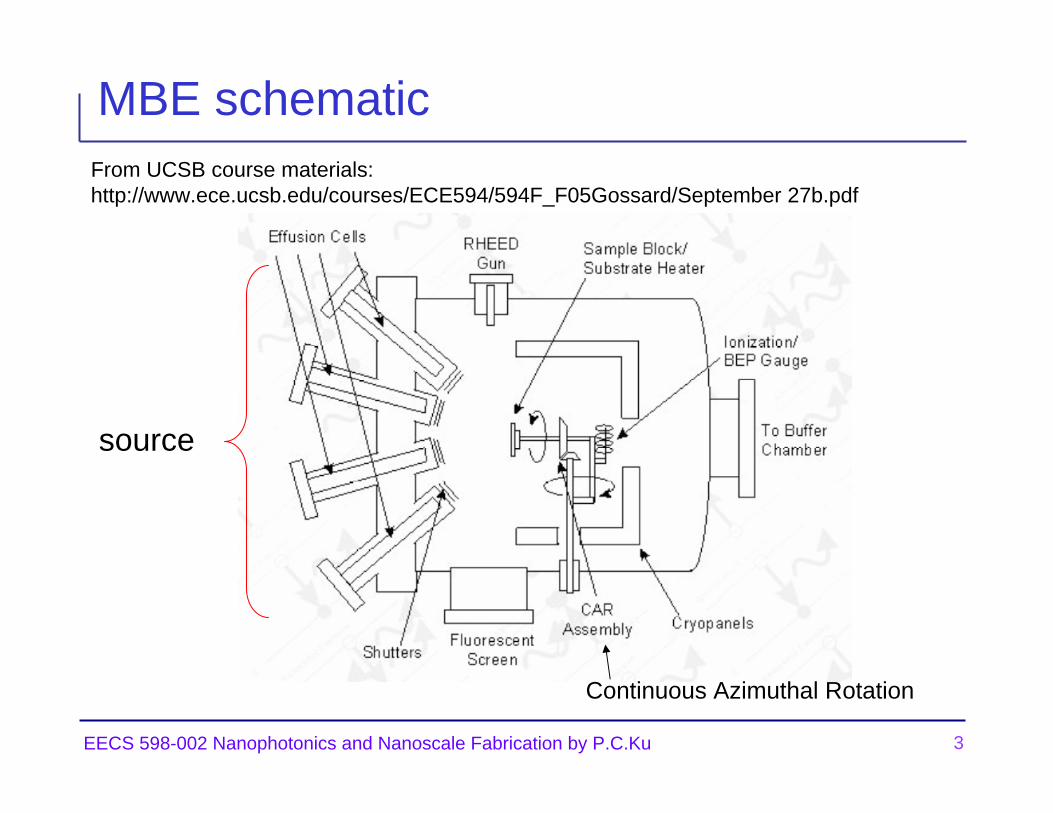
MBE schematic
source
Continuous Azimuthal Rotation
From UCSB course materials: http://www.ece.ucsb.edu/courses/ECE594/594F_F05Gossard/September 27b.pdf
4EECS 598-002 Nanophotonics and Nanoscale Fabrication by P.C.Ku
MBE operation
MBE operates under an ultra-high vacuum (< 10-10 torr) environment. That means during growth, the background residual gas such as H2O, CO2, and etc have negligible partial pressures compared to the sources.
The source either evaporates at ~ 600。C (solid-source MBE) or cracks into elemental form (gas-source MBE) and deposits onto a heated substrate (~ 400。C).
5EECS 598-002 Nanophotonics and Nanoscale Fabrication by P.C.Ku
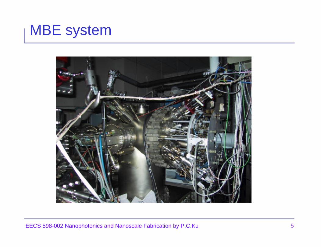
MBE system
6EECS 598-002 Nanophotonics and Nanoscale Fabrication by P.C.Ku
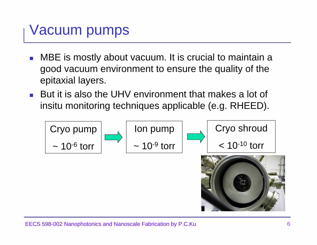
Vacuum pumps
MBE is mostly about vacuum. It is crucial to maintain a good vacuum environment to ensure the quality of the epitaxial layers.But it is also the UHV environment that makes a lot of insitu monitoring techniques applicable (e.g. RHEED).
Cryo pump
~ 10-6 torr
Ion pump
~ 10-9 torr
Cryo shroud
< 10-10 torr
7EECS 598-002 Nanophotonics and Nanoscale Fabrication by P.C.Ku
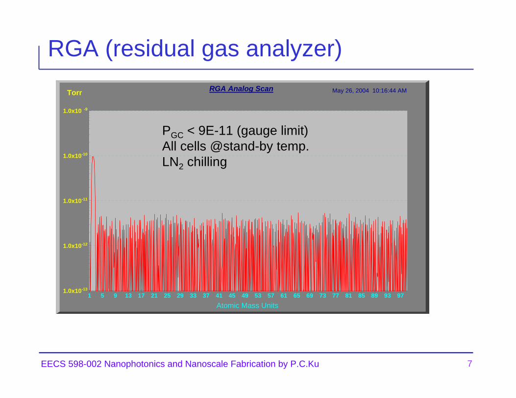
RGA (residual gas analyzer)
1 5 9 13 17 21 25 29 33 37 41 45 49 53 57 61 65 69 73 77 81 85 89 93 97-131.0x10
-121.0x10
-111.0x10
-101.0x10
-91.0x10
Atomic Mass Units
Torr RGA Analog Scan May 26, 2004 10:16:44 AM
PGC < 9E-11 (gauge limit)All cells @stand-by temp.LN2 chilling
8EECS 598-002 Nanophotonics and Nanoscale Fabrication by P.C.Ku
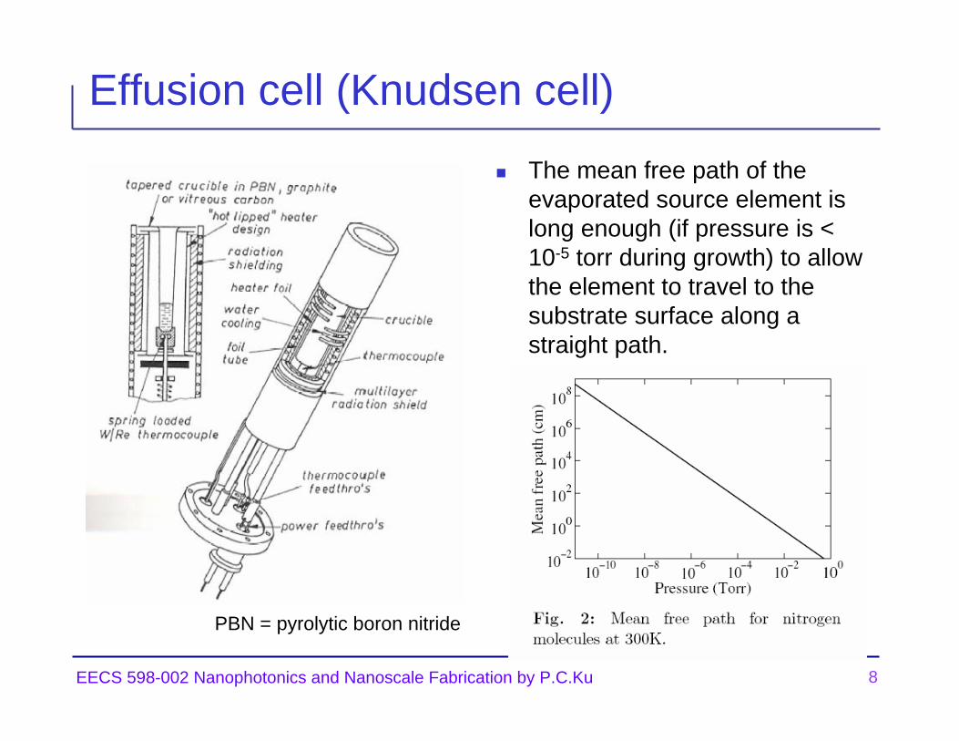
Effusion cell (Knudsen cell)
The mean free path of the evaporated source element is long enough (if pressure is < 10-5 torr during growth) to allow the element to travel to the substrate surface along a straight path.
PBN = pyrolytic boron nitride
9EECS 598-002 Nanophotonics and Nanoscale Fabrication by P.C.Ku
10EECS 598-002 Nanophotonics and Nanoscale Fabrication by P.C.Ku
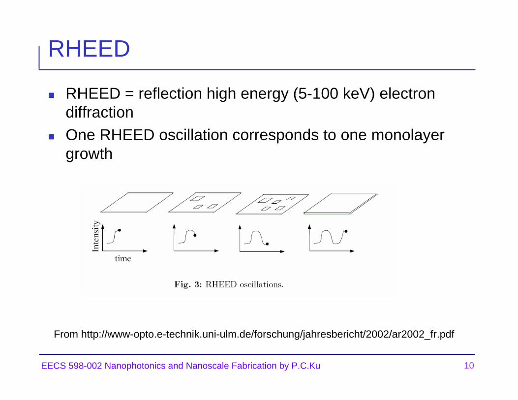
RHEED
RHEED = reflection high energy (5-100 keV) electron diffractionOne RHEED oscillation corresponds to one monolayer growth
From http://www-opto.e-technik.uni-ulm.de/forschung/jahresbericht/2002/ar2002_fr.pdf
11EECS 598-002 Nanophotonics and Nanoscale Fabrication by P.C.Ku
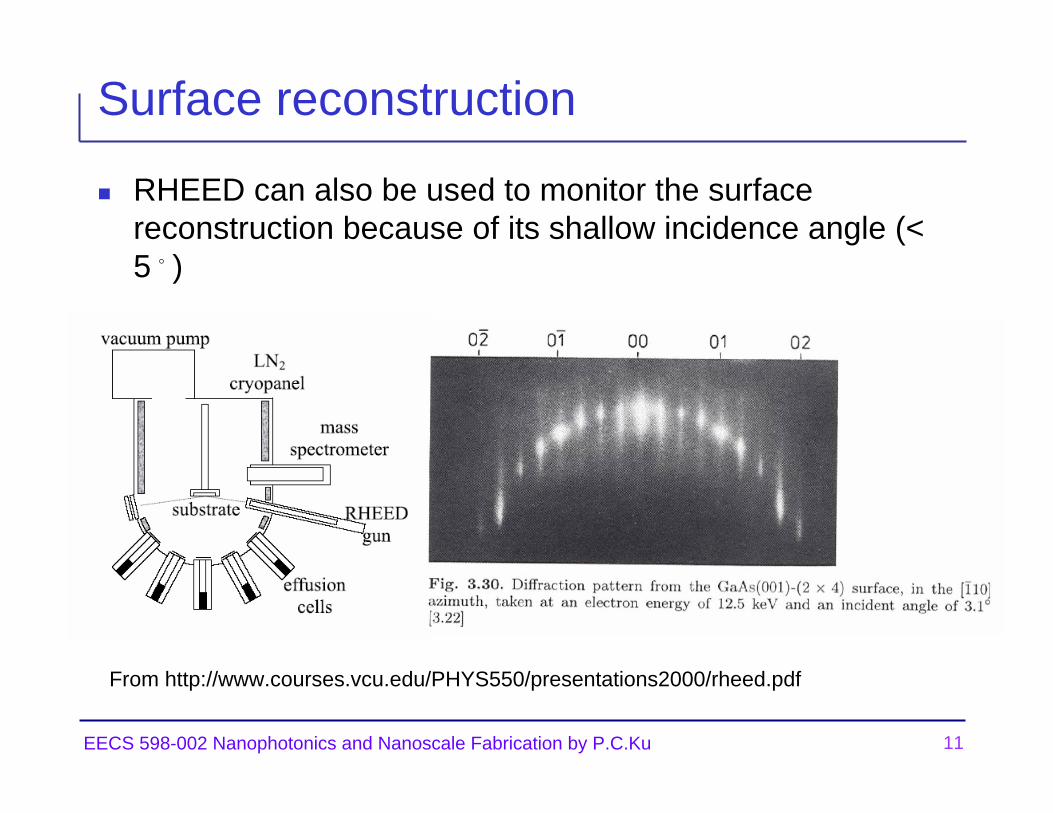
Surface reconstruction
RHEED can also be used to monitor the surface reconstruction because of its shallow incidence angle (< 5。)
From http://www.courses.vcu.edu/PHYS550/presentations2000/rheed.pdf
12EECS 598-002 Nanophotonics and Nanoscale Fabrication by P.C.Ku
Free MBE simulator
http://uberfast.ece.ucsb.edu/~mgrund/kmcinteractive/kmcinteractive.html
Runs only on Mac OS
13EECS 598-002 Nanophotonics and Nanoscale Fabrication by P.C.Ku
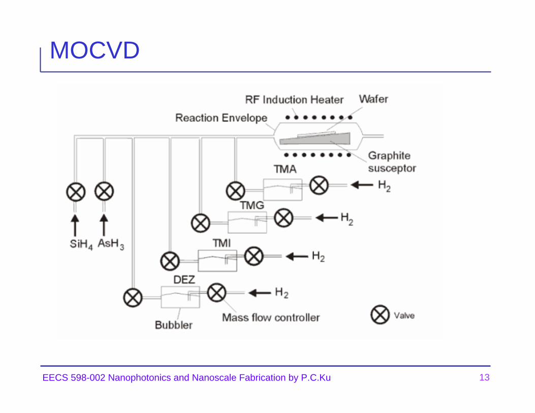
MOCVD
14EECS 598-002 Nanophotonics and Nanoscale Fabrication by P.C.Ku
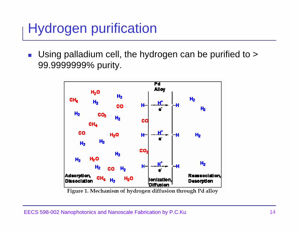
Hydrogen purification
Using palladium cell, the hydrogen can be purified to > 99.9999999% purity.
15EECS 598-002 Nanophotonics and Nanoscale Fabrication by P.C.Ku
MOCVD vs MBE
AdvantagesFaster growth rate (favored by industry)Wide temperature control range. Better film quality.Shorter system downtime
DisadvantagesToxic sources Huge set of parameters. Hard to control.Not UHV environment. Some insitu monitoring techniques are not applicable.
16EECS 598-002 Nanophotonics and Nanoscale Fabrication by P.C.Ku
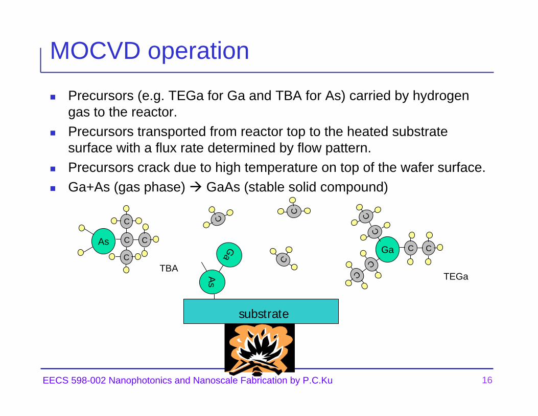
MOCVD operation
Precursors (e.g. TEGa for Ga and TBA for As) carried by hydrogen gas to the reactor.Precursors transported from reactor top to the heated substrate surface with a flux rate determined by flow pattern.Precursors crack due to high temperature on top of the wafer surface.Ga+As (gas phase) GaAs (stable solid compound)
As C
C
C
C
TBA
substrateAs
Ga C C
TEGa
CC
CC
Ga
C
CC
17EECS 598-002 Nanophotonics and Nanoscale Fabrication by P.C.Ku
18EECS 598-002 Nanophotonics and Nanoscale Fabrication by P.C.Ku
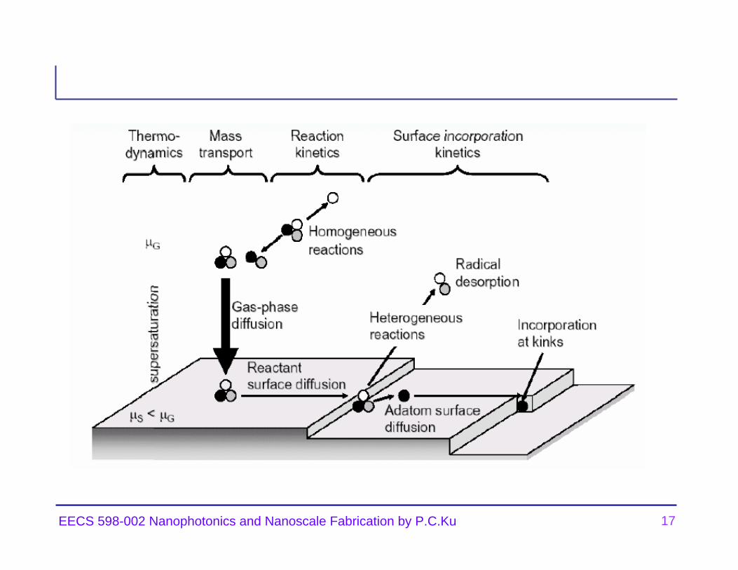
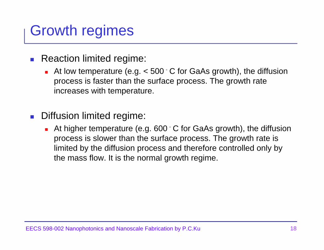
Growth regimes
Reaction limited regime:At low temperature (e.g. < 500。C for GaAs growth), the diffusion process is faster than the surface process. The growth rate increases with temperature.
Diffusion limited regime:At higher temperature (e.g. 600。C for GaAs growth), the diffusion process is slower than the surface process. The growth rate is limited by the diffusion process and therefore controlled only by the mass flow. It is the normal growth regime.
19EECS 598-002 Nanophotonics and Nanoscale Fabrication by P.C.Ku
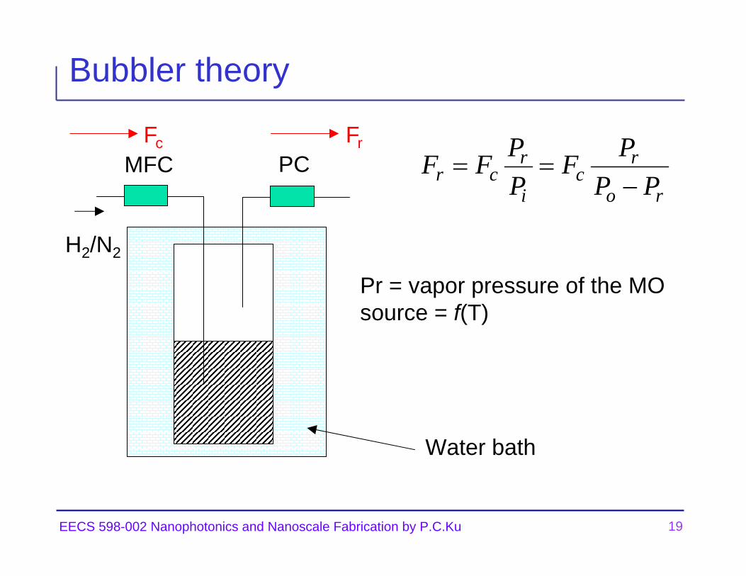
Bubbler theory
MFC
H2/N2
PCFc Fr
r rr c c
i o r
P PF F FP P P
= =−
Pr = vapor pressure of the MOsource = f(T)
Water bath
20EECS 598-002 Nanophotonics and Nanoscale Fabrication by P.C.Ku
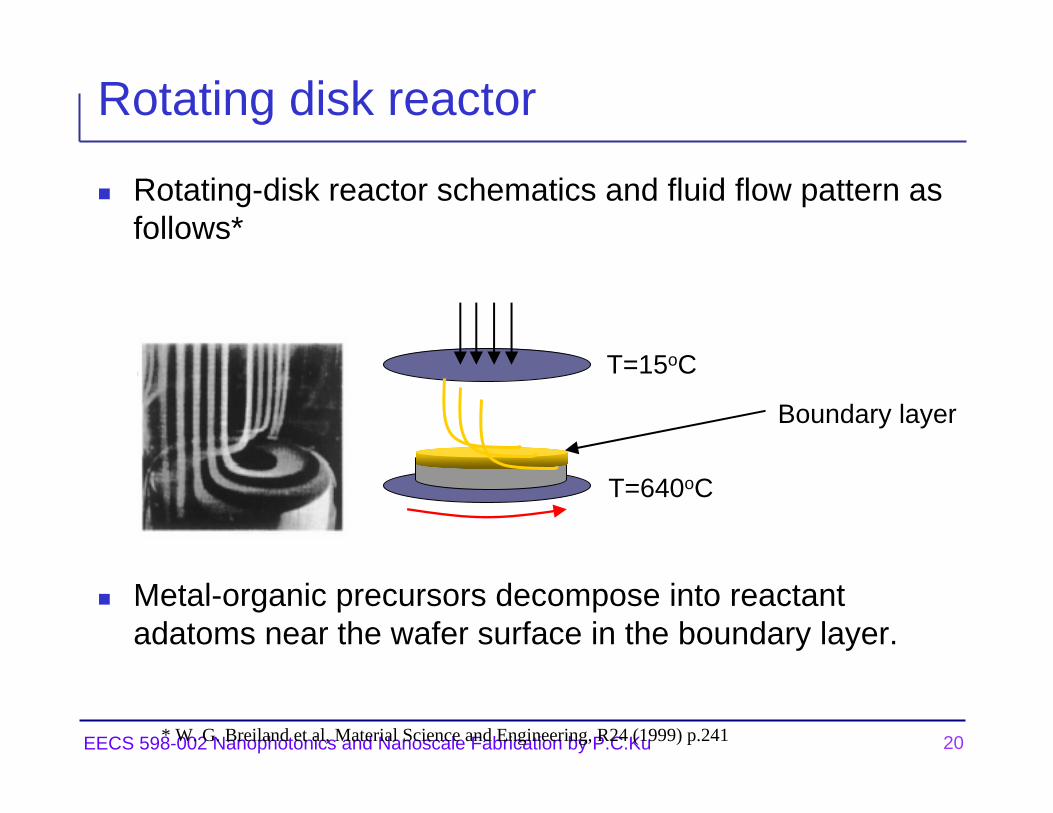
Rotating disk reactor
Rotating-disk reactor schematics and fluid flow pattern as follows*
Metal-organic precursors decompose into reactant adatoms near the wafer surface in the boundary layer.
* W. G. Breiland et al, Material Science and Engineering, R24 (1999) p.241
T=15oC
T=640oC
Boundary layer
21EECS 598-002 Nanophotonics and Nanoscale Fabrication by P.C.Ku
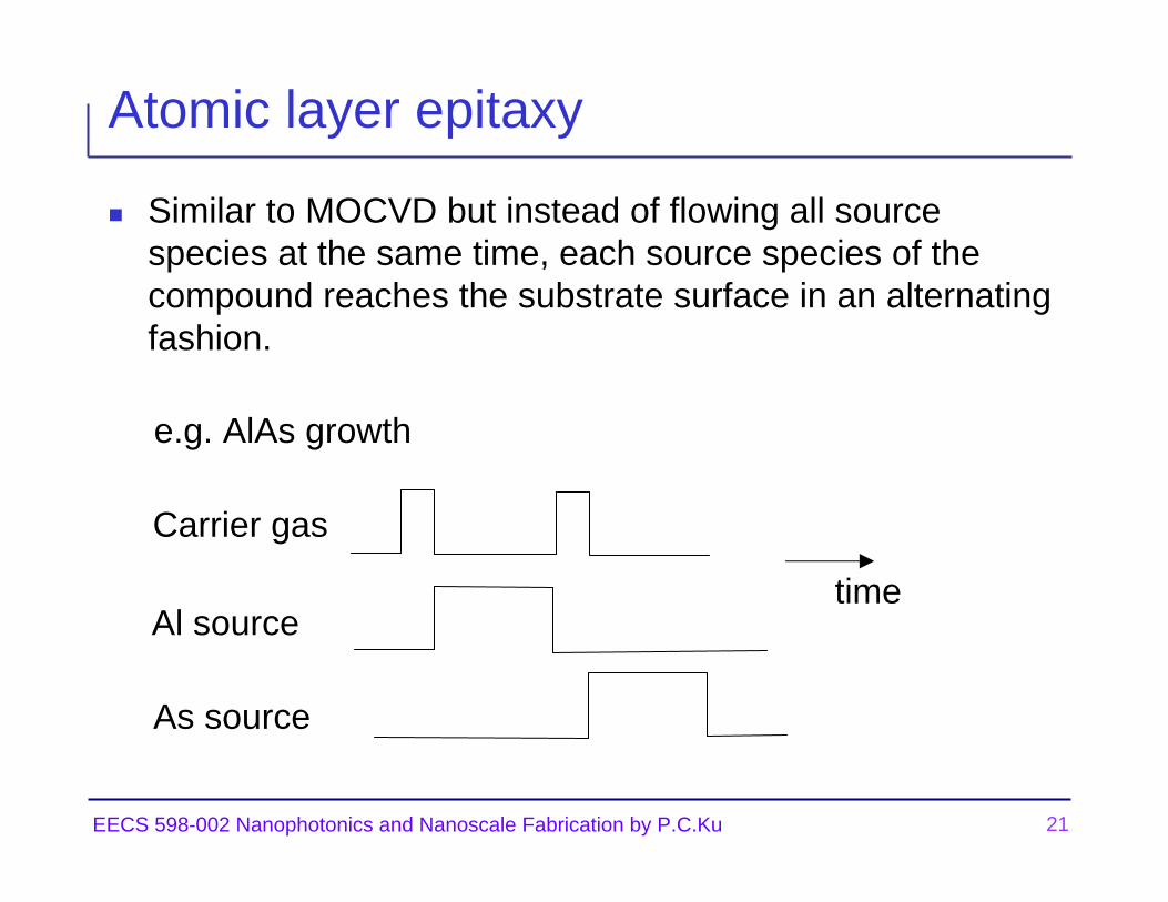
Atomic layer epitaxy
Similar to MOCVD but instead of flowing all source species at the same time, each source species of the compound reaches the substrate surface in an alternating fashion.
e.g. AlAs growth
Carrier gas
Al source
As source
time
22EECS 598-002 Nanophotonics and Nanoscale Fabrication by P.C.Ku
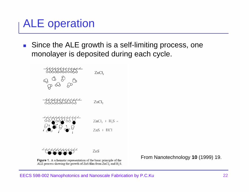
ALE operation
Since the ALE growth is a self-limiting process, one monolayer is deposited during each cycle.
From Nanotechnology 10 (1999) 19.