Embed Size (px)
DESCRIPTION
MOSFET LECTURE
Citation preview
Electronic DevicesKEEE 2224
Lecture 6Metal-Oxide-Semiconductor
Field Effect Transistor
Dr. Ghafour Amouzad Mahdiraji
October 2012
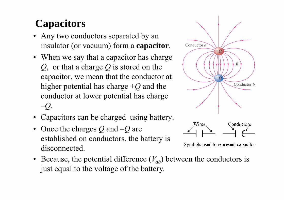
Capacitors• Any two conductors separated by an
insulator (or vacuum) form a capacitor.• When we say that a capacitor has charge Q, or that a charge Q is stored on the capacitor, we mean that the conductor at higher potential has charge +Q and the conductor at lower potential has charge –Q.
• Capacitors can be charged using battery.• Once the charges Q and –Q are
established on conductors, the battery is disconnected.
• Because, the potential difference (Vab) between the conductors is just equal to the voltage of the battery.
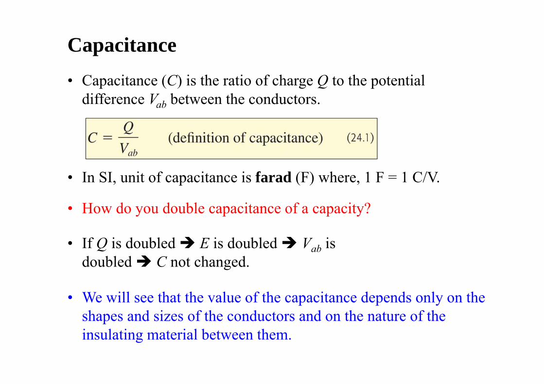
Capacitance
• If Q is doubled E is doubled Vab is doubled C not changed.
• We will see that the value of the capacitance depends only on the shapes and sizes of the conductors and on the nature of the insulating material between them.
• Capacitance (C) is the ratio of charge Q to the potential difference Vab between the conductors.
• In SI, unit of capacitance is farad (F) where, 1 F = 1 C/V.
• How do you double capacitance of a capacity?
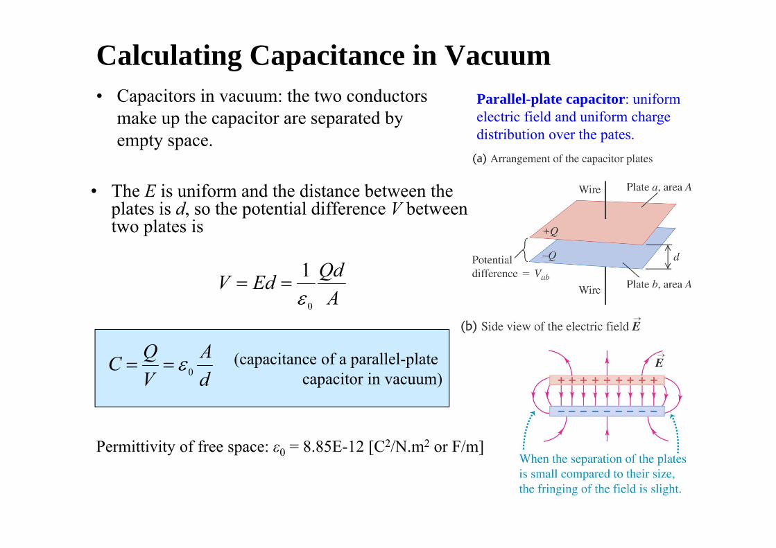
Calculating Capacitance in Vacuum
• The E is uniform and the distance between the plates is d, so the potential difference V between two plates is
• Capacitors in vacuum: the two conductors make up the capacitor are separated by empty space.
Parallel-plate capacitor: uniform electric field and uniform charge distribution over the pates.
Permittivity of free space: ε0 = 8.85E-12 [C2/N.m2 or F/m]
AQdEdV
0
1
(capacitance of a parallel-plate capacitor in vacuum)d
AVQC 0
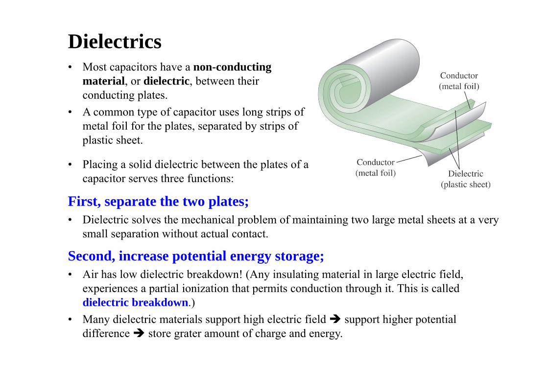
Dielectrics• Most capacitors have a non-conducting
material, or dielectric, between their conducting plates.
• A common type of capacitor uses long strips of metal foil for the plates, separated by strips of plastic sheet.
• Placing a solid dielectric between the plates of a capacitor serves three functions:
Second, increase potential energy storage;• Air has low dielectric breakdown! (Any insulating material in large electric field,
experiences a partial ionization that permits conduction through it. This is called dielectric breakdown.)
• Many dielectric materials support high electric field support higher potential difference store grater amount of charge and energy.
First, separate the two plates;• Dielectric solves the mechanical problem of maintaining two large metal sheets at a very
small separation without actual contact.
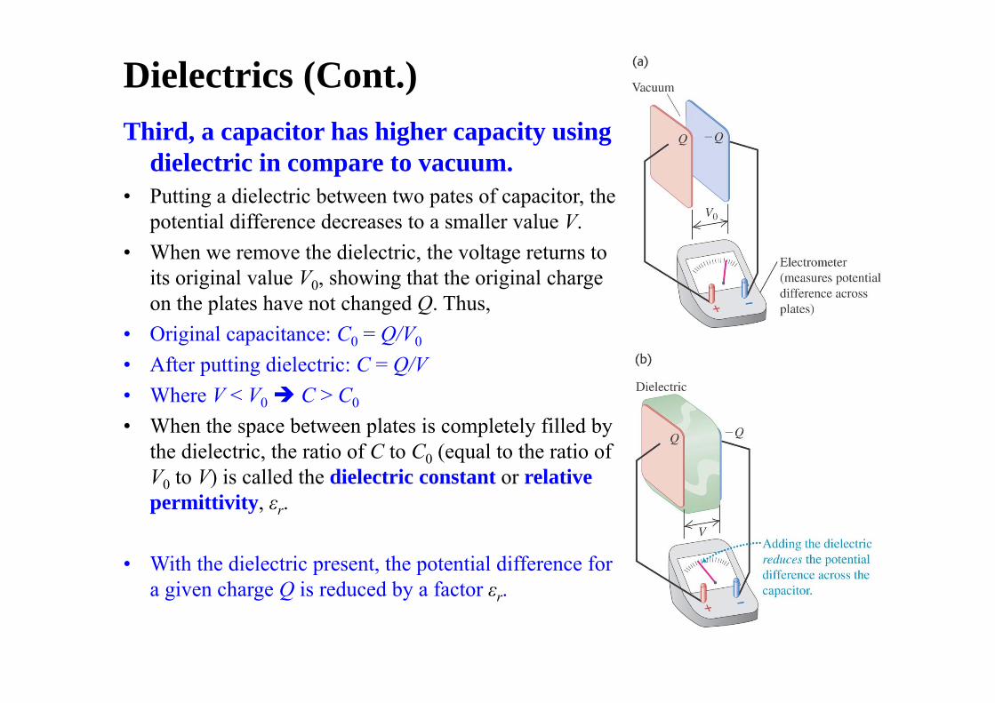
Dielectrics (Cont.)Third, a capacitor has higher capacity using
dielectric in compare to vacuum.• Putting a dielectric between two pates of capacitor, the
potential difference decreases to a smaller value V.• When we remove the dielectric, the voltage returns to
its original value V0, showing that the original charge on the plates have not changed Q. Thus,
• Original capacitance: C0 = Q/V0
• After putting dielectric: C = Q/V• Where V < V0 C > C0
• When the space between plates is completely filled by the dielectric, the ratio of C to C0 (equal to the ratio of V0 to V) is called the dielectric constant or relative permittivity, εr.
• With the dielectric present, the potential difference for a given charge Q is reduced by a factor εr.
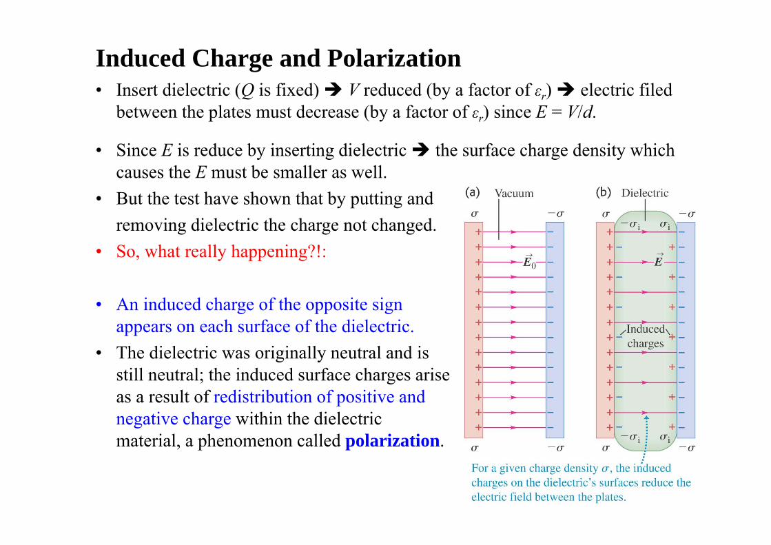
Induced Charge and Polarization• Insert dielectric (Q is fixed) V reduced (by a factor of εr) electric filed
between the plates must decrease (by a factor of εr) since E = V/d.
• Since E is reduce by inserting dielectric the surface charge density which causes the E must be smaller as well.
• But the test have shown that by putting and removing dielectric the charge not changed.
• So, what really happening?!:
• An induced charge of the opposite sign appears on each surface of the dielectric.
• The dielectric was originally neutral and is still neutral; the induced surface charges arise as a result of redistribution of positive and negative charge within the dielectric material, a phenomenon called polarization.
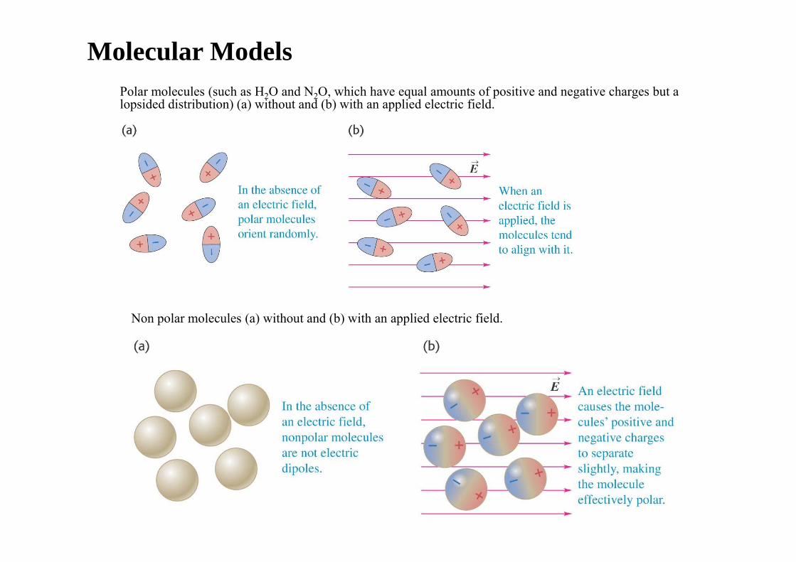
Molecular ModelsPolar molecules (such as H2O and N2O, which have equal amounts of positive and negative charges but a lopsided distribution) (a) without and (b) with an applied electric field.
Non polar molecules (a) without and (b) with an applied electric field.
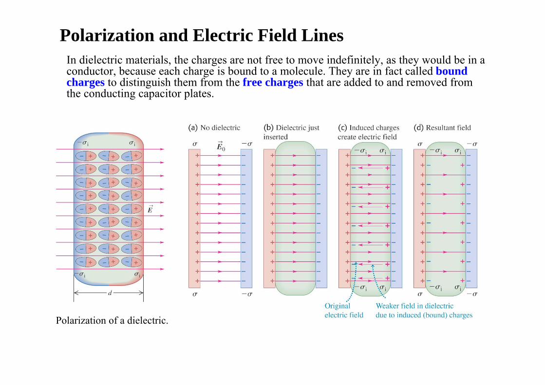
Polarization and Electric Field LinesIn dielectric materials, the charges are not free to move indefinitely, as they would be in a conductor, because each charge is bound to a molecule. They are in fact called boundcharges to distinguish them from the free charges that are added to and removed from the conducting capacitor plates.
Polarization of a dielectric.
The Two-Terminal MOS Structure
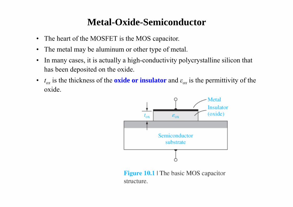
Metal-Oxide-Semiconductor• The heart of the MOSFET is the MOS capacitor.• The metal may be aluminum or other type of metal.• In many cases, it is actually a high-conductivity polycrystalline silicon that
has been deposited on the oxide.• tox is the thickness of the oxide or insulator and εox is the permittivity of the
oxide.
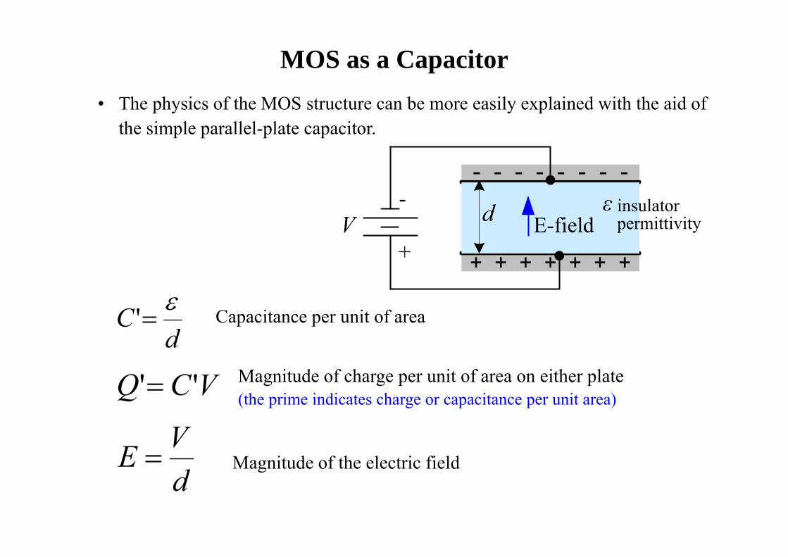
MOS as a Capacitor• The physics of the MOS structure can be more easily explained with the aid of
the simple parallel-plate capacitor.
d εV
dC '
VCQ ''
dVE
Capacitance per unit of area
Magnitude of charge per unit of area on either plate(the prime indicates charge or capacitance per unit area)
Magnitude of the electric field
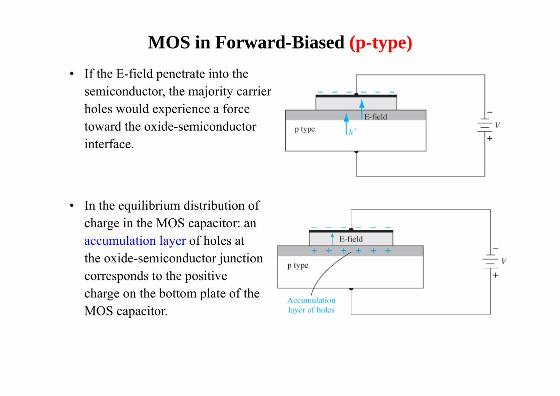
MOS in Forward-Biased (p-type)• If the E-field penetrate into the
semiconductor, the majority carrier holes would experience a force toward the oxide-semiconductor interface.
• In the equilibrium distribution of charge in the MOS capacitor: an accumulation layer of holes at the oxide-semiconductor junction corresponds to the positive charge on the bottom plate of the MOS capacitor.
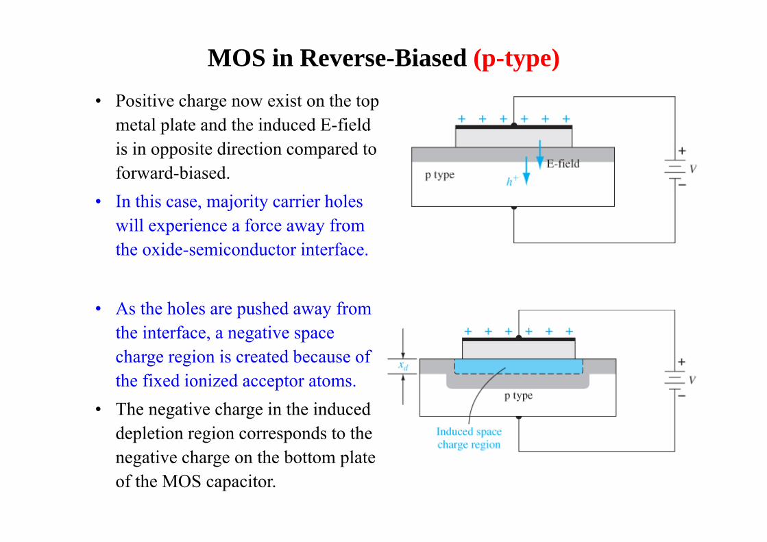
MOS in Reverse-Biased (p-type)• Positive charge now exist on the top
metal plate and the induced E-field is in opposite direction compared to forward-biased.
• In this case, majority carrier holes will experience a force away from the oxide-semiconductor interface.
• As the holes are pushed away from the interface, a negative space charge region is created because of the fixed ionized acceptor atoms.
• The negative charge in the induced depletion region corresponds to the negative charge on the bottom plate of the MOS capacitor.
MOS Energy-Band Diagrams (p-type)
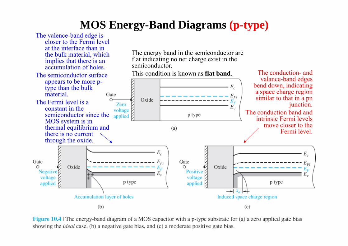
The energy band in the semiconductor are flat indicating no net charge exist in the semiconductor. This condition is known as flat band.
The valence-band edge is closer to the Fermi level at the interface than in the bulk material, which implies that there is an accumulation of holes.
The semiconductor surface appears to be more p-type than the bulk material.
The Fermi level is a constant in the semiconductor since the MOS system is in thermal equilibrium and there is no current through the oxide.
The conduction- and valance-band edges
bend down, indicating a space charge region similar to that in a pn
junction.The conduction band and
intrinsic Fermi levels move closer to the
Fermi level.
MOS Energy-Band Diagram (p-type)under Large Reverse-Biased
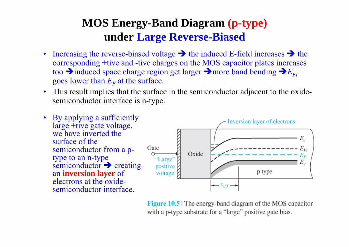
• By applying a sufficiently large +tive gate voltage, we have inverted the surface of the semiconductor from a p-type to an n-type semiconductor creating an inversion layer of electrons at the oxide-semiconductor interface.
• Increasing the reverse-biased voltage the induced E-field increases the corresponding +tive and -tive charges on the MOS capacitor plates increases too induced space charge region get larger more band bending EFigoes lower than EF at the surface.
• This result implies that the surface in the semiconductor adjacent to the oxide-semiconductor interface is n-type.
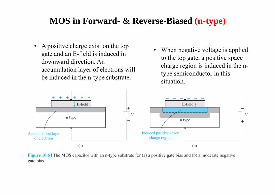
MOS in Forward- & Reverse-Biased (n-type)
• A positive charge exist on the top gate and an E-field is induced in downward direction. An accumulation layer of electrons will be induced in the n-type substrate.
• When negative voltage is applied to the top gate, a positive space charge region is induced in the n-type semiconductor in this situation.
MOS Energy-Band Diagrams (n-type)
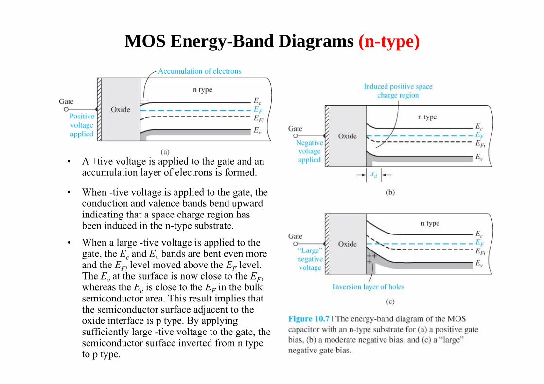
• When -tive voltage is applied to the gate, the conduction and valence bands bend upward indicating that a space charge region has been induced in the n-type substrate.
• When a large -tive voltage is applied to the gate, the Ec and Ev bands are bent even more and the EFi level moved above the EF level. The Ev at the surface is now close to the EF, whereas the Ec is close to the EF in the bulk semiconductor area. This result implies that the semiconductor surface adjacent to the oxide interface is p type. By applying sufficiently large -tive voltage to the gate, the semiconductor surface inverted from n type to p type.
• A +tive voltage is applied to the gate and an accumulation layer of electrons is formed.
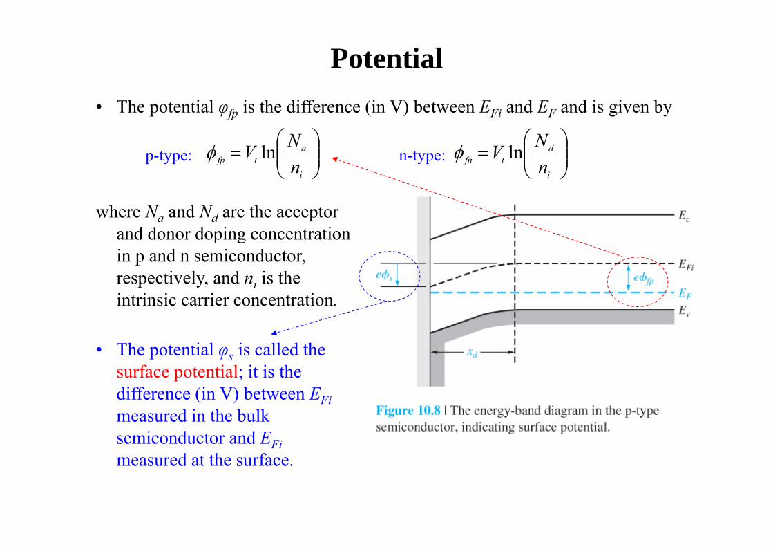
Potential • The potential φfp is the difference (in V) between EFi and EF and is given by
i
atfp n
NV ln
where Na and Nd are the acceptor and donor doping concentration in p and n semiconductor, respectively, and ni is the intrinsic carrier concentration.
i
dtfn n
NV lnp-type: n-type:
• The potential φs is called the surface potential; it is the difference (in V) between EFimeasured in the bulk semiconductor and EFimeasured at the surface.
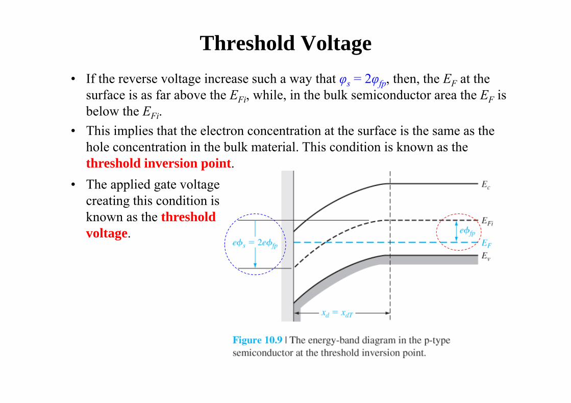
Threshold Voltage • If the reverse voltage increase such a way that φs = 2φfp, then, the EF at the
surface is as far above the EFi, while, in the bulk semiconductor area the EF is below the EFi.
• This implies that the electron concentration at the surface is the same as the hole concentration in the bulk material. This condition is known as the threshold inversion point.
• The applied gate voltage creating this condition is known as the threshold voltage.
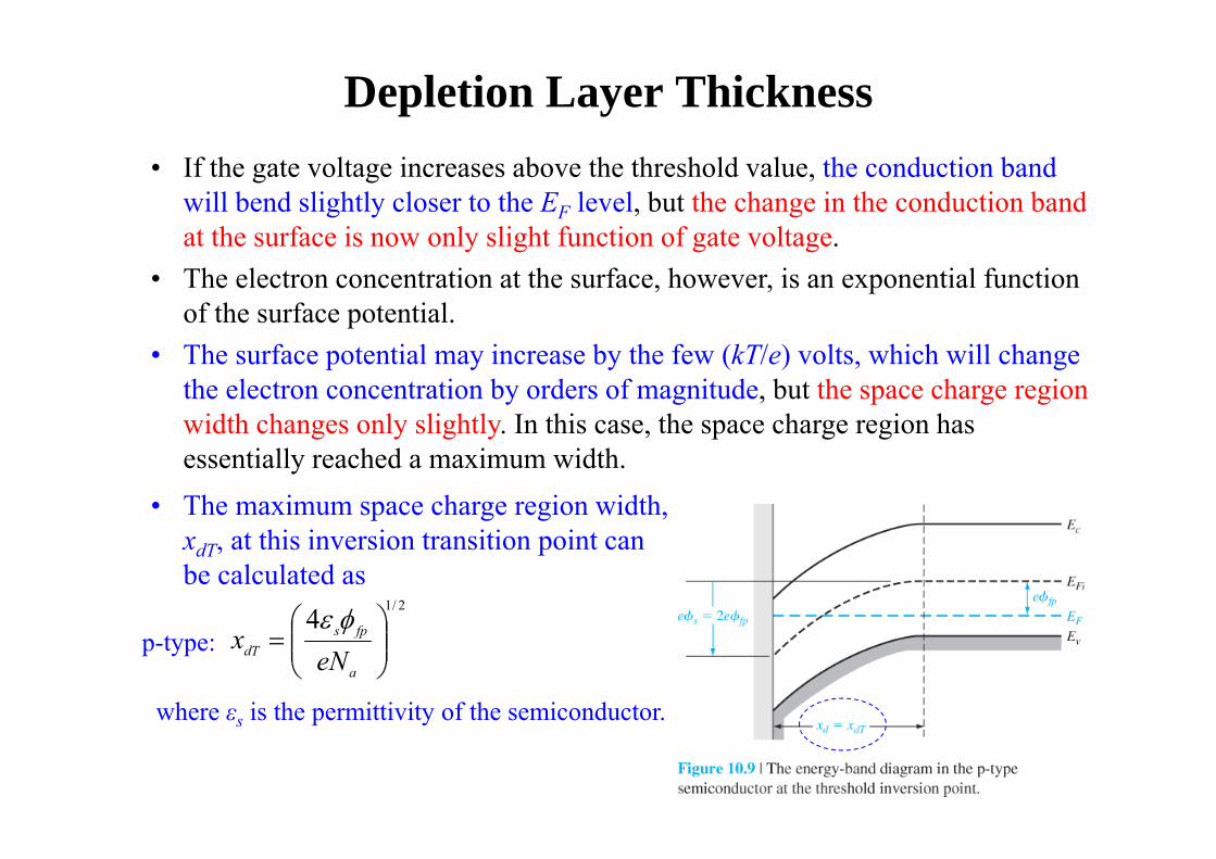
Depletion Layer Thickness • If the gate voltage increases above the threshold value, the conduction band
will bend slightly closer to the EF level, but the change in the conduction band at the surface is now only slight function of gate voltage.
• The electron concentration at the surface, however, is an exponential function of the surface potential.
• The surface potential may increase by the few (kT/e) volts, which will change the electron concentration by orders of magnitude, but the space charge region width changes only slightly. In this case, the space charge region has essentially reached a maximum width.
• The maximum space charge region width, xdT, at this inversion transition point can be calculated as
2/14
a
fpsdT eNx
p-type:
where εs is the permittivity of the semiconductor.
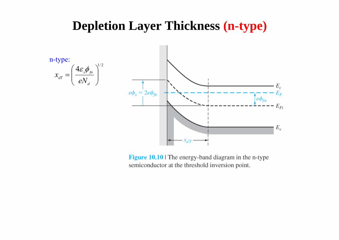
Depletion Layer Thickness (n-type)
2/14
d
fnsdT eNx
n-type:
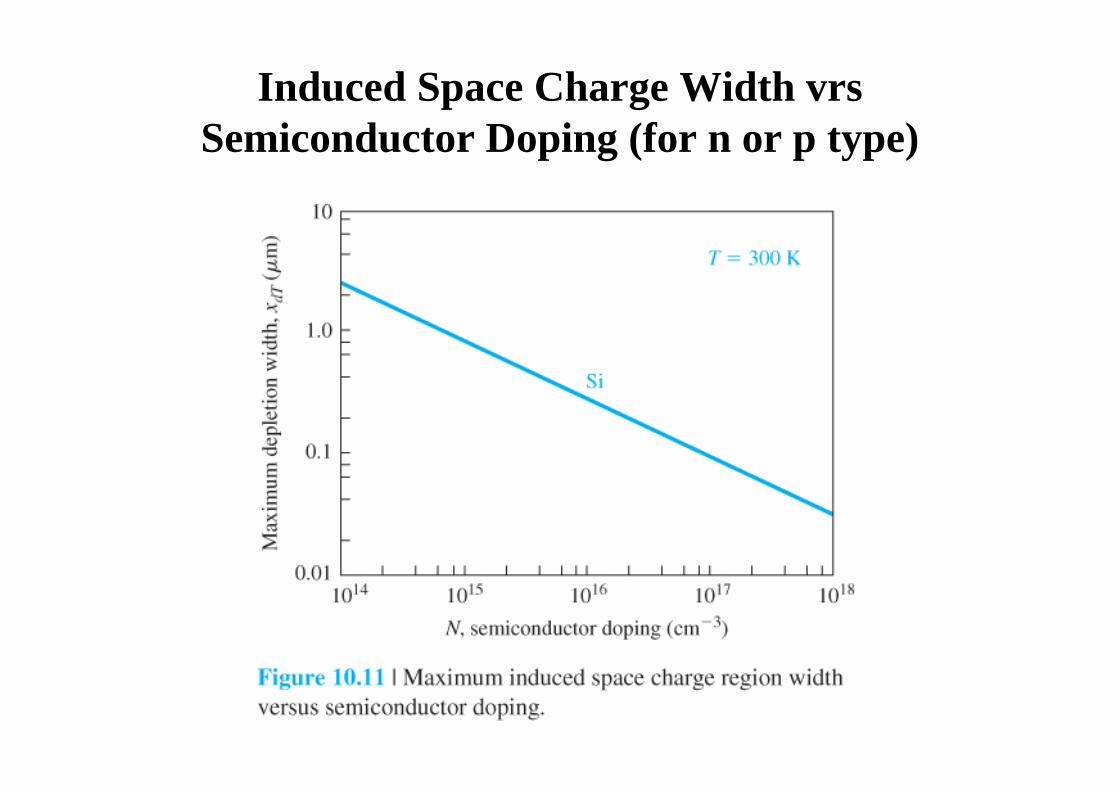
Induced Space Charge Width vrs Semiconductor Doping (for n or p type)
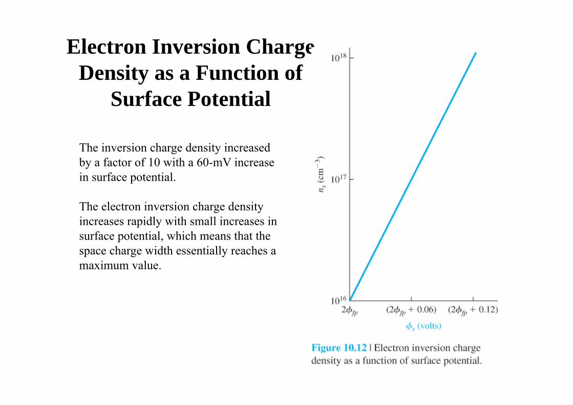
Electron Inversion Charge Density as a Function of
Surface Potential
The inversion charge density increased by a factor of 10 with a 60-mV increase in surface potential.
The electron inversion charge density increases rapidly with small increases in surface potential, which means that the space charge width essentially reaches a maximum value.
Example: • Calculate the maximum space charge width for a given semiconductor doping
concentration. Consider silicon at T = 300 K doped to Na = 1016 cm-3. The intrinsic carrier concentration is ni = 1.5 × 1010 cm-3.
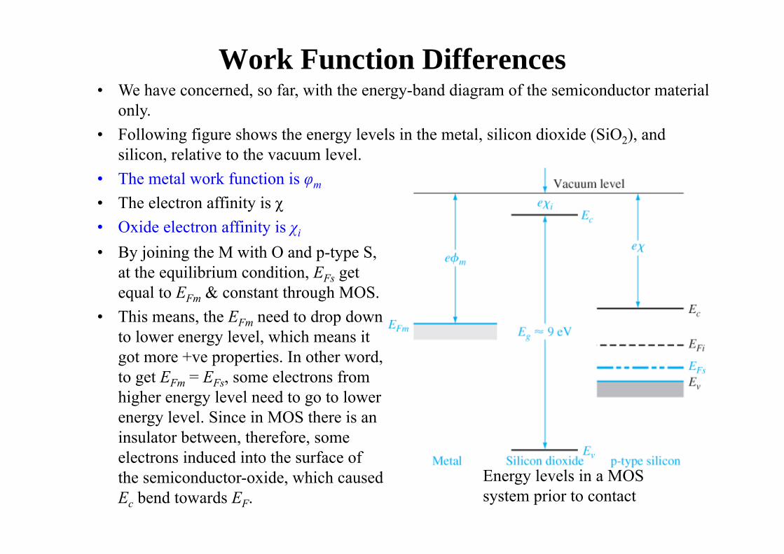
Work Function Differences• We have concerned, so far, with the energy-band diagram of the semiconductor material
only.• Following figure shows the energy levels in the metal, silicon dioxide (SiO2), and
silicon, relative to the vacuum level.• The metal work function is φm• The electron affinity is χ• Oxide electron affinity is χi
Energy levels in a MOS system prior to contact
• By joining the M with O and p-type S, at the equilibrium condition, EFs get equal to EFm & constant through MOS.
• This means, the EFm need to drop down to lower energy level, which means it got more +ve properties. In other word, to get EFm = EFs, some electrons from higher energy level need to go to lower energy level. Since in MOS there is an insulator between, therefore, some electrons induced into the surface of the semiconductor-oxide, which caused Ec bend towards EF.
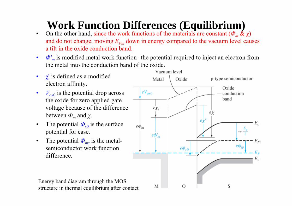
Work Function Differences (Equilibrium)• On the other hand, since the work functions of the materials are constant (Φm & χ)
and do not change, moving EFm down in energy compared to the vacuum level causes a tilt in the oxide conduction band.
• Φ'm is modified metal work function--the potential required to inject an electron from the metal into the conduction band of the oxide.
• χ' is defined as a modified electron affinity.
• Vox0 is the potential drop across the oxide for zero applied gate voltage because of the difference between Φm and χ.
• The potential Φs0 is the surface potential for case.
• The potential Φms is the metal-semiconductor work function difference.
Energy band diagram through the MOS structure in thermal equilibrium after contact
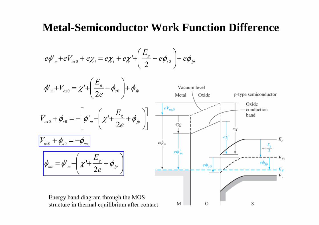
Metal-Semiconductor Work Function Difference
Energy band diagram through the MOS structure in thermal equilibrium after contact
fpsg
iioxm eeE
eeeeVe
00 2
''
fpsg
oxm eE
V
00 2
''
fp
gmsox e
EV
2''00
mssoxV 00
fp
gmms e
E
2''
Example• Determine the metal-semiconductor work function difference, Φms , for a given MOS
system and semiconductor doping.• For an aluminum-silicon dioxide junction, Φ’m = 3.2 V and, for a silicon-silicon
dioxide junction, χ' = 3.25 V. we may assume that Eg = 1.12 eV. Let the p-type doping be Na = 1015 cm-3.
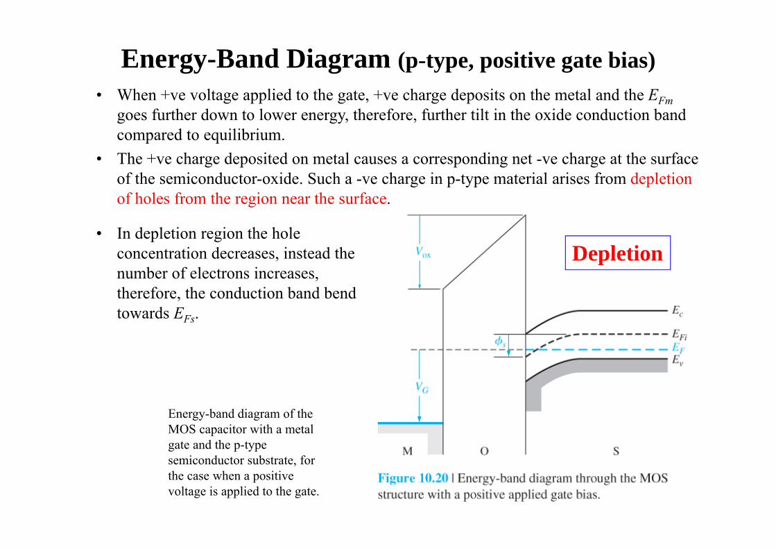
Energy-Band Diagram (p-type, positive gate bias)• When +ve voltage applied to the gate, +ve charge deposits on the metal and the EFm
goes further down to lower energy, therefore, further tilt in the oxide conduction band compared to equilibrium.
• The +ve charge deposited on metal causes a corresponding net -ve charge at the surface of the semiconductor-oxide. Such a -ve charge in p-type material arises from depletion of holes from the region near the surface.
Energy-band diagram of the MOS capacitor with a metal gate and the p-type semiconductor substrate, for the case when a positive voltage is applied to the gate.
• In depletion region the hole concentration decreases, instead the number of electrons increases, therefore, the conduction band bend towards EFs.
Depletion
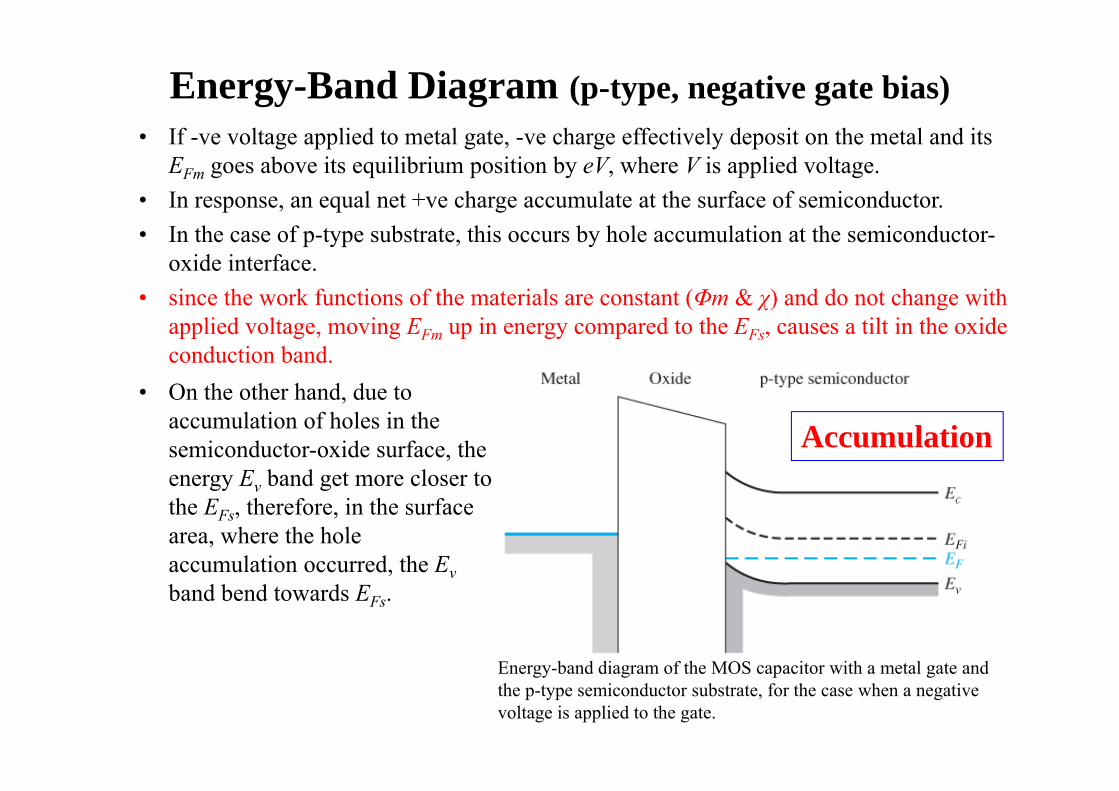
Energy-Band Diagram (p-type, negative gate bias)• If -ve voltage applied to metal gate, -ve charge effectively deposit on the metal and its EFm goes above its equilibrium position by eV, where V is applied voltage.
• In response, an equal net +ve charge accumulate at the surface of semiconductor.• In the case of p-type substrate, this occurs by hole accumulation at the semiconductor-
oxide interface.• since the work functions of the materials are constant (Φm & χ) and do not change with
applied voltage, moving EFm up in energy compared to the EFs, causes a tilt in the oxide conduction band.
Energy-band diagram of the MOS capacitor with a metal gate and the p-type semiconductor substrate, for the case when a negative voltage is applied to the gate.
Accumulation• On the other hand, due to
accumulation of holes in the semiconductor-oxide surface, the energy Ev band get more closer to the EFs, therefore, in the surface area, where the hole accumulation occurred, the Evband bend towards EFs.
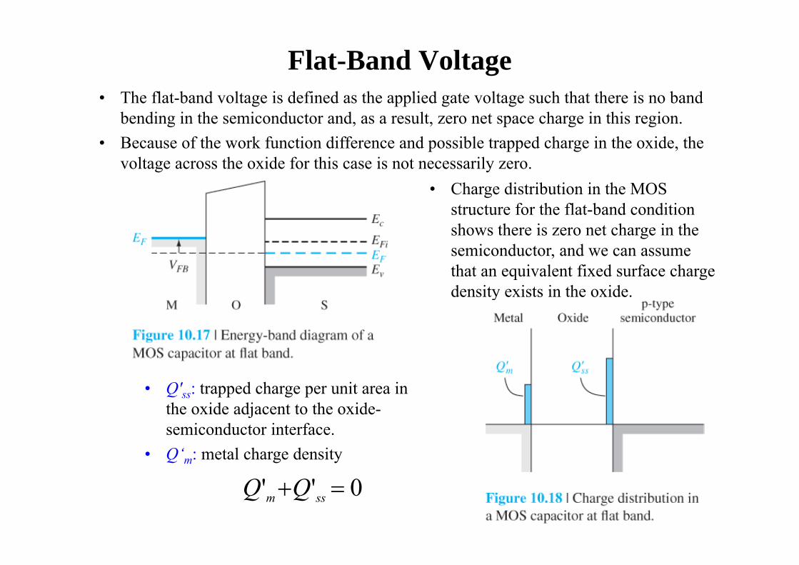
Flat-Band Voltage• The flat-band voltage is defined as the applied gate voltage such that there is no band
bending in the semiconductor and, as a result, zero net space charge in this region.• Because of the work function difference and possible trapped charge in the oxide, the
voltage across the oxide for this case is not necessarily zero.• Charge distribution in the MOS
structure for the flat-band condition shows there is zero net charge in the semiconductor, and we can assume that an equivalent fixed surface charge density exists in the oxide.
• Q'ss: trapped charge per unit area in the oxide adjacent to the oxide-semiconductor interface.
• Q‘m: metal charge density
0'' ssm QQ
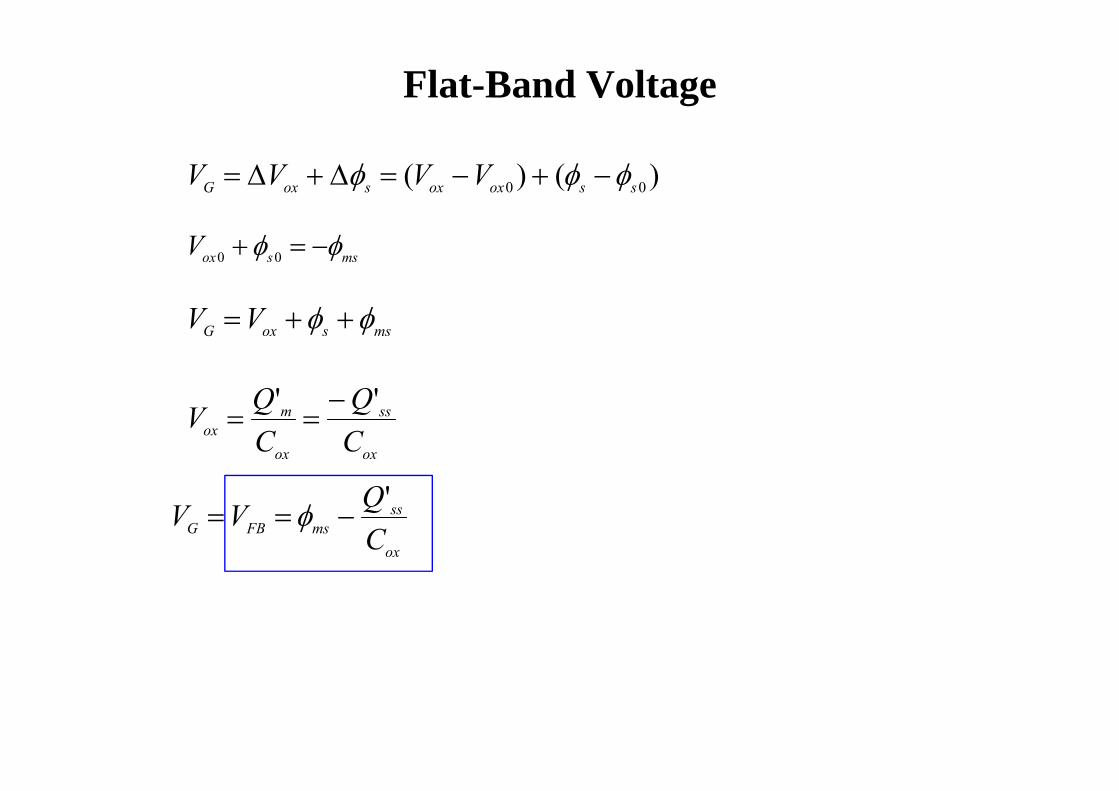
Flat-Band Voltage
)()( 00 ssoxoxsoxG VVVV
mssoxV 00
mssoxG VV
ox
ss
ox
mox C
QCQV ''
ox
ssmsFBG C
QVV '
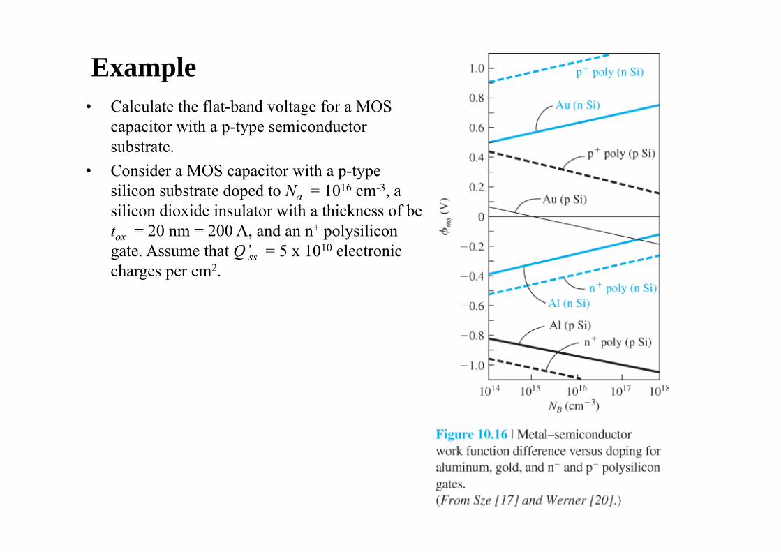
Example• Calculate the flat-band voltage for a MOS
capacitor with a p-type semiconductor substrate.
• Consider a MOS capacitor with a p-type silicon substrate doped to Na = 1016 cm-3, a silicon dioxide insulator with a thickness of be tox = 20 nm = 200 A, and an n+ polysilicon gate. Assume that Q’ss = 5 x 10¹⁰ electronic charges per cm2.
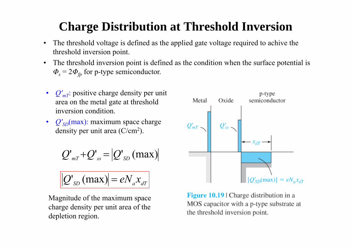
Charge Distribution at Threshold Inversion• The threshold voltage is defined as the applied gate voltage required to achive the
threshold inversion point.• The threshold inversion point is defined as the condition when the surface potential is Φs = 2Φfp for p-type semiconductor.
• Q'mT: positive charge density per unit area on the metal gate at threshold inversion condition.
• Q'SD(max): maximum space charge density per unit area (C/cm2).
(max)''' SDssmT QQQ
dTaSD xeNQ (max)'
Magnitude of the maximum space charge density per unit area of the depletion region.
Capacitance-Voltage Characteristics• A great deal of information about the MOS device and the oxide-semiconductor
interface can be obtained from the capacitance versus voltage or C-V characteristics of the device. The capacitance of a device is defined as
• The capacitance is a small-signal or ac parameter and is measured by superimposing a small ac voltage on an applied dc gate voltage.
• There are 3 operating conditions of interest in the MOS capacitor:• Accumulation• Depletion• Inversion
dVdQC
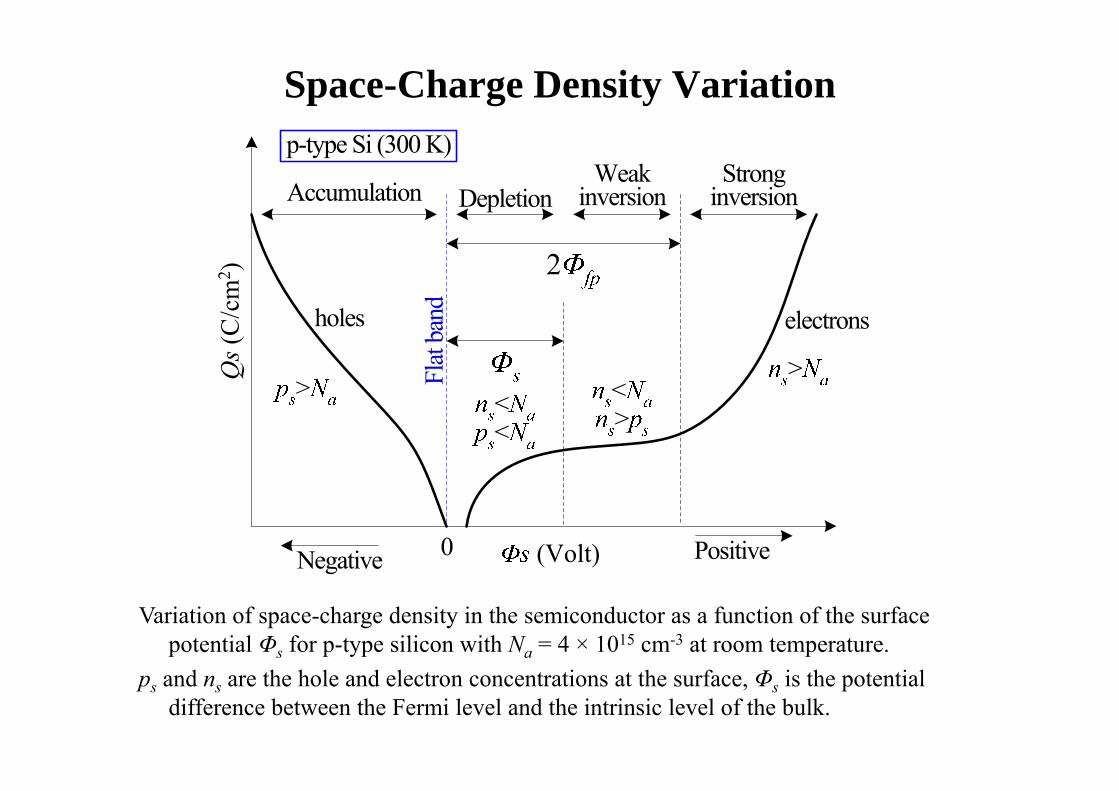
Space-Charge Density Variation
Variation of space-charge density in the semiconductor as a function of the surface potential Φs for p-type silicon with Na = 4 × 1015 cm-3 at room temperature.
ps and ns are the hole and electron concentrations at the surface, Φs is the potential difference between the Fermi level and the intrinsic level of the bulk.
Qs
2
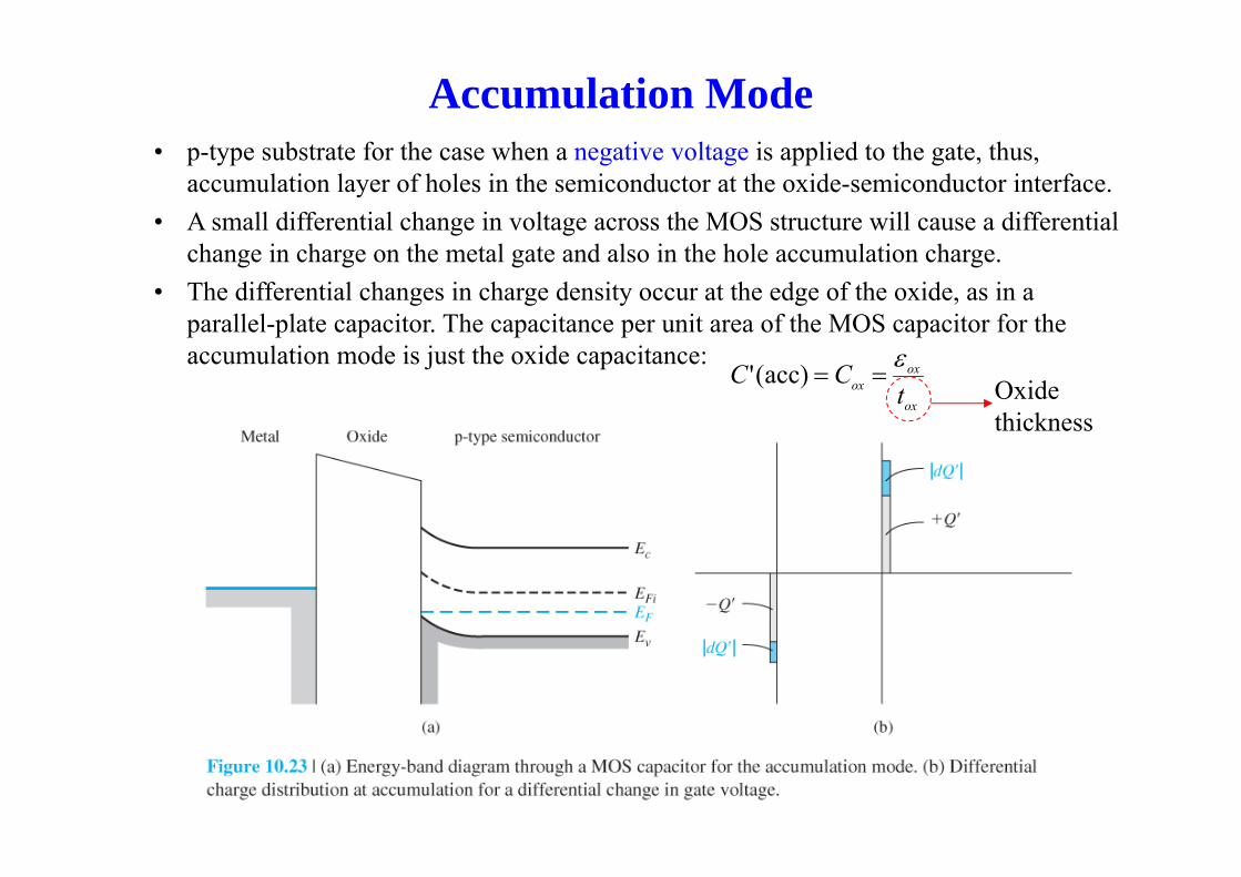
Accumulation Mode• p-type substrate for the case when a negative voltage is applied to the gate, thus,
accumulation layer of holes in the semiconductor at the oxide-semiconductor interface.• A small differential change in voltage across the MOS structure will cause a differential
change in charge on the metal gate and also in the hole accumulation charge.• The differential changes in charge density occur at the edge of the oxide, as in a
parallel-plate capacitor. The capacitance per unit area of the MOS capacitor for the accumulation mode is just the oxide capacitance:
ox
oxox tCC
)acc(' Oxide thickness
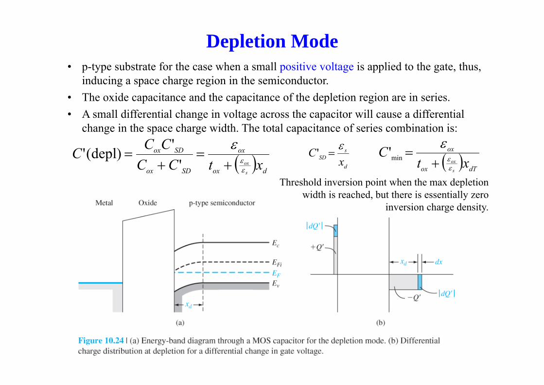
Depletion Mode• p-type substrate for the case when a small positive voltage is applied to the gate, thus,
inducing a space charge region in the semiconductor.• The oxide capacitance and the capacitance of the depletion region are in series.• A small differential change in voltage across the capacitor will cause a differential
change in the space charge width. The total capacitance of series combination is:
dox
ox
SDox
SDox
xtCCCCC
s
ox
'
')depl('d
sSD x
C ' dTox
ox
xtC
s
ox
min'
Threshold inversion point when the max depletion width is reached, but there is essentially zero
inversion charge density.
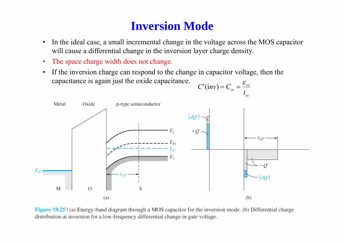
Inversion Mode• In the ideal case, a small incremental change in the voltage across the MOS capacitor
will cause a differential change in the inversion layer charge density.• The space charge width does not change.• If the inversion charge can respond to the change in capacitor voltage, then the
capacitance is again just the oxide capacitance.
ox
oxox tCnvC
)i('
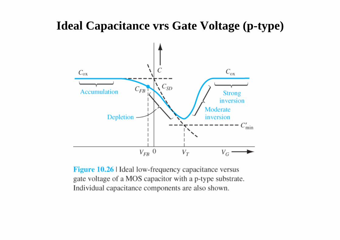
Ideal Capacitance vrs Gate Voltage (p-type)
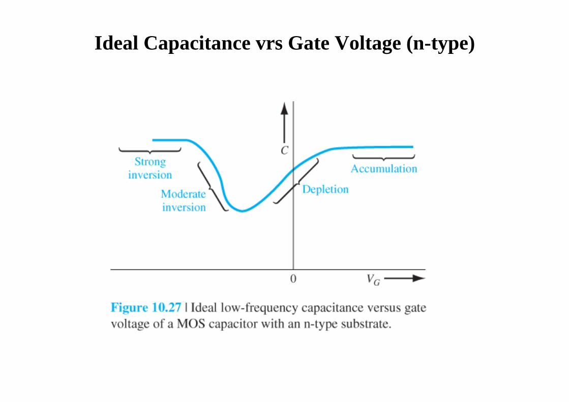
Ideal Capacitance vrs Gate Voltage (n-type)
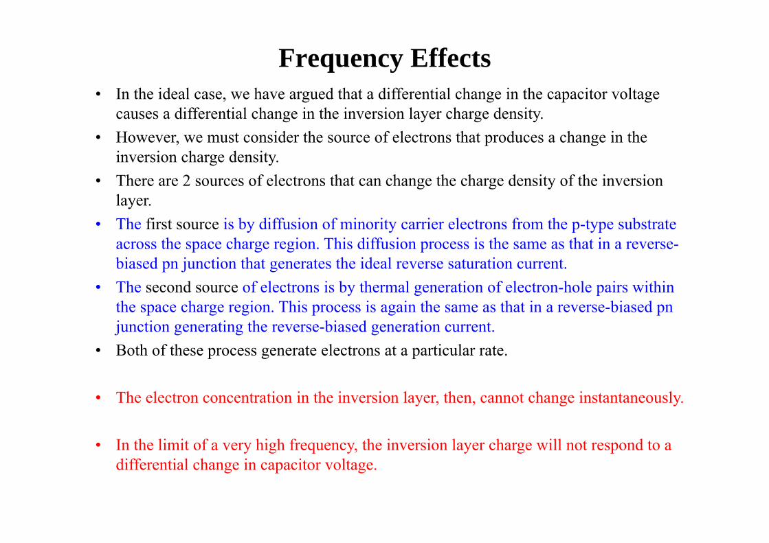
Frequency Effects• In the ideal case, we have argued that a differential change in the capacitor voltage
causes a differential change in the inversion layer charge density.• However, we must consider the source of electrons that produces a change in the
inversion charge density.• There are 2 sources of electrons that can change the charge density of the inversion
layer.• The first source is by diffusion of minority carrier electrons from the p-type substrate
across the space charge region. This diffusion process is the same as that in a reverse-biased pn junction that generates the ideal reverse saturation current.
• The second source of electrons is by thermal generation of electron-hole pairs within the space charge region. This process is again the same as that in a reverse-biased pn junction generating the reverse-biased generation current.
• Both of these process generate electrons at a particular rate.
• The electron concentration in the inversion layer, then, cannot change instantaneously.
• In the limit of a very high frequency, the inversion layer charge will not respond to a differential change in capacitor voltage.
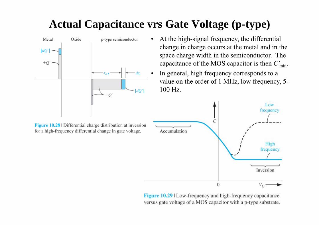
Actual Capacitance vrs Gate Voltage (p-type)• At the high-signal frequency, the differential
change in charge occurs at the metal and in the space charge width in the semiconductor. The capacitance of the MOS capacitor is then C'min.
• In general, high frequency corresponds to a value on the order of 1 MHz, low frequency, 5-100 Hz.


![The SOLUTIONS [MOS FET Relay] · [MOS FET Relay] When MOS FET relays are used under conditions that exceed the absolute maximum ratings even for a moment, it can be disruptive. To](https://img.pdfslide.net/doc/110x75/5f63b9a999108e331043de42/the-solutions-mos-fet-relay-mos-fet-relay-when-mos-fet-relays-are-used-under.jpg)


