Embed Size (px)
Citation preview

ECE 270 IM:PACT Introduction to Digital System Design © 2019 by D. G. Meyer
1
Lecture Summary – Module 4 Arithmetic and Computer Logic Circuits
Learning Outcome: an ability to analyze and design computer logic circuits Learning Objectives: 4-1. compare and contrast three different signed number notations: sign and magnitude, diminished
radix, and radix 4-2. convert a number from one signed notation to another 4-3. describe how to perform sign extension of a number represented using any of the three notation
schemes 4-4. perform radix addition and subtraction 4-5. describe the various conditions of interest following an arithmetic operation: overflow,
carry/borrow, negative, zero 4-6. describe the operation of a half-adder and write equations for its sum (S) and carry (C) outputs 4-7. describe the operation of a full adder and write equations for its sum (S) and carry (C) outputs 4-8. design a “population counting” or “vote counting” circuit using an array of half-adders and/or full-
adders 4-9. design an N-digit radix adder/subtractor circuit with condition codes 4-10. design a (signed or unsigned) magnitude comparator circuit that determines if A=B, A<B, or A>B 4-11. describe the operation of a carry look-ahead (CLA) adder circuit, and compare its performance to
that of a ripple adder circuit 4-12. define the CLA propagate (P) and generate (G) functions, and show how they can be realized using
a half-adder 4-13. write the equation for the carry out function of an arbitrary CLA bit position 4-14. draw a diagram depicting the overall organization of a CLA 4-15. determine the worst case propagation delay incurred by a practical (PLD-based) realization of a
CLA 4-16. describe how a “group ripple” adder can be constructed using N-bit CLA blocks 4-17. describe the operation of an unsigned multiplier array constructed using full adders 4-18. determine the full adder arrangement and organization (rows/diagonals) needed to construct an
NxM-bit unsigned multiplier array 4-19. determine the worst case propagation delay incurred by a practical (PLD-based) realization of an
NxM-bit unsigned multiplier array 4-20. describe the operation of a binary coded decimal (BCD) “correction circuit” 4-21. design a BCD full adder circuit 4-22. design a BCD N-digit radix (base 10) adder/subtractor circuit 4-23. define computer architecture, programming model, and instruction set 4-24. describe the top-down specification, bottom-up implementation strategy as it pertains to the design
of a computer 4-25. describe the characteristics of a “two address machine” 4-26. describe the contents of memory: program, operands, results of calculations 4-27. describe the format and fields of a basic machine instruction (opcode and address) 4-28. describe the purpose/function of each basic machine instruction (LDA, STA, ADD, SUB, AND,
HLT) 4-29. define what is meant by “assembly-level” instruction mnemonics 4-30. draw a diagram of a simple computer, showing the arrangement and interconnection of each
functional block

ECE 270 IM:PACT Introduction to Digital System Design © 2019 by D. G. Meyer
2
4-31. trace the execution of a computer program, identifying each step of an instruction’s microsequence
(fetch and execute cycles) 4-32. distinguish between synchronous and combinational system control signals 4-33. describe the operation of memory and the function of its control signals: MSL, MOE, and MWE 4-34. describe the operation of the program counter (PC) and the function of its control signals: ARS,
PCC, and POA 4-35. describe the operation of the instruction register (IR) and the function of its control signals: IRL and
IRA 4-36. describe the operation of the ALU and the function of its control signals: ALE, ALX, ALY, and
AOE 4-37. describe the operation of the instruction decoder/microsequencer and derive the system control table 4-38. describe the basic hardware-imposed system timing constraints: only one device can drive a bus
during a given machine cycle, and data cannot pass through more than one flip-flop (register) per cycle
4-39. discuss how the instruction register can be loaded with the contents of the memory location pointed to be the program counter and the program counter can be incremented on the same clock edge
4-40. modify a reference ALU design to perform different functions (e.g., shift and rotate) 4-41. describe how input/output instructions can be added to the base machine architecture 4-42. describe the operation of the I/O block and the function of its control signals: IOR and IOW 4-43. compare and contrast the operation of OUT instructions with and without a transparent latch as an
integral part of the I/O block 4-44. compare and contrast “jump” and “branch” transfer-of-control instructions along with the
architectural features needed to support them 4-45. distinguish conditional and unconditional branches 4-46. describe the basis for which a conditional branch is “taken” or “not taken” 4-47. describe the changes needed to the instruction decoder/microsequencer in order to dynamically
change the number of instruction execute cycles based on the opcode 4-48. compare and contrast the machine’s asynchronous reset (“START”) with the synchronous state
counter reset (“RST”) 4-49. describe the operation of a stack mechanism (LIFO queue) 4-50. describe the operation of the stack pointer (SP) register and the function of its control signals: ARS,
SPI, SPD, SPA 4-51. compare and contrast the two possible stack conventions: SP pointing to the top stack item vs. SP
pointing to the top stack item 4-52. describe how stack manipulation instructions (PSH/POP) can be added to the base machine
architecture 4-53. discuss the consequences of having an unbalanced set of PSH and POP instructions in a given
program 4-54. discuss the reasons for using a stack as a subroutine linkage mechanism: arbitrary nesting of
subroutine calls, passing parameters to subroutines, recursion, and reentrancy 4-55. describe how subroutine linkage instructions (JSR/RTS) can be added to the base machine
architecture 4-56. analyze the effect of changing the stack convention utilized (SP points to top stack item vs. next
available location) on instruction cycle counts

ECE 270 IM:PACT Introduction to Digital System Design © 2019 by D. G. Meyer
3
Lecture Summary – Module 4-A Signed Number Notation
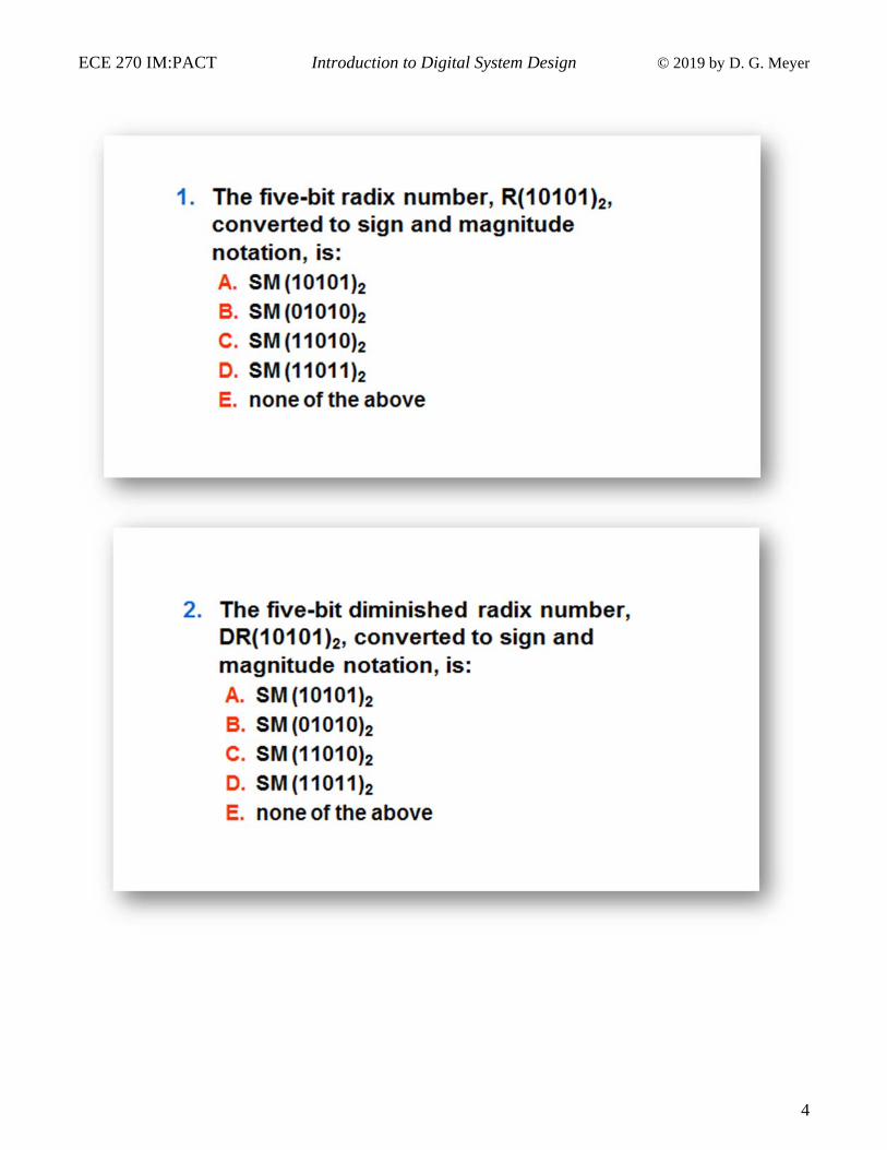
Reference: Digital Design Principles and Practices (4th Ed.) pp. 39-43, (5th Ed.) pp. 44-48 overview – signed number notations
o sign and magnitude (SM) o diminished radix (DR) o radix (R) o only negative numbers are different – positive numbers are the same in all 3 notations
sign and magnitude o vacuum tube vintage o left-most (“most significant”) digit is sign bit
0 positive R-1 negative (where R is radix or base of number)
o positive-negative pairs are called sign and magnitude complements of each other o negation method: replace sign digit (ns) with R-1-ns
diminished radix o most significant digit is still sign bit o positive-negative pairs are called diminished radix complements of each other o negation method: subtract each digit (including ns) from R-1, i.e. -(N)R = (Rn-1)R – (N)R
radix o most significant digit is still sign bit o positive-negative pairs are called radix complements of each other o negation method: add one to the DR complement of (N)R, i.e. -(N)R = (Rn)R – (N)R
comparison (3-bit signed numbers, each notation): simplifications for binary (base 2)
o SM: complement sign position (0 1) o DR (also called 1’s complement): complement each bit o R (also called 2’s complement):
add 1 to DR complement -or- scan number from right to left and complement each bit to the left of the first “1”
encountered
sign extension: SM – pad magnitude with leading zeroes; R and DR – replicate the sign digit
Observations: 1. SM and DR have a balanced set
of positive and negative numbers (as well as +0 and -0)
2. R notation has a single representation for zero, which results in an “extra negative number” – this unbalanced set of positive and negative numbers can lead to round-off errors in numeric computations
3. Virtually all computers in service today use R notation
ECE 270 IM:PACT Introduction to Digital System Design © 2019 by D. G. Meyer
4

ECE 270 IM:PACT Introduction to Digital System Design © 2019 by D. G. Meyer
5
Lecture Summary – Module 4-B Radix Addition and Subtraction
Reference: Digital Design Principles and Practices (4th Ed.) pp. 39-43, (5th Ed.) pp. 48-52
radix addition
o method: add all digits, including the sign digits; ignore any carry out of the sign position o note that overflow can occur, since we are working with numbers of fixed length
overflow occurs if two numbers of like sign are added and a result with the opposite sign is obtained
overflow cannot occur when adding numbers of opposite sign another way to detect overflow: if the carry in to the sign position is different than
the carry out of the sign position, then overflow has occurred when overflow occurs, there is no valid numeric result
radix subtraction o method: form the radix complement of the subtrahend and ADD (the same rules for
overflow detection apply)

ECE 270 IM:PACT Introduction to Digital System Design © 2019 by D. G. Meyer
6

ECE 270 IM:PACT Introduction to Digital System Design © 2019 by D. G. Meyer
7
Lecture Summary – Module 4-C Adder, Subtractor, and Comparator Circuits
Reference: DDPP (4th Ed.) pp. 458-466, 474-478; (5th Ed.) pp. 331-339, 341-345, 372-375 overview
o an adder circuit combines two operands based on rules described in 5-C o same addition rules apply for both signed (2’s complement) and unsigned numbers o subtraction performed by taking complement of subtrahend and performing add
building blocks
o half adder
Xi Yi Ci Si 0 0 0 1 1 0 1 1
o full adder
o “vote counting” application
Xi Yi Ci-1 Ci Si 0 0 0 0 0 1 0 1 0 0 1 1 1 0 0 1 0 1 1 1 0 1 1 1

ECE 270 IM:PACT Introduction to Digital System Design © 2019 by D. G. Meyer
8
ECE 270 IM:PACT Introduction to Digital System Design © 2019 by D. G. Meyer
9
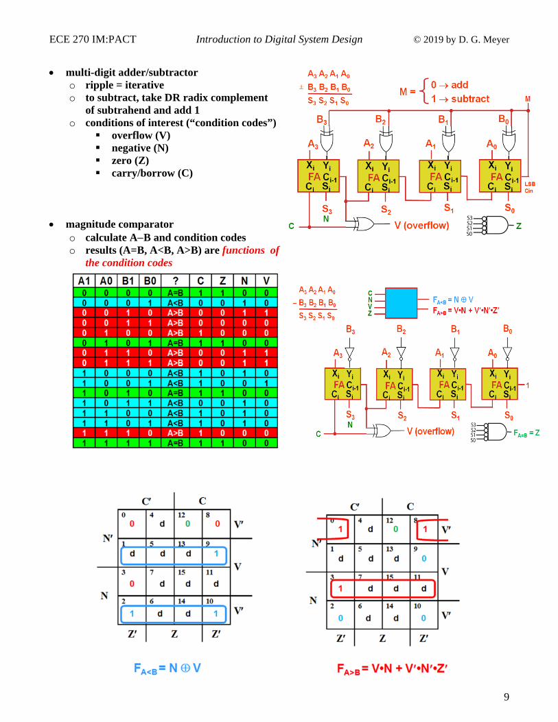
multi-digit adder/subtractor
o ripple = iterative o to subtract, take DR radix complement
of subtrahend and add 1 o conditions of interest (“condition codes”)
overflow (V) negative (N) zero (Z) carry/borrow (C)
magnitude comparator o calculate AB and condition codes o results (A=B, A<B, A>B) are functions of
the condition codes

ECE 270 IM:PACT Introduction to Digital System Design © 2019 by D. G. Meyer
10

ECE 270 IM:PACT Introduction to Digital System Design © 2019 by D. G. Meyer
11
Lecture Summary – Module 4-D Carry Look-Ahead (CLA) Adder Circuits
Reference: DDPP (4th Ed.) pp. 478-482, 484-488; (5th Ed.) pp. 376-383, 384-386 introduction
o previously considered iterative (“ripple”) adder circuit o problem: propagation delay increases with number of bits o solution: determine carries in parallel rather than iteratively significant speedup o “look-ahead” “anticipated”
definitions and derivations
o generate function (carry guaranteed) Gi = Xi•Yi o propagate function (carry in propagated out) Pi = Xi Yi o note that a “PG box” is just a half-adder (HA) o can rewrite sum bit equation as Si = Pi Ci-1 (C-1 is Cin) o can rewrite carry out equation as Ci = Gi + Ci-1•Pi
rewriting carry equations for 4-bit
adder in terms of P’s and G’s o C-1 = Cin
o C0 = G0 + Cin•P0
o C1 = G1 + C0•P1
o C2 = G2 + C1•P2
o C3 = Cout = G3 + C2•P3
rewriting carry equations for 4-
bit adder in terms of available inputs (successive expansion)
o C-1 = Cin
o C0 = G0 + Cin•P0
o C1 = G1 + C0•P1 = G1 + (G0 + Cin•P0)•P1 = G1 + G0 •P1 + Cin•P0•P1
o know what these equations are “saying”
o C2 = ______________________________________________________________________
o C3 = ______________________________________________________________________
observations
o regardless of adder length (number of operand bits), the time required to produce any sum digit is the same (i.e. they are all produced in parallel)
o large CLA adders are difficult to build in practice because of “product term explosion” o reasonable compromise is to make a group ripple adder (cascading m-bit CLA blocks
together to get desired operand length)

ECE 270 IM:PACT Introduction to Digital System Design © 2019 by D. G. Meyer
12
4-bit CLA realized in Verilog
alternate version using “+” (addition) operator
identical timing analysis for both versions “+” operator synthesizes CLA equations
module cla4(X, Y, CIN, S); input wire [3:0] X, Y; // Operands input wire CIN; // Carry in output wire [3:0] S; // Sum outputs wire [3:0] C; // Carry equations (C[3] is Cout) wire [3:0] P, G; assign G = X & Y; // Generate functions G[0] = X[0]&Y[0];
G[1] = .. so on assign P = X ^ Y; // Propagate functions P[0] = X[0]^Y[0];
P[1] = .. so on // Carry function definitions assign C[0] = G[0] | CIN & P[0]; assign C[1] = G[1] | G[0] & P[1] | CIN & P[0] & P[1]; assign C[2] = G[2] | G[1] & P[2] | G[0] & P[1] & P[2] | CIN & P[0] & P[1] & P[2]; assign C[3] = G[3] | G[2] & P[3] | G[1] & P[2] & P[3] | G[0] & P[1] & P[2] & P[3] | CIN & P[0] & P[1] & P[2] & P[3]; assign S[0] = CIN ^ P[0]; assign S[3:1] = C[2:0] ^ P[3:1]; endmodule
module cla4p(X, Y, CIN, S); input wire [3:0] X, Y; // Operands input wire CIN; // Carry in output wire [3:0] S; // Sum outputs assign S = X + Y + {3'b000,CIN}; endmodule
Timing Analysis for ispMACH 4256ZE 5.8 ns CPLD Delay Level Source Destination ===== ===== ====== =========== 6.40 1 CIN S3 6.40 1 X0 S3 6.40 1 Y0 S3 6.35 1 X1 S3 6.35 1 Y1 S3 6.30 1 X2 S3 6.30 1 Y2 S3 6.25 1 Y3 S3

ECE 270 IM:PACT Introduction to Digital System Design © 2019 by D. G. Meyer
13
Lecture Summary – Module 4-E Multiplier Circuits
Reference: DDPP (4th Ed.) pp. 45-47, 494-497; (5th Ed.) pp. 54-56, 416-419 overview
o consider 3x3 unsigned binary multiplication:
o based on “shift and add” algorithm o each row is called a product component o each xi•yj term represents a product component bit (logical AND) o the product P is obtained by adding together the product components
generalizations for an NxM multiplier array circuit
o N = number of bits in multiplicand o M = number of bits in multiplier o produces an N+M digit result o requires NxM AND gates to generate the product components o requires N-1 “diagonals” of full adders o requires M rows of full adders
exercise: 4x2 multiplier array circuit

ECE 270 IM:PACT Introduction to Digital System Design © 2019 by D. G. Meyer
14
exercise: 2x4 multiplier array circuit generalizations for an NxM multiplier
o N = number of bits in multiplicand (top) o M = number of bits in multiplier (bottom) o produces an N+M digit result o requires NxM AND gates to generate the product components o requires N–1 diagonals of full adders o requires M rows of full adders

ECE 270 IM:PACT Introduction to Digital System Design © 2019 by D. G. Meyer
15

ECE 270 IM:PACT Introduction to Digital System Design © 2019 by D. G. Meyer
16
realizations in Verilog
o use expressions to define product components o use addition operator (+) to form unsigned sum of product components o example: 4x4 multiplier array circuit
/* 4x4 Combinational Multiplier */module mul4x4(X, Y, P); input wire [3:0] X, Y; // Multiplicand, multiplier output wire [7:0] P; // Product bits wire [7:0] PC[3:0]; // Four 8-bit variables assign PC[0] = {8{Y[0]}} & {4'b0, X}; // 0000X3X2X1X0 assign PC[1] = {8{Y[1]}} & {3'b0, X, 1'b0}; // 000X3X2X1X00 assign PC[2] = {8{Y[2]}} & {2'b0, X, 2'b0}; // 00X3X2X1X000 assign PC[3] = {8{Y[3]}} & {1'b0, X, 3'b0}; // 0X3X2X1X0000 assign P = PC[0] + PC[1] + PC[2] + PC[3]; endmodule
Timing Analysis for ispMACH 4256ZE 5.8 ns CPLD Delay Level Source Destination ===== ===== ====== =========== 6.50 1 X0 P4 6.50 1 X0 P5 6.50 1 X1 P4 6.50 1 X1 P5 6.50 1 X2 P4 6.50 1 X2 P5 6.50 1 Y0 P4 6.50 1 Y0 P5 6.50 1 Y1 P4 6.50 1 Y1 P5 6.50 1 Y2 P4 6.50 1 Y2 P5 6.45 1 X3 P4 6.45 1 X3 P5 6.45 1 Y3 P4 6.45 1 Y3 P5 6.05 1 X0 P0 6.05 1 X0 P1 6.05 1 X0 P2 6.05 1 X0 P3

ECE 270 IM:PACT Introduction to Digital System Design © 2019 by D. G. Meyer
17
N10 Z4 Z3 Z2 Z1 Z0 Cout S3 S2 S1 S0 Correction0 0 0 0 0 0 0 0 0 0 0 <none>1 0 0 0 0 1 0 0 0 0 1 <none> 2 0 0 0 1 0 0 0 0 1 0 <none> 3 0 0 0 1 1 0 0 0 1 1 <none>4 0 0 1 0 0 0 0 1 0 0 <none>5 0 0 1 0 1 0 0 1 0 1 <none> 6 0 0 1 1 0 0 0 1 1 0 <none>7 0 0 1 1 1 0 0 1 1 1 <none>8 0 1 0 0 0 0 1 0 0 0 <none> 9 0 1 0 0 1 0 1 0 0 1 <none>10 0 1 0 1 0 1 0 0 0 0 <add 6> 11 0 1 0 1 1 1 0 0 0 1 <add 6>12 0 1 1 0 0 1 0 0 1 0 <add 6>13 0 1 1 0 1 1 0 0 1 1 <add 6> 14 0 1 1 1 0 1 0 1 0 0 <add 6>15 0 1 1 1 1 1 0 1 0 1 <add 6> 16 1 0 0 0 0 1 0 1 1 0 <add 6>17 1 0 0 0 1 1 0 1 1 1 <add 6>18 1 0 0 1 0 1 1 0 0 0 <add 6> 19 1 0 0 1 1 1 1 0 0 1 <add 6>
Lecture Summary – Module 4-F BCD Adder Circuits
Reference: Digital Design Principles and Practices (4th Ed.) pp. 48-51; (5th Ed.) pp. 58-60 overview
o external computer interfaces may need to read or display decimal digits (examples) o need to perform arithmetic operations on decimal numbers directly o most commonly used code in binary-coded decimal (BCD) o object is to design circuit that adds two BCD digit codes plus carry in, to produce a sum
digit plus a carry out o want to use standard 4-bit binary adder modules as “building blocks” o note that there are six “unused combinations” in BCD, so potential exists for needed to
perform a “correction” general circuit model examples of decimal addition and correction summary of rules
o if the sum of two BCD digits is 9 (i.e. 1001), no correction is needed
o if the sum of two BCD digits is > 9, the result must be corrected by adding six (0110)
“correction function” derivation
X3 X2 X1 X0 Y3 Y2 Y1 Y0
CinCout
S3 S2 S1 S0
4-bit Adder
Correction Circuit
Z4 Z3 Z2 Z1 Z0
S3 S2 S1 S0CoutZ4Z3Z2Z1Z0 is the direct sum obtained
BCD sum digit
Cin
BCD operand
BCD operand
Cout
Fcorrection = Cout =
Z4 + Z3•Z2 + Z3•Z1

ECE 270 IM:PACT Introduction to Digital System Design © 2019 by D. G. Meyer
18
BCD “full adder” circuit example: maximum value that can be generated by a BCD full adder cell (9+9+Cin) example: circuit that produces the diminished radix complement of a BCD digit
module ninescmp(X, Y); input wire [3:0] X; // Input code output reg [3:0] Y; // Output code always @ (X) begin case (X) 4'b0000: Y = 4'b1001; 4'b0001: Y = 4'b1000; 4'b0010: Y = 4'b0111; 4'b0011: Y = 4'b0110; 4'b0100: Y = 4'b0101; 4'b0101: Y = 4'b0100; 4'b0110: Y = 4'b0011; 4'b0111: Y = 4'b0010; 4'b1000: Y = 4'b0001; 4'b1001: Y = 4'b0000; default: Y = 4'b0000; // used for inputs > 9 endcase end endmodule
ECE 270 IM:PACT Introduction to Digital System Design © 2019 by D. G. Meyer
19

ECE 270 IM:PACT Introduction to Digital System Design © 2019 by D. G. Meyer
20
Calculation of ADD, AND, and SUB results:
Lecture Summary – Module 4-G Simple Computer – Top-Down Specification
Reference: Meyer Supplemental Text, pp. 1-18 overview
o the “ultimate application” of what we have learned o computer defn – sequential execution of stored program o architecture defn – arrangement and interconnection of functional blocks o house analogy
big picture o input/output o start (reset) o clock
floor plan o programming model o instruction set o registers o instruction format
opcode address
o two-address machine programming example memory snapshot

ECE 270 IM:PACT Introduction to Digital System Design © 2019 by D. G. Meyer
21
block diagram
o memory o program counter o instruction register o arithmetic logic unit o instruction decoder and
micro-sequencer notes
o each functional block is “self-contained” (can be independently tested) o can add more instructions by increasing number of opcode bits o can add more memory by increasing the number of address bits o can increase numeric range by increasing the number of data bits

ECE 270 IM:PACT Introduction to Digital System Design © 2019 by D. G. Meyer
22
Lecture Summary – Module 4-H Simple Computer – Instruction Tracing
Reference: Meyer Supplemental Text, pp. 18-24 overview
o two basic steps in “processing” an instruction fetch execute
o will trace the processing of several instructions to better understand this program segment to trace
worksheet
step 1 (after START pushbutton pressed)
Addr Instruction Comments 00000 LDA 01011 Load A with contents of location 01011 00001 ADD 01100 Add contents of location 01100 to A 00010 STA 01101 Store contents of A at location 01101
Notes: 1. The clock edges drive the
synchronous functions of the computer (e.g., increment program counter)
2. The decoded states (here, fetch and execute) enable the combinational functions of the computer (e.g., turn on tri-state buffers)

ECE 270 IM:PACT Introduction to Digital System Design © 2019 by D. G. Meyer
23

ECE 270 IM:PACT Introduction to Digital System Design © 2019 by D. G. Meyer
24
Lecture Summary – Module 4-I Simple Computer – Bottom-Up Implementation
Reference: Meyer Supplemental Text, pp. 24-42 overview
o finished top-down specification of design o ready for bottom-up implementation o all system control signals active high o some control signals mutually exclusive o all blocks use the same clock signal
memory o key definitions/terms
read/write “random access” (wrt prop delay) static (does not need “refresh”) volatile (loses data when “off”) size NxM (here 32x8)
o 3 control signals MSL – memory select MOE – memory output enable MWE – memory write enable
o notes read operation is combinational write operation involves open/closing latch setup and hold timing matters
ECE 270 IM:PACT Introduction to Digital System Design © 2019 by D. G. Meyer
25
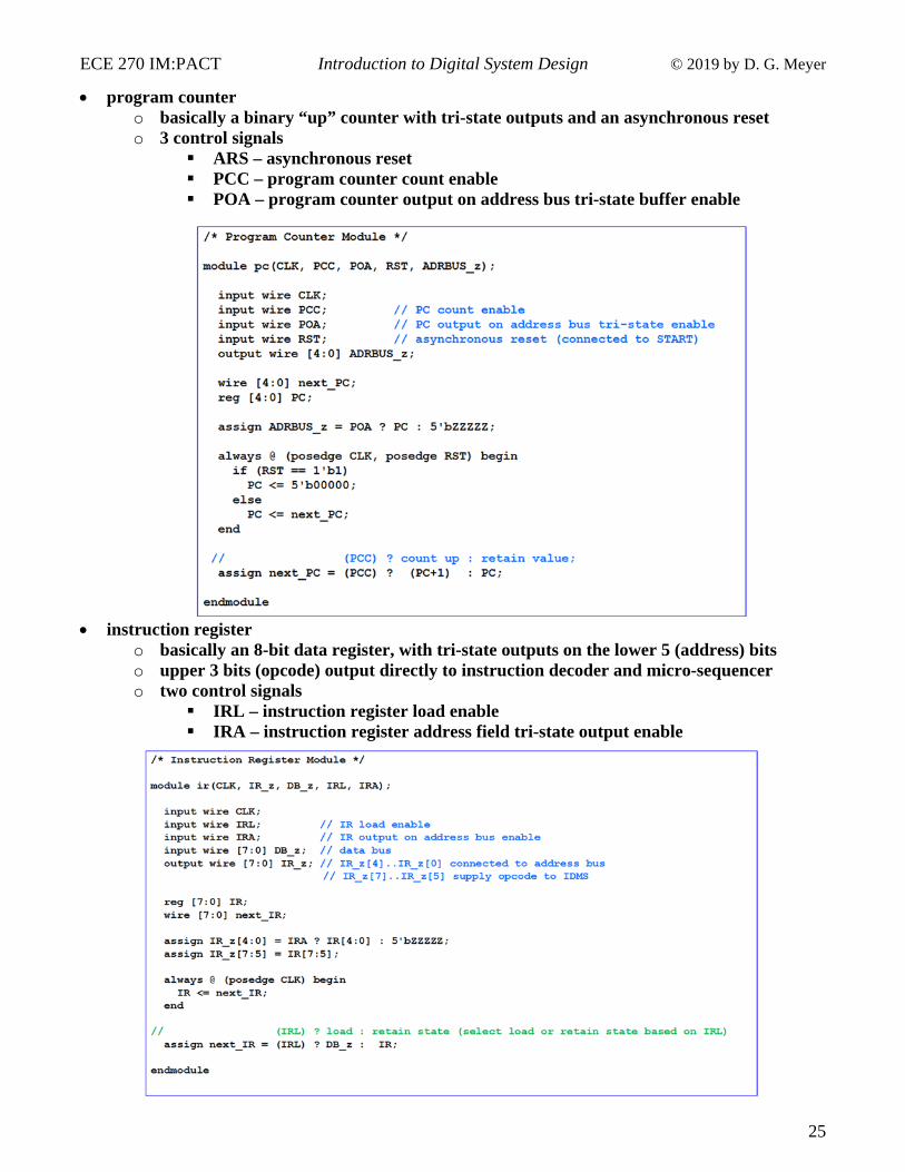
program counter o basically a binary “up” counter with tri-state outputs and an asynchronous reset o 3 control signals
ARS – asynchronous reset PCC – program counter count enable POA – program counter output on address bus tri-state buffer enable
instruction register o basically an 8-bit data register, with tri-state outputs on the lower 5 (address) bits o upper 3 bits (opcode) output directly to instruction decoder and micro-sequencer o two control signals
IRL – instruction register load enable IRA – instruction register address field tri-state output enable

ECE 270 IM:PACT Introduction to Digital System Design © 2019 by D. G. Meyer
26
ALU o a multi-function register that performs arithmetic and logical operations o four control signals
ALE – overall ALU enable ALX – function select ALY – function select AOE – A register tri-state output enable
o block diagram of one bit

ECE 270 IM:PACT Introduction to Digital System Design © 2019 by D. G. Meyer
27

ECE 270 IM:PACT Introduction to Digital System Design © 2019 by D. G. Meyer
28

ECE 270 IM:PACT Introduction to Digital System Design © 2019 by D. G. Meyer
29
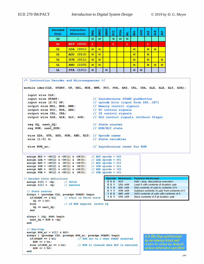
instruction decoder and microsequencer
o state machine that tells all the other state machines what to do (“orchestra director”)
o micro-sequence consists of two steps (states)
fetching instruction from memory executing instruction fetch/execute state represented by single flip-flop (SQ)
o fetch cycle
POA (output location of instruction on address bus) MSL (select memory, i.e., enable memory to participate) MOE (turn on memory tri-state buffers, so that selected location can be read) IRL (enable IR to load instruction fetched from memory) PCC (enable PC to increment)
o execute cycle – ALU functions (ADD, SUB, LDA, AND)
IRA (output operand location on address bus) MSL (select memory) MOE (enable memory to be read) ALE (enable ALU to perform the selected function)
o execute cycle – STA instruction
IRA (output location at which to store result) MSL (select memory) MWE (enable write to memory) AOE (output data in A register via data bus to memory)
o to stop execution (“halt”), need a “run/stop” flip-flop
when START pressed, asynchronously set RUN flip-flip when HLT instruction executed, asynchronously clear RUN flip-flop AND the RUN signal with each synchronous enable signal effectively disables
all functional blocks
The synchronous fetch functions (IRL and PCC) will take place on the clock edge that causes the state counter to transition from the fetch state to the execute state
ECE 270 IM:PACT Introduction to Digital System Design © 2019 by D. G. Meyer
30
ECE 270 IM:PACT Introduction to Digital System Design © 2019 by D. G. Meyer
31
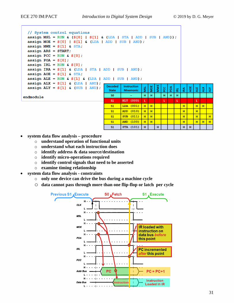
system data flow analysis – procedure
o understand operation of functional units o understand what each instruction does o identify address & data source/destination o identify micro-operations required o identify control signals that need to be asserted o examine timing relationship
system data flow analysis - constraints o only one device can drive the bus during a machine cycle o data cannot pass through more than one flip-flop or latch per cycle

ECE 270 IM:PACT Introduction to Digital System Design © 2019 by D. G. Meyer
32
ECE 270 IM:PACT Introduction to Digital System Design © 2019 by D. G. Meyer
33
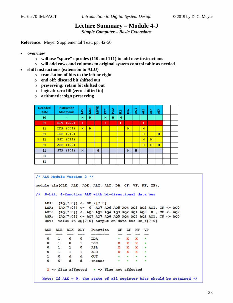
Lecture Summary – Module 4-J Simple Computer – Basic Extensions
Reference: Meyer Supplemental Text, pp. 42-50 overview
o will use “spare” opcodes (110 and 111) to add new instructions o will add rows and columns to original system control table as needed
shift instructions (extension to ALU) o translation of bits to the left or right o end off: discard bit shifted out o preserving: retain bit shifted out o logical: zero fill (zero shifted in) o arithmetic: sign preserving

ECE 270 IM:PACT Introduction to Digital System Design © 2019 by D. G. Meyer
34
input wire CLK; // ALU control lines input wire ALE; // Overall ALU enable input wire AOE; // Data bus tri-state output enable input wire ALX, ALY; // Function select inout wire [7:0] DB_z; // Bidirectional 8-bit data bus output reg CF, VF, NF, ZF; // Condition code bits (flags) // Carry, Overflow, Negative, Zero // Combinational ALU outputs wire [7:0] ALU; // Accumulator (A) register reg [7:0] AQ; // Next state variables reg next_CF, next_VF, next_NF, next_ZF; reg [7:0] next_AQ; // Combinational ALU outputs always @ (ALX, ALY, DB_z) begin case ({ALX,ALY}) 2'b00: ALU = DB_z; // LDA 2'b01: ALU = {1'b0,AQ[7:1]}; // LSR 2'b10: ALU = {AQ[6:0],1'b0}; // ASL 2'b11: ALU = {AQ[7],AQ[7:1]}; // ASR endcase end // Register bit and data bus control equations always @(posedge CLK) begin AQ <= next_AQ; end always @ (ALE, ALU, AQ) begin next_AQ = ALE ? ALU : AQ; end assign DB_z = AOE ? AQ : 8'bZZZZZZZZ; // Flag register state equations always @ (posedge CLK) begin CF <= next_CF; ZF <= next_ZF; NF <= next_NF; VF <= next_VF; end always @ (ALE, ALX, ALY, CF, ZF, NF, VF, ALU, AQ) begin casez ({ALE,ALX,ALY}) 3'b0??: next_CF = 1'b0; 3'b100: next_CF = CF; // LDA (not affected) 3'b101: next_CF = AQ[0]; // LSR 3'b110: next_CF = AQ[7]; // ASL 3'b111: next_CF = AQ[0]; // ASR endcase next_ZF = ALE ? (ALU == 0) : ZF; next_NF = ALE ? ALU[7] : NF; next_VF = VF; // NOTE: NOT AFFECTED end endmodule

ECE 270 IM:PACT Introduction to Digital System Design © 2019 by D. G. Meyer
35

ECE 270 IM:PACT Introduction to Digital System Design © 2019 by D. G. Meyer
36
input/output (I/O) instructions o new instructions
IN addr – input data from port addr and load into A register OUT addr – output data in A register to port addr
o new control signals IOR – asserted when IN executed IOW – asserted when OUT executed
o modified block diagram, Verilog code for I/O module, modified system control table
ECE 270 IM:PACT Introduction to Digital System Design © 2019 by D. G. Meyer
37
ECE 270 IM:PACT Introduction to Digital System Design © 2019 by D. G. Meyer
38
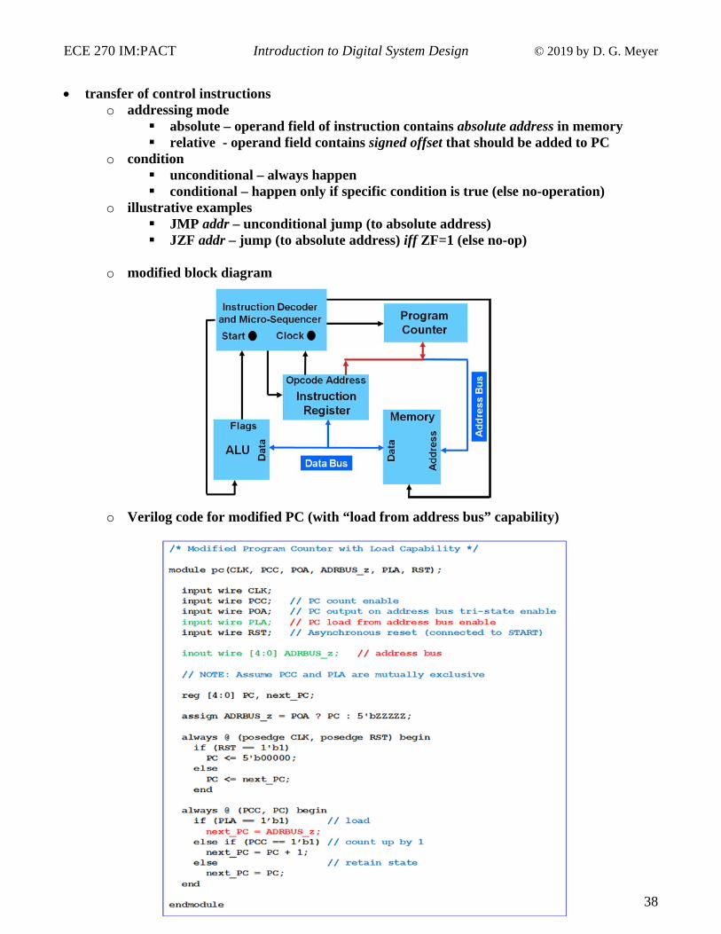
transfer of control instructions
o addressing mode absolute – operand field of instruction contains absolute address in memory relative - operand field contains signed offset that should be added to PC
o condition unconditional – always happen conditional – happen only if specific condition is true (else no-operation)
o illustrative examples JMP addr – unconditional jump (to absolute address) JZF addr – jump (to absolute address) iff ZF=1 (else no-op)
o modified block diagram
o Verilog code for modified PC (with “load from address bus” capability)
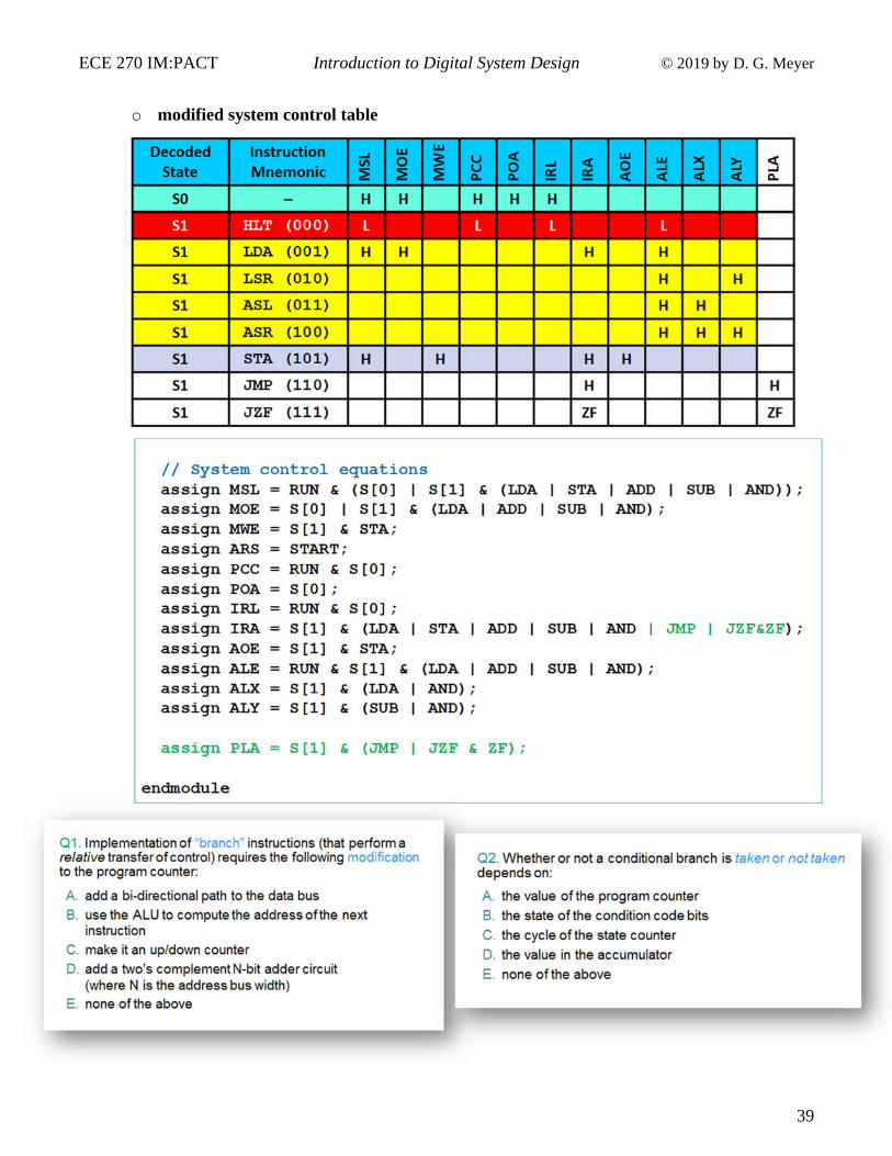
ECE 270 IM:PACT Introduction to Digital System Design © 2019 by D. G. Meyer
39
o modified system control table
ECE 270 IM:PACT Introduction to Digital System Design © 2019 by D. G. Meyer
40
Lecture Summary – Module 4-K Simple Computer – Advanced Extensions
Reference: Meyer Supplemental Text, pp. 50-64 overview
o advanced extensions include multi-cycle execution stack mechanism
state counter modifications o provide multiple execute cycles (here, up to 3) o determine number of execute cycles based on opcode o realize using 2-bit synchronously resettable state counter [SQB SQA] o new state names
S0 – fetch S1..S3 – execute (first, second, third)
o new control signal: RST (asserted on final execute state of each instruction)

ECE 270 IM:PACT Introduction to Digital System Design © 2019 by D. G. Meyer
41
/* Instruction Decoder and Microsequencer with Multi-Execution States */ module idmsr(CLK, START, OP, MSL, MOE, MWE, PCC, POA, ARS, IRL, IRA, ALE, ALX, ALY, AOE); input wire CLK; input wire START; // Asynchronous START pushbutton input wire [2:0] OP; // opcode bits (input from IR5..IR7) output wire MSL, MOE, MWE; // Memory control signals output wire PCC, POA, ARS; // PC control signals output wire IRL, IRA; // IR control signals output wire ALE, ALX, ALY, AOE; // ALU control signals reg SQA, SQB; // State counter low bit, high bit reg RUN; // RUN/HLT state wire RST; // Synchronous state counter reset wire LDA, STA, ADD, SUB, AND, HLT; wire [3:0] S; reg next_SQA, next_SQB; wire RUN_ar; // Asynchronous reset for RUN // Decoded opcode definitions assign HLT = ~OP[2] & ~OP[1] & ~OP[0]; // HLT opcode = 000 assign LDA = ~OP[2] & ~OP[1] & OP[0]; // LDA opcode = 001 assign ADD = ~OP[2] & OP[1] & ~OP[0]; // ADD opcode = 010 assign SUB = ~OP[2] & OP[1] & OP[0]; // SUB opcode = 011 assign AND = OP[2] & ~OP[1] & ~OP[0]; // AND opcode = 100 assign STA = OP[2] & ~OP[1] & OP[0]; // STA opcode = 101 // Decoded state definitions assign S[0] = ~SQB & ~SQA; // fetch state assign S[1] = ~SQB & SQA; // first execute state assign S[2] = SQB & ~SQA; // second execute state assign S[3] = SQB & SQA; // third execute state // State counter always @ (posedge CLK, posedge START) begin if(START == 1'b1) begin // start in fetch state SQA <= 1'b0; SQB <= 1'b0; end else begin SQA <= next_SQA; SQB <= next_SQB; end end always @ (RST, RUN, SQA, SQB) begin next_SQA = ~RST & RUN & ~SQA; // if RUN negated or RST asserted, next_SQB = ~RST & RUN & (SQA ^ SQB); // state counter is reset end assign RUN_ar = S[1] & HLT; // Run/stop always @ (posedge CLK, posedge RUN_ar, posedge START) begin if(START == 1'b1) // start with RUN set to 1 RUN <= 1'b1; else if(RUN_ar == 1'b1) // RUN is cleared when HLT is executed RUN <= 1'b0; end // System control equations assign MSL = RUN & (S[0] | S[1] & (LDA | STA | ADD | SUB | AND)); assign MOE = S[0] | S[1] & (LDA | ADD | SUB | AND); assign MWE = S[1] & STA; assign ARS = START; assign PCC = RUN & S[0]; assign POA = S[0]; assign IRL = RUN & S[0]; assign IRA = S[1] & (LDA | STA | ADD | SUB | AND); assign AOE = S[1] & STA; assign ALE = RUN & S[1] & (LDA | ADD | SUB | AND); assign ALX = S[1] & (LDA | AND); assign ALY = S[1] & (SUB | AND); assign RST = S[1] & (LDA | STA | ADD | SUB | AND); endmodule
ECE 270 IM:PACT Introduction to Digital System Design © 2019 by D. G. Meyer
42
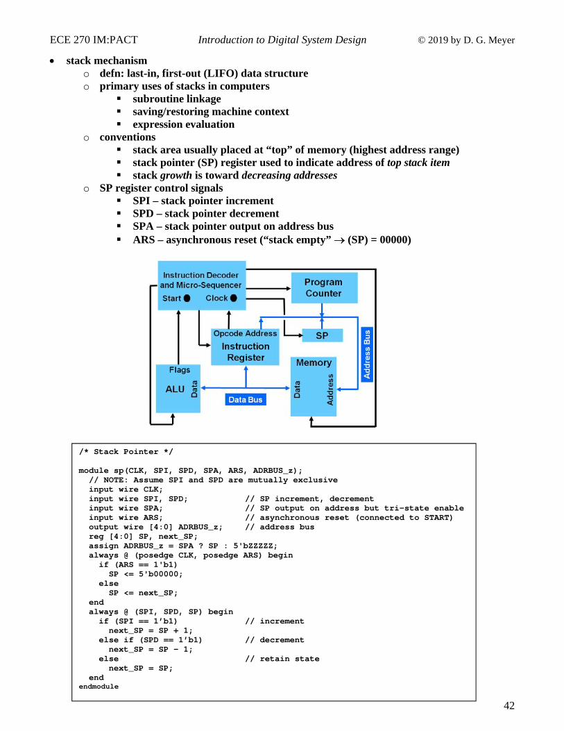
stack mechanism o defn: last-in, first-out (LIFO) data structure o primary uses of stacks in computers
subroutine linkage saving/restoring machine context expression evaluation
o conventions stack area usually placed at “top” of memory (highest address range) stack pointer (SP) register used to indicate address of top stack item stack growth is toward decreasing addresses
o SP register control signals SPI – stack pointer increment SPD – stack pointer decrement SPA – stack pointer output on address bus ARS – asynchronous reset (“stack empty” (SP) = 00000)
/* Stack Pointer */ module sp(CLK, SPI, SPD, SPA, ARS, ADRBUS_z); // NOTE: Assume SPI and SPD are mutually exclusive input wire CLK; input wire SPI, SPD; // SP increment, decrement input wire SPA; // SP output on address but tri-state enable input wire ARS; // asynchronous reset (connected to START) output wire [4:0] ADRBUS_z; // address bus reg [4:0] SP, next_SP; assign ADRBUS_z = SPA ? SP : 5'bZZZZZ; always @ (posedge CLK, posedge ARS) begin if (ARS == 1'b1) SP <= 5'b00000; else SP <= next_SP; end always @ (SPI, SPD, SP) begin if (SPI == 1’b1) // increment next_SP = SP + 1; else if (SPD == 1’b1) // decrement next_SP = SP - 1; else // retain state next_SP = SP; end endmodule

ECE 270 IM:PACT Introduction to Digital System Design © 2019 by D. G. Meyer
43
stack mechanism, continued… o new instructions understand this notation
PSH – save (A) on stack (SP) (SP) – 1 SPD ((SP)) (A) SPA, MSL, MWE, AOE
POP – load A with value of top stack item (A) ((SP)) (SP) (SP) + 1
o note the overlap of operations (single execute state) possible with “POP”
SPA, MSL, MOE, ALE, ALX, SPI

ECE 270 IM:PACT Introduction to Digital System Design © 2019 by D. G. Meyer
44
subroutine linkage o capabilities provided
arbitrary nesting of subroutine calls passing parameters to subroutine recursion reentrancy
o new instructions understand this notation JSR addr – jump to subroutine at location addr
(SP) (SP) – 1 SPD ((SP)) (PC) SPA, MSL, MWE, POD (PC) (IR5..0) IRA,PLA
RTS – return from subroutine (PC) ((SP)) (SP) (SP) + 1
note the overlap of operations (single execute state) possible with “RTS” o need PC with bi-directional data bus interface
SPA, MSL, MOE, PLD, SPI note: value loaded into PC truncated to 5 bits

ECE 270 IM:PACT Introduction to Digital System Design © 2019 by D. G. Meyer
45
/* Program Counter with Data Bus interface */ module pc(CLK, PCC, PLA, POA, RST, ADRBUS_z, DB_z, PLD, POD, PC); input wire CLK; input wire PCC; // PC count enable input wire PLA; // PC load from address bus enable input wire POA; // PC output on address bus tri-state enable input wire RST; // Asynchronous reset (connected to START) input wire PLD; // PC load from data bus enable input wire POD; // PC output on data bus tri-state enable inout wire [4:0] ADRBUS_z; // address bus (5-bits wide) inout wire [7:0] DB_z; // data bus (8-bits wide) output reg [4:0] PC; // PC register reg [4:0] next_PC; always @ (posedge CLK, posedge RST) begin if (RST == 1'b1) PC <= 5'b00000; else PC <= next_PC; end always @ (PLA, PLD, PCC, ADRBUS_z, DB_z, PC) begin // synchronous control signals PLA, PLD, and PCC are mutually exclusive if (PLA == 1’b1) // load PC from address bus next_PC = ADRBUS_z; else if (PLD == 1’b1) // load PC from data bus next_PC = DB_z; else if (PCC == 1’b1) // increment PC next_PC = PC + 1; else // retain state next_PC = PC; end assign ADRBUS_z = POA ? PC[4:0] : 5'bZZZZZ; assign DB_z = POD ? {3'b000, PC[4:0]} : 8'bZZZZZZZZ; // pad upper 3 bits of DB w/ 0 endmodule
// System control equations assign MSL = RUN & (S[0] | S[1] & (LDA | STA | ADD | SUB | AND | RTS) | S[2] & JSR); assign MOE = S[0] | S[1] & (LDA | ADD | SUB | AND | RTS); assign MWE = S[1] & STA | S[2] & JSR; assign ARS = START; assign PCC = RUN & S[0]; assign POA = S[0]; assign PLA = S[3] & JSR; assign POD = S[2] & JSR; assign PLD = S[1] & RTS; assign IRL = RUN & S[0]; assign IRA = S[1] & (LDA | STA | ADD | SUB | AND); assign AOE = S[1] & STA; assign ALE = RUN & S[1] & (LDA | ADD | SUB | AND); assign ALX = S[1] & (LDA | AND); assign ALY = S[1] & (SUB | AND); assign SPI = S[1] & RTS; assign SPD = S[1] & JSR; assign SPA = S[1] & RTS | S[2] & JSR; assign RST = S[1] & (LDA | STA | ADD | SUB | AND | RTS) | S[3] & JSR; endmodule
ECE 270 IM:PACT Introduction to Digital System Design © 2019 by D. G. Meyer
46
Fun things to think about… what kinds of new instructions would be useful in writing “real” programs? what new kinds of registers would be good to add to the machine? what new kinds of addressing modes would be nice to have? what would we have to change if we wanted “branch” transfer-of-control instructions
instead of “jump” instructions?