Embed Size (px)
Citation preview
Level Shifter Design for Voltage Stacking
Elnaz Ebrahimi, Rafael Trapani Possignolo and Jose RenauDept. of Computer Engineering, University of California, Santa Cruz, Santa Cruz, CA, 95064
Email:{eebrahim,rpossign,renau}@ucsc.edu
Abstract—As chips increase in complexity with ever increasingpower consumption, pressure in efficient power delivery mecha-nism such as multi-VDD, voltage stacked and DVS continues torise. The main objective is to reduce the overall current deliveredto the chip. For instance, in voltage stacking, if the circuit isstacked in 2 levels and supply voltage is doubled, the currentdrawn will be reduced by half. Hence, the same amount ofpower is delivered, but with half the current. With the prevalenceof systems using those techniques, level shifters will have to beoptimally designed to perform fast with low power. As the numberof level shifters grows, area consumption becomes another designfactor. This study explores different types of existing level shiftersfor voltage stacking application, their optimal sizing and energy,delay and area trade-offs. It includes effect the of PVT variationas another design factor and its impact on delay and energyconsumption. We will also propose modifications to the bestenergy-delay level shifter to reduce its area overhead.
I. INTRODUCTIONAs device size scales down and number of transistors and
frequency increase, power consumption becomes a criticalissue in System-On-Chip design. Since dynamic power iscubically proportional to supply voltage, one prevalent tech-nique to reduce power is scaling down the supply voltage,which impacts performance by reducing the frequency atwhich the design can run. To avoid performance degradation,one solution is to use multiple supply voltages to reducethe power consumption. The critical path components willcontinue running at the VDD level while non-critical pathcomponents run at a scaled down VDD [10].
Using a multi-VDD system is an alternative to voltagescaling technique. It counteracts the negative impact on per-formance, because the critical path components will continuerunning at V DD level while non-critical components run ata scaled down V DD [14]. In a multi-VDD system, when theDC current flows from a low voltage gate to a high voltagegate, the voltage is not sufficient to turn the PMOS “ON‘” andtherefore, the PMOS in the high voltage gate is weakly “ON‘”conducting static current from the power supply to the ground.The level shifters will remove the static current and restore thefull voltage swing from VddL to VddH [7].
Designing a multi-VDD system is inherently complex asthere are a few challenges in using level shifters (LS) in thesystem. They dissipate power and add propagation delay. It isnecessary to optimize the LS circuit for minimum energy-delayproduct to obtain the potential benefit of using multiple powersupply domains. As an LS includes both high voltage and lowvoltage gate, it will require more area and routing resources.For example, when each functional block on a die needs adifferent voltage for its desired performance, the number oflevel converters can easily grow and become a design areaoverhead. Techniques such as Dynamic Voltage scaling (DVS)has been widely used in digital signal processing elementsfor reducing energy consumption [17]. And future low-powersystems-on-chips (SoCs) are likely to consist of many scalablevoltage domains. This requires level shifters to be able toperform at a high speed with low power [14], [19].
Another more recent approach to reduce the current re-quired by a chip is voltage stacking [5], [11]. Voltage stacking
is connecting logic blocks in a series configuration, ratherthan parallel configuration [2], and thus delivering the sameamount of power by increasing voltage and reducing currentby a factor of n (the number of stack levels). Voltage stackinghas been proposed between cores [11], within a core [2], andmore recently in GPUs [18] and SRAMs [4]. Voltage stackingreduces the number of pins dedicated to power, increases thevoltage regulator efficiency and reduces voltage noise anddroop [2].
As in the case of multi-VDD systems, voltage stacked sys-tems require level shifters for inter-level communication [5],[11]. Traditional level shifters are inserted to translate or shiftthe logic levels from the level supplied by one domain toanother level supplied by the second domain. In the contextof voltage stacking, the level shifters will have a primaryvoltage rail which sits at the top and a secondary voltagerail which sits in the middle. When placed in a voltagestacked design, they will shift the both rails, either from GND-midrail to midrail-toprail (low to high level shifters) or frommidrail-toprail to GND-midrail (high to low level shifters).Although many designs for level shifters exist, an evaluationof different designs in the context of voltage stacking hasnot been made, so the trade-offs of different designs are notclear. We evaluate existing approaches of LSs for voltagestacking applications. We are especially interested in delayand power, but area and sensitivity to PVT (Process, Voltageand Temperature) variations are also considered. Each of thoseparameters may have different priority in different designs. Forinstance, CoreUnfolding [2] allows an entire clock cycle forlevel shifting, thus delay is less important. However, it requiresa large amount of shifters, which makes area a critical designfactor. On the other hand, a voltage stacked SRAM [4] requiresminimal impact on timing, but due to the small number ofshifters, can tolerate more area overhead per shifter.
The contributions of this paper are:• Overview of different LS designs.• Energy, delay, and area comparison of LS designs.• PVT tolerance evaluation of LS designs.
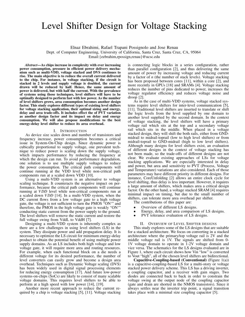
II. OVERVIEW OF LEVEL SHIFTER DESIGNSThis study explores some of the LS designs that are suitable
for a stacked architecture. We focus on converting in a stackedarchitecture where the primary/top voltage rail is 2V and themiddle voltage rail is 1V. The signals are shifted from 0-1V voltage domain to operate in 1-2V voltage domain andvice versa. The schematics for the LS designs evaluated are inFigure 1, where each circuit shows how Vin “low” is convertedto Vout “high”, all of the chosen level shifters are bidirectional.
Capacitive-Coupling-based (Conventional) (Figure 1(a))is a capacitive-coupling-based LS for a multi-story or voltagestacked power delivery scheme. This LS has a driving inverter,a coupling capacitor, and a receiver with gain stages. Twodiodes are connected back to back in order to constrain thevoltage swing at the output node of the coupling capacitor(gate and drain are shorted in the NMOS transistors). Since italways settles near the inverter trip point, a signal transitiontakes place with a minimal size coupling capacitor [5].
Two-Stage Cross-Coupled (TSCC) (Figure 1(b)) uses twocross-coupled stages. The first stage is a differential cascadevoltage switched logic gate, using a cross-coupled PMOS halflatch operating at the higher supply voltage. To overcome theleakage of weakly conducting PMOS transistors, drive strengthof NMOS transistor is enhanced. Low Vin input voltage turnsmn1 on, which discharges node A to ground and activates mp2.Node B will be pulled up to VddH and the output voltagewill be low. Subsequently, when Vin is asserted, mn2 andmp1 are activated shifting the output voltage up to VddH.The drive of the pull-down transistors needs to be much largerthan the PMOS transistors to overcome its latch action drivenwith a higher supply voltage. It is a simple design suited forsuper-threshold conversion [6], [8], [12]. The second stage isintended to achieve full voltage swing. The diode-connectedNMOS transistor is employed to weaken the pull-up network(Figure 1(c)), which expands the convertible input voltage.The operating range is determined by the transistor size andthreshold voltage [8], [9], [19].
Wilson Current Mirror (WCM) (Figure 1(c)) is basedon the traditional Current Mirror (CM), a unity gain currentamplifier which provides output current proportional to inputcurrent at its high impedance output. It maintains the outputcurrent constant regardless of load [1], [12]. The high drain-to-source voltage of PMOSs facilitates the construction of astable current mirror, which offers an effective on-off currentcomparison at the output. However, for super-threshold inputvoltage, a high amount of quiescent current occurs, limitingthe its use [8]. In WCM, this current is cut off by a feedbackPMOS (mp3), reducing standby power. However, as the sourcecurrent is cut off, the mirror current through mp2 is largelyreduced, weakening pull-up strength and dropping the voltageat node A. Although the voltage drop increases the sourcecurrent through the feedback control, the current increase istoo small to pull the voltage at node A back to VddH. Theoutput finally stabilizes at a voltage below VddH, which causeslarge static current and standby power in the output buffer [19].
Stacked Wilson Current Mirror (Stacked) (Figure 1(d))is an enhancement to the WCM design and Kumar et al. usea stacking technique to reduce the leakage power consump-tion [13]. The technique adds three NMOS transistors in thepull-down network.
Switched-Capacitance (Tong) (Figure 1(e)) is acapacitive-coupled design for voltage stacking [11]. Thevoltage across the capacitor depends on the differencebetween the two domains ,but it can be higher than thegate-oxide breakdown voltage. Hence, this approach requiresmetaloxidemetal (MOM) capacitors [16]. The original designhas one 25fF capacitor on each side of the back to backinverters. If we translate each fF to ≈ 1um2, the LS areais considerably large. Our experiments show that the 25fFcapacitors are over-designed for an LS, and we were able toreduce that number to ≈2.6fF (details in the experimentalsection), considering a 30% margin over the minimumoperational point. Even with this size reduction, the area isstill large.
Modified Switched-Cap (Mod-Tong) (Figure 1(f)): Toprevent the use of the MOM capacitors in Tong, we replaceeach capacitor with two NMOS transistors connected such thatthe drain and gate are shorted. This reduces the area, but isexpected to increase the power consumption due to the resistiveeffect added.
III. CHARACTERIZATIONA. Transistor Sizing
To setup LSs for energy, delay, and area comparison,we begin by determining the optimal size for each LS. Our
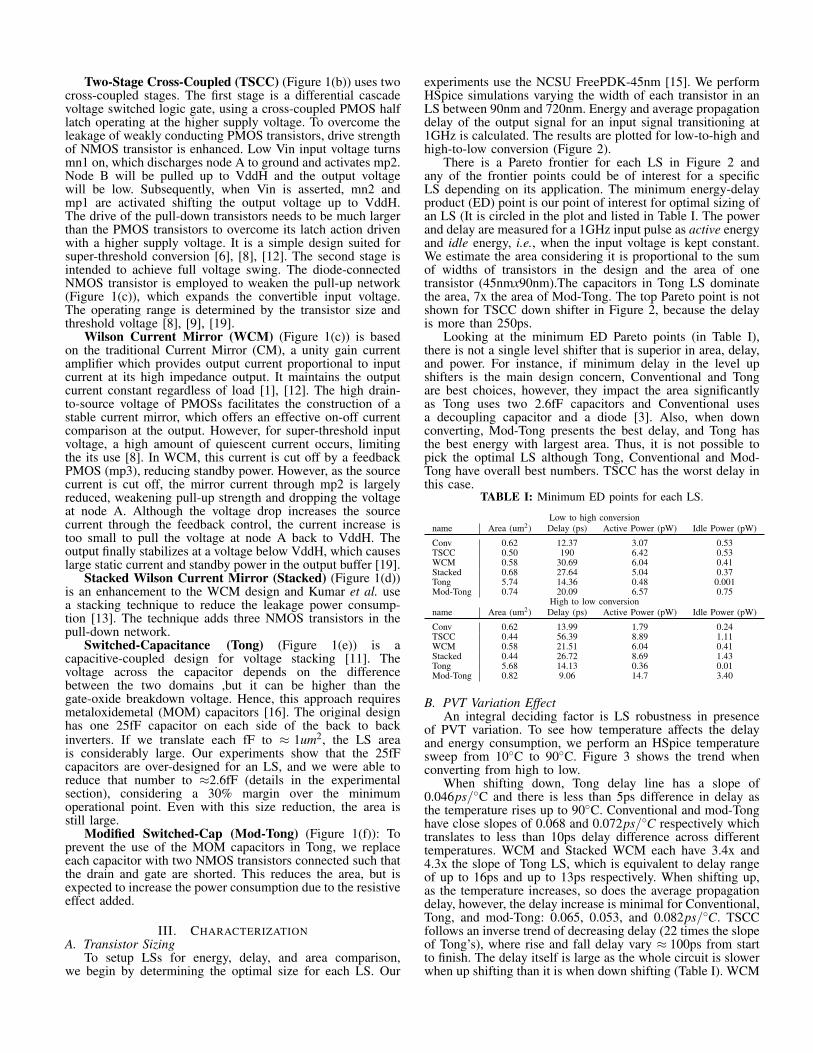
experiments use the NCSU FreePDK-45nm [15]. We performHSpice simulations varying the width of each transistor in anLS between 90nm and 720nm. Energy and average propagationdelay of the output signal for an input signal transitioning at1GHz is calculated. The results are plotted for low-to-high andhigh-to-low conversion (Figure 2).
There is a Pareto frontier for each LS in Figure 2 andany of the frontier points could be of interest for a specificLS depending on its application. The minimum energy-delayproduct (ED) point is our point of interest for optimal sizing ofan LS (It is circled in the plot and listed in Table I. The powerand delay are measured for a 1GHz input pulse as active energyand idle energy, i.e., when the input voltage is kept constant.We estimate the area considering it is proportional to the sumof widths of transistors in the design and the area of onetransistor (45nmx90nm).The capacitors in Tong LS dominatethe area, 7x the area of Mod-Tong. The top Pareto point is notshown for TSCC down shifter in Figure 2, because the delayis more than 250ps.
Looking at the minimum ED Pareto points (in Table I),there is not a single level shifter that is superior in area, delay,and power. For instance, if minimum delay in the level upshifters is the main design concern, Conventional and Tongare best choices, however, they impact the area significantlyas Tong uses two 2.6fF capacitors and Conventional usesa decoupling capacitor and a diode [3]. Also, when downconverting, Mod-Tong presents the best delay, and Tong hasthe best energy with largest area. Thus, it is not possible topick the optimal LS although Tong, Conventional and Mod-Tong have overall best numbers. TSCC has the worst delay inthis case.
TABLE I: Minimum ED points for each LS.
Low to high conversionname Area (um2) Delay (ps) Active Power (pW) Idle Power (pW)
Conv 0.62 12.37 3.07 0.53TSCC 0.50 190 6.42 0.53WCM 0.58 30.69 6.04 0.41Stacked 0.68 27.64 5.04 0.37Tong 5.74 14.36 0.48 0.001Mod-Tong 0.74 20.09 6.57 0.75
High to low conversionname Area (um2) Delay (ps) Active Power (pW) Idle Power (pW)
Conv 0.62 13.99 1.79 0.24TSCC 0.44 56.39 8.89 1.11WCM 0.58 21.51 6.04 0.41Stacked 0.44 26.72 8.69 1.43Tong 5.68 14.13 0.36 0.01Mod-Tong 0.82 9.06 14.7 3.40
B. PVT Variation EffectAn integral deciding factor is LS robustness in presence
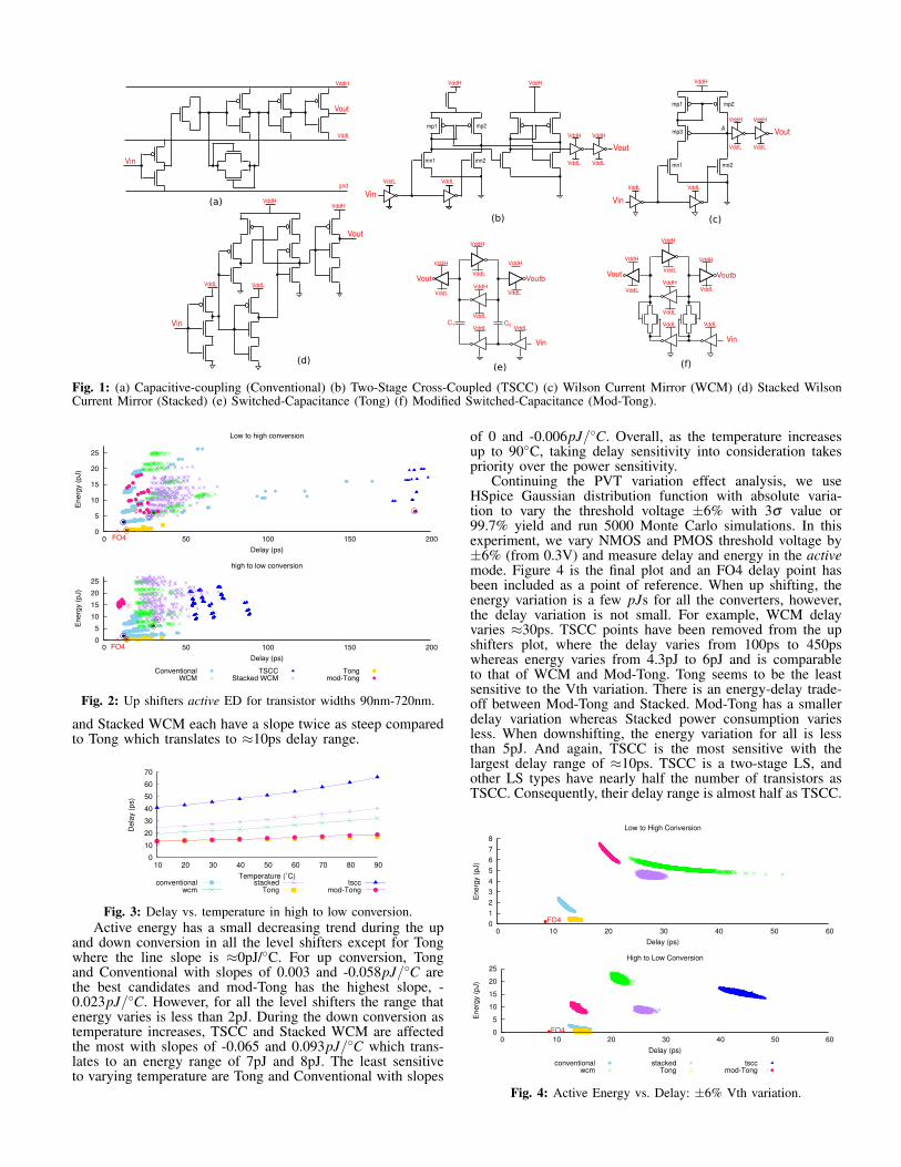
of PVT variation. To see how temperature affects the delayand energy consumption, we perform an HSpice temperaturesweep from 10◦C to 90◦C. Figure 3 shows the trend whenconverting from high to low.
When shifting down, Tong delay line has a slope of0.046ps/◦C and there is less than 5ps difference in delay asthe temperature rises up to 90◦C. Conventional and mod-Tonghave close slopes of 0.068 and 0.072ps/◦C respectively whichtranslates to less than 10ps delay difference across differenttemperatures. WCM and Stacked WCM each have 3.4x and4.3x the slope of Tong LS, which is equivalent to delay rangeof up to 16ps and up to 13ps respectively. When shifting up,as the temperature increases, so does the average propagationdelay, however, the delay increase is minimal for Conventional,Tong, and mod-Tong: 0.065, 0.053, and 0.082ps/◦C. TSCCfollows an inverse trend of decreasing delay (22 times the slopeof Tong’s), where rise and fall delay vary ≈ 100ps from startto finish. The delay itself is large as the whole circuit is slowerwhen up shifting than it is when down shifting (Table I). WCM
Vin
VddH
VddL
Vout
gnd
(a)
Vin
VddL
Voutb
VddH
VddLVout
C1 C2
VddL
VddHVddH
VddL
VddL
VddHVddL
(e)
VddL
Vin
VddL
Voutb
VddH
VddLVout
VddL
VddH
VddL
VddH
VddL
VddH
(f)
Vin
Vout
VddH
VddL VddL
VddH
(d)
Vin
Vout
VddH
VddL
VddH VddH
VddL VddL
VddL
(c)
mn1 mn2
mp2mp1
mp3A
mn1 mn2
mp2mp1
Vin
Vout
VddH
VddL
VddH VddH
VddH
VddL
VddL VddL
(b)
Fig. 1: (a) Capacitive-coupling (Conventional) (b) Two-Stage Cross-Coupled (TSCC) (c) Wilson Current Mirror (WCM) (d) Stacked WilsonCurrent Mirror (Stacked) (e) Switched-Capacitance (Tong) (f) Modified Switched-Capacitance (Mod-Tong).
0
5
10
15
20
25
0 50 100 150 200
En
erg
y (
pJ)
Delay (ps)
Low to high conversion
FO4
0
5
10
15
20
25
0 50 100 150 200
En
erg
y (
pJ)
Delay (ps)
high to low conversion
ConventionalWCM
TSCCStacked WCM
Tongmod-Tong
FO4
Fig. 2: Up shifters active ED for transistor widths 90nm-720nm.
and Stacked WCM each have a slope twice as steep comparedto Tong which translates to ≈10ps delay range.
0
10
20
30
40
50
60
70
10 20 30 40 50 60 70 80 90
Dela
y (
ps)
Temperature (˚C)conventional
wcmstacked
Tongtscc
mod-Tong
Fig. 3: Delay vs. temperature in high to low conversion.Active energy has a small decreasing trend during the up
and down conversion in all the level shifters except for Tongwhere the line slope is ≈0pJ/◦C. For up conversion, Tongand Conventional with slopes of 0.003 and -0.058pJ/◦C arethe best candidates and mod-Tong has the highest slope, -0.023pJ/◦C. However, for all the level shifters the range thatenergy varies is less than 2pJ. During the down conversion astemperature increases, TSCC and Stacked WCM are affectedthe most with slopes of -0.065 and 0.093pJ/◦C which trans-lates to an energy range of 7pJ and 8pJ. The least sensitiveto varying temperature are Tong and Conventional with slopes
of 0 and -0.006pJ/◦C. Overall, as the temperature increasesup to 90◦C, taking delay sensitivity into consideration takespriority over the power sensitivity.
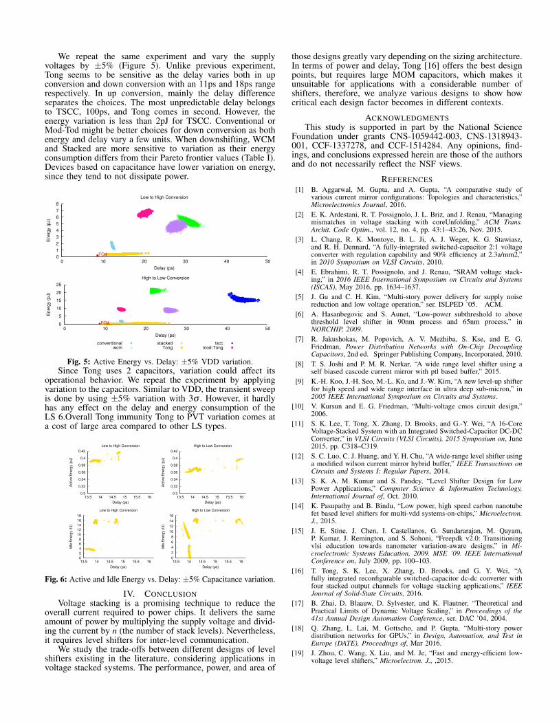
Continuing the PVT variation effect analysis, we useHSpice Gaussian distribution function with absolute varia-tion to vary the threshold voltage ±6% with 3σ value or99.7% yield and run 5000 Monte Carlo simulations. In thisexperiment, we vary NMOS and PMOS threshold voltage by±6% (from 0.3V) and measure delay and energy in the activemode. Figure 4 is the final plot and an FO4 delay point hasbeen included as a point of reference. When up shifting, theenergy variation is a few pJs for all the converters, however,the delay variation is not small. For example, WCM delayvaries ≈30ps. TSCC points have been removed from the upshifters plot, where the delay varies from 100ps to 450pswhereas energy varies from 4.3pJ to 6pJ and is comparableto that of WCM and Mod-Tong. Tong seems to be the leastsensitive to the Vth variation. There is an energy-delay trade-off between Mod-Tong and Stacked. Mod-Tong has a smallerdelay variation whereas Stacked power consumption variesless. When downshifting, the energy variation for all is lessthan 5pJ. And again, TSCC is the most sensitive with thelargest delay range of ≈10ps. TSCC is a two-stage LS, andother LS types have nearly half the number of transistors asTSCC. Consequently, their delay range is almost half as TSCC.
0
1
2
3
4
5
6
7
8
0 10 20 30 40 50 60
Energ
y (
pJ)
Delay (ps)
Low to High Conversion
FO4
0
5
10
15
20
25
0 10 20 30 40 50 60
Energ
y (
pJ)
Delay (ps)
High to Low Conversion
conventionalwcm
stackedTong
tsccmod-Tong
FO4
Fig. 4: Active Energy vs. Delay: ±6% Vth variation.
We repeat the same experiment and vary the supplyvoltages by ±5% (Figure 5). Unlike previous experiment,Tong seems to be sensitive as the delay varies both in upconversion and down conversion with an 11ps and 18ps rangerespectively. In up conversion, mainly the delay differenceseparates the choices. The most unpredictable delay belongsto TSCC, 100ps, and Tong comes in second. However, theenergy variation is less than 2pJ for TSCC. Conventional orMod-Tod might be better choices for down conversion as bothenergy and delay vary a few units. When downshifting, WCMand Stacked are more sensitive to variation as their energyconsumption differs from their Pareto frontier values (Table I).Devices based on capacitance have lower variation on energy,since they tend to not dissipate power.
0
1
2
3
4
5
6
7
8
0 10 20 30 40 50
Energ
y (
pJ)
Delay (ps)
Low to High Conversion
FO4
0
5
10
15
20
25
0 10 20 30 40 50
Energ
y (
pJ)
Delay (ps)
High to Low Conversion
conventionalwcm
stackedTong
tsccmod-Tong
FO4
Fig. 5: Active Energy vs. Delay: ±5% VDD variation.Since Tong uses 2 capacitors, variation could affect its
operational behavior. We repeat the experiment by applyingvariation to the capacitors. Similar to VDD, the transient sweepis done by using ±5% variation with 3σ . However, it hardlyhas any effect on the delay and energy consumption of theLS 6.Overall Tong immunity Tong to PVT variation comes ata cost of large area compared to other LS types.
0.3
0.32
0.34
0.36
0.38
0.4
0.42
13.5 14 14.5 15 15.5 16
Active
En
erg
y (
pJ)
Delay (ps)
Low to High Conversion
0.3
0.32
0.34
0.36
0.38
0.4
0.42
13.5 14 14.5 15 15.5 16
Active
En
erg
y (
pJ)
Delay (ps)
High to Low Conversion
0
2
4
6
8
10
12
14
16
18
13.5 14 14.5 15 15.5 16
Idle
En
erg
y (
fJ)
Delay (ps)
Low to High Conversion
0
2
4
6
8
10
12
14
16
13.5 14 14.5 15 15.5 16
Idle
En
erg
y (
fJ)
Delay (ps)
High to Low Conversion
Fig. 6: Active and Idle Energy vs. Delay: ±5% Capacitance variation.
IV. CONCLUSIONVoltage stacking is a promising technique to reduce the
overall current required to power chips. It delivers the sameamount of power by multiplying the supply voltage and divid-ing the current by n (the number of stack levels). Nevertheless,it requires level shifters for inter-level communication.
We study the trade-offs between different designs of levelshifters existing in the literature, considering applications involtage stacked systems. The performance, power, and area of
those designs greatly vary depending on the sizing architecture.In terms of power and delay, Tong [16] offers the best designpoints, but requires large MOM capacitors, which makes itunsuitable for applications with a considerable number ofshifters, therefore, we analyze various designs to show howcritical each design factor becomes in different contexts.
ACKNOWLEDGMENTSThis study is supported in part by the National Science
Foundation under grants CNS-1059442-003, CNS-1318943-001, CCF-1337278, and CCF-1514284. Any opinions, find-ings, and conclusions expressed herein are those of the authorsand do not necessarily reflect the NSF views.
REFERENCES[1] B. Aggarwal, M. Gupta, and A. Gupta, “A comparative study of
various current mirror configurations: Topologies and characteristics,”Microelectronics Journal, 2016.
[2] E. K. Ardestani, R. T. Possignolo, J. L. Briz, and J. Renau, “Managingmismatches in voltage stacking with coreUnfolding,” ACM Trans.Archit. Code Optim., vol. 12, no. 4, pp. 43:1–43:26, Nov. 2015.
[3] L. Chang, R. K. Montoye, B. L. Ji, A. J. Weger, K. G. Stawiasz,and R. H. Dennard, “A fully-integrated switched-capacitor 2:1 voltageconverter with regulation capability and 90% efficiency at 2.3a/mm2,”in 2010 Symposium on VLSI Circuits, 2010.
[4] E. Ebrahimi, R. T. Possignolo, and J. Renau, “SRAM voltage stack-ing,” in 2016 IEEE International Symposium on Circuits and Systems(ISCAS), May 2016, pp. 1634–1637.
[5] J. Gu and C. H. Kim, “Multi-story power delivery for supply noisereduction and low voltage operation,” ser. ISLPED ’05. ACM.
[6] A. Hasanbegovic and S. Aunet, “Low-power subthreshold to abovethreshold level shifter in 90nm process and 65nm process,” inNORCHIP, 2009.
[7] R. Jakushokas, M. Popovich, A. V. Mezhiba, S. Kse, and E. G.Friedman, Power Distribution Networks with On-Chip DecouplingCapacitors, 2nd ed. Springer Publishing Company, Incorporated, 2010.
[8] T. S. Joshi and P. M. R. Nerkar, “A wide range level shifter using aself biased cascode current mirror with ptl based buffer,” 2015.
[9] K.-H. Koo, J.-H. Seo, M.-L. Ko, and J.-W. Kim, “A new level-up shifterfor high speed and wide range interface in ultra deep sub-micron,” in2005 IEEE International Symposium on Circuits and Systems.
[10] V. Kursun and E. G. Friedman, “Multi-voltage cmos circuit design,”2006.
[11] S. K. Lee, T. Tong, X. Zhang, D. Brooks, and G.-Y. Wei, “A 16-CoreVoltage-Stacked System with an Integrated Switched-Capacitor DC-DCConverter,” in VLSI Circuits (VLSI Circuits), 2015 Symposium on, June2015, pp. C318–C319.
[12] S. C. Luo, C. J. Huang, and Y. H. Chu, “A wide-range level shifter usinga modified wilson current mirror hybrid buffer,” IEEE Transactions onCircuits and Systems I: Regular Papers, 2014.
[13] S. K. A. M. Kumar and S. Pandey, “Level Shifter Design for LowPower Applications,” Computer Science & Information Technology,International Journal of, Oct. 2010.
[14] K. Pasupathy and B. Bindu, “Low power, high speed carbon nanotubefet based level shifters for multi-vdd systems-on-chips,” Microelectron.J., 2015.
[15] J. E. Stine, J. Chen, I. Castellanos, G. Sundararajan, M. Qayam,P. Kumar, J. Remington, and S. Sohoni, “Freepdk v2.0: Transitioningvlsi education towards nanometer variation-aware designs,” in Mi-croelectronic Systems Education, 2009. MSE ’09. IEEE InternationalConference on, July 2009, pp. 100–103.
[16] T. Tong, S. K. Lee, X. Zhang, D. Brooks, and G. Y. Wei, “Afully integrated reconfigurable switched-capacitor dc-dc converter withfour stacked output channels for voltage stacking applications,” IEEEJournal of Solid-State Circuits, 2016.
[17] B. Zhai, D. Blaauw, D. Sylvester, and K. Flautner, “Theoretical andPractical Limits of Dynamic Voltage Scaling,” in Proceedings of the41st Annual Design Automation Conference, ser. DAC ’04, 2004.
[18] Q. Zhang, L. Lai, M. Gottscho, and P. Gupta, “Multi-story powerdistribution networks for GPUs,” in Design, Automation, and Test inEurope (DATE), Proceedings of, Mar 2016.
[19] J. Zhou, C. Wang, X. Liu, and M. Je, “Fast and energy-efficient low-voltage level shifters,” Microelectron. J., ,2015.