Embed Size (px)
Citation preview
CERN LHCC 2000-037LHCb TDR 36 September 2000
LHCb
RICH Technical Design Report
Printed at CERNGeneva, 2000

This Technical Design Report is dedicated to Tom Ypsilantis. Tom conceived the RingImaging Cherenkov detectors for particle identification in LHCb and he made an inestimablecontribution to the LHCb RICH project.
Tom would have wished to see these detectors in operation. He was totally dedicated to theproject. He will be missed by the RICH group for his ideas, his guidance, his animation of groupmeetings, his criticism, always given kindly and constructively. For many he was a close friend,for all a respected colleague.
ii

The LHCb Collaboration1
University of Rio de Janeiro, UFRJ, Rio de Janeiro, BrasilS.Amato, D.Carvalho, P.Colrain, T.da Silva, J.R.T.de Mello, L.de Paula, M.Gandelman,J.Helder Lopes, B.Marechal, D.Moraes, E.Polycarpo
University of Clermont-Ferrand II, Clermond-Ferrand, FranceZ.Ajaltouni, G.Bohner, V.Breton, R.Cornat, O.Deschamps, A.Falvard, J.Lecoq, P.Perret,C.Trouilleau, A.Ziad
CPPM Marseille, Aix University-Marseille II, Marseille, FranceE.Aslanides, J.P.Cachemiche, R.Legac, O.Leroy, M.Menouni, R.Potheau, A.Tsaregorodtsev
University of Paris-Sud, LAL Orsay, Orsay, FranceG.Barrand, C.Beigbeder-Beau, D.Breton, T.Caceres, O.Callot, Ph.Cros, B.D’Almagne,B.Delcourt, F.Fulda Quenzer, A.Hrisoho, B.Jean-Marie, J.Lefrancois, V.Tocut, K.Truong
Humboldt University, Berlin, GermanyT.Lohse
Technical University of Dresden, Dresden, GermanyR.Schwierz, B.Spaan
University of Freiburg, Freiburg, GermanyH.Fischer, J.Franz, F.H.Heinsius, K.Konigsmann, H.Schmitt
Max-Planck-Institute for Nuclear Physics, Heidelberg, GermanyC.Bauer, D.Baumeister, N.Bulian, H.P.Fuchs, T.Glebe, W.Hofmann, K.T.Knopfle, S.Lochner,M.Schmelling, B.Schwingenheuer, F.Sciacca, E.Sexauer, U.Trunk
Physics Institute, University of Heidelberg, Heidelberg, GermanyS.Bachmann, P.Bock, H.Deppe, H.B.Dries, F.Eisele, M.Feuerstack-Raible, S.Henneberger,P.Igo-Kemenes, Ch.Rummel, R.Rusnyak, U.Stange
Kirchhoff Institute for Physics, University of Heidelberg, Heidelberg, GermanyV.Lindenstruth, R.Richter, M.W.Schultz, A.Walsch
Frascati Laboratori Nazionali, Frascati, ItalyG.Bencivenni, C.Bloise, F.Bossi, P.Campana, G.Capon, P.DeSimone, C.Forti, M.Murtas,L.Passalacqua, V.Patera(1), L.Satta(1), A.Sciubba(1)(1) Also at Dipartimento di Energetica, University of Rome, “La Sapienza”
University of Bologna and INFN, Bologna, ItalyM.Bargiotti, A.Bertin, M.Bruschi, M.Capponi, I.D’Antone, S.Castro,R.Dona, D.Galli,B.Giacobbe, U.Marconi, I.Massa, M.Piccinini, M.Poli, N.Semprini-Cesari, R.Spighi, V.Vagnoni,S.Vecchi, M.Villa, A.Vitale, A.Zoccoli
1This list includes additional colleagues who made particular contributions to the work presented in this TDR.
iii

University of Cagliari and INFN, Cagliari, ItalyW.Bonivento, A.Cardini, M.Caria, A.Lai, D.Pinci, B.Saitta
University of Ferrara and INFN, Ferrara, ItalyV.Carassiti, A.Cotta Ramusino, P.Dalpiaz, A.Gianoli, M.Martini, F.Petrucci, M.Savrie
University of Florence and INFN, Florence, ItalyA.Bizzeti, M.Calvetti, E.Iacopini, M.Lenti, F.Martelli, G.Passaleva, M.Veltri
University of Genoa and INFN, Genoa, ItalyS.Cuneo, F.Fontanelli, V.Gracco, P.Musico, A.Petrolini, M.Sannino
University of Milano and INFN, Milano, ItalyM.Alemi, T.Bellunato, M.Calvi, C.Matteuzzi, P.Negri, M.Paganoni, V.Verzi
University of Rome, “La Sapienza” and INFN, Rome, ItalyG.Auriemma, V.Bocci, C.Bosio, G.Chiodi, D.Fidanza, A.Frenkel, K.Harrison, S.Mari,G.Martellotti, S.Martinez, G.Penso, R.Santacesaria, C.Satriano, A.Satta
University of Rome, “Tor Vergata” and INFN, Rome, ItalyG.Carboni, D.Domenici, R.Messi, L.Pacciani, L.Paoluzi, E.Santovetti
NIKHEF, The NetherlandsT.S.Bauer(4), M.Doets(1,2), Y.Gouz(1,5), V.Gromov(1), R.Hierck(1), L.Hommels(1),E.Jans(1), T.Ketel(2), S.Klous (2), B.Koene(1), M.Merk(1), M.Needham(1),H.Schuijlenburg(1), T.Sluijk(1), L.Wiggers(1), G.van Apeldoorn(3), N.van Bakel(1,2),J.van den Brand(1), R.van der Eijk(1), N.Zaitsev(3,6)(1) Foundation of Fundamental Research of Matter in the Netherlands,(2) Free University Amsterdam,(3) University of Amsterdam,(4) University of Utrecht,(5) On leave from Protvino,(6) On leave from Petersburg
Institute of High Energy Physics, Beijing, P.R.C.C.Gao, C.Jiang, H.Sun, Z.Zhu
Research Centre of High Energy Physics, Tsinghua University, Beijing, P.R.C.M.Bisset, J.P.Cheng, Y.G.Cui, Y.Gao, H.J.He, Y.P.Kuang, Y.J.Li, Y.Liao, Q.Lin, J.P.Ni,B.B.Shao, J.J.Su, Y.R.Tian, Q.Wang, Q.S.Yan
Institute for Nuclear Physics and University of Mining and Metalurgy, Krakow,PolandE.Banas, J.Blocki, K.Galuszka, P.Jalocha, P.Kapusta, B.Kisielewski, W.Kucewicz, T.Lesiak,J.Michalowski, B.Muryn, Z.Natkaniec, W.Ostrowicz, G.Polok, E.Rulikowska-Zarebska,M.Stodulski, M.Witek, P.Zychowski
Soltan Institute for Nuclear Physics, Warsaw, Poland
iv
M.Adamus, A.Chlopik, Z.Guzik, A.Nawrot, M.Szczekowski
Horia Hulubei-National Institute for Physics and Nuclear Engineering (IFIN-HH), Bucharest-Magurele, RomaniaD.V.Anghel, C.Coca, D.Dumitru, G.Giolu, C.Magureanu, R.Petrescu, S.Popescu, T.Preda,A.M.Rosca, V.L.Rusu
Institute for Nuclear Research (INR), Moscow, RussiaV.Bolotov, S.Filippov, J.Gavrilov, E.Guschin, V.Kloubov, L.Kravchuk, S.Laptev, V.Laptev,V.Postoev, A.Sadovski, I.Semeniouk
Institute of Theoretical and Experimental Physics (ITEP), Moscow, RussiaS.Barsuk, I.Belyaev, A.Golutvin, O.Gouchtchine, V.Kiritchenko, G.Kostina, N.Levitski,A.Morozov, P.Pakhlov, D.Roussinov, V.Rusinov, S.Semenov, A.Soldatov, E.Tarkovski
P.N.Lebedev Physical Institute, Moscow, RussiaYu.Alexandrov, V.Baskov, L.Gorbov, B.Govorkov, V.Kim, P.Netchaeva, V.Polianski,L.Shtarkov, A.Verdi, M.Zavertiaev
Institute for High Energy Physics (IHEP-Serpukhov),Protvino, RussiaI.V.Ajinenko, K.Beloous, V.Brekhovskikh, S.Denissov, R.I.Dzhelyadin, A.V.Dorokhov,A.Kobelev, A.K.Konoplyannikov, A.K.Likhoded, V.D.Matveev, V.Novikov, V.F.Obraztsov,A.P.Ostankov, V.I.Rykalin, V.K.Semenov, M.M.Shapkin, N.Smirnov, M.M.Soldatov, A.Sokolov,V.V.Talanov, O.P.Yushchenko
Petersburg Nuclear Physics Institute, Gatchina, St.Petersburg, RussiaB.Botchine, S.Guetz, A.Kashchuk, V.Lazarev, N.Saguidova, V.Souvorov, E.Spiridenkov,A.Vorobyov, An.Vorobyov
University of Barcelona, Barcelona, SpainS.Botta Ferragut, L.Garrido Beltran, D.Gascon, R.Miquel, D.Peralta-Rodriguez, M.RoselloCanal(1), X.Vilasis Cardona(1)(1) Departament d’Engineria Electronica La Salle, Universitat Ramon Llull, Barcelona
University of Santiago de Compostela, Santiago de Compostela, SpainB.Adeva, P.Conde, F.Gomez, J.A.Hernando, A.Iglesias, A.Lopez-Aguera, A.Pazos, M.Plo,J.M.Rodriguez, J.J.Saborido, M.J.Tobar
University of Lausanne, Lausanne, SwitzerlandP.Bartalini, A.Bay, C.Currat, O.Dormond, F.Durrenmatt, Y.Ermoline, R.Frei, G.Gagliardi,J.P.Hertig, G.Haefeli, P.Koppenburg, J.P.Perroud, F.Ronga, O.Schneider, L.Studer, M.Tareb,M.T.Tran
University of Zurich , Zurich, SwitzerlandR.Bernet, E.Holzschuh, P.Sievers, O.Steinkamp, U.Straumann, D.Wyler, M.Ziegler
Institute of Physics and Techniques, Kharkov, UkraineS.Maznichenko, O.Omelaenko, Yu.Ranyuk, M.V.Sosipatorow
v

Institute for Nuclear Research, Kiev, UkraineV.Aushev, V.Kiva, I.Kolomiets, Yu.Pavlenko, V.Pugatch, Yu.Vasiliev, V.Zerkin
University of Bristol, Bristol, U.K.N.Brook, R.Head, F.Wilson
University of Cambridge, Cambridge, U.K.V.Gibson, S.G.Katvars, C.R.Jones, C.Shepherd-Themistocleous, C.P.Ward, D.R.Ward,S.A.Wotton
Rutherford Appleton Laboratory, Chilton, U.K.C.A.J.Brew, C.J.Densham, S.Easo, B.Franek, M.J.French, J.G.V.Guy, R.N.J.Halsall,J.A.Lidbury, J.V.Morris, A.Papanestis, G.N.Patrick, F.J.P.Soler, S.A.Temple
University of Edinburgh, Edinburgh, U.K.S.Eisenhardt, A.Khan, F.Muheim, S.Playfer, A.Walker
University of Glasgow, Glasgow, U.K.A.J.Flavell, A.Halley, V.O’Shea, F.J.P.Soler
University of Liverpool, Liverpool, U.K.S.Biagi, T.Bowcock, R.Gamet, P.Hayman, M.McCubbin, C.Parkes, G.Patel, S.Walsh, V.Wright
Imperial College, London, U.K.G.J.Barber, D.Clark, I.Clark, P.Dauncey, A.Duane, S.Greenwood, J.Hassard, R.Hill, M.J.John,D.R.Price, P.Savage, B.Simmons, L.Toudup, D.Websdale
University of Oxford, Oxford, U.KM.Adinolfi, J.Bibby, M.J.Charles, N.Harnew, F.Harris, I.McArthur, J.Rademacker, N.J.Smale,S.Topp-Jorgensen, G.Wilkinson
CERN, Geneva, SwitzerlandE.Albrecht, F.Anghinolfi, A.Augustinus, P.Binko, A.Braem, B.Bruder, J.Buytaert, M.Campbell,A.Cass, M.Cattaneo, P.Charpentier, P.Charra, E.Chesi, J.Christiansen, R.Chytracek, J.Closier,G.Corti, C.D’Ambrosio, C.David, H.Dijkstra, D.Dominguez, J.P.Dufey, L.Eklund, M.Ferro-Luzzi, F.Fiedler, W.Flegel, F.Formenti, R.Forty, M.Frank, I.Garcia Alfonso, C.Gaspar,G.Gracia Abril, T.Gys, F.Hahn, S.Haider, J.Harvey, B.Hay, H.J.Hilke, A.Jacholkowska(1),R.Jacobsson, P.Jarron, C.Joram, B.Jost, A.Kashchuk,(2), I.Korolko(3), D.Lacarrere, M.Laub,M.Letheren, J.F.Libby, D.Liko(4), R.Lindner, M.Losasso, P.Mato Vila, H.Muller, T.Nakada(5),N.Neufeld(4), J.Ocariz, D.Piedigrossi, S.Probst, F.Ranjard, W.Riegler, F.Rohner, T.Ruf,B.Schmidt, T.Schneider, A.Schoning, A.Schopper, J.Seguinot(6), W.Snoeys, W.Tejessy,F.Teubert, O.Ullaland, A.Valassi, E.van Herwijnen, P.Vazquez Regueiro, I.Videau(1), F.Vincido Santos, G.von Holtey, P.Wicht, A.Wright, K.Wyllie, P.Wertelaers, T.Ypsilantis(7), M.Zuin(1) on leave from LAL, Orsay(2) on leave from PNPI, Gatchina(3) on leave from ITEP, Moscow(4) on leave from the Institute of High Energy Physics, Vienna
vi

(5) also at University of Lausanne(6) emeritus, College de France(7) visitor from University of Bologna, deceased
vii

Acknowledgments
The LHCb RICH group is greatly indebted to many people, at CERN and in the home institutes,who have participated at various stages to the design, testing and prototype activities presentedin this report. In particular we acknowledge the contribution of L.Gatignon.
We would like to thank A.Mazzari, V.Brunner, M.Grygiel and in particular N.Grub for theirenthusiastic help in the preparation of this proposal and the related LHCb Notes.
viii
Contents
1 Introduction 11.1 Physics requirements . . . . . . . . . . . . . . . . . . . . . . . . . . . . . . . . . . 11.2 RICH system overview . . . . . . . . . . . . . . . . . . . . . . . . . . . . . . . . . 21.3 Evolution since the Technical Proposal . . . . . . . . . . . . . . . . . . . . . . . . 31.4 Structure of this document . . . . . . . . . . . . . . . . . . . . . . . . . . . . . . 3
2 Detector Specifications 52.1 Overall dimensions . . . . . . . . . . . . . . . . . . . . . . . . . . . . . . . . . . . 52.2 Cherenkov angle precision . . . . . . . . . . . . . . . . . . . . . . . . . . . . . . . 52.3 Radiators . . . . . . . . . . . . . . . . . . . . . . . . . . . . . . . . . . . . . . . . 62.4 Photon Detectors . . . . . . . . . . . . . . . . . . . . . . . . . . . . . . . . . . . . 72.5 Readout electronics . . . . . . . . . . . . . . . . . . . . . . . . . . . . . . . . . . . 82.6 Mirrors . . . . . . . . . . . . . . . . . . . . . . . . . . . . . . . . . . . . . . . . . 82.7 Alignment . . . . . . . . . . . . . . . . . . . . . . . . . . . . . . . . . . . . . . . . 92.8 Material budget . . . . . . . . . . . . . . . . . . . . . . . . . . . . . . . . . . . . . 92.9 Beam pipe access . . . . . . . . . . . . . . . . . . . . . . . . . . . . . . . . . . . . 9
3 Physics Performance 103.1 Description of simulation . . . . . . . . . . . . . . . . . . . . . . . . . . . . . . . 10
3.1.1 Photodetector simulation . . . . . . . . . . . . . . . . . . . . . . . . . . . 103.1.2 Simulated backgrounds . . . . . . . . . . . . . . . . . . . . . . . . . . . . 113.1.3 Tracking . . . . . . . . . . . . . . . . . . . . . . . . . . . . . . . . . . . . . 12
3.2 Pattern recognition . . . . . . . . . . . . . . . . . . . . . . . . . . . . . . . . . . . 123.2.1 Local analysis . . . . . . . . . . . . . . . . . . . . . . . . . . . . . . . . . . 123.2.2 Global analysis . . . . . . . . . . . . . . . . . . . . . . . . . . . . . . . . . 13
3.3 Performance . . . . . . . . . . . . . . . . . . . . . . . . . . . . . . . . . . . . . . . 153.3.1 Photon yield and resolution . . . . . . . . . . . . . . . . . . . . . . . . . . 153.3.2 Particle identification . . . . . . . . . . . . . . . . . . . . . . . . . . . . . 163.3.3 Two-body B decays . . . . . . . . . . . . . . . . . . . . . . . . . . . . . . 173.3.4 Multi-body B decays . . . . . . . . . . . . . . . . . . . . . . . . . . . . . . 183.3.5 Kaon tagging . . . . . . . . . . . . . . . . . . . . . . . . . . . . . . . . . . 193.3.6 Tracking requirements . . . . . . . . . . . . . . . . . . . . . . . . . . . . . 203.3.7 Future developments . . . . . . . . . . . . . . . . . . . . . . . . . . . . . . 21
4 Prototype results 224.1 Overview . . . . . . . . . . . . . . . . . . . . . . . . . . . . . . . . . . . . . . . . 224.2 Prototype tests . . . . . . . . . . . . . . . . . . . . . . . . . . . . . . . . . . . . . 22
4.2.1 The RICH1 and RICH2 prototype detectors . . . . . . . . . . . . . . . . 224.2.2 Simultaneous detection of gas and aerogel rings in RICH1 . . . . . . . . . 234.2.3 Radiator properties . . . . . . . . . . . . . . . . . . . . . . . . . . . . . . 24
4.3 Pixel HPD tests . . . . . . . . . . . . . . . . . . . . . . . . . . . . . . . . . . . . . 284.3.1 Electron Optics . . . . . . . . . . . . . . . . . . . . . . . . . . . . . . . . . 284.3.2 Beam tests . . . . . . . . . . . . . . . . . . . . . . . . . . . . . . . . . . . 294.3.3 Magnetic field tests . . . . . . . . . . . . . . . . . . . . . . . . . . . . . . . 324.3.4 HPD response to charged particles . . . . . . . . . . . . . . . . . . . . . . 32
4.4 Testing the pixel chip . . . . . . . . . . . . . . . . . . . . . . . . . . . . . . . . . 334.5 Mirrors . . . . . . . . . . . . . . . . . . . . . . . . . . . . . . . . . . . . . . . . . 34
ix

4.5.1 Test facility . . . . . . . . . . . . . . . . . . . . . . . . . . . . . . . . . . . 344.5.2 Mirror quality . . . . . . . . . . . . . . . . . . . . . . . . . . . . . . . . . 354.5.3 Mirror supports . . . . . . . . . . . . . . . . . . . . . . . . . . . . . . . . . 36
5 Technical Design 375.1 Pixel HPD Photon Detector . . . . . . . . . . . . . . . . . . . . . . . . . . . . . . 37
5.1.1 Vacuum tube and electron optics . . . . . . . . . . . . . . . . . . . . . . . 385.1.2 Anode assembly . . . . . . . . . . . . . . . . . . . . . . . . . . . . . . . . 395.1.3 Pixel chip . . . . . . . . . . . . . . . . . . . . . . . . . . . . . . . . . . . . 395.1.4 Integration . . . . . . . . . . . . . . . . . . . . . . . . . . . . . . . . . . . 41
5.2 Readout electronics . . . . . . . . . . . . . . . . . . . . . . . . . . . . . . . . . . 425.2.1 Overview . . . . . . . . . . . . . . . . . . . . . . . . . . . . . . . . . . . 425.2.2 The Level-0 Adapter Board . . . . . . . . . . . . . . . . . . . . . . . . . . 425.2.3 Multiplexing and Data Links . . . . . . . . . . . . . . . . . . . . . . . . . 445.2.4 Level-1 Electronics . . . . . . . . . . . . . . . . . . . . . . . . . . . . . . . 445.2.5 Power supplies . . . . . . . . . . . . . . . . . . . . . . . . . . . . . . . . . 475.2.6 Ongoing developments . . . . . . . . . . . . . . . . . . . . . . . . . . . . . 47
5.3 RICH1 Mechanics . . . . . . . . . . . . . . . . . . . . . . . . . . . . . . . . . . . 475.3.1 Gas vessel and support structure . . . . . . . . . . . . . . . . . . . . . . . 485.3.2 Photon detector mounting . . . . . . . . . . . . . . . . . . . . . . . . . . . 495.3.3 The mirrors and the mirror support . . . . . . . . . . . . . . . . . . . . . 505.3.4 Aerogel . . . . . . . . . . . . . . . . . . . . . . . . . . . . . . . . . . . . . 51
5.4 RICH2 Mechanics . . . . . . . . . . . . . . . . . . . . . . . . . . . . . . . . . . . 515.4.1 Gas vessel and support structure . . . . . . . . . . . . . . . . . . . . . . . 515.4.2 The mirror array and support . . . . . . . . . . . . . . . . . . . . . . . . . 515.4.3 Overall magnetic shielding . . . . . . . . . . . . . . . . . . . . . . . . . . 525.4.4 The detector plane . . . . . . . . . . . . . . . . . . . . . . . . . . . . . . 545.4.5 Mechanical structure analysis . . . . . . . . . . . . . . . . . . . . . . . . 55
5.5 The Gas Systems . . . . . . . . . . . . . . . . . . . . . . . . . . . . . . . . . . . . 555.6 Alignment . . . . . . . . . . . . . . . . . . . . . . . . . . . . . . . . . . . . . . . . 56
5.6.1 Installation and Survey . . . . . . . . . . . . . . . . . . . . . . . . . . . . 565.6.2 Laser Alignment System . . . . . . . . . . . . . . . . . . . . . . . . . . . . 585.6.3 Alignment with data . . . . . . . . . . . . . . . . . . . . . . . . . . . . . . 58
5.7 Monitoring and Control . . . . . . . . . . . . . . . . . . . . . . . . . . . . . . . . 595.8 Cabling and Infrastructure . . . . . . . . . . . . . . . . . . . . . . . . . . . . . . . 605.9 Safety aspects . . . . . . . . . . . . . . . . . . . . . . . . . . . . . . . . . . . . . . 61
6 Project Organisation 636.1 Schedule . . . . . . . . . . . . . . . . . . . . . . . . . . . . . . . . . . . . . . . . . 63
6.1.1 Completion of R&D . . . . . . . . . . . . . . . . . . . . . . . . . . . . . . 636.1.2 Construction . . . . . . . . . . . . . . . . . . . . . . . . . . . . . . . . . . 63
6.2 Installation and commissioning . . . . . . . . . . . . . . . . . . . . . . . . . . . . 646.3 Milestones . . . . . . . . . . . . . . . . . . . . . . . . . . . . . . . . . . . . . . . . 646.4 Costs . . . . . . . . . . . . . . . . . . . . . . . . . . . . . . . . . . . . . . . . . . . 666.5 Division of responsibilities . . . . . . . . . . . . . . . . . . . . . . . . . . . . . . . 66
x

A Back-up Photodetector 70A.1 Multianode photomultiplier . . . . . . . . . . . . . . . . . . . . . . . . . . . . . . 70A.2 Tests of the MAPMT . . . . . . . . . . . . . . . . . . . . . . . . . . . . . . . . . 71
A.2.1 Cluster test with lenses . . . . . . . . . . . . . . . . . . . . . . . . . . . . 71A.2.2 Fast readout . . . . . . . . . . . . . . . . . . . . . . . . . . . . . . . . . . 72A.2.3 Detection efficiency . . . . . . . . . . . . . . . . . . . . . . . . . . . . . . . 73A.2.4 Traversing particles . . . . . . . . . . . . . . . . . . . . . . . . . . . . . . 74A.2.5 Magnetic field tests . . . . . . . . . . . . . . . . . . . . . . . . . . . . . . . 74
A.3 Implementation in RICH . . . . . . . . . . . . . . . . . . . . . . . . . . . . . . . . 75
xi
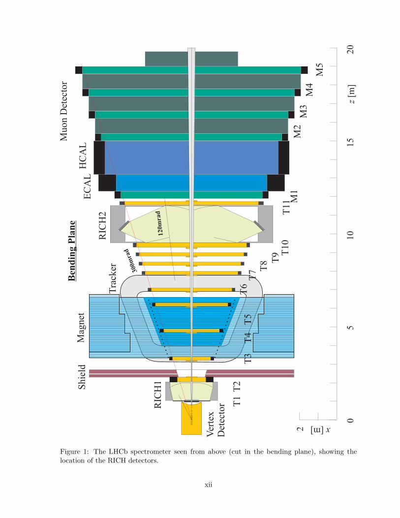
Figure 1: The LHCb spectrometer seen from above (cut in the bending plane), showing thelocation of the RICH detectors.
xii
1 Introduction
Particle identification is a fundamental re-quirement of the LHCb experiment. The abil-ity to distinguish between pions and kaons ina variety of final states is essential for thephysics that the experiment is designed tostudy: meaningful CP-violation measurementsare only possible in many important channelsif hadron identification is available.
The particle identification is achieved us-ing ring-imaging Cherenkov (RICH) detectors.Their placement within the LHCb spectrome-ter can be seen in Fig. 1, which shows the topview of the experiment. Details of the rest ofthe experiment can be found in [1, 2, 3].
In this introduction, the physics require-ments are discussed, and an overview is givenof the RICH detector system. A brief discus-sion of the evolution since the Technical Pro-posal is then given, before an outline of therest of the document.
0
1000
2000
3000
4000
5000
6000
7000
5 5.1 5.2 5.3 5.4 5.5
Invariant mass [GeV/c ] 2
Eve
nts
/ 2
0 M
eV/c
2
Without RICHBd → ππBd
b
→ πK
Bs → π
π
K
Bs
→→
KK
pKΛ
b→ pΛ
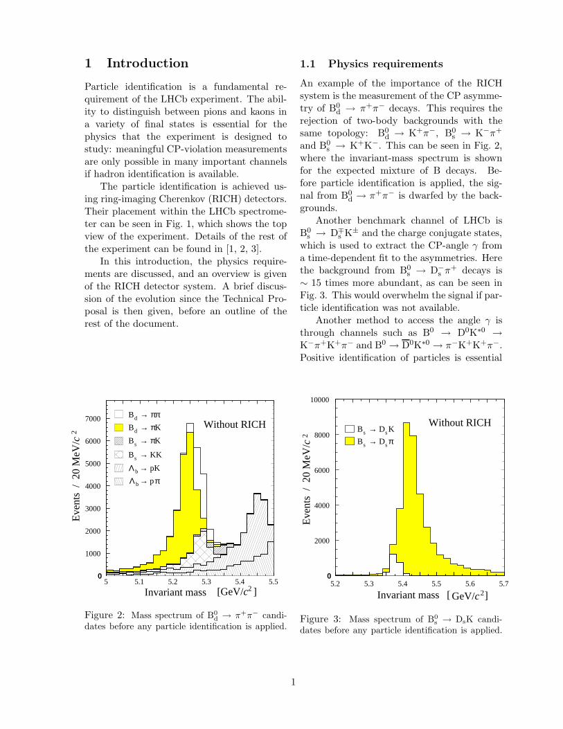
Figure 2: Mass spectrum of B0d → π+π− candi-
dates before any particle identification is applied.
1.1 Physics requirements
An example of the importance of the RICHsystem is the measurement of the CP asymme-try of B0
d → π+π− decays. This requires therejection of two-body backgrounds with thesame topology: B0
d → K+π−, B0s → K−π+
and B0s → K+K−. This can be seen in Fig. 2,
where the invariant-mass spectrum is shownfor the expected mixture of B decays. Be-fore particle identification is applied, the sig-nal from B0
d → π+π− is dwarfed by the back-grounds.
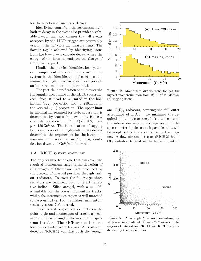
Another benchmark channel of LHCb isB0
s → D∓s K± and the charge conjugate states,
which is used to extract the CP-angle γ froma time-dependent fit to the asymmetries. Herethe background from B0
s → D−s π+ decays is
∼ 15 times more abundant, as can be seen inFig. 3. This would overwhelm the signal if par-ticle identification was not available.
Another method to access the angle γ isthrough channels such as B0 → D0K∗0 →K−π+K+π− and B0 → D0K∗0 → π−K+K+π−.Positive identification of particles is essential
0
2000
4000
6000
8000
10000
5.2 5.3 5.4 5.5 5.6 5.7
Invariant mass [ GeV/c2]
Eve
nts
/ 2
0 M
eV/c2
Without RICHBs → DsK
Bs → Dsπ
Figure 3: Mass spectrum of B0s → DsK candi-
dates before any particle identification is applied.
1
for the selection of such rare decays.Identifying kaons from the accompanying b
hadron decay in the event also provides a valu-able flavour tag, and ensures that all eventsaccepted by the LHCb trigger are potentiallyuseful in the CP violation measurements. Theflavour tag is achieved by identifying kaonsfrom the b → c → s cascade decay, where thecharge of the kaon depends on the charge ofthe initial b quark.
Finally, the particle-identification systemcan complement the calorimeters and muonsystem in the identification of electrons andmuons. For high mass particles it can providean improved momentum determination.
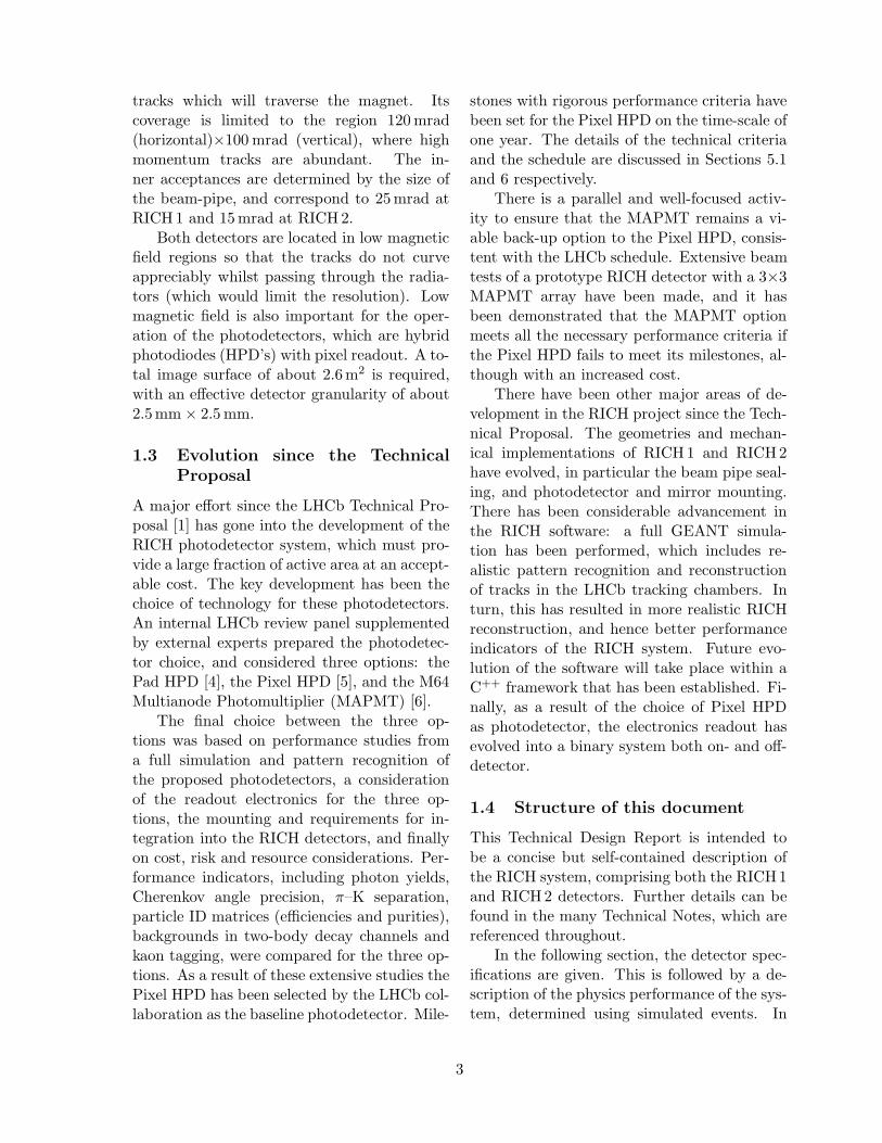
The particle identification should cover thefull angular acceptance of the LHCb spectrom-eter, from 10 mrad to 300 mrad in the hor-izontal (x, z) projection and to 250 mrad inthe vertical (y, z) projection. The upper limitin momentum required for π–K separation isdetermined by tracks from two-body B-decaychannels, as shown in Fig. 4 (a); 90% havep < 150GeV/c. The identification of taggingkaons and tracks from high multiplicity decaysdetermines the requirement for the lower mo-mentum limit. As shown in Fig. 4 (b), identi-fication down to 1GeV/c is desirable.
1.2 RICH system overview
The only feasible technique that can cover therequired momentum range is the detection ofring images of Cherenkov light produced bythe passage of charged particles through vari-ous radiators. To cover the full range, threeradiators are required, with different refrac-tive indices. Silica aerogel, with n = 1.03,is suitable for the lowest momentum tracks,whilst the intermediate region is well matchedto gaseous C4F10. For the highest momentumtracks, gaseous CF4 is used.
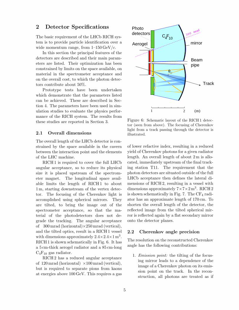
There is a strong correlation between thepolar angle and momentum of tracks, as seenin Fig. 5: at wide angles, the momentum spec-trum is softer. The RICH system is there-fore divided into two detectors. An upstreamdetector (RICH1) contains both the aerogel
0
200
100
300 (a)
0
20
40
60
80
0 5 10 15 20
(b)
Momentum (GeV/c)
Num
ber
of tr
acks
tagging kaons
B decay ππ
0 50 100 150 200
Figure 4: Momentum distributions for (a) thehighest momentum pion from B0
d → π+π− decays,(b) tagging kaons.
and C4F10 radiators, covering the full outeracceptance of LHCb. To minimize the re-quired photodetector area it is sited close tothe interaction region, and upstream of thespectrometer dipole to catch particles that willbe swept out of the acceptance by the mag-net. A downstream detector (RICH2) has aCF4 radiator, to analyse the high-momentum
0
100
200
300
400
0 50 100 150 200
Momentum[GeV/c]
θ [m
rad]
RICH-1
RICH-2
Figure 5: Polar angle θ versus momentum, forall tracks in simulated B0
d → π+π− events. Theregions of interest for RICH1 and RICH2 are in-dicated by the dashed lines.
2
tracks which will traverse the magnet. Itscoverage is limited to the region 120 mrad(horizontal)×100 mrad (vertical), where highmomentum tracks are abundant. The in-ner acceptances are determined by the size ofthe beam-pipe, and correspond to 25 mrad atRICH1 and 15 mrad at RICH2.
Both detectors are located in low magneticfield regions so that the tracks do not curveappreciably whilst passing through the radia-tors (which would limit the resolution). Lowmagnetic field is also important for the oper-ation of the photodetectors, which are hybridphotodiodes (HPD’s) with pixel readout. A to-tal image surface of about 2.6m2 is required,with an effective detector granularity of about2.5mm × 2.5 mm.
1.3 Evolution since the TechnicalProposal
A major effort since the LHCb Technical Pro-posal [1] has gone into the development of theRICH photodetector system, which must pro-vide a large fraction of active area at an accept-able cost. The key development has been thechoice of technology for these photodetectors.An internal LHCb review panel supplementedby external experts prepared the photodetec-tor choice, and considered three options: thePad HPD [4], the Pixel HPD [5], and the M64Multianode Photomultiplier (MAPMT) [6].
The final choice between the three op-tions was based on performance studies froma full simulation and pattern recognition ofthe proposed photodetectors, a considerationof the readout electronics for the three op-tions, the mounting and requirements for in-tegration into the RICH detectors, and finallyon cost, risk and resource considerations. Per-formance indicators, including photon yields,Cherenkov angle precision, π–K separation,particle ID matrices (efficiencies and purities),backgrounds in two-body decay channels andkaon tagging, were compared for the three op-tions. As a result of these extensive studies thePixel HPD has been selected by the LHCb col-laboration as the baseline photodetector. Mile-
stones with rigorous performance criteria havebeen set for the Pixel HPD on the time-scale ofone year. The details of the technical criteriaand the schedule are discussed in Sections 5.1and 6 respectively.
There is a parallel and well-focused activ-ity to ensure that the MAPMT remains a vi-able back-up option to the Pixel HPD, consis-tent with the LHCb schedule. Extensive beamtests of a prototype RICH detector with a 3×3MAPMT array have been made, and it hasbeen demonstrated that the MAPMT optionmeets all the necessary performance criteria ifthe Pixel HPD fails to meet its milestones, al-though with an increased cost.
There have been other major areas of de-velopment in the RICH project since the Tech-nical Proposal. The geometries and mechan-ical implementations of RICH1 and RICH2have evolved, in particular the beam pipe seal-ing, and photodetector and mirror mounting.There has been considerable advancement inthe RICH software: a full GEANT simula-tion has been performed, which includes re-alistic pattern recognition and reconstructionof tracks in the LHCb tracking chambers. Inturn, this has resulted in more realistic RICHreconstruction, and hence better performanceindicators of the RICH system. Future evo-lution of the software will take place within aC++ framework that has been established. Fi-nally, as a result of the choice of Pixel HPDas photodetector, the electronics readout hasevolved into a binary system both on- and off-detector.
1.4 Structure of this document
This Technical Design Report is intended tobe a concise but self-contained description ofthe RICH system, comprising both the RICH1and RICH2 detectors. Further details can befound in the many Technical Notes, which arereferenced throughout.
In the following section, the detector spec-ifications are given. This is followed by a de-scription of the physics performance of the sys-tem, determined using simulated events. In
3

Section 4 an overview is given of the resultsobtained in the laboratory and test-beam us-ing prototypes, which give confidence that theexpected performance will be achieved. Thetechnical design of the detectors is presented inSection 5. The issues of project organisation,including the schedule and cost, are discussedin Section 6, and finally details are given forthe back-up photodetector in Appendix A.
4
2 Detector Specifications
The basic requirement of the LHCb RICH sys-tem is to provide particle identification over awide momentum range, from 1–150 GeV/c.
In this section the principal features of thedetectors are described and their main param-eters are listed. Their optimization has beenconstrained by limits on the space available, onmaterial in the spectrometer acceptance andon the overall cost, to which the photon detec-tors contribute about 50%.
Prototype tests have been undertakenwhich demonstrate that the parameters listedcan be achieved. These are described in Sec-tion 4. The parameters have been used in sim-ulation studies to evaluate the physics perfor-mance of the RICH system. The results fromthese studies are reported in Section 3.
2.1 Overall dimensions
The overall length of the LHCb detector is con-strained by the space available in the cavernbetween the interaction point and the elementsof the LHC machine.
RICH1 is required to cover the full LHCbangular acceptance, so to reduce its physicalsize it is placed upstream of the spectrom-eter magnet. The longitudinal space avail-able limits the length of RICH1 to about1m, starting downstream of the vertex detec-tor. The focusing of the Cherenkov light isaccomplished using spherical mirrors. Theyare tilted, to bring the image out of thespectrometer acceptance, so that the ma-terial of the photodetectors does not de-grade the tracking. The angular acceptanceof 300mrad (horizontal)×250mrad (vertical),and the tilted optics, result in a RICH1 vesselwith dimensions approximately 2.4×2.4×1m3.RICH1 is shown schematically in Fig. 6. It hasa 5 cm-thick aerogel radiator and a 85 cm-longC4F10 gas radiator.
RICH2 has a reduced angular acceptanceof 120mrad (horizontal) ×100mrad (vertical),but is required to separate pions from kaonsat energies above 100GeV. This requires a gas
1 2 (m)
θC
mirrorAerogel
Beampipe
Track
Photodetectors 300 mrad
C F 4 10
Figure 6: Schematic layout of the RICH 1 detec-tor (seen from above). The focusing of Cherenkovlight from a track passing through the detector isillustrated.
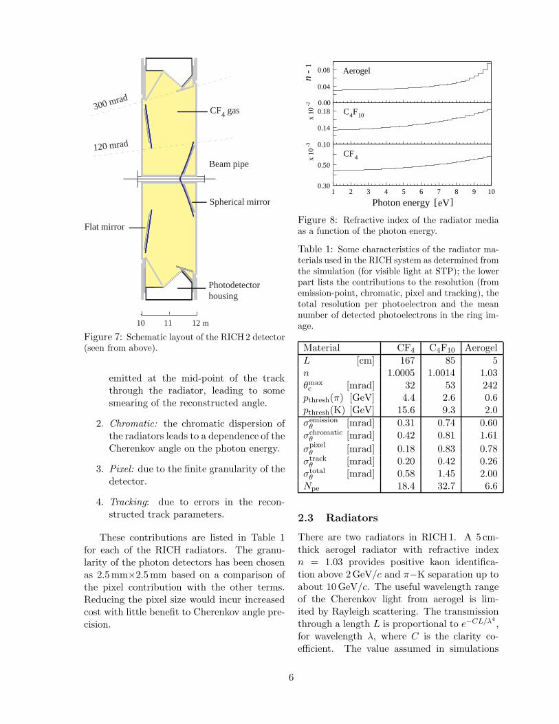
of lower refactive index, resulting in a reducedyield of Cherenkov photons for a given radiatorlength. An overall length of about 2m is allo-cated, immediately upstream of the final track-ing station T11. The requirement that thephoton detectors are situated outside of the fullLHCb acceptance then defines the lateral di-mensions of RICH2, resulting in a vessel withdimensions approximately 7×7×2m3. RICH2is shown schematically in Fig. 7. The CF4 radi-ator has an approximate length of 170 cm. Toshorten the overall length of the detector, thereflected image from the tilted spherical mir-ror is reflected again by a flat secondary mirroronto the detector planes.
2.2 Cherenkov angle precision
The resolution on the reconstructed Cherenkovangle has the following contributions:
1. Emission point: the tilting of the focus-ing mirror leads to a dependence of theimage of a Cherenkov photon on its emis-sion point on the track. In the recon-struction, all photons are treated as if
5
CF4 gas
Beam pipe
300 mrad
120 mrad
Flat mirror
Spherical mirror
Photodetectorhousing
10 11 12 m
Figure 7: Schematic layout of the RICH2 detector(seen from above).
emitted at the mid-point of the trackthrough the radiator, leading to somesmearing of the reconstructed angle.
2. Chromatic: the chromatic dispersion ofthe radiators leads to a dependence of theCherenkov angle on the photon energy.
3. Pixel: due to the finite granularity of thedetector.
4. Tracking: due to errors in the recon-structed track parameters.
These contributions are listed in Table 1for each of the RICH radiators. The granu-larity of the photon detectors has been chosenas 2.5mm×2.5mm based on a comparison ofthe pixel contribution with the other terms.Reducing the pixel size would incur increasedcost with little benefit to Cherenkov angle pre-cision.
0.04
0.08
n - 1 Aerogel
0.10
0.14
0.18 C4F10x 10
-2
0.30
0.50
1 2 3 4 5 6 7 8 9 10
CF4x 10
-3
Photon energy [ eV ]
0.00
Figure 8: Refractive index of the radiator mediaas a function of the photon energy.
Table 1: Some characteristics of the radiator ma-terials used in the RICH system as determined fromthe simulation (for visible light at STP); the lowerpart lists the contributions to the resolution (fromemission-point, chromatic, pixel and tracking), thetotal resolution per photoelectron and the meannumber of detected photoelectrons in the ring im-age.
Material CF4 C4F10 AerogelL [cm] 167 85 5n 1.0005 1.0014 1.03θmaxc [mrad] 32 53 242
pthresh(π) [GeV] 4.4 2.6 0.6pthresh(K) [GeV] 15.6 9.3 2.0σemission
θ [mrad] 0.31 0.74 0.60σchromatic
θ [mrad] 0.42 0.81 1.61σpixel
θ [mrad] 0.18 0.83 0.78σtrack
θ [mrad] 0.20 0.42 0.26σtotal
θ [mrad] 0.58 1.45 2.00Npe 18.4 32.7 6.6
2.3 Radiators
There are two radiators in RICH1. A 5 cm-thick aerogel radiator with refractive indexn = 1.03 provides positive kaon identifica-tion above 2 GeV/c and π−K separation up toabout 10 GeV/c. The useful wavelength rangeof the Cherenkov light from aerogel is lim-ited by Rayleigh scattering. The transmissionthrough a length L is proportional to e−CL/λ4
,for wavelength λ, where C is the clarity co-efficient. The value assumed in simulations
6
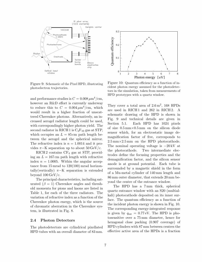
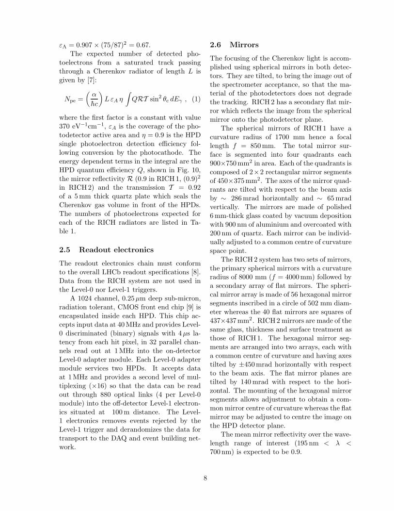
Figure 9: Schematic of the Pixel HPD, illustratingphotoelectron trajectories.
and performance studies is C = 0.008µm4/cm,however an R&D effort is currently underwayto reduce this to C = 0.004µm4/cm, whichwould result in a higher fraction of unscat-tered Cherenkov photons. Alternatively, an in-creased aerogel radiator length could be used,with correspondingly higher photon yield. Thesecond radiator in RICH1 is C4F10 gas at STP,which occupies an L = 85 cm path length be-tween the aerogel and the spherical mirror.The refractive index is n = 1.0014 and it pro-vides π−K separation up to about 50 GeV/c.
RICH2 contains CF4 gas at STP, provid-ing an L = 167 cm path length with refractiveindex n = 1.0005. Within the angular accep-tance from 15 mrad to 120(100) mrad horizon-tally(vertically) π−K separation is extendedbeyond 100 GeV/c.
The principal characteristics, including sat-urated (β = 1) Cherenkov angles and thresh-old momenta for pions and kaons are listed inTable 1, for each of the three radiators. Thevariation of refractive index as a function of theCherenkov photon energy, which is the sourceof chromatic aberration in the Cherenkov sys-tem, is illustrated in Fig. 8.
2.4 Photon Detectors
The photodetectors are cylindrical pixellatedHPD tubes with an overall diameter of 83 mm.
0
0.1
0.2
0.3
1 2 3 4 5 6 7 8
Photon energy [ eV ]
Qua
ntum
effi
cien
cy
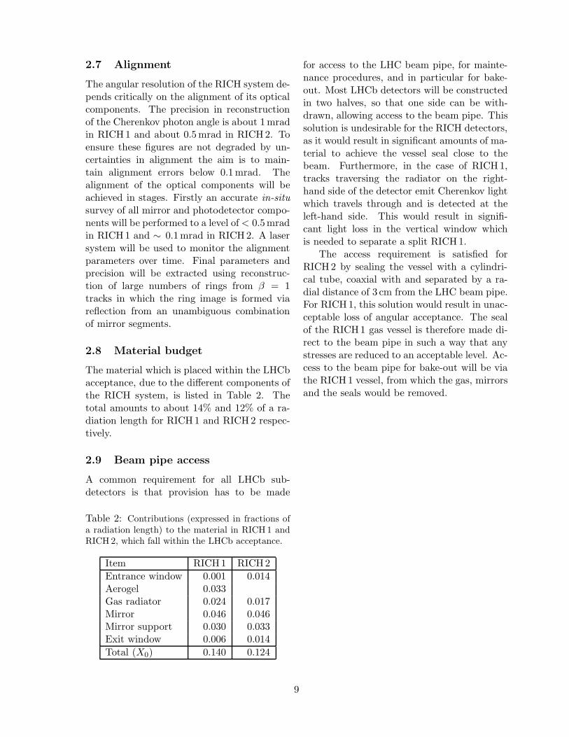
Figure 10: Quantum efficiency as a function of in-cident photon energy assumed for the photodetec-tors in the simulation, taken from measurements ofHPD prototypes with a quartz window.
They cover a total area of 2.6 m2, 168 HPDsare used in RICH1 and 262 in RICH2. Aschematic drawing of the HPD is shown inFig. 9 and technical details are given inSection 5.1. Each HPD has 1024 pixelsof size 0.5mm×0.5mm on the silicon diodesensor which, for an electrostatic image de-magnification factor of five, corresponds to2.5 mm×2.5mm on the HPD photocathode.The nominal operating voltage is −20 kV atthe photocathode. Two intermediate elec-trodes define the focusing properties and thedemagnification factor, and the silicon sensoranode is at ground potential. Each tube issurrounded by a magnetic shield in the formof a Mu-metal cylinder of 140 mm length and86 mm outer diameter, that extends 20 mm be-yond the centre of the entrance window.
The HPD has a 7 mm thick, sphericalquartz entrance window with an S20 (multial-kali) photocathode deposited on its inner sur-face. The quantum efficiency as a function ofthe incident photon energy is shown in Fig. 10.The corresponding energy-integrated responseis given by qint = 0.77 eV. The HPD is pho-tosensitive over a 75 mm diameter, hence forhexagonal close packing (0.907 coverage) ofHPD cylinders with 87 mm between centres theeffective active area of the HPDs is a fraction
7
εA = 0.907 × (75/87)2 = 0.67.The expected number of detected pho-
toelectrons from a saturated track passingthrough a Cherenkov radiator of length L isgiven by [7]:
Npe =(
α
hc
)LεA η
∫QRT sin2 θc dEγ , (1)
where the first factor is a constant with value370 eV−1cm−1, εA is the coverage of the pho-todetector active area and η = 0.9 is the HPDsingle photoelectron detection efficiency fol-lowing conversion by the photocathode. Theenergy dependent terms in the integral are theHPD quantum efficiency Q, shown in Fig. 10,the mirror reflectivity R (0.9 in RICH1, (0.9)2
in RICH2) and the transmission T = 0.92of a 5 mm thick quartz plate which seals theCherenkov gas volume in front of the HPDs.The numbers of photoelectrons expected foreach of the RICH radiators are listed in Ta-ble 1.
2.5 Readout electronics
The readout electronics chain must conformto the overall LHCb readout specifications [8].Data from the RICH system are not used inthe Level-0 nor Level-1 triggers.
A 1024 channel, 0.25µm deep sub-micron,radiation tolerant, CMOS front end chip [9] isencapsulated inside each HPD. This chip ac-cepts input data at 40 MHz and provides Level-0 discriminated (binary) signals with 4µs la-tency from each hit pixel, in 32 parallel chan-nels read out at 1MHz into the on-detectorLevel-0 adapter module. Each Level-0 adaptermodule services two HPDs. It accepts dataat 1MHz and provides a second level of mul-tiplexing (×16) so that the data can be readout through 880 optical links (4 per Level-0module) into the off-detector Level-1 electron-ics situated at 100 m distance. The Level-1 electronics removes events rejected by theLevel-1 trigger and derandomizes the data fortransport to the DAQ and event building net-work.
2.6 Mirrors
The focusing of the Cherenkov light is accom-plished using spherical mirrors in both detec-tors. They are tilted, to bring the image out ofthe spectrometer acceptance, so that the ma-terial of the photodetectors does not degradethe tracking. RICH2 has a secondary flat mir-ror which reflects the image from the sphericalmirror onto the photodetector plane.
The spherical mirrors of RICH1 have acurvature radius of 1700 mm hence a focallength f = 850mm. The total mirror sur-face is segmented into four quadrants each900×750mm2 in area. Each of the quadrants iscomposed of 2×2 rectangular mirror segmentsof 450×375mm2. The axes of the mirror quad-rants are tilted with respect to the beam axisby ∼ 286 mrad horizontally and ∼ 65 mradvertically. The mirrors are made of polished6 mm-thick glass coated by vacuum depositionwith 900 nm of aluminium and overcoated with200 nm of quartz. Each mirror can be individ-ually adjusted to a common centre of curvaturespace point.
The RICH2 system has two sets of mirrors,the primary spherical mirrors with a curvatureradius of 8000 mm (f = 4000mm) followed bya secondary array of flat mirrors. The spheri-cal mirror array is made of 56 hexagonal mirrorsegments inscribed in a circle of 502 mm diam-eter whereas the 40 flat mirrors are squares of437×437mm2. RICH2 mirrors are made of thesame glass, thickness and surface treatment asthose of RICH1. The hexagonal mirror seg-ments are arranged into two arrays, each witha common centre of curvature and having axestilted by ±450mrad horizontally with respectto the beam axis. The flat mirror planes aretilted by 140 mrad with respect to the hori-zontal. The mounting of the hexagonal mirrorsegments allows adjustment to obtain a com-mon mirror centre of curvature whereas the flatmirror may be adjusted to centre the image onthe HPD detector plane.
The mean mirror reflectivity over the wave-length range of interest (195 nm < λ <700 nm) is expected to be 0.9.
8
2.7 Alignment
The angular resolution of the RICH system de-pends critically on the alignment of its opticalcomponents. The precision in reconstructionof the Cherenkov photon angle is about 1 mradin RICH1 and about 0.5 mrad in RICH2. Toensure these figures are not degraded by un-certainties in alignment the aim is to main-tain alignment errors below 0.1 mrad. Thealignment of the optical components will beachieved in stages. Firstly an accurate in-situsurvey of all mirror and photodetector compo-nents will be performed to a level of < 0.5mradin RICH1 and ∼ 0.1mrad in RICH2. A lasersystem will be used to monitor the alignmentparameters over time. Final parameters andprecision will be extracted using reconstruc-tion of large numbers of rings from β = 1tracks in which the ring image is formed viareflection from an unambiguous combinationof mirror segments.
2.8 Material budget
The material which is placed within the LHCbacceptance, due to the different components ofthe RICH system, is listed in Table 2. Thetotal amounts to about 14% and 12% of a ra-diation length for RICH1 and RICH2 respec-tively.
2.9 Beam pipe access
A common requirement for all LHCb sub-detectors is that provision has to be made
Table 2: Contributions (expressed in fractions ofa radiation length) to the material in RICH1 andRICH 2, which fall within the LHCb acceptance.
Item RICH1 RICH2Entrance window 0.001 0.014Aerogel 0.033Gas radiator 0.024 0.017Mirror 0.046 0.046Mirror support 0.030 0.033Exit window 0.006 0.014Total (X0) 0.140 0.124
for access to the LHC beam pipe, for mainte-nance procedures, and in particular for bake-out. Most LHCb detectors will be constructedin two halves, so that one side can be with-drawn, allowing access to the beam pipe. Thissolution is undesirable for the RICH detectors,as it would result in significant amounts of ma-terial to achieve the vessel seal close to thebeam. Furthermore, in the case of RICH1,tracks traversing the radiator on the right-hand side of the detector emit Cherenkov lightwhich travels through and is detected at theleft-hand side. This would result in signifi-cant light loss in the vertical window whichis needed to separate a split RICH1.
The access requirement is satisfied forRICH2 by sealing the vessel with a cylindri-cal tube, coaxial with and separated by a ra-dial distance of 3 cm from the LHC beam pipe.For RICH1, this solution would result in unac-ceptable loss of angular acceptance. The sealof the RICH1 gas vessel is therefore made di-rect to the beam pipe in such a way that anystresses are reduced to an acceptable level. Ac-cess to the beam pipe for bake-out will be viathe RICH1 vessel, from which the gas, mirrorsand the seals would be removed.
9
3 Physics Performance
The performance of the RICH system has beenstudied using simulated data. In this sectionthe inputs to the simulation are described, anddetails are given concerning the reconstruc-tion and pattern-recognition algorithms. TheRICH performance is characterized, and theparticle identification results are shown in var-ious physics channels of interest. Further de-tails can be found in [10].
3.1 Description of simulation
Proton-proton interactions at√
s = 14 TeV aresimulated using the PYTHIA event generator,version 6.1 [11]. The parton distributions aretaken from CTEQ4L. A multiple-interactionmodel is used, with varying impact parameterand running pT cut-off, tuned to reproduce ex-isting low-energy data [12]. A GEANT3-basedprogram simulates the effect of the LHCb ap-paratus, and is used to reconstruct the events.It includes all secondary interaction processes,with thresholds of 1 MeV for electrons/photonsand 10 MeV for hadrons. The results presentedhere are based on a sample of 150 000 eventsof signal and background decays.
The description of the RICH detectors fol-lows as closely as possible the designs given inthis report, including radiator volumes, mir-rors, vessel walls and photodetector planes.Events were generated and the input and exitpoints of all charged particles traversing theradiators were recorded. Information was alsorecorded for any particle striking the photode-tector plane.
The simulation of the Cherenkov processis then performed with custom-written LHCbcode after the GEANT step. This enabledstudies to be conveniently made with differ-ent sets of parameters. Taking the input andexit point of the traversing particle in each ra-diator, the path length is determined, and thecorresponding number of Cherenkov photonscalculated from Eq. 1.
The Cherenkov generation is performedover the photon energy intervals 1.75 < Eγ <
7 eV for the gases, and 1.75 < Eγ < 3.5 eVfor aerogel, for which a plastic window cutsoff the high energies. The variation of refrac-tive index with photon energy is parametrizedusing the Sellmeir coefficient formalism, as in-dicated in Fig. 8. Photons are generated withthis chromatic dependence and their emissionpoint distributed uniformly along the particletrajectory. Each photon is traced through thecounter until it reaches the detector plane, orleaves the acceptance. The following sourcesof photon loss are considered:
1. Mirror reflectivity: 90% is assumed, in-dependent of wavelength in the region ofinterest, following measurements made ofprototype mirrors;
2. Quartz window: foreseen to isolate thephotodetectors from the radiator gas, an8% loss is included;
3. Rayleigh scattering: in the aerogel, wherea clarity coefficient of C = 0.008µm4/cmis assumed (see Section 2.3);
4. Detection efficiency: of photoelectrons inthe HPD, discussed below, 90% is as-sumed.
The photocathode efficiency is included in thecounter simulation at the earliest level of gen-eration, to save computer time.
3.1.1 Photodetector simulation
The photons incident on the photodetectorplane are input to an HPD simulation. Withinthis simulation the HPDs are tiled on the pho-todetector plane as specified in the engineer-ing design studies, forming a hexagonal close-packed arrangement with 87mm between tubecentres along the local vertical axis, and stag-gered in the orthogonal coordinate. The shad-owing effect of the Mu-metal shields is not im-plemented, but will be minimized by the fore-seen “pointing” layout of the HPDs. A diam-eter of 75mm around each tube centre is con-sidered to be sensitive.
10
The electron optics of the tubes is not mod-elled in detail. A simple Gaussian smearing of230µm is applied to each impact point prior topixellisation, to account for the point spreadfunction in the optics, mapped back to thephotocathode window. An effective squarepixel size of 2.4 mm is assumed at the window.
A photoelectron striking a pixel has thepossibility to deposit only a fraction of its en-ergy, and then to backscatter. This is mod-elled and convoluted with a detector responseto give a pulse height in the struck pixel.Each pixel may receive hits from more thanone photoelectron. A threshold is applied,above which all signal is counted as a sin-gle hit in order to simulate the binary elec-tronics. The parameters are adjusted to givethe expected single photoelectron detection ef-ficiency of 90%. The simulation supports thepossibility of tracking the backscattered photo-electrons onto other pixels, however the proba-bility of secondary hits is found to be negligiblecompared to backgrounds from genuine tracks.
Information is retained within the simula-tion on the incident particles and radiator pro-cess which gave rise to each hit pixel. Thisinformation has been exploited to study, forinstance, the Cherenkov angle resolutions andthe contribution of secondary tracks.
3.1.2 Simulated backgrounds
The RICH detector simulation produces radia-tion not only from those primary tracks whichpass through the whole radiator length, butfrom all background sources which appear inthe GEANT simulation. These include:
1. Traversing particles: HPDs may reactnot only to incident photons, but alsoto charged particles passing through thedetector, radiating Cherenkov light inthe tube window. Within the simulationthese particles may arise in both RICH1and RICH2 from wide-angle tracks, andin RICH1 alone from soft tracks bentbackwards in the magnetic field. Theincident positions of these tracks arerecorded and the HPD response then
simulated with a set of parameterizeddistributions which vary as a functionof incident angle. The parameterizationwas calibrated by comparing data takenin test beams with photodetectors ex-posed to charged particles, against de-tailed stand-alone simulations of singletubes.
2. Scattered photons: The Rayleigh-scattered photons from the aerogel,discussed above, provide a diffusebackground in RICH1.
3. Backward-going tracks: Secondarieswhich emerge from the beam-pipe orother material into the radiator aresimulated, and these include tracksthat travel backwards (particularly inRICH1), which may radiate directly intothe photodetectors, giving clusters of hitsunfocused by the mirror.
4. Unreconstructed tracks: All particlestraversing the RICH radiators, thatare above threshold, produce Cherenkovlight in the simulation. Some of these,due to their wide angle or low momen-tum, will not be reconstructed by thetracking system, and therefore providebackground hits for the pattern recogni-tion.
5. Electronic and detector noise: The ef-fect of random noise in the detectors hasbeen studied, and is found to be smalluntil the probability of a pixel firing isincreased beyond 1%, much greater thanthe predicted level of gaussian noise inthe front-end electronics. This followsbecause the ring-images are searched forusing the predictions from the trackingsystem, and the likelihoods of differentparticle-type hypotheses are then com-pared; this comparison is robust againstadditional random hits.
11
3.1.3 Tracking
Tracking information is essential for the recon-struction of RICH events. Tracker hits aresimulated with a resolution of ∼ 200µm forthe outer tracker, and 100µm for the innertracker. Tracks are reconstructed by fittingthese, and any Vertex Detector space points,using a Kalman filter method. At presentthere is no pattern recognition implementedfor the tracking, so Monte Carlo truth infor-mation is used to feed the fit with the cor-rect string of hits. Tracks are defined whichare suitable for the physics analysis, by requir-ing that the particle passed through the mag-net, that it is above 1GeV, and that it hasa minimum number of tracker space points.The RICH performance is evaluated on thesewell-reconstructed tracks, of which there aretypically 30 which pass through the detectorsin triggered signal events. The momentumresolution of these tracks is 0.35% for non-electrons. Tracks of lower quality, includingthose with unreliable or non-existent momen-tum information, are also fitted. These areused in the RICH pattern recognition to iden-tify background rings caused by low momen-tum and wide angle tracks resulting from sec-ondary interactions.
3.2 Pattern recognition
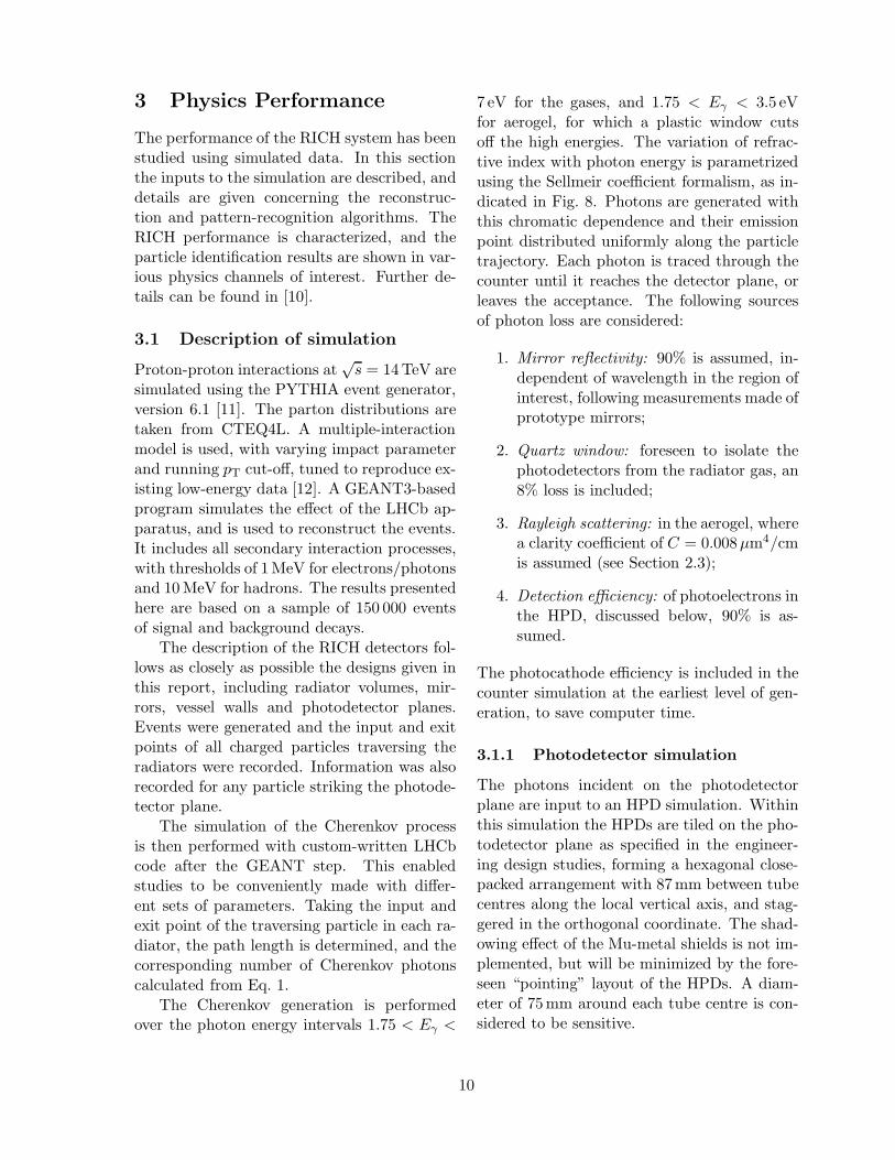
A simulated bb event in the two RICH detec-tors is shown in Fig. 11 and 12. The two de-tector planes of each RICH are drawn side byside, dots mark the positions of detected pho-toelectrons, and the expected ring images aresuperimposed.
The Cherenkov rings are not perfect cir-cles, but are roughly elliptical in shape, witha degree of distortion that depends on the di-rection of the track within the acceptance. In-stead of attempting to directly fit these rings,a substantial simplification is achieved by re-constructing the Cherenkov angles at emission(θc, φc) for each hit under the assumption thatit originated from a given track [7]. Thatcalculation accounts for the mirror geometry,and involves the solution of a quartic equa-
tion [13]. The hits which truly originate fromthat track will then all have the same valueof polar Cherenkov angle θc (within the res-olution), and have uniformly distributed az-imuthal angle φc.
The task of the pattern recognition is to as-sign a particle type to each track, so as to bestdescribe the observed hits. Two approacheshave been developed: a “local” method whichtreats each track separately (and is thereforefast), and a “global” method that optimisesthe assignment of particle types for all tracksin RICH1 and RICH2 in the event simultane-ously, to give the most accurate possible par-ticle identification. A third approach is alsounder study, searching for rings in the RICHdata, without relying on the information fromthe tracking detectors: this may be useful asa later stage in the reconstruction, to help inthe rejection of background hits after a firstpass has been made using the tracking infor-mation [14].
3.2.1 Local analysis
In the local method [15] each track is takenin turn, and the Cherenkov angle of each hitin the detector is calculated relative to thattrack. For each track a log-likelihood functionis calculated, proportional to:
∑i
ln
(1 +
1√2πσθκ
exp
[−(θi − θx)2
2σ2θ
]),
(2)where θi is the reconstructed emission angleof hit i, θx is the expected emission angle ofthe track under particle-type hypothesis x, andσθ is the angular resolution. κ is a hit se-lection parameter, which defines an effectivebandwidth around the considered Cherenkovangle θi; a value κ = 1 is found to give the bestperformance. The normalisation is chosen suchthat the value of the log-likelihood functioncorresponds to the number of hits expected atangle θ. The sum is performed over all hits,but excludes those with θi much greater thanthe saturated Cherenkov angle to save CPUtime.
12
Figure 11: Event display of a simulated B0d →
π+π− event, with the photodetector planes ofRICH 1 drawn side by side (scale in cm), and theCherenkov rings superimposed.
The log-likelihood function is used to cal-culate the number of hits which can be at-tributed to a given particle-type hypothesis,evaluated at the mean Cherenkov emission an-gle. A Poisson probability is then calculatedfrom the comparison of the number of recon-structed hits with the number expected, fromEq. (1), and this is used to discriminate be-tween the different particle hypotheses.
This algorithm is a factor of 5 faster thanthe standard (global) approach. The possibil-ity of using it in the trigger, at Level-3, is understudy.
3.2.2 Global analysis
Instead of treating each track separately, inthe global method [13] the likelihood is con-structed for the whole event. In this way themain “background” for a track in the localmethod, due to hits from other tracks, is cor-rectly accounted for. For a given choice of par-ticle type for each track, a likelihood is calcu-lated that all the hits observed were producedby the tracks reconstructed in the event, plusunseen secondaries, noise etc. The particle-type assumptions are then changed and thelikelihood recalculated; in this way the set ofparticle types that maximises the likelihood is
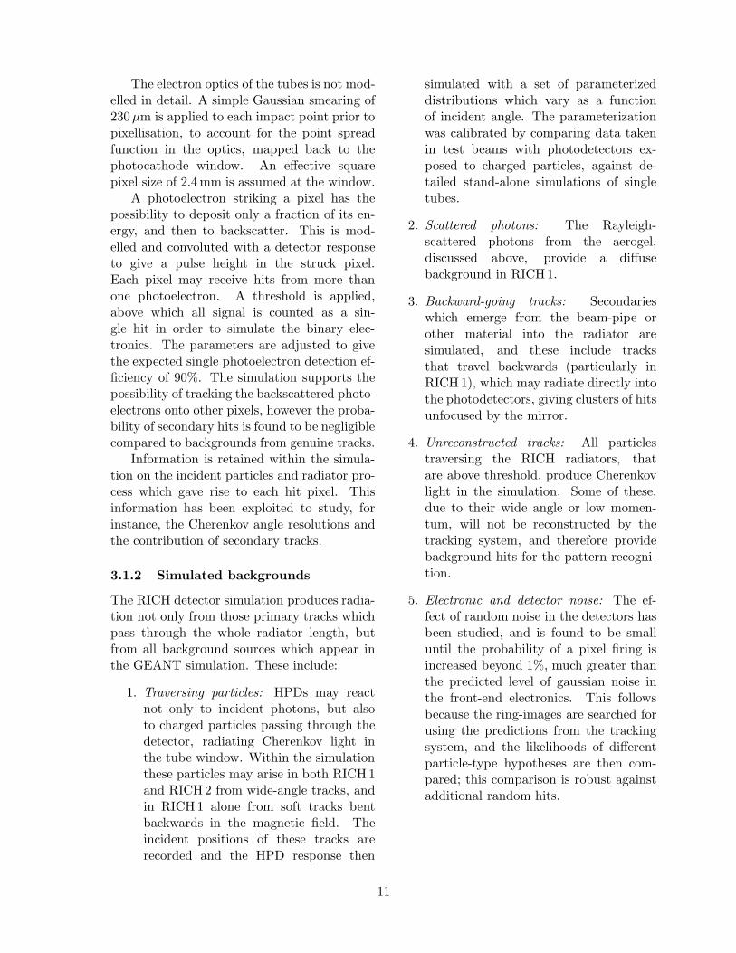
Figure 12: Event display of the same event asFig. 11, for RICH2.
searched for.The event likelihood is calculated by com-
paring the number of photoelectrons detectedin each pixel with the number expected in thatpixel from all sources: signal (the Cherenkovrings from the various radiators), and back-grounds (from scattering in the aerogel, ringswith no reconstructed tracks, electronic noise,etc.). A fitting function is calculated as theexpected number of photoelectrons detected ineach pixel, for a given choice of particle typesfor the tracks in the event. For the signal froma single track, that fitting function takes theform of a ring with roughly Gaussian cross-section in radius (the parametrization is Gaus-sian as a function of the Cherenkov emissionangle θc, and that is then converted to thedetector plane using the RICH optics). Thefitting function is illustrated in Fig. 13 for azoomed region of Fig. 11, for a given set oftrack hypotheses. The likelihood is then deter-mined from comparison of the fitting functionand the observed photoelectron signals. It hasthe form [13]:
lnL = −∑
track j
µj + (3)
∑pixel i
ni ln
∑
track j
aij + bi
,
where aij is the expected number of detected
13
-20-18
-16-14
-12-10
-8-6
-4-2
0
6
8
10
12
14
16
18
20
22
24
0
0.5
x (cm
)y (cm
)
Pro
b
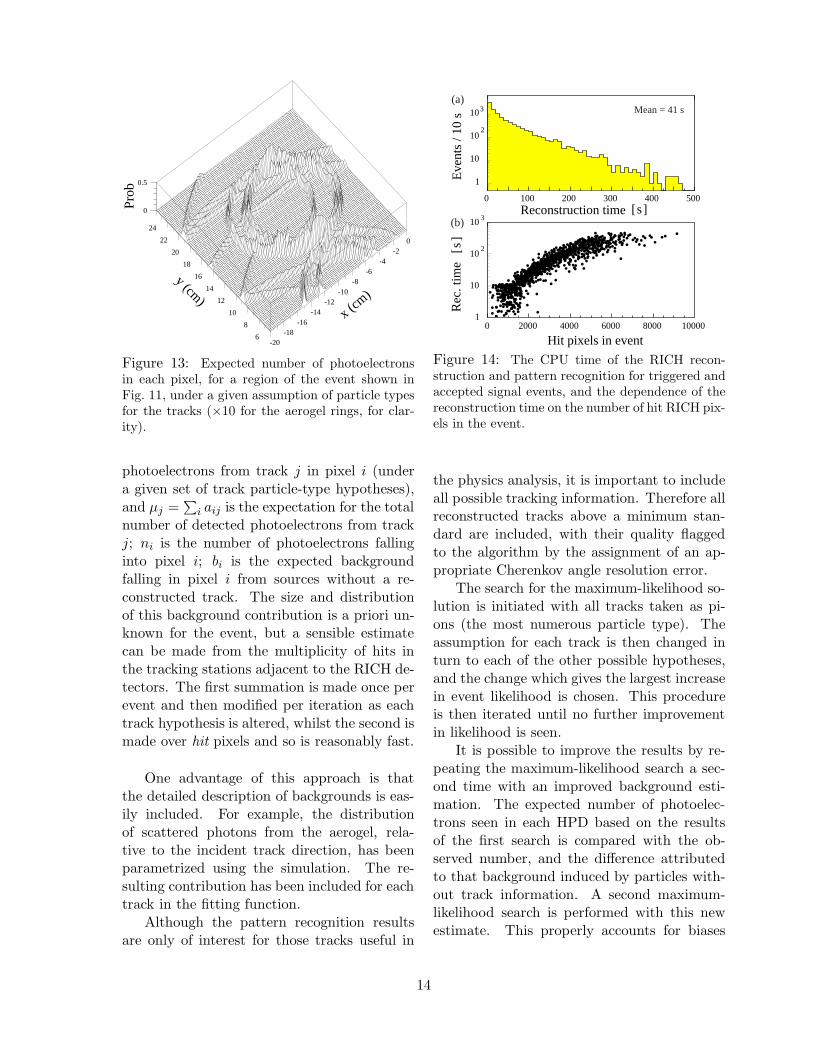
Figure 13: Expected number of photoelectronsin each pixel, for a region of the event shown inFig. 11, under a given assumption of particle typesfor the tracks (×10 for the aerogel rings, for clar-ity).
photoelectrons from track j in pixel i (undera given set of track particle-type hypotheses),and µj =
∑i aij is the expectation for the total
number of detected photoelectrons from trackj; ni is the number of photoelectrons fallinginto pixel i; bi is the expected backgroundfalling in pixel i from sources without a re-constructed track. The size and distributionof this background contribution is a priori un-known for the event, but a sensible estimatecan be made from the multiplicity of hits inthe tracking stations adjacent to the RICH de-tectors. The first summation is made once perevent and then modified per iteration as eachtrack hypothesis is altered, whilst the second ismade over hit pixels and so is reasonably fast.
One advantage of this approach is thatthe detailed description of backgrounds is eas-ily included. For example, the distributionof scattered photons from the aerogel, rela-tive to the incident track direction, has beenparametrized using the simulation. The re-sulting contribution has been included for eachtrack in the fitting function.
Although the pattern recognition resultsare only of interest for those tracks useful in
1
10
102
103
0 100 200 300 400 500Reconstruction time [ s ]
Eve
nts
/ 10
s
1
10
102
103
0 2000 4000 6000 8000 10000
Hit pixels in event
Rec
. tim
e [ s
]
Mean = 41 s(a)
(b)
Figure 14: The CPU time of the RICH recon-struction and pattern recognition for triggered andaccepted signal events, and the dependence of thereconstruction time on the number of hit RICH pix-els in the event.
the physics analysis, it is important to includeall possible tracking information. Therefore allreconstructed tracks above a minimum stan-dard are included, with their quality flaggedto the algorithm by the assignment of an ap-propriate Cherenkov angle resolution error.
The search for the maximum-likelihood so-lution is initiated with all tracks taken as pi-ons (the most numerous particle type). Theassumption for each track is then changed inturn to each of the other possible hypotheses,and the change which gives the largest increasein event likelihood is chosen. This procedureis then iterated until no further improvementin likelihood is seen.
It is possible to improve the results by re-peating the maximum-likelihood search a sec-ond time with an improved background esti-mation. The expected number of photoelec-trons seen in each HPD based on the resultsof the first search is compared with the ob-served number, and the difference attributedto that background induced by particles with-out track information. A second maximum-likelihood search is performed with this newestimate. This properly accounts for biases
14
RICH-1 PrimariesSecondaries
0
200
400
600
800
Hit pixels
Eve
nts
/ 100
hits
RICH-2
0
500
1000
1500
0 500 1000 1500 2000 2500 3000 3500
(a)
(b)0 1000 2000 3000 4000 5000 6000
Figure 15: Number of hit pixels per event in Level-0 triggered and accepted two-body events for (a)RICH 1, (b) RICH2.
caused by, for instance, local hot spots arisingfrom charged particles incident on HPD win-does.
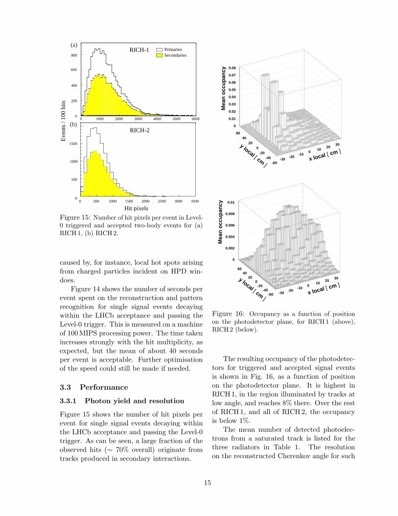
Figure 14 shows the number of seconds perevent spent on the reconstruction and patternrecognition for single signal events decayingwithin the LHCb acceptance and passing theLevel-0 trigger. This is measured on a machineof 100 MIPS processing power. The time takenincreases strongly with the hit multiplicity, asexpected, but the mean of about 40 secondsper event is acceptable. Further optimisationof the speed could still be made if needed.
3.3 Performance
3.3.1 Photon yield and resolution
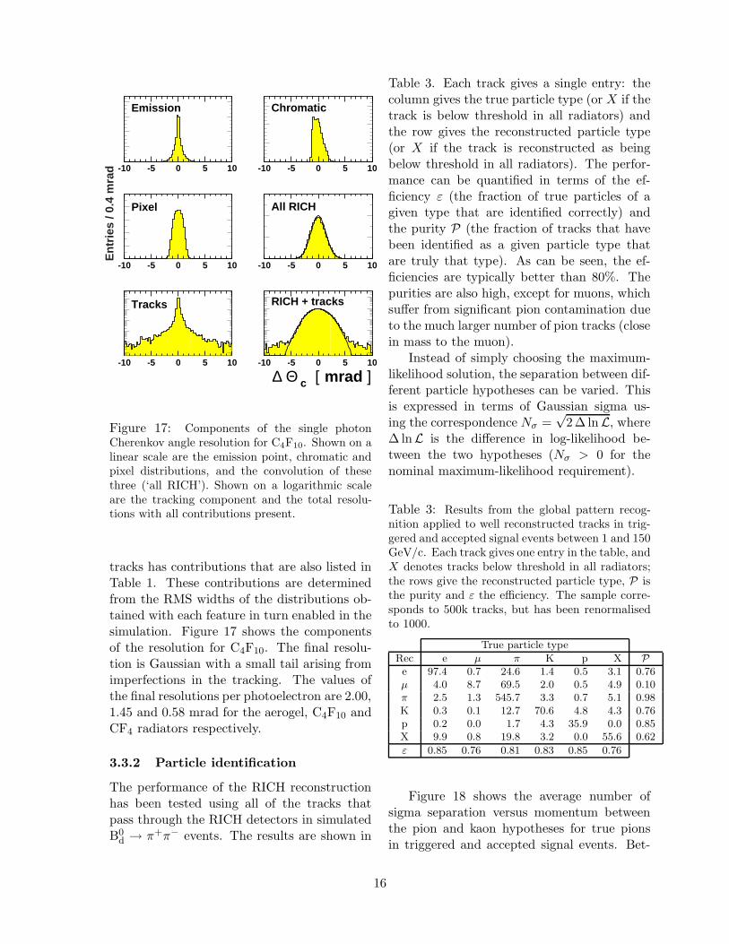
Figure 15 shows the number of hit pixels perevent for single signal events decaying withinthe LHCb acceptance and passing the Level-0trigger. As can be seen, a large fraction of theobserved hits (∼ 70% overall) originate fromtracks produced in secondary interactions.
-30-20
-100
1020
30
-60-40
-200
2040
60
0
0.01
0.02
0.03
0.04
0.05
0.06
0.07
0.08
x local [ cm ]y local [ cm ]
Mea
n oc
cupa
ncy
-30-20
-100
1020
30
-60-40
-200
2040
60
0
0.002
0.004
0.006
0.008
0.01
x local [ cm ]y local [ cm ]
Mea
n oc
cupa
ncy
Figure 16: Occupancy as a function of positionon the photodetector plane, for RICH1 (above),RICH2 (below).
The resulting occupancy of the photodetec-tors for triggered and accepted signal eventsis shown in Fig. 16, as a function of positionon the photodetector plane. It is highest inRICH1, in the region illuminated by tracks atlow angle, and reaches 8% there. Over the restof RICH1, and all of RICH2, the occupancyis below 1%.
The mean number of detected photoelec-trons from a saturated track is listed for thethree radiators in Table 1. The resolutionon the reconstructed Cherenkov angle for such
15
-10 -5 0 5 10
Emission
-10 -5 0 5 10
Chromatic
-10 -5 0 5 10
Pixel
-10 -5 0 5 10
All RICH
-10 -5 0 5 10
Tracks
-10 -5 0 5 10
RICH + tracks
∆ Θ c [ mrad ]
Ent
ries
/ 0.4
mra
d
Figure 17: Components of the single photonCherenkov angle resolution for C4F10. Shown on alinear scale are the emission point, chromatic andpixel distributions, and the convolution of thesethree (‘all RICH’). Shown on a logarithmic scaleare the tracking component and the total resolu-tions with all contributions present.
tracks has contributions that are also listed inTable 1. These contributions are determinedfrom the RMS widths of the distributions ob-tained with each feature in turn enabled in thesimulation. Figure 17 shows the componentsof the resolution for C4F10. The final resolu-tion is Gaussian with a small tail arising fromimperfections in the tracking. The values ofthe final resolutions per photoelectron are 2.00,1.45 and 0.58 mrad for the aerogel, C4F10 andCF4 radiators respectively.
3.3.2 Particle identification
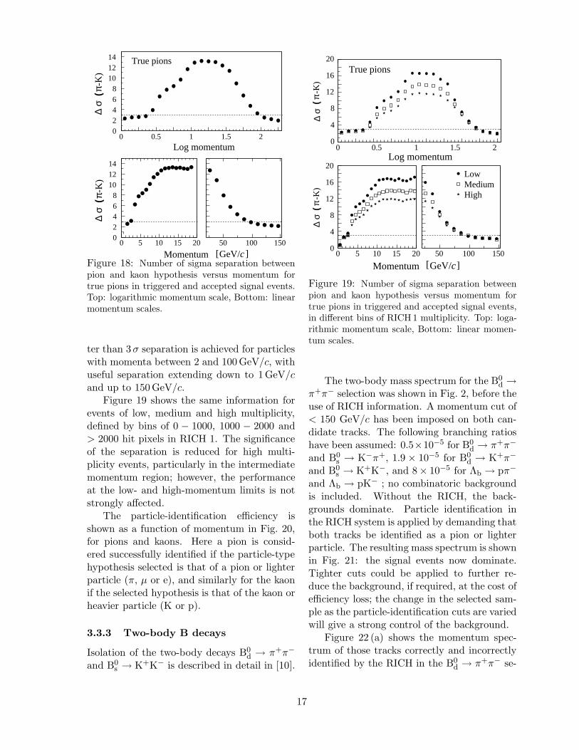
The performance of the RICH reconstructionhas been tested using all of the tracks thatpass through the RICH detectors in simulatedB0
d → π+π− events. The results are shown in
Table 3. Each track gives a single entry: thecolumn gives the true particle type (or X if thetrack is below threshold in all radiators) andthe row gives the reconstructed particle type(or X if the track is reconstructed as beingbelow threshold in all radiators). The perfor-mance can be quantified in terms of the ef-ficiency ε (the fraction of true particles of agiven type that are identified correctly) andthe purity P (the fraction of tracks that havebeen identified as a given particle type thatare truly that type). As can be seen, the ef-ficiencies are typically better than 80%. Thepurities are also high, except for muons, whichsuffer from significant pion contamination dueto the much larger number of pion tracks (closein mass to the muon).
Instead of simply choosing the maximum-likelihood solution, the separation between dif-ferent particle hypotheses can be varied. Thisis expressed in terms of Gaussian sigma us-ing the correspondence Nσ =
√2∆ lnL, where
∆ lnL is the difference in log-likelihood be-tween the two hypotheses (Nσ > 0 for thenominal maximum-likelihood requirement).
Table 3: Results from the global pattern recog-nition applied to well reconstructed tracks in trig-gered and accepted signal events between 1 and 150GeV/c. Each track gives one entry in the table, andX denotes tracks below threshold in all radiators;the rows give the reconstructed particle type, P isthe purity and ε the efficiency. The sample corre-sponds to 500k tracks, but has been renormalisedto 1000.
True particle type
Rec e µ π K p X Pe 97.4 0.7 24.6 1.4 0.5 3.1 0.76µ 4.0 8.7 69.5 2.0 0.5 4.9 0.10π 2.5 1.3 545.7 3.3 0.7 5.1 0.98K 0.3 0.1 12.7 70.6 4.8 4.3 0.76p 0.2 0.0 1.7 4.3 35.9 0.0 0.85X 9.9 0.8 19.8 3.2 0.0 55.6 0.62
ε 0.85 0.76 0.81 0.83 0.85 0.76
Figure 18 shows the average number ofsigma separation versus momentum betweenthe pion and kaon hypotheses for true pionsin triggered and accepted signal events. Bet-
16
02468
101214
0 0.5 1 1.5 2
Log momentum
∆ σ
(π-
K)
True pions
02468
101214
0 5 10 15 20
∆ σ
(π-
K)
50 100 150
Momentum [ GeV/c ]Figure 18: Number of sigma separation betweenpion and kaon hypothesis versus momentum fortrue pions in triggered and accepted signal events.Top: logarithmic momentum scale, Bottom: linearmomentum scales.
ter than 3σ separation is achieved for particleswith momenta between 2 and 100 GeV/c, withuseful separation extending down to 1GeV/cand up to 150 GeV/c.
Figure 19 shows the same information forevents of low, medium and high multiplicity,defined by bins of 0 − 1000, 1000 − 2000 and> 2000 hit pixels in RICH 1. The significanceof the separation is reduced for high multi-plicity events, particularly in the intermediatemomentum region; however, the performanceat the low- and high-momentum limits is notstrongly affected.
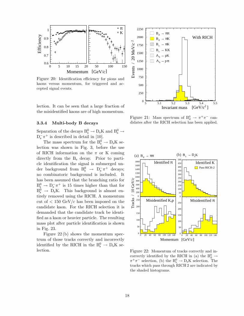
The particle-identification efficiency isshown as a function of momentum in Fig. 20,for pions and kaons. Here a pion is consid-ered successfully identified if the particle-typehypothesis selected is that of a pion or lighterparticle (π, µ or e), and similarly for the kaonif the selected hypothesis is that of the kaon orheavier particle (K or p).
3.3.3 Two-body B decays
Isolation of the two-body decays B0d → π+π−
and B0s → K+K− is described in detail in [10].
0
4
8
12
16
20
0 0.5 1 1.5 2
True pions
Log momentum
∆ σ
(π
-K)
0
4
8
12
16
20
0 5 10 15 20
∆ σ
(π
-K)
50 100 150
Momentum [ GeV/c ]
LowMediumHigh
Figure 19: Number of sigma separation betweenpion and kaon hypothesis versus momentum fortrue pions in triggered and accepted signal events,in different bins of RICH1 multiplicity. Top: loga-rithmic momentum scale, Bottom: linear momen-tum scales.
The two-body mass spectrum for the B0d →
π+π− selection was shown in Fig. 2, before theuse of RICH information. A momentum cut of< 150 GeV/c has been imposed on both can-didate tracks. The following branching ratioshave been assumed: 0.5×10⁻⁵ for B0
d → π+π−
and B0s → K−π+, 1.9 × 10⁻⁵ for B0
d → K+π−
and B0s → K+K−, and 8× 10⁻⁵ for Λb → pπ−
and Λb → pK− ; no combinatoric backgroundis included. Without the RICH, the back-grounds dominate. Particle identification inthe RICH system is applied by demanding thatboth tracks be identified as a pion or lighterparticle. The resulting mass spectrum is shownin Fig. 21: the signal events now dominate.Tighter cuts could be applied to further re-duce the background, if required, at the cost ofefficiency loss; the change in the selected sam-ple as the particle-identification cuts are variedwill give a strong control of the background.
Figure 22 (a) shows the momentum spec-trum of those tracks correctly and incorrectlyidentified by the RICH in the B0
d → π+π− se-
17
0.6
0.7
0.8
0.9
1
0 5 10 15 20
πK
Effi
cien
cy
50 100 150
Momentum [ GeV/c ]
Figure 20: Identification efficiency for pions andkaons versus momentum, for triggered and ac-cepted signal events.
lection. It can be seen that a large fraction ofthe misidentified kaons are of high momentum.
3.3.4 Multi-body B decays
Separation of the decays B0s → DsK and B0
s →D−
s π+ is described in detail in [10].The mass spectrum for the B0
s → DsK se-lection was shown in Fig. 3, before the useof RICH information on the π or K comingdirectly from the Bs decay. Prior to parti-cle identification the signal is submerged un-der background from B0
s → D−s π+ decays;
no combinatoric background is included. Ithas been assumed that the branching ratio forB0
s → D−s π+ is 15 times higher than that for
B0s → DsK. This background is almost en-
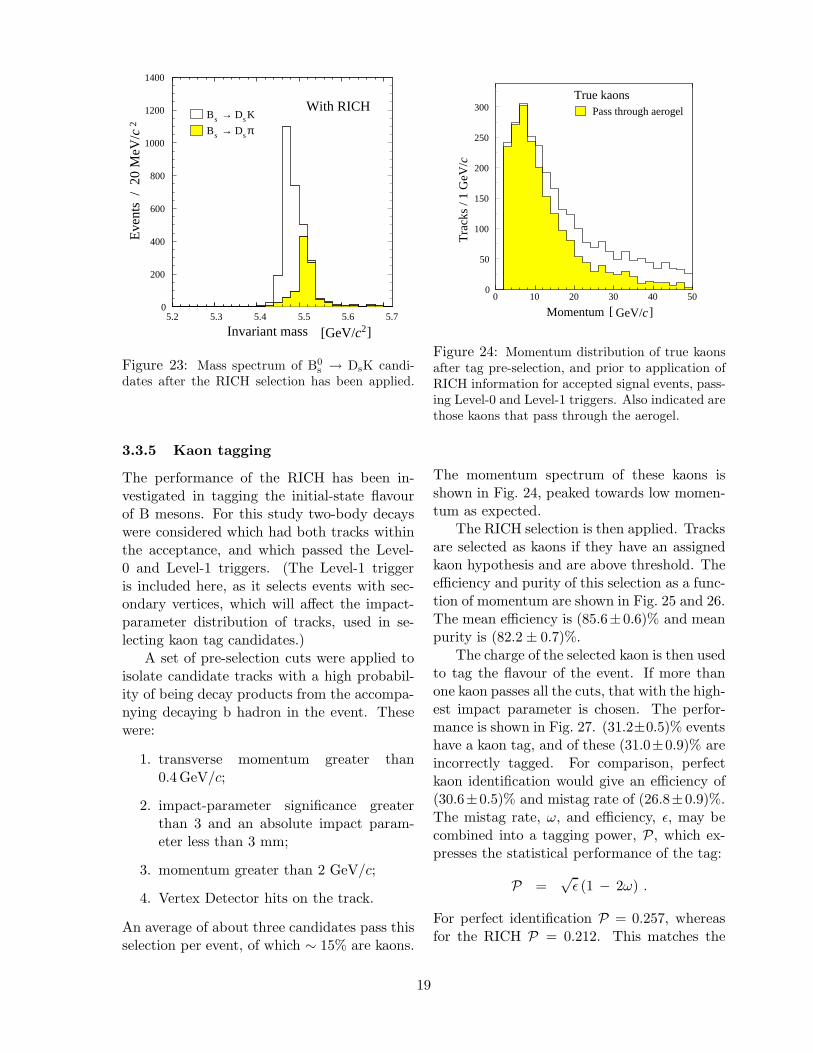
tirely removed using the RICH. A momentumcut of < 150 GeV/c has been imposed on thecandidate kaon. For the RICH selection it isdemanded that the candidate track be identi-fied as a kaon or heavier particle. The resultingmass plot after particle identification is shownin Fig. 23.
Figure 22 (b) shows the momentum spec-trum of those tracks correctly and incorrectlyidentified by the RICH in the B0
s → DsK se-lection.
0
250
500
750
1000
1250
1500
1750
2000
2250
5 5.1 5.2 5.3 5.4 5.5
Invariant mass [GeV/c ] 2
Eve
nts
/ 2
0 M
eV/c
2
With RICHBd → ππBd
b
→ πK
Bs → π
π
K
Bs
→→
KK
pKΛ
b→ pΛ
Figure 21: Mass spectrum of B0d → π+π− can-
didates after the RICH selection has been applied.
Identified KPass RICH-2
Bs → KDs
Misidentified π
Momentum [GeV/c]
(b)
Identified π
Misidentified K,p
Bd → ππ(a)
Tra
cks
/ 1
0 G
eV/c
0
200
400
600
800
1000
1200
1400
1600
1800
0
50
100
150
200
250
0
50
100
150
200
250
300
350
400
450
500
0
50
100
150
200
250
0 20 40 60 80 100 120 140 0 20 40 60 80 100 120 140
Figure 22: Momentum of tracks correctly and in-correctly identified by the RICH in (a) the B0
d →π+π− selection, (b) the B0
s → DsK selection. Thetracks which pass through RICH2 are indicated bythe shaded histograms.
18
0
200
400
600
800
1000
1200
1400
5.2 5.3 5.4 5.5 5.6 5.7
Invariant mass [GeV/c2]
Eve
nts
/ 2
0 M
eV/c2
With RICHBs → DsK
Bs → Dsπ
Figure 23: Mass spectrum of B0s → DsK candi-
dates after the RICH selection has been applied.
3.3.5 Kaon tagging
The performance of the RICH has been in-vestigated in tagging the initial-state flavourof B mesons. For this study two-body decayswere considered which had both tracks withinthe acceptance, and which passed the Level-0 and Level-1 triggers. (The Level-1 triggeris included here, as it selects events with sec-ondary vertices, which will affect the impact-parameter distribution of tracks, used in se-lecting kaon tag candidates.)
A set of pre-selection cuts were applied toisolate candidate tracks with a high probabil-ity of being decay products from the accompa-nying decaying b hadron in the event. Thesewere:
1. transverse momentum greater than0.4 GeV/c;
2. impact-parameter significance greaterthan 3 and an absolute impact param-eter less than 3 mm;
3. momentum greater than 2 GeV/c;
4. Vertex Detector hits on the track.
An average of about three candidates pass thisselection per event, of which ∼ 15% are kaons.
0
50
100
150
200
250
300
0
Momentum [ GeV/c ]
Tra
cks
/ 1 G
eV/c
True kaonsPass through aerogel
10 20 30 40 50
Figure 24: Momentum distribution of true kaonsafter tag pre-selection, and prior to application ofRICH information for accepted signal events, pass-ing Level-0 and Level-1 triggers. Also indicated arethose kaons that pass through the aerogel.
The momentum spectrum of these kaons isshown in Fig. 24, peaked towards low momen-tum as expected.
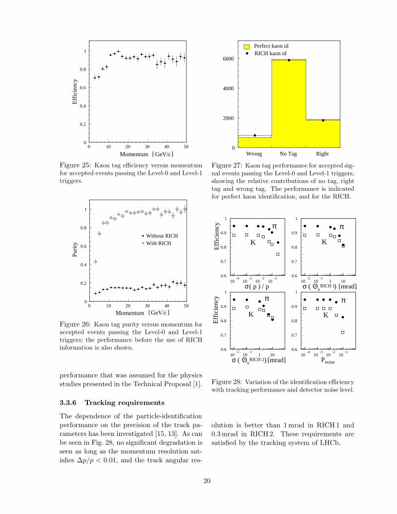
The RICH selection is then applied. Tracksare selected as kaons if they have an assignedkaon hypothesis and are above threshold. Theefficiency and purity of this selection as a func-tion of momentum are shown in Fig. 25 and 26.The mean efficiency is (85.6±0.6)% and meanpurity is (82.2 ± 0.7)%.
The charge of the selected kaon is then usedto tag the flavour of the event. If more thanone kaon passes all the cuts, that with the high-est impact parameter is chosen. The perfor-mance is shown in Fig. 27. (31.2±0.5)% eventshave a kaon tag, and of these (31.0±0.9)% areincorrectly tagged. For comparison, perfectkaon identification would give an efficiency of(30.6±0.5)% and mistag rate of (26.8±0.9)%.The mistag rate, ω, and efficiency, ε, may becombined into a tagging power, P, which ex-presses the statistical performance of the tag:
P =√
ε (1 − 2ω) .
For perfect identification P = 0.257, whereasfor the RICH P = 0.212. This matches the
19
0
0.2
0.4
0.6
0.8
1
0 10 20 30 40 50
Momentum [ GeV/c ]
Effi
cien
cy
Figure 25: Kaon tag efficiency versus momentumfor accepted events passing the Level-0 and Level-1triggers.
0
0.2
0.4
0.6
0.8
1
0 10 20 30 40 50
Momentum [ GeV/c ]
Pur
ity
Without RICHWith RICH
Figure 26: Kaon tag purity versus momentum foraccepted events passing the Level-0 and Level-1triggers; the performance before the use of RICHinformation is also shown.
performance that was assumed for the physicsstudies presented in the Technical Proposal [1].
3.3.6 Tracking requirements
The dependence of the particle-identificationperformance on the precision of the track pa-rameters has been investigated [15, 13]. As canbe seen in Fig. 28, no significant degradation isseen as long as the momentum resolution sat-isfies ∆p/p < 0.01, and the track angular res-
0
2000
4000
6000
Wrong No Tag Right
Perfect kaon id RICH kaon id
Figure 27: Kaon tag performance for accepted sig-nal events passing the Level-0 and Level-1 triggers,showing the relative contributions of no tag, righttag and wrong tag. The performance is indicatedfor perfect kaon identification, and for the RICH.
0.6
0.7
0.8
0.9
1
10-4
10-3
10-2
10-1
σ ( p ) / p
Effi
cien
cy π
K
0.6
0.7
0.8
0.9
1
10-2
10-1
1 10σ ( Θx
RICH 1 ) [mrad]
K
0.6
0.7
0.8
0.9
1
10-2
10-1
1 10σ ( Θx
RICH 2 ) [mrad]
Effi
cien
cy π
K
0.6
0.7
0.8
0.9
1
10-4
10-3
10-2
10-1
P noise
π
π
K
Figure 28: Variation of the identification efficiencywith tracking performance and detector noise level.
olution is better than 1 mrad in RICH1 and0.3 mrad in RICH2. These requirements aresatisfied by the tracking system of LHCb.
20
3.3.7 Future developments
A smooth migration is planned from conven-tional software to a fully object-oriented im-plementation. The basis of the migration isthe new detector analysis environment [17],that allows the use in parallel of code writtenin FORTRAN and new algorithms written inC++.
To ease the migration an object-orientedapproach to the RICH reconstruction has beenstudied, in parallel to the baseline reconstruc-tion program. The development was based onthe unified software development process [18].In a first iteration the problem domain wasanalysed by means of a detailed description ofthe detector and the relevant physics processes.In addition the reconstruction algorithm wasdefined by the baseline program [13]. Whenapplicable, so-called use-cases were applied todescribe important aspects.
Entities most relevant for the reconstruc-tion process have been identified. Their rela-tions have been studied and an object modelhas been developed. It is characterised by so-called “smart” event and detector entities, thatprovide support for a customisable reconstruc-tion algorithm. For example, the track ob-jects can be interrogated not only about simpletrack parameters such as their momentum orangle, but also more complex quantities suchas the length of radiator that they traverse ineach RICH.
Care has been taken to decouple dependen-cies. Event entities within the reconstructionalgorithm are related to the event model ofLHCb by a so-called adapter pattern [19]. Thisconcept provides smart entities for the recon-struction, whilst shielding the reconstructionenvironment from development of the globalevent model.
In a similar way the actual reconstructionalgorithm is implemented by a strategy pat-tern. This allows a customisable reconstruc-tion framework to be developed, that can beused in the future for the implementation ofdifferent algorithms.
Currently the development has reached a
state that allows a comparison to be madewith the results presented in the Technical Pro-posal [1]. As an important step, the physicsperformance and resource consumption havebeen studied and are found to be equiva-lent [20]. A full implementation, consideringthe updated geometry and additional sourcesof detector noise, is foreseen in the near future.
21

4 Prototype results
4.1 Overview
There has been an intensive programme ofdevelopment work undertaken for the LHCbRICH detectors. A summary of the work isdescribed in this section.
Prototypes of the RICH1 and RICH2 de-tectors have been constructed to study a num-ber of important properties of radiators andphotodetectors in a test-beam and in the labo-ratory. These studies include measurement of:
1. The performance of the aerogel radiator,its photon yield, scattering properties,clarity and refractive index;
2. The simultaneous detection ofCherenkov rings from gaseous andaerogel radiators;
3. The characteristics of the C4F10 and CF4
gas radiators, the photon yield and chro-matic properties;
4. The performance of HPD’s for detectingCherenkov photons, the efficiency, andthe resolution of the Cherenkov angle;
5. The detailed electron optics of prototypePixel HPD tubes, including a full-scaletube with 72-18 mm demagnification;
6. The operation of Pixel HPD tubes in thepresence of a magnetic field;
7. The behaviour of the HPD detectorswhen charged particles pass through thedevice.
In addition, a programme of work to evalu-ate the optical characteristics of prototype mir-rors and the stability of their supports is wellunderway. The methods used for measuringthe optical and mechanical properties of mir-rors and supports are also described below.
4.2 Prototype tests
4.2.1 The RICH1 and RICH2 proto-type detectors
The beam tests described here used prototypesof the LHCb RICH1 and RICH2 counters ina number of configurations :
1. A 14 -scale prototype of the RICH1 detec-
tor [21], shown schematically in Fig. 29.The purpose of this prototype was to si-multaneously measure Cherenkov ringsfrom aerogel and gaseous radiators, ei-ther air or C4F10. A 240 mm focal-length mirror reflected the Cherenkovrings onto an array of seven commercial61-pixel Hybrid Photo-Diodes (HPD’s)at the photodetection plane.
2. A full-scale RICH1 prototype was con-structed by adding extension tubes toincrease the gaseous-radiator length to100 cm [21], and to focus the rings ontothe photodetector plane using a 1117 mmfocal-length mirror.
3. A full-scale prototype of the RICH2 [22],is shown schematically in Fig. 30. A4003 mm focal length mirror reflectedCherenkov photons from approximately1.8 m of CF4 gaseous radiator onto anarray of seven HPD’s and a single Multi-Anode Photomultiplier (MAPMT) atthe photodetection plane.
A variety of photodetectors were used inthe beam studies :
1. The 61-pixel HPD manufactured byDEP2. This HPD, shown schematicallyin Fig. 31, has an S20 (trialkali) photo-cathode deposited on a quartz window.Photoelectrons are accelerated througha 12 kV potential onto a 61-pixel silicondetector. This device gives an approxi-mate gain of 3000. The pixels are hexag-onally close packed and measure 2 mm
2Delft Electronische Producten(DEP), The Nether-lands
22
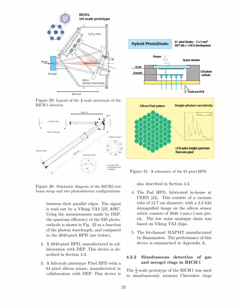
RICH1: 1/4 scale prototype
Aerogel
Beam
C4F10 Gas
Mirror240mm focal length
400 mm
HPD
Rea
d-ou
t Ele
ctro
nics
Figure 29: Layout of the 14 -scale prototype of the
RICH 1 detector.
Detector Setup 1
Detector Setup 2
B
A1 A3
A2
A1A3
A4
C A5A6
A7
A2
X7 Beam line
1800 mm
4000 mmDetector Plate
Silicon Telescope
Mirror
A: 61-pixel HPDB: 2048-pixel HPDC: MAPMT
Figure 30: Schematic diagram of the RICH2 testbeam setup and two photodetector configurations.
between their parallel edges. The signalis read out by a Viking VA2 [23] ASIC.Using the measurements made by DEP,the quantum efficiency of the S20 photo-cathode is shown in Fig. 32 as a functionof the photon wavelength, and comparedto the 2048-pixel HPD (see below).
2. A 2048-pixel HPD, manufactured in col-laboration with DEP. This device is de-scribed in Section 4.3.
3. A full-scale prototype Pixel HPD with a61-pixel silicon sensor, manufactured incollaboration with DEP. This device is
Hybrid PhotoDiode: 61 pixel Diodes : 2 x 2 mm2 DEP (NL) + LHCb development
Single-photon sensitivity
LED pulse height spectrumfrom one pixel
Silicon Pixel pattern
Read-out ASIC
-12 kV
Ground
Quartz window
S20 photocathode
Photon
Figure 31: A schematic of the 61-pixel HPD
also described in Section 4.3.
4. The Pad HPD, fabricated in-house atCERN [24]. This consists of a vacuumtube of 12.7 cm diameter, with a 2.3 folddemagnified image on the silicon sensorwhich consists of 2048 1mm×1mm pix-els. The low noise analogue chain wasbased on Viking VA3 chips.
5. The 64-channel MAPMT manufacturedby Hamamatsu. The performance of thisdevice is summarized in Appendix A.
4.2.2 Simultaneous detection of gasand aerogel rings in RICH1
The 14 -scale prototype of the RICH1 was used
to simultaneously measure Cherenkov rings
23
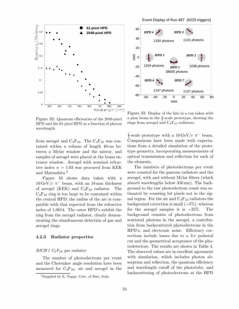
61-pixel HPD2048-pixel HPD
Figure 32: Quantum efficiencies of the 2048-pixelHPD and the 61-pixel HPD as a function of photonwavelength.
from aerogel and C4F10. The C4F10 was con-tained within a volume of length 40 cm be-tween a Mylar window and the mirror, andsamples of aerogel were placed at the beam en-trance window. Aerogel with nominal refrac-tive index n = 1.03 was procured from KEKand Matsushita.3
Figure 33 shows data taken with a10GeV/c π− beam, with an 18 mm thicknessof aerogel (KEK) and C4F10 radiator. TheC4F10 ring is too large to be contained withinthe central HPD; the radius of the arc is com-patible with that expected from the refractiveindex of 1.0014. The outer HPD’s exhibit thering from the aerogel radiator, clearly demon-strating the simultaneous detection of gas andaerogel rings.
4.2.3 Radiator properties
RICH 1 C4F10 gas radiator
The number of photoelectrons per eventand the Cherenkov angle resolution have beenmeasured for C4F10, air and aerogel in the
3Supplied by E. Nappi, Univ. of Bari, Italy.
Event Display of Run 487 (6225 triggers)
-80
-60
-40
-20
0
20
40
60
-60 -40 -20 0 20 40 60 80mm
mm
HPD 138605 photons
HPD 2
1038 photons
HPD 3
1131 photons
HPD 4
1320 photons
HPD 5
1204 photons
HPD 6 HPD 7
1147 photons 1137 photons
Figure 33: Display of the hits in a run taken witha pion beam in the 1
4 -scale prototype, showing therings from aerogel and C4F10 radiators.
14 -scale prototype with a 10GeV/c π− beam.Comparisons have been made with expecta-tions from a detailed simulation of the proto-type geometry, incorporating measurements ofoptical transmission and reflection for each ofthe elements.
The numbers of photoelectrons per eventwere counted for the gaseous radiators and theaerogel, with and without Mylar filters (whichabsorb wavelengths below 350 nm). The back-ground to the raw photoelectron count was es-timated by counting hit pixels not in the sig-nal region. For the air and C4F10 radiators thebackground correction is small (∼5%), whereasfor the aerogel samples it is ∼25%. Thebackground consists of photoelectrons fromscattered photons in the aerogel, a contribu-tion from backscattered photoelectrons in theHPD’s, and electronic noise. Efficiency cor-rections include losses due to a 3 σ pedestalcut and the geometrical acceptance of the pho-todetectors. The results are shown in Table 4.The observed values are in excellent agreementwith simulation, which includes photon ab-sorption and reflection, the quantum efficiencyand wavelength cutoff of the phototube, andbackscattering of photoelectrons at the HPD
24
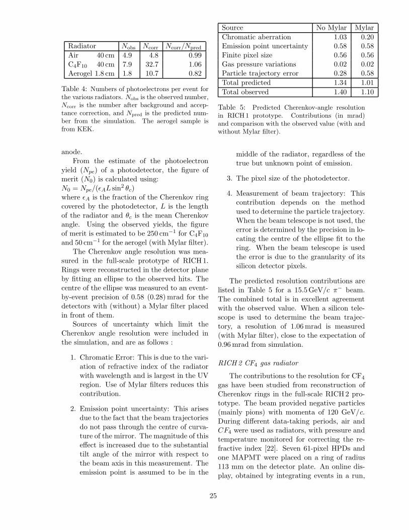
Radiator Nobs Ncorr Ncorr/Npred
Air 40 cm 4.9 4.8 0.99C4F10 40 cm 7.9 32.7 1.06Aerogel 1.8 cm 1.8 10.7 0.82
Table 4: Numbers of photoelectrons per event forthe various radiators. Nobs is the observed number,Ncorr is the number after background and accep-tance correction, and Npred is the predicted num-ber from the simulation. The aerogel sample isfrom KEK.
anode.From the estimate of the photoelectron
yield (Npe) of a photodetector, the figure ofmerit (N0) is calculated using:N0 = Npe/(εAL sin2 θc)where εA is the fraction of the Cherenkov ringcovered by the photodetector, L is the lengthof the radiator and θc is the mean Cherenkovangle. Using the observed yields, the figureof merit is estimated to be 250 cm−1 for C4F10
and 50 cm−1 for the aerogel (with Mylar filter).The Cherenkov angle resolution was mea-
sured in the full-scale prototype of RICH1.Rings were reconstructed in the detector planeby fitting an ellipse to the observed hits. Thecentre of the ellipse was measured to an event-by-event precision of 0.58 (0.28) mrad for thedetectors with (without) a Mylar filter placedin front of them.
Sources of uncertainty which limit theCherenkov angle resolution were included inthe simulation, and are as follows :
1. Chromatic Error: This is due to the vari-ation of refractive index of the radiatorwith wavelength and is largest in the UVregion. Use of Mylar filters reduces thiscontribution.
2. Emission point uncertainty: This arisesdue to the fact that the beam trajectoriesdo not pass through the centre of curva-ture of the mirror. The magnitude of thiseffect is increased due to the substantialtilt angle of the mirror with respect tothe beam axis in this measurement. Theemission point is assumed to be in the
Source No Mylar MylarChromatic aberration 1.03 0.20Emission point uncertainty 0.58 0.58Finite pixel size 0.56 0.56Gas pressure variations 0.02 0.02Particle trajectory error 0.28 0.58Total predicted 1.34 1.01Total observed 1.40 1.10
Table 5: Predicted Cherenkov-angle resolutionin RICH1 prototype. Contributions (in mrad)and comparison with the observed value (with andwithout Mylar filter).
middle of the radiator, regardless of thetrue but unknown point of emission.
3. The pixel size of the photodetector.
4. Measurement of beam trajectory: Thiscontribution depends on the methodused to determine the particle trajectory.When the beam telescope is not used, theerror is determined by the precision in lo-cating the centre of the ellipse fit to thering. When the beam telescope is usedthe error is due to the granularity of itssilicon detector pixels.
The predicted resolution contributions arelisted in Table 5 for a 15.5GeV/c π− beam.The combined total is in excellent agreementwith the observed value. When a silicon tele-scope is used to determine the beam trajec-tory, a resolution of 1.06 mrad is measured(with Mylar filter), close to the expectation of0.96 mrad from simulation.
RICH 2 CF4 gas radiator
The contributions to the resolution for CF4
gas have been studied from reconstruction ofCherenkov rings in the full-scale RICH2 pro-totype. The beam provided negative particles(mainly pions) with momenta of 120 GeV/c.During different data-taking periods, air andCF4 were used as radiators, with pressure andtemperature monitored for correcting the re-fractive index [22]. Seven 61-pixel HPDs andone MAPMT were placed on a ring of radius113 mm on the detector plate. An online dis-play, obtained by integrating events in a run,
25
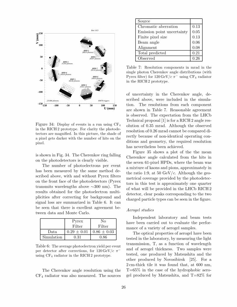
-150
-100
-50
0
50
100
150
-150 -100 -50 0 50 100 150
Run 1415
80878 triggers235486 photons
HPD 126047 photons
HPD 228819 photons
HPD 331293 photons
HPD 424634 photons
HPD 533921 photons
HPD 624410 photons
HPD 728116 photons
PMT 138246 photons
U (mm)
V (
mm
)
Figure 34: Display of events in a run using CF4
in the RICH2 prototype. For clarity the photode-tectors are magnified. In this picture, the shade ofa pixel gets darker with the number of hits on thepixel.
is shown in Fig. 34. The Cherenkov ring fallingon the photodetectors is clearly visible.
The number of photoelectrons per eventhas been measured by the same method de-scribed above, with and without Pyrex filterson the front face of the photodetectors (Pyrextransmits wavelengths above ∼300 nm). Theresults obtained for the photoelectron multi-plicities after correcting for background andsignal loss are summarized in Table 6. It canbe seen that there is excellent agreement be-tween data and Monte Carlo.
Pyrex NoFilter Filter
Data 0.29 ± 0.01 0.86 ± 0.03Simulation 0.31 0.86
Table 6: The average photoelectron yield per eventper detector after corrections, for 120GeV/c π−
using CF4 radiator in the RICH2 prototype.
The Cherenkov angle resolution using theCF4 radiator was also measured. The sources
SourceChromatic aberration 0.13Emission point uncertainty 0.05Finite pixel size 0.13Beam angle 0.06Alignment 0.08Total predicted 0.21Observed 0.26
Table 7: Resolution components in mrad in thesingle photon Cherenkov angle distributions (withPyrex filter) for 120GeV/c π− using CF4 radiatorin the RICH2 prototype.
of uncertainty in the Cherenkov angle, de-scribed above, were included in the simula-tion. The resolutions from each componentare shown in Table 7. Reasonable agreementis observed. The expectation from the LHCbTechnical proposal [1] is for a RICH2 angle res-olution of 0.35 mrad. Although the observedresolution of 0.26 mrad cannot be compared di-rectly because of non-identical operating con-ditions and geometry, the required resolutionhas nevertheless been achieved.
Figure 35 shows a plot of the the meanCherenkov angle calculated from the hits inthe seven 61-pixel HPDs, where the beam wasa mixture of kaons and pions, approximately inthe ratio 1:9, at 50 GeV/c. Although the geo-metrical coverage provided by the photodetec-tors in this test is approximately one quarterof what will be provided in the LHCb RICH2detector, clear peaks corresponding to the twocharged particle types can be seen in the figure.
Aerogel studies
Independent laboratory and beam testshave been carried out to evaluate the perfor-mance of a variety of aerogel samples.
The optical properties of aerogel have beentested in the laboratory, by measuring the lighttransmission, T, as a function of wavelengthand of aerogel thickness. Two samples weretested, one produced by Matsushita and theother produced by Novosibirsk [25]. For a2 cm-thick tile it was found that, at 600 nm,T=65% in the case of the hydrophobic aero-gel produced by Matsushita, and T=82% for
26
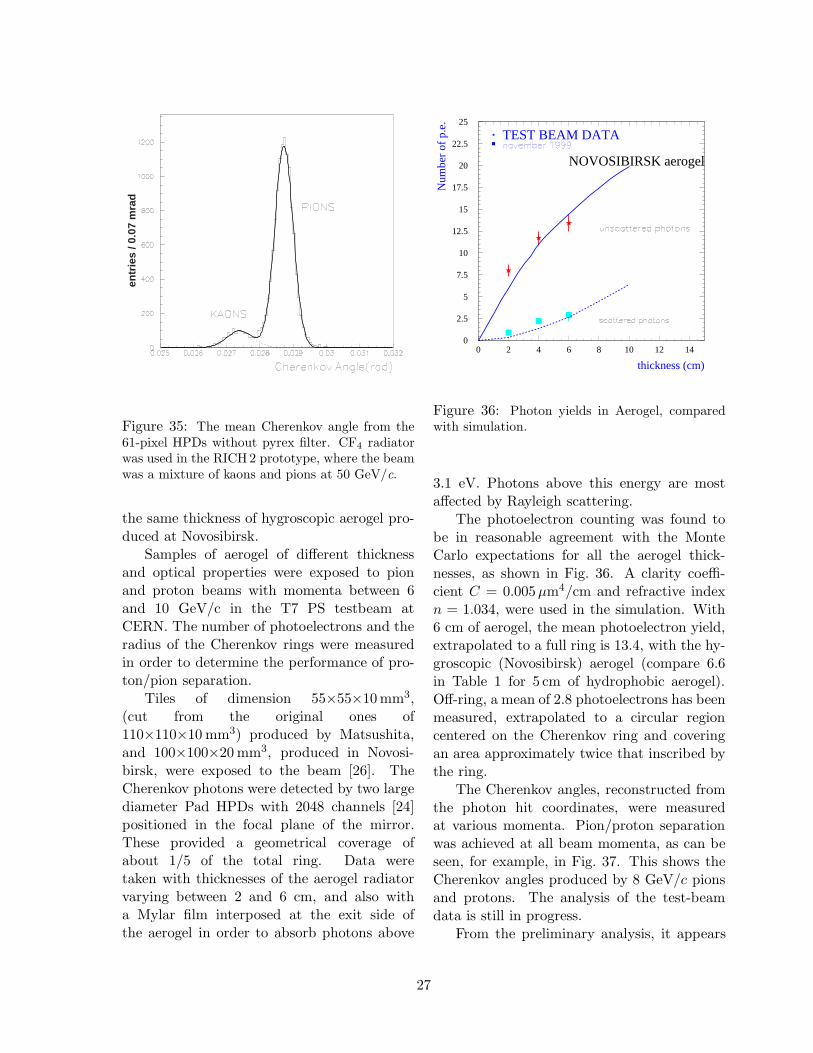
entr
ies
/ 0.0
7 m
rad
Figure 35: The mean Cherenkov angle from the61-pixel HPDs without pyrex filter. CF4 radiatorwas used in the RICH2 prototype, where the beamwas a mixture of kaons and pions at 50 GeV/c.
the same thickness of hygroscopic aerogel pro-duced at Novosibirsk.
Samples of aerogel of different thicknessand optical properties were exposed to pionand proton beams with momenta between 6and 10 GeV/c in the T7 PS testbeam atCERN. The number of photoelectrons and theradius of the Cherenkov rings were measuredin order to determine the performance of pro-ton/pion separation.
Tiles of dimension 55×55×10 mm3,(cut from the original ones of110×110×10 mm3) produced by Matsushita,and 100×100×20 mm3, produced in Novosi-birsk, were exposed to the beam [26]. TheCherenkov photons were detected by two largediameter Pad HPDs with 2048 channels [24]positioned in the focal plane of the mirror.These provided a geometrical coverage ofabout 1/5 of the total ring. Data weretaken with thicknesses of the aerogel radiatorvarying between 2 and 6 cm, and also witha Mylar film interposed at the exit side ofthe aerogel in order to absorb photons above
0
2.5
5
7.5
10
12.5
15
17.5
20
22.5
25
0 2 4 6 8 10 12 14
NOVOSIBIRSK aerogel
thickness (cm)
Num
ber
of p
.e.
TEST BEAM DATA
Figure 36: Photon yields in Aerogel, comparedwith simulation.
3.1 eV. Photons above this energy are mostaffected by Rayleigh scattering.
The photoelectron counting was found tobe in reasonable agreement with the MonteCarlo expectations for all the aerogel thick-nesses, as shown in Fig. 36. A clarity coeffi-cient C = 0.005µm4/cm and refractive indexn = 1.034, were used in the simulation. With6 cm of aerogel, the mean photoelectron yield,extrapolated to a full ring is 13.4, with the hy-groscopic (Novosibirsk) aerogel (compare 6.6in Table 1 for 5 cm of hydrophobic aerogel).Off-ring, a mean of 2.8 photoelectrons has beenmeasured, extrapolated to a circular regioncentered on the Cherenkov ring and coveringan area approximately twice that inscribed bythe ring.
The Cherenkov angles, reconstructed fromthe photon hit coordinates, were measuredat various momenta. Pion/proton separationwas achieved at all beam momenta, as can beseen, for example, in Fig. 37. This shows theCherenkov angles produced by 8 GeV/c pionsand protons. The analysis of the test-beamdata is still in progress.
From the preliminary analysis, it appears
27
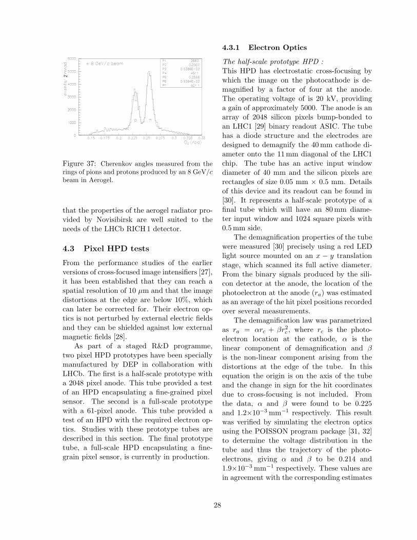
2
Figure 37: Cherenkov angles measured from therings of pions and protons produced by an 8 GeV/cbeam in Aerogel.
that the properties of the aerogel radiator pro-vided by Novisibirsk are well suited to theneeds of the LHCb RICH1 detector.
4.3 Pixel HPD tests
From the performance studies of the earlierversions of cross-focused image intensifiers [27],it has been established that they can reach aspatial resolution of 10 µm and that the imagedistortions at the edge are below 10%, whichcan later be corrected for. Their electron op-tics is not perturbed by external electric fieldsand they can be shielded against low externalmagnetic fields [28].
As part of a staged R&D programme,two pixel HPD prototypes have been speciallymanufactured by DEP in collaboration withLHCb. The first is a half-scale prototype witha 2048 pixel anode. This tube provided a testof an HPD encapsulating a fine-grained pixelsensor. The second is a full-scale prototypewith a 61-pixel anode. This tube provided atest of an HPD with the required electron op-tics. Studies with these prototype tubes aredescribed in this section. The final prototypetube, a full-scale HPD encapsulating a fine-grain pixel sensor, is currently in production.
4.3.1 Electron Optics
The half-scale prototype HPD :This HPD has electrostatic cross-focusing bywhich the image on the photocathode is de-magnified by a factor of four at the anode.The operating voltage of is 20 kV, providinga gain of approximately 5000. The anode is anarray of 2048 silicon pixels bump-bonded toan LHC1 [29] binary readout ASIC. The tubehas a diode structure and the electrodes aredesigned to demagnify the 40 mm cathode di-ameter onto the 11 mm diagonal of the LHC1chip. The tube has an active input windowdiameter of 40 mm and the silicon pixels arerectangles of size 0.05 mm × 0.5 mm. Detailsof this device and its readout can be found in[30]. It represents a half-scale prototype of afinal tube which will have an 80 mm diame-ter input window and 1024 square pixels with0.5 mm side.
The demagnification properties of the tubewere measured [30] precisely using a red LEDlight source mounted on an x − y translationstage, which scanned its full active diameter.From the binary signals produced by the sili-con detector at the anode, the location of thephotoelectron at the anode (ra) was estimatedas an average of the hit pixel positions recordedover several measurements.
The demagnification law was parametrizedas ra = αrc + βr2
c , where rc is the photo-electron location at the cathode, α is thelinear component of demagnification and βis the non-linear component arising from thedistortions at the edge of the tube. In thisequation the origin is on the axis of the tubeand the change in sign for the hit coordinatesdue to cross-focusing is not included. Fromthe data, α and β were found to be 0.225and 1.2×10⁻³ mm−1 respectively. This resultwas verified by simulating the electron opticsusing the POISSON program package [31, 32]to determine the voltage distribution in thetube and thus the trajectory of the photo-electrons, giving α and β to be 0.214 and1.9×10−3 mm−1 respectively. These values arein agreement with the corresponding estimates
28
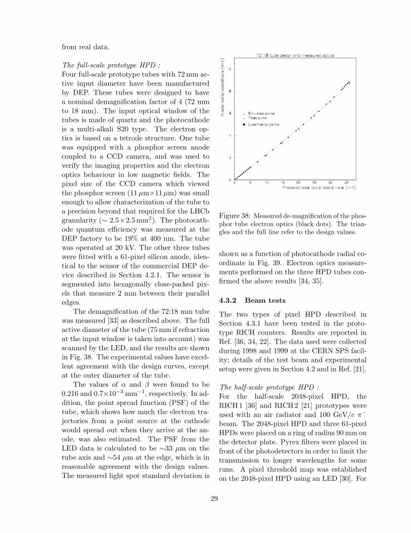
from real data.
The full-scale prototype HPD :Four full-scale prototype tubes with 72 mm ac-tive input diameter have been manufacturedby DEP. These tubes were designed to havea nominal demagnification factor of 4 (72 mmto 18 mm). The input optical window of thetubes is made of quartz and the photocathodeis a multi-alkali S20 type. The electron op-tics is based on a tetrode structure. One tubewas equipped with a phosphor screen anodecoupled to a CCD camera, and was used toverify the imaging properties and the electronoptics behaviour in low magnetic fields. Thepixel size of the CCD camera which viewedthe phosphor screen (11 µm×11µm) was smallenough to allow characterization of the tube toa precision beyond that required for the LHCbgranularity (∼ 2.5×2.5mm2). The photocath-ode quantum efficiency was measured at theDEP factory to be 19% at 400 nm. The tubewas operated at 20 kV. The other three tubeswere fitted with a 61-pixel silicon anode, iden-tical to the sensor of the commercial DEP de-vice described in Section 4.2.1. The sensor issegmented into hexagonally close-packed pix-els that measure 2 mm between their paralleledges.
The demagnification of the 72:18 mm tubewas measured [33] as described above. The fullactive diameter of the tube (75 mm if refractionat the input window is taken into account) wasscanned by the LED, and the results are shownin Fig. 38. The experimental values have excel-lent agreement with the design curves, exceptat the outer diameter of the tube.
The values of α and β were found to be0.216 and 0.7×10⁻³ mm−1, respectively. In ad-dition, the point spread function (PSF) of thetube, which shows how much the electron tra-jectories from a point source at the cathodewould spread out when they arrive at the an-ode, was also estimated. The PSF from theLED data is calculated to be ∼33 µm on thetube axis and ∼54 µm at the edge, which is inreasonable agreement with the design values.The measured light spot standard deviation is
Figure 38: Measured de-magnification of the phos-phor tube electron optics (black dots). The trian-gles and the full line refer to the design values.
shown as a function of photocathode radial co-ordinate in Fig. 39. Electron optics measure-ments performed on the three HPD tubes con-firmed the above results [34, 35].
4.3.2 Beam tests
The two types of pixel HPD described inSection 4.3.1 have been tested in the proto-type RICH counters. Results are reported inRef. [36, 34, 22]. The data used were collectedduring 1998 and 1999 at the CERN SPS facil-ity; details of the test beam and experimentalsetup were given in Section 4.2 and in Ref. [21].
The half-scale prototype HPD :For the half-scale 2048-pixel HPD, theRICH1 [36] and RICH2 [21] prototypes wereused with an air radiator and 100 GeV/c π−
beam. The 2048-pixel HPD and three 61-pixelHPDs were placed on a ring of radius 90 mm onthe detector plate. Pyrex filters were placed infront of the photodetectors in order to limit thetransmission to longer wavelengths for someruns. A pixel threshold map was establishedon the 2048-pixel HPD using an LED [30]. For
29
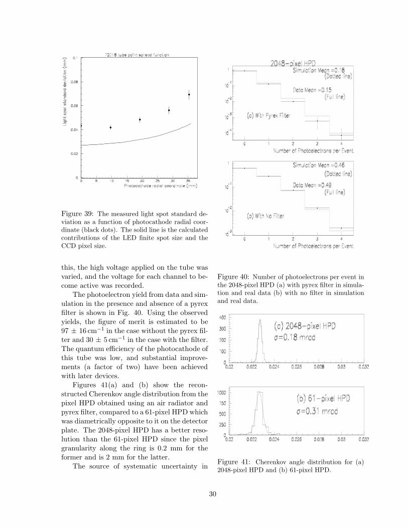
Figure 39: The measured light spot standard de-viation as a function of photocathode radial coor-dinate (black dots). The solid line is the calculatedcontributions of the LED finite spot size and theCCD pixel size.
this, the high voltage applied on the tube wasvaried, and the voltage for each channel to be-come active was recorded.
The photoelectron yield from data and sim-ulation in the presence and absence of a pyrexfilter is shown in Fig. 40. Using the observedyields, the figure of merit is estimated to be97 ± 16 cm−1 in the case without the pyrex fil-ter and 30 ± 5 cm−1 in the case with the filter.The quantum efficiency of the photocathode ofthis tube was low, and substantial improve-ments (a factor of two) have been achievedwith later devices.
Figures 41(a) and (b) show the recon-structed Cherenkov angle distribution from thepixel HPD obtained using an air radiator andpyrex filter, compared to a 61-pixel HPD whichwas diametrically opposite to it on the detectorplate. The 2048-pixel HPD has a better reso-lution than the 61-pixel HPD since the pixelgranularity along the ring is 0.2 mm for theformer and is 2 mm for the latter.
The source of systematic uncertainty in
Figure 40: Number of photoelectrons per event inthe 2048-pixel HPD (a) with pyrex filter in simula-tion and real data (b) with no filter in simulationand real data.
Figure 41: Cherenkov angle distribution for (a)2048-pixel HPD and (b) 61-pixel HPD.
30
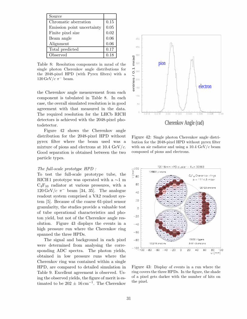
SourceChromatic aberration 0.15Emission point uncertainty 0.05Finite pixel size 0.02Beam angle 0.06Alignment 0.06Total predicted 0.17Observed 0.18
Table 8: Resolution components in mrad of thesingle photon Cherenkov angle distributions forthe 2048-pixel HPD (with Pyrex filters) with a120GeV/c π− beam.
the Cherenkov angle measurement from eachcomponent is tabulated in Table 8. In eachcase, the overall simulated resolution is in goodagreement with that measured in the data.The required resolution for the LHCb RICHdetectors is achieved with the 2048-pixel pho-todetector.
Figure 42 shows the Cherenkov angledistribution for the 2048-pixel HPD withoutpyrex filter where the beam used was amixture of pions and electrons at 10.4 GeV/c.Good separation is obtained between the twoparticle types.
The full-scale prototype HPD :To test the full-scale prototype tube, theRICH1 prototype was operated with a ∼1 mC4F10 radiator at various pressures, with a120 GeV/c π− beam [34, 35]. The analoguereadout system comprised a VA2 readout sys-tem [5]. Because of the coarse 61-pixel sensorgranularity, the studies provide a valuable testof tube operational characteristics and pho-ton yield, but not of the Cherenkov angle res-olution. Figure 43 displays the events in ahigh pressure run where the Cherenkov ringspanned the three HPDs.
The signal and background in each pixelwere determined from analysing the corre-sponding ADC spectra. The photon yields,obtained in low pressure runs where theCherenkov ring was contained within a singleHPD, are compared to detailed simulation inTable 9. Excellent agreement is observed. Us-ing the observed yields, the figure of merit is es-timated to be 202 ± 16 cm−1. The Cherenkov
pion
electron
Cherenkov Angle (rad)
en
trie
s / 0
.1 m
rad
Figure 42: Single photon Cherenkov angle distri-bution for the 2048-pixel HPD without pyrex filterwith an air radiator and using a 10.4 GeV/c beamcomposed of pions and electrons.
Figure 43: Display of events in a run where thering covers the three HPDs. In the figure, the shadeof a pixel gets darker with the number of hits onthe pixel.
31
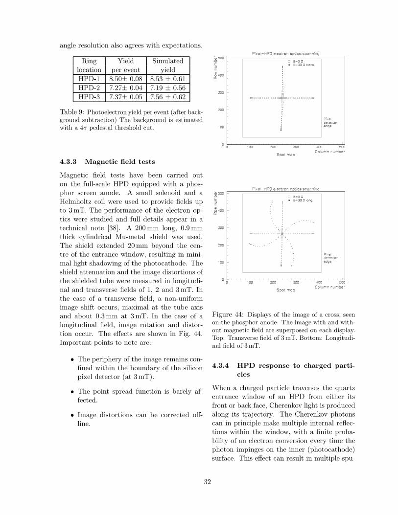
angle resolution also agrees with expectations.
Ring Yield Simulatedlocation per event yieldHPD-1 8.50± 0.08 8.53 ± 0.61HPD-2 7.27± 0.04 7.19 ± 0.56HPD-3 7.37± 0.05 7.56 ± 0.62
Table 9: Photoelectron yield per event (after back-ground subtraction) The background is estimatedwith a 4σ pedestal threshold cut.
4.3.3 Magnetic field tests
Magnetic field tests have been carried outon the full-scale HPD equipped with a phos-phor screen anode. A small solenoid and aHelmholtz coil were used to provide fields upto 3 mT. The performance of the electron op-tics were studied and full details appear in atechnical note [38]. A 200 mm long, 0.9 mmthick cylindrical Mu-metal shield was used.The shield extended 20 mm beyond the cen-tre of the entrance window, resulting in mini-mal light shadowing of the photocathode. Theshield attenuation and the image distortions ofthe shielded tube were measured in longitudi-nal and transverse fields of 1, 2 and 3mT. Inthe case of a transverse field, a non-uniformimage shift occurs, maximal at the tube axisand about 0.3 mm at 3 mT. In the case of alongitudinal field, image rotation and distor-tion occur. The effects are shown in Fig. 44.Important points to note are:
• The periphery of the image remains con-fined within the boundary of the siliconpixel detector (at 3mT).
• The point spread function is barely af-fected.
• Image distortions can be corrected off-line.
Figure 44: Displays of the image of a cross, seenon the phosphor anode. The image with and with-out magnetic field are superposed on each display.Top: Transverse field of 3 mT. Bottom: Longitudi-nal field of 3mT.
4.3.4 HPD response to charged parti-cles
When a charged particle traverses the quartzentrance window of an HPD from either itsfront or back face, Cherenkov light is producedalong its trajectory. The Cherenkov photonscan in principle make multiple internal reflec-tions within the window, with a finite proba-bility of an electron conversion every time thephoton impinges on the inner (photocathode)surface. This effect can result in multiple spu-
32
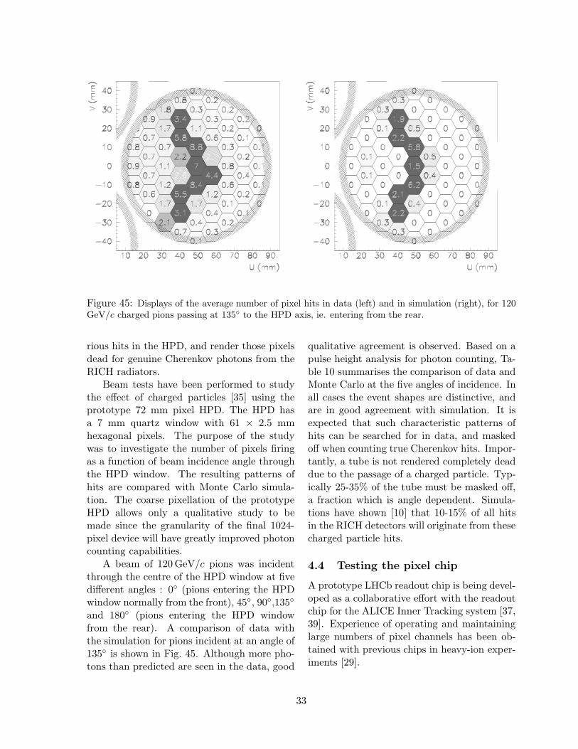
Figure 45: Displays of the average number of pixel hits in data (left) and in simulation (right), for 120GeV/c charged pions passing at 135 to the HPD axis, ie. entering from the rear.
rious hits in the HPD, and render those pixelsdead for genuine Cherenkov photons from theRICH radiators.
Beam tests have been performed to studythe effect of charged particles [35] using theprototype 72 mm pixel HPD. The HPD hasa 7 mm quartz window with 61 × 2.5 mmhexagonal pixels. The purpose of the studywas to investigate the number of pixels firingas a function of beam incidence angle throughthe HPD window. The resulting patterns ofhits are compared with Monte Carlo simula-tion. The coarse pixellation of the prototypeHPD allows only a qualitative study to bemade since the granularity of the final 1024-pixel device will have greatly improved photoncounting capabilities.
A beam of 120 GeV/c pions was incidentthrough the centre of the HPD window at fivedifferent angles : 0 (pions entering the HPDwindow normally from the front), 45, 90,135
and 180 (pions entering the HPD windowfrom the rear). A comparison of data withthe simulation for pions incident at an angle of135 is shown in Fig. 45. Although more pho-tons than predicted are seen in the data, good
qualitative agreement is observed. Based on apulse height analysis for photon counting, Ta-ble 10 summarises the comparison of data andMonte Carlo at the five angles of incidence. Inall cases the event shapes are distinctive, andare in good agreement with simulation. It isexpected that such characteristic patterns ofhits can be searched for in data, and maskedoff when counting true Cherenkov hits. Impor-tantly, a tube is not rendered completely deaddue to the passage of a charged particle. Typ-ically 25-35% of the tube must be masked off,a fraction which is angle dependent. Simula-tions have shown [10] that 10-15% of all hitsin the RICH detectors will originate from thesecharged particle hits.
4.4 Testing the pixel chip
A prototype LHCb readout chip is being devel-oped as a collaborative effort with the readoutchip for the ALICE Inner Tracking system [37,39]. Experience of operating and maintaininglarge numbers of pixel channels has been ob-tained with previous chips in heavy-ion exper-iments [29].
33
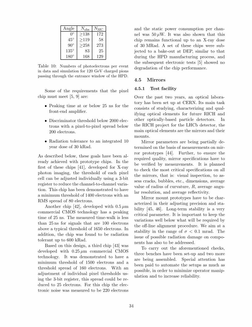
Angle Nobs NMC
0 ≥138 17245 ≥119 5890 ≥258 273
135 83 25180 168 129
Table 10: Numbers of photoelectrons per eventin data and simulation for 120 GeV charged pionspassing through the entrance window of the HPD.
Some of the requirements that the pixelchip must meet [5, 9] are:
• Peaking time at or below 25 ns for thefront-end amplifier.
• Discriminator threshold below 2000 elec-trons with a pixel-to-pixel spread below200 electrons.
• Radiation tolerance to an integrated 10year dose of 30 kRad.
As described below, these goals have been al-ready achieved with prototype chips. In thefirst of these chips [41], developed for X-rayphoton imaging, the threshold of each pixelcell can be adjusted individually using a 3-bitregister to reduce the channel-to-channel varia-tion. This chip has been demonstrated to havea minimum threshold of 1400 electrons with anRMS spread of 80 electrons.
Another chip [42], developed with 0.5 µmcommercial CMOS technology has a peakingtime of 25 ns. The measured time-walk is lessthan 25 ns for signals that are 100 electronsabove a typical threshold of 1650 electrons. Inaddition, the chip was found to be radiationtolerant up to 600 kRad.
Based on this design, a third chip [43] wasdeveloped with 0.25 µm commercial CMOStechnology. It was demonstrated to have aminimum threshold of 1500 electrons and athreshold spread of 160 electrons. With anadjustment of individual pixel thresholds us-ing the 3-bit register, this spread could be re-duced to 25 electrons. For this chip the elec-tronic noise was measured to be 220 electrons
and the static power consumption per chan-nel was 50 µW. It was also shown that thischip remains functional up to an X-ray doseof 30 MRad. A set of these chips were sub-jected to a bake-out at DEP, similar to thatduring the HPD manufacturing process, andthe subsequent electronic tests [5] showed nodegradation of the chip performance.
4.5 Mirrors
4.5.1 Test facility
Over the past two years, an optical labora-tory has been set up at CERN. Its main taskconsists of studying, characterizing and qual-ifying optical elements for future RICH andother optically-based particle detectors. Inthe RICH project for the LHCb detector, themain optical elements are the mirrors and theirmounts.
Mirror parameters are being partially de-termined on the basis of measurements on mir-ror prototypes [44]. Further, to ensure therequired quality, mirror specifications have tobe verified by measurements. It is plannedto check the most critical specifications on allthe mirrors, that is: visual inspection, to as-sess cracks, bubbles, etc., dimensions, averagevalue of radius of curvature, R, average angu-lar resolution, and average reflectivity.
Mirror mount prototypes have to be char-acterized in their adjusting precision and sta-bility [45, 46]. Long-term stability is a verycritical parameter. It is important to keep thevariations well below what will be required bythe off-line alignment procedure. We aim at astability in the range of σ < 0.1 mrad. Theissue of possible radiation damage on compo-nents has also to be addressed.
To carry out the aforementioned checks,three benches have been set-up and two moreare being assembled. Special attention hasbeen paid to automate the setups as much aspossible, in order to minimize operator manip-ulation and to increase reliability.
34
4.5.2 Mirror quality
Each spherical mirror will be tested for its ra-dius of curvature and average angular preci-sion before installation inside the RICH ves-sel. The setup measures the variation fromthe ideal mirror spherical surface by imaginga point source reflected from the sample mir-ror and by analyzing the size and shape of theresulting focal spot. Thus, it provides a di-rect measurement of R and the average angu-lar precision σθ [44].
By measuring a sample of mirrors, we willobtain a distribution in R. For RICH2, itsstandard deviation should not exceed
σR =σd
rc − σd∼ 1.0% of R,
where σd is the photodetector precision and rc
the Cherenkov cone base radius.If the mirror had a perfect spherical sur-
face, the spot on the focal plane should havethe same dimensions as the point source,as the measurement is intrinsically sphericalaberration-free. However, geometrical distor-tions can be present for mirrors with largesurfaces (≥0.10 m2) and thin substrates (≤7 mm). These distortions should be distin-guished from polishing imperfections, whichgreatly depend on the hardness of the sub-strate and also generate poor optical quality.The net result is an enlargement of the focalspot with the presence of irregularities on theborders. We will therefore define that a circlein the focal plane which contains 95% of thereflected light has a diameter D0 = 4σs whereσs is the RMS of the spot size.
We have tested 40 RICH mirror prototypesand provided feedback to the mirror manufac-turers. In Fig. 46, the fraction of reflected lightfalling into circles of different diameters for amirror prototype is shown. In Fig. 47, the di-ameter D0 of the light spot is shown as a func-tion of the distance d of the light spot fromthe mirror surface for different light fractionsinside the circle [44]. These measurements per-mit the precise calculation of R and σθ, whichare equal to 6644 mm and to 0.026 mrad re-spectively for this mirror.
Figure 46: Light fraction inside circles of differentdiameters. Shown is the corresponding D0.
D (
d) [m
m]
0
Figure 47: Spot size as a function of distance dfor a COMPASS mirror. This demonstrates theprocedure for finding the radius of curvature.
Mirror quality has been improving withtime and the measurements performed allowus to conclude that mirrors with a Simax glasssubstrate, a thickness of 6 to 7 mm, a ra-dius of curvature of 8m and a diameter up to∼500 mm are feasible with the geometrical re-quirement of σθ = 0.03 mrad. That is, theyare capable of focussing 95% of the reflectedlight into a circle with diameter D0 = 2mmat the plane defined by the mirror radius ofcurvature R = 8m. Finally, two effects on themirror geometrical quality have yet to be care-fully analyzed: the influence of the final mirrormount and the mirror long-term behaviour.
Spectral reflectivity is another parameterthat is measured in the CERN optical labora-tory to qualify RICH mirrors. In order to min-imize mirror manipulation, we incorporate thereflectivity measurement into the same benchas for the previous set-up. It makes use of ahand-held spectrophotometer and it enables us
35
Tilt
[mra
d]
Figure 48: Mirror support horizontal tilt (arbitary zero). Shown in the insert is the strong mechanicalrelaxation observed at the start of the measurement.
to measure in the wavelength range from 200to 850 nm.
4.5.3 Mirror supports
Two set-ups for the evaluation of the adjust-ment characteristics and the long-term stabil-ity of mirror mounts were developed. Thedetailed principles and results can be foundin [45, 46]. A few mount prototypes have beentested and in particular the one retained forRICH2, which is based on the membrane prin-ciple and it is exclusively made out of Poly-carbonate material [45]. In Fig. 48, its longterm stability is shown by means of the moni-toring of its tilt chart during over 5000 hours.The vertical and horizontal tilts stay well intothe 0.03 mrad required. However, the 1.7 kgweight loaded on the mount simulates a smallermirror than that foreseen for RICH2, there-fore a measurement with a heavier weight hasstarted.
The mount alignment precision is shown inFig. 49 [46]. The adjustment range is 3mrad,which should be sufficient for the machinedmounting holes in the supporting structure. Atilt change of 0.1 mrad corresponds to a screw
turn of 36, which enables a sufficiently pre-cise adjustment. The relationship between tiltand screw-turn is nearly linear4. The RMS ofthe parasitic coupling, crosstalk between thehorizontal and the vertical movement, was lessthan 0.01 mrad.
Vert
ical
adj
ustm
ent [
mra
d]
Figure 49: Results from the mount prototype.The measurement was repeated twice. A linear fitto the measurement is shown.
4The screw used had a pitch of 0.7 mm, that meansa displacement of the wedge of 0.0875 mm for 45 turn.
36
5 Technical Design
5.1 Pixel HPD Photon Detector
The photodetector planes of the RICH detec-tors cover a total area of 2.6m2 over whichit is necessary to detect single photons witha high efficiency and with spatial granularityof about 2.5mm×2.5mm. The photodetectorsneed to be sensitive to Cherenkov light at vis-ible and UV wavelengths and readout must befast, compatible with the 25 ns time betweenLHC bunch crossings and the overall LHCbreadout scheme [8]. The photodetectors will besituated in the fringe field of the spectrometermagnet and will experience a radiation dose ofup to 3 kRad/year.
The baseline photodetector technology se-lected for the LHCb RICH is the Pixel hybridphoton detector (HPD) which uses a silicon de-tector anode inside the vacuum envelope. Pho-toelectons released by photons incident on thephotocathode are accelerated onto the siliconsensor by an applied high voltage ∼ 20 kV,resulting in a signal ∼ 5000 e in the silicon.This device, shown schematically in Fig. 9,has been developed commercially, in a long-standing collaboration with DEP. It is basedon an image intensifier technology, employingelectrostatic cross-focussing to accelerate andimage photoelectrons from the photocathodeonto the anode, demagnifying by a factor ∼ 5.The anode assembly comprises a segmented sil-icon pixel sensor which is bump-bonded to apixel readout chip. This assembly is encap-sulated within the vacuum tube and must becompatible with the bake-out and other fea-tures of the vacuum tube and photocathodedeposition process. During LHCb operation atnominal luminosity the channel occupancy ofthe photodetectors due to Cherenkov photonsis typically 1%, and the probability of multi-photon hits is low. This has permitted theuse of a binary readout scheme, with conse-quent low power consumption and simplifica-tions in the electronics chain between detectorand DAQ.
As described in Sections 4.2–4.4, all fea-
Figure 50: A prototype 80 mm HPD, producedby DEP. The 61-pixel PGA is seen reflected by amirror placed behind the tube.
tures of this pixel HPD have been tested in pro-totypes. Full-scale devices with external read-out electronics (see Fig. 50) have been used toverify the electron optics and to measure thedetected photon yield from Cherenkov lightproduced by charged particle beams. A half-scale device, with encapsulated pixel electron-ics has similarly been used to detect Cherenkovrings in a test beam. The current sched-ule for the development project foresees anLHC-speed pixel readout chip in operation be-fore end 2000. This will be encapsulated ina full-scale HPD. Rigorous performance crite-ria have been defined as a milestone for thisHPD; they require >85% efficiency for detec-tion of a photoelectron in operational chan-nels, with 95% of channels satisfying this crite-rion. In addition, the threshold set to detect aphotoelectron signal is required to satisfy thefollowing: signal/threshold >2.5, and thresh-old/noise >6. The schedule for this milestoneis discussed in Section 6. The implementationof an alternative, backup photodetector tech-nology using commercial metal channel multi-
Table 11: Measured quantum efficiency (Q) atgiven wavelengths λ for a thin-S20 multi-alkali pho-tocathode deposited on a 7 mm-thick quartz win-dow.
λ (nm) 200 240 270 400 600Q (%) 10.2 22.0 25.7 19.3 4.3
37
Figure 51: Outline drawing of the Pixel HPD and its magnetic shield.
anode photomultipliers (Hamamatsu R7600-03-M64 MAPMT), equipped with hemispheri-cal quartz lenses to increase the active area, isdescribed in Appendix A.
Technical details of the Pixel HPD andits readout electronics are summarized inthe following sections. More details on thePixel HPD [5], the readout chip [9] and theMAPMT [6] can be found in LHCb notes.
5.1.1 Vacuum tube and electron optics
The vacuum tube is assembled from metal (ko-var) and ceramic sections as shown in Fig 51.The entrance window is made from 7mm-thickquartz. It is spherical in shape and has a thin-S20 multi-alkali photocathode deposited on itsinner surface. The quantum efficiency (Q) wasmeasured on a prototype tube and values arelisted in Table 11, and result in an energy inte-grated efficiency
∫QdE = 0.77 eV. Cherenkov
photons can be detected over an active diame-
ter of 75mm and the overall diameter is 83mm,resulting in an active area fraction of 0.82.
Photoelectrons are focussed using thetetrode structure shown in Fig. 51. The nom-inal voltage at the photocathode is −20 kV. A300V potential difference between the photo-cathode and first electrode defines the magnifi-cation. The radial coordinate ra (expressed inmm) at the anode is related to the coordinateat the cathode window, rc by
ra = 0.200rc − (4 × 10⁻⁴)r2c .
Taking into account the lensing effect of theentrance window the 0.5mm square anode pix-els correspond to 2.62mm on the tube axis and2.82 mm at the periphery. The RMS pointspread function is approximately constant overthe entrance window and equal to 0.4mm.
The performance of the electron optics wasmeasured using a full-scale prototype tubeequipped with a phosphor anode coupled toa CCD. These measurements were described
38
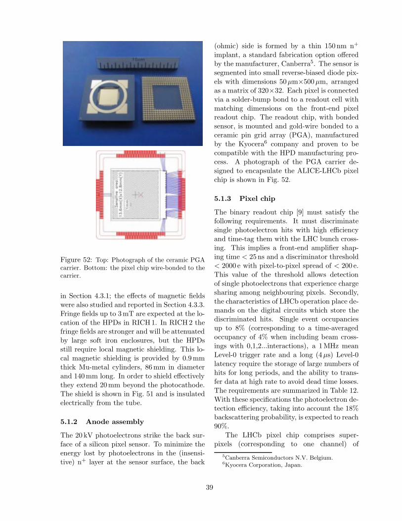
Figure 52: Top: Photograph of the ceramic PGAcarrier. Bottom: the pixel chip wire-bonded to thecarrier.
in Section 4.3.1; the effects of magnetic fieldswere also studied and reported in Section 4.3.3.Fringe fields up to 3mT are expected at the lo-cation of the HPDs in RICH1. In RICH2 thefringe fields are stronger and will be attenuatedby large soft iron enclosures, but the HPDsstill require local magnetic shielding. This lo-cal magnetic shielding is provided by 0.9mmthick Mu-metal cylinders, 86mm in diameterand 140mm long. In order to shield effectivelythey extend 20mm beyond the photocathode.The shield is shown in Fig. 51 and is insulatedelectrically from the tube.
5.1.2 Anode assembly
The 20 kV photoelectrons strike the back sur-face of a silicon pixel sensor. To minimize theenergy lost by photoelectrons in the (insensi-tive) n+ layer at the sensor surface, the back
(ohmic) side is formed by a thin 150 nm n+
implant, a standard fabrication option offeredby the manufacturer, Canberra5. The sensor issegmented into small reverse-biased diode pix-els with dimensions 50µm×500µm, arrangedas a matrix of 320×32. Each pixel is connectedvia a solder-bump bond to a readout cell withmatching dimensions on the front-end pixelreadout chip. The readout chip, with bondedsensor, is mounted and gold-wire bonded to aceramic pin grid array (PGA), manufacturedby the Kyocera6 company and proven to becompatible with the HPD manufacturing pro-cess. A photograph of the PGA carrier de-signed to encapsulate the ALICE-LHCb pixelchip is shown in Fig. 52.
5.1.3 Pixel chip
The binary readout chip [9] must satisfy thefollowing requirements. It must discriminatesingle photoelectron hits with high efficiencyand time-tag them with the LHC bunch cross-ing. This implies a front-end amplifier shap-ing time < 25 ns and a discriminator threshold< 2000 e with pixel-to-pixel spread of < 200 e.This value of the threshold allows detectionof single photoelectrons that experience chargesharing among neighbouring pixels. Secondly,the characteristics of LHCb operation place de-mands on the digital circuits which store thediscriminated hits. Single event occupanciesup to 8% (corresponding to a time-averagedoccupancy of 4% when including beam cross-ings with 0,1,2...interactions), a 1MHz meanLevel-0 trigger rate and a long (4µs) Level-0latency require the storage of large numbers ofhits for long periods, and the ability to trans-fer data at high rate to avoid dead time losses.The requirements are summarized in Table 12.With these specifications the photoelectron de-tection efficiency, taking into account the 18%backscattering probability, is expected to reach90%.
The LHCb pixel chip comprises super-pixels (corresponding to one channel) of
5Canberra Semiconductors N.V. Belgium.6Kyocera Corporation, Japan.
39
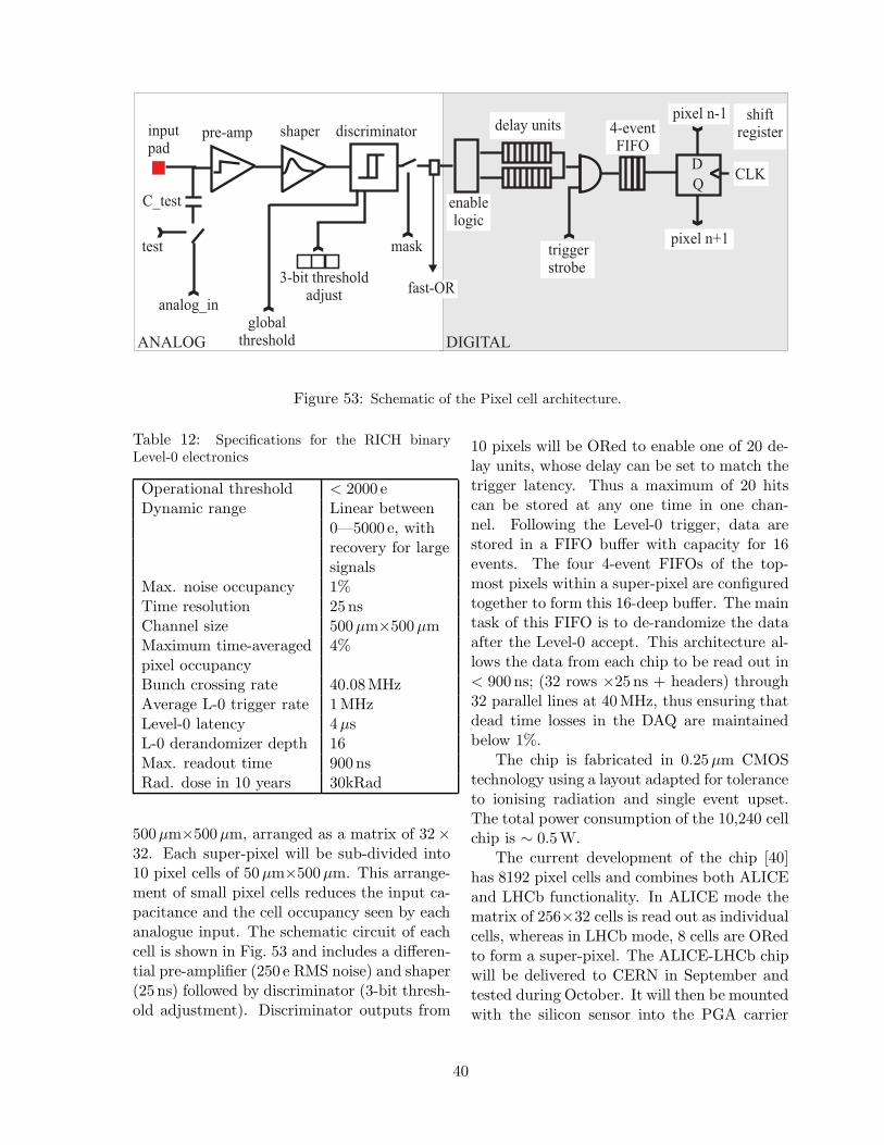
Figure 53: Schematic of the Pixel cell architecture.
Table 12: Specifications for the RICH binaryLevel-0 electronics
Operational threshold < 2000 eDynamic range Linear between
0—5000 e, withrecovery for largesignals
Max. noise occupancy 1%Time resolution 25 nsChannel size 500µm×500µmMaximum time-averaged 4%pixel occupancyBunch crossing rate 40.08MHzAverage L-0 trigger rate 1MHzLevel-0 latency 4µsL-0 derandomizer depth 16Max. readout time 900 nsRad. dose in 10 years 30kRad
500µm×500µm, arranged as a matrix of 32×32. Each super-pixel will be sub-divided into10 pixel cells of 50µm×500µm. This arrange-ment of small pixel cells reduces the input ca-pacitance and the cell occupancy seen by eachanalogue input. The schematic circuit of eachcell is shown in Fig. 53 and includes a differen-tial pre-amplifier (250 e RMS noise) and shaper(25 ns) followed by discriminator (3-bit thresh-old adjustment). Discriminator outputs from
10 pixels will be ORed to enable one of 20 de-lay units, whose delay can be set to match thetrigger latency. Thus a maximum of 20 hitscan be stored at any one time in one chan-nel. Following the Level-0 trigger, data arestored in a FIFO buffer with capacity for 16events. The four 4-event FIFOs of the top-most pixels within a super-pixel are configuredtogether to form this 16-deep buffer. The maintask of this FIFO is to de-randomize the dataafter the Level-0 accept. This architecture al-lows the data from each chip to be read out in< 900 ns; (32 rows ×25 ns + headers) through32 parallel lines at 40MHz, thus ensuring thatdead time losses in the DAQ are maintainedbelow 1%.
The chip is fabricated in 0.25µm CMOStechnology using a layout adapted for toleranceto ionising radiation and single event upset.The total power consumption of the 10,240 cellchip is ∼ 0.5W.
The current development of the chip [40]has 8192 pixel cells and combines both ALICEand LHCb functionality. In ALICE mode thematrix of 256×32 cells is read out as individualcells, whereas in LHCb mode, 8 cells are ORedto form a super-pixel. The ALICE-LHCb chipwill be delivered to CERN in September andtested during October. It will then be mountedwith the silicon sensor into the PGA carrier
40
and encapsulated into an HPD. Only minormodifications to this chip are required to meetfully the LHCb specifications. These include:
• Increasing cell matrix to 320 × 32 with10 cells ORed in a super-pixel: Itis desirable to increase the size ofa super-pixel from 425 µm×400µm to500 µm×500µm. The increase from425 µm to 500 µm in the x-direction re-quires a simple spacing of the inputcolumns and end-of-column logic. In they-direction, one option is to add a fur-ther two 50 µm pixel cells within a super-pixel. This will provide four further de-lay units to store hits and is the optimumin terms of performance. Another possi-ble solution, which involves fewer modifi-cations to the current design, would be tomaintain eight cells per super-pixel andincrease the pixel front-end (and the sen-sor) pitch to 62.5 µm. This does, how-ever, restrict the number of delay units to16, and simulations are underway to as-sess the implications, given the estimatedoccupancies. All the modifications de-scribed above may require re-sizing of thebuffers which drive the control signalsacross the chip and up the pixel columns.Measurements of the ALICE/LHCb chipwill provide data on this issue.
• Logic to monitor FIFO and prevent over-flow: The current ALICE/LHCb chip re-lies on external logic to monitor the con-tent of the FIFO buffers. This will beincluded in the final version to preventoverflow of the buffers and control thereadout when events are available.
• Logic to attach bunch-crossing tag todata packet: To ensure correct synchro-nisation between the Level-0 electronicsand the Level-1 boards ∼100 m away, aheader will be added to the data packet.This will take the form of a 12-bit bunchcrossing number, stored on the arrivalof the corresponding Level-0 trigger foreach accepted event. A 12-bit counter
will be implemented on the chip to gen-erate this number.
• Addition of four on-chip DACs to pro-vide bias voltages: The ALICE/LHCbchip requires the magnitude of the front-end calibration pulses to be set by exter-nal DACs. For accurate determination ofthe noise and threshold dispersion, theprecision and range of these signals aresuch that 12-bits are needed. A designfor an 8-bit DAC has been implementedinto the current chip, and it is plannedto use two such DACs to provide the 12-bit range and precision. By modifyingthe output stages of the DACs, one willset a coarse control, and the other a finecontrol.
The possibility of implementing the addi-tional logic and DACs in a separate PILOTchip, external to the HPD, as described in Sec-tion 5.2, is under investigation. This has ad-vantages for the timescale and allows flexibilityin system integration.
5.1.4 Integration
The photodetector arrays will be constructedfrom hexagonal close-packing of the HPDs, in-cluding their Mu-metal magnetic shields. Thepacking pitch is 87mm, resulting in an active-to-total area fraction of 0.67. A total of 430HPDs is required, 168 for RICH1 and 262 forRICH2. Each pair of HPDs is connected via itsPGA to a Level-0 interface board from whichoptical fibre links transmit binary signals tothe Level-1 electronics in the counting room.Configuration of the encapsulated pixel chipsis provided via a JTAG interface which is ser-viced by the LHCb Experiment Control Sys-tem (ECS).
The high voltages for the photocathodeand focussing electrodes are provided from alow-ripple supply with a 250MΩ voltage di-vider. The bleeder current of 80µA exceedsthe average photocathode current by at least104. For redundancy each column of HPDsin RICH1 and each half column (maximum of
41
8) in RICH2 has its own HV supply and biasvoltage for the silicon sensors.
Further details of the off-detector readoutelectronics and the photodetector mountingare included in Sections 5.2—5.4.
5.2 Readout electronics
5.2.1 Overview
The RICH readout system has the followingmajor components :
• The first stage of readout is the binaryfront-end pixel chip, encapsulated insidethe Pixel HPD vacuum envelope, and de-scribed in Section 5.1.3.
• Each pair of pixel chips is connected viathe HPD pin grid arrays to a “Level-0Adapter Board”, mounted on-detector.The adapter board further multiplexesthe data, drives optical data links tothe off-detector (Level-1) electronics, anddistributes clocks and triggers to thefront-end chips. The binary pixel chipand the adapter board are together re-ferred to as the “Level-0” electronics.
• The “Level-1 Readout Board” is located∼100 m away from the detector in thecounting room. This board receivesthe multiplexed data from the adapterboards via the optical links, it buffersand processes the data, and transportsthe data to the LHCb DAQ system.
A schematic of the LHCb readout architec-ture is shown in Fig. 54. Tables 13 and 14 givea summary of the total number of units in thesystem and the Level-0 and Level-1 parame-ters, respectively. These tables will be referredto in the following sections.
The design philosophy of the RICH readouthas been to avoid building customised electron-ics where suitable commercial and/or general-purpose devices are available, except wherea significant gain in simplicity or cost sav-ing can be achieved. The Level-1 electron-ics have higher complexity and have therefore
been moved away from regions of high radia-tion dose into the LHCb counting room. Thiseases accessibility for maintenance, and elim-inates problems of radiation damage and sin-gle event upsets (SEU’s). It also facilitates theuse of radiation-soft Field-Programmable GateArrays (FPGA’s).
LHCb will use the RD12-developed Tim-ing, Trigger and Control Receiver ASIC(TTCrx) [47] to synchronize the front-end elec-tronics to the rest of the LHCb sub-detectorsand for the local distribution of the clocks andtriggers. Downloading configurations to thepixel chip and the adapter board is providedby a JTAG interface [48] which allows read andwrite access to all registers. The JTAG inter-face is serviced via the Experimental ControlSystem (ECS) [49]. The RICH detectors donot contribute to the Level-0 or Level-1 trig-ger decision.
The readout system is designed to allow ef-ficient stand-alone running, calibration, mon-itoring and debugging. These features, to-gether with a full description of the RICHreadout system, are described in Ref. [50].
5.2.2 The Level-0 Adapter Board
The first stage of readout is the binary pixelchip, described in Section 5.1.3. On a Level-0trigger accept, the data from a pair of pixelchips are multiplexed out at a 40 MHz rateas two 32-bit streams to the Level-0 adapterboard. The multiplex grouping of 32 is chosento match the maximum average LHCb Level-0 trigger rate of 1 MHz. There are 84 and136 adapter boards for RICH1 and RICH2,respectively (one for each pair of HPD’s, andfive extra for RICH2 in order to read out singleHPD’s in odd-numbered columns).
The Level-0 adapter board is shownschematically in Fig. 55. The main functionsare:
1. To provide a further multiplex stage forthe data from the Pixel HPD’s and todrive the data via optical links to theLevel-1 electronics. G-Link protocol isa candidate technology.
42
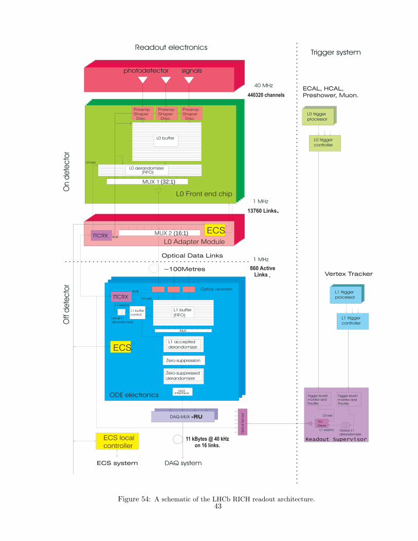
(32:1)
(16:1)
Figure 54: A schematic of the LHCb RICH readout architecture.43
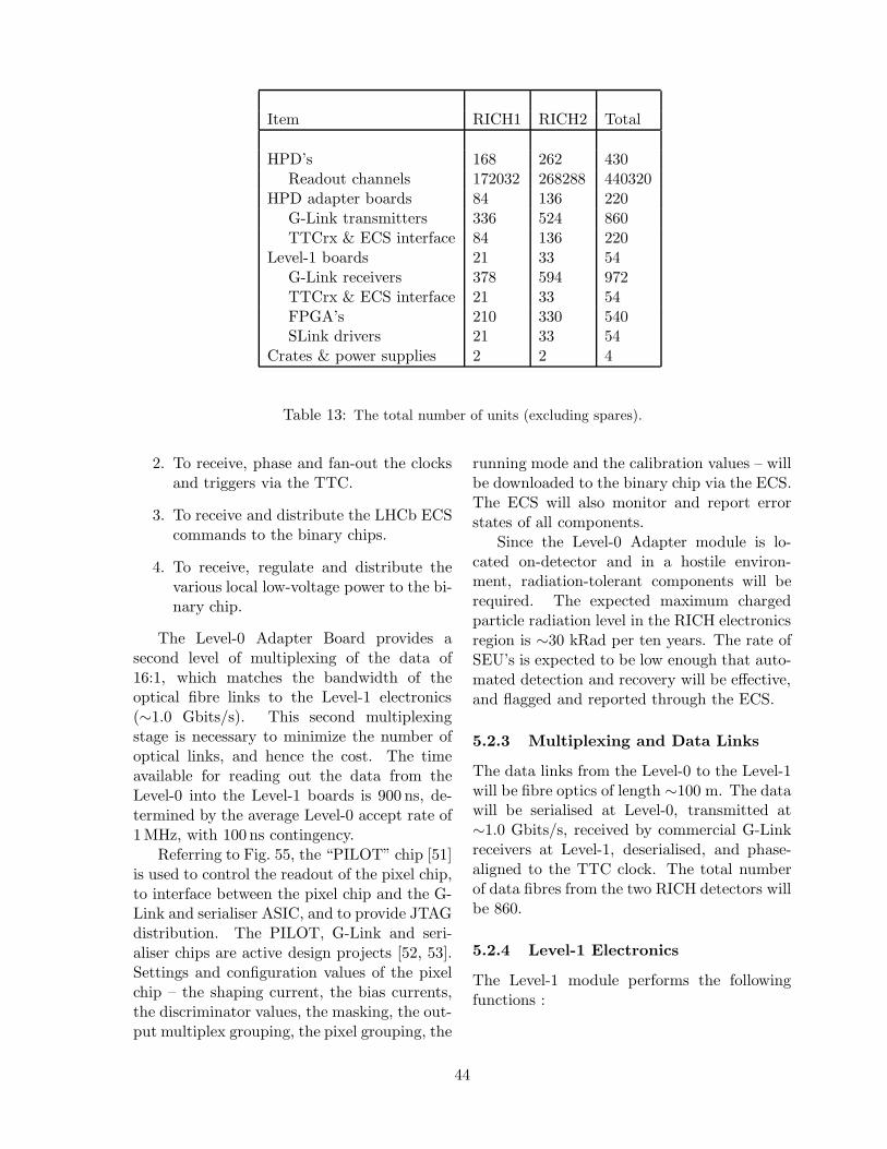
Item RICH1 RICH2 Total
HPD’s 168 262 430Readout channels 172032 268288 440320
HPD adapter boards 84 136 220G-Link transmitters 336 524 860TTCrx & ECS interface 84 136 220
Level-1 boards 21 33 54G-Link receivers 378 594 972TTCrx & ECS interface 21 33 54FPGA’s 210 330 540SLink drivers 21 33 54
Crates & power supplies 2 2 4
Table 13: The total number of units (excluding spares).
2. To receive, phase and fan-out the clocksand triggers via the TTC.
3. To receive and distribute the LHCb ECScommands to the binary chips.
4. To receive, regulate and distribute thevarious local low-voltage power to the bi-nary chip.
The Level-0 Adapter Board provides asecond level of multiplexing of the data of16:1, which matches the bandwidth of theoptical fibre links to the Level-1 electronics(∼1.0 Gbits/s). This second multiplexingstage is necessary to minimize the number ofoptical links, and hence the cost. The timeavailable for reading out the data from theLevel-0 into the Level-1 boards is 900 ns, de-termined by the average Level-0 accept rate of1 MHz, with 100 ns contingency.
Referring to Fig. 55, the “PILOT” chip [51]is used to control the readout of the pixel chip,to interface between the pixel chip and the G-Link and serialiser ASIC, and to provide JTAGdistribution. The PILOT, G-Link and seri-aliser chips are active design projects [52, 53].Settings and configuration values of the pixelchip – the shaping current, the bias currents,the discriminator values, the masking, the out-put multiplex grouping, the pixel grouping, the
running mode and the calibration values – willbe downloaded to the binary chip via the ECS.The ECS will also monitor and report errorstates of all components.
Since the Level-0 Adapter module is lo-cated on-detector and in a hostile environ-ment, radiation-tolerant components will berequired. The expected maximum chargedparticle radiation level in the RICH electronicsregion is ∼30 kRad per ten years. The rate ofSEU’s is expected to be low enough that auto-mated detection and recovery will be effective,and flagged and reported through the ECS.
5.2.3 Multiplexing and Data Links
The data links from the Level-0 to the Level-1will be fibre optics of length ∼100 m. The datawill be serialised at Level-0, transmitted at∼1.0 Gbits/s, received by commercial G-Linkreceivers at Level-1, deserialised, and phase-aligned to the TTC clock. The total numberof data fibres from the two RICH detectors willbe 860.
5.2.4 Level-1 Electronics
The Level-1 module performs the followingfunctions :
44
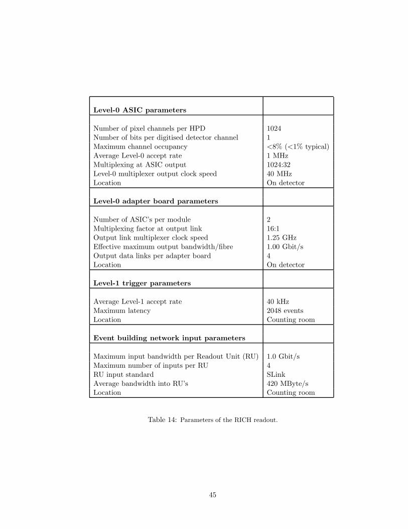
Level-0 ASIC parameters
Number of pixel channels per HPD 1024Number of bits per digitised detector channel 1Maximum channel occupancy <8% (<1% typical)Average Level-0 accept rate 1 MHzMultiplexing at ASIC output 1024:32Level-0 multiplexer output clock speed 40 MHzLocation On detector
Level-0 adapter board parameters
Number of ASIC’s per module 2Multiplexing factor at output link 16:1Output link multiplexer clock speed 1.25 GHzEffective maximum output bandwidth/fibre 1.00 Gbit/sOutput data links per adapter board 4Location On detector
Level-1 trigger parameters
Average Level-1 accept rate 40 kHzMaximum latency 2048 eventsLocation Counting room
Event building network input parameters
Maximum input bandwidth per Readout Unit (RU) 1.0 Gbit/sMaximum number of inputs per RU 4RU input standard SLinkAverage bandwidth into RU’s 420 MByte/sLocation Counting room
Table 14: Parameters of the RICH readout.
45
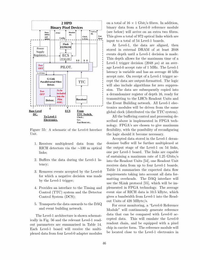
PowerSupply
Regulators..
ReceiverDriver.
G-LinkParallel/serial Fibre
Driver.
PILOT.
TTC
ECSJTAG/IIC
2 HPDBinary Pixel Devices
FlashEEPROM
To Level-1Electronics.
ECSBase LevelDC.
FromTTC Switch.Clock ;Lo ;Fast Reset etc..
Data.HPD1andHPD2
Config.
Monitoretc.
Clock,L-0 etc.
FastReset
TwoOFF
To beincludedinto thePilotASIC.
2 x 32 Lines.
JTAGCal Lo,Hi.
TwoOFF
Figure 55: A schematic of the Level-0 InterfaceUnit.
1. Receives multiplexed data from theRICH detectors via the ∼100 m opticallinks;
2. Buffers the data during the Level-1 la-tency;
3. Removes events accepted by the Level-0for which a negative decision was madeby the Level-1 trigger;
4. Provides an interface to the Timing andControl (TTC) system and the DetectorControl System (DCS);
5. Transports the data onwards to the DAQand event building network.
The Level-1 architecture is shown schemat-ically in Fig. 56 and the relevant Level-1 read-out parameters are summarised in Table 14.Each Level-1 board will receive the multi-plexed data from four Level-0 adapter modules
on a total of 16 × 1 Gbit/s fibres. In addition,binary data from a Level-0 reference module(see below) will arrive on an extra two fibres.This gives a total of 972 optical links which areinput to a total of 54 Level-1 boards.
At Level-1, the data are aligned, thenstored in external DRAM of at least 2048events depth until a Level-1 decision is made.This depth allows for the maximum time of aLevel-1 trigger decision (2048 µs) at an aver-age Level-0 accept rate of 1 MHz. The Level-1latency is variable and has an average 40 kHzaccept rate. On receipt of a Level-1 trigger ac-cept the data are output-formatted. The logicwill also include algorithms for zero suppres-sion. The data are subsequently copied intoa derandomizer register of depth 16, ready fortransmitting to the LHCb Readout Units andthe Event Building network. All Level-1 elec-tronics modules will be driven from the sameglobal clock (distributed via the TTC system).
All the buffering control and processing de-scribed above is implemented in FPGA tech-nology. FPGA’s are chosen to give maximumflexibility, with the possibility of reconfiguringthe logic should it become necessary.
Accepted data stored in the Level-1 deran-domizer buffer will be further multiplexed atthe output stage of the Level-1 on 54 links,one per Level-1 board. The links are capableof sustaining a maximum rate of 1.25 Gbits/sinto the Readout Units [54], one Readout Unitreceives data from up to four Level-1 boards.Table 14 summarises the expected data flowrequirements taking into account all data for-matting overheads. The DAQ interface willuse the SLink protocol [55], which will be im-plemented in FPGA technology. The averageevent size of RICH data is 10.5 kByte, whichgives a bandwidth from Level-1 into the Read-out Units of 420 MByte/s.
For error monitoring, a “Level-0 ReferenceModule” will continuously generate referencedata that can be compared with Level-0 ac-cepted data. This will emulate the Level-0readout chain, and be equipped with a pixelchip in carrier form. The reference module willbe located close to the Level-1 electronics in
46
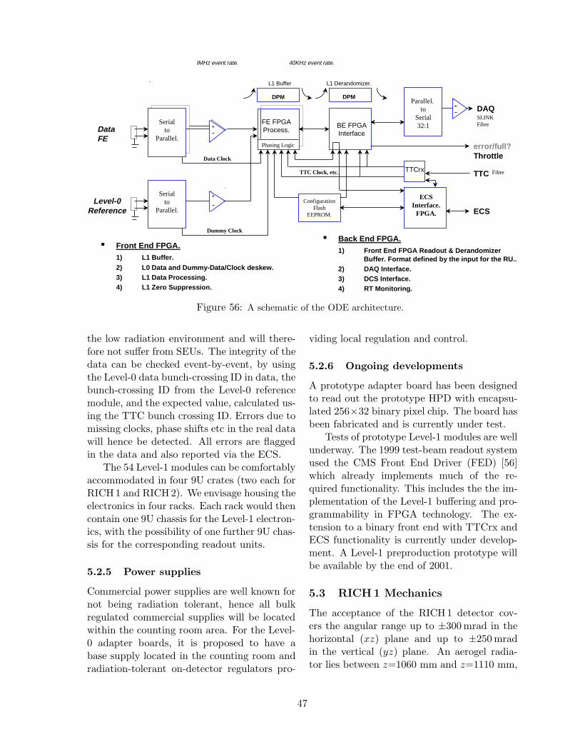
DAQ SLINKFibre
Parallel.to
Serial32:1
.
FE FPGAProcess.
BE FPGAInterfaceData
FE
ECS
TTCrx TTC
error/full?Throttle
• Front End FPGA.1) L1 Buffer.2) L0 Data and Dummy-Data/Clock deskew.3) L1 Data Processing.4) L1 Zero Suppression.
• Back End FPGA.1) Front End FPGA Readout & Derandomizer
Buffer. Format defined by the input for the RU..2) DAQ Interface.3) DCS Interface.4) RT Monitoring.
IMHz event rate. 40KHz event rate.
Level-0Reference
TTC Clock, etc.
Serialto
Parallel.
.
Serialto
Parallel.
Data Clock
Dummy Clock
Phasing Logic
Fibre
ECSInterface.
FPGA.
ConfigurationFlash
EEPROM.
DAQ
L1 Buffer
DPM
L1 Derandomizer.
DPM
+
Figure 56: A schematic of the ODE architecture.
the low radiation environment and will there-fore not suffer from SEUs. The integrity of thedata can be checked event-by-event, by usingthe Level-0 data bunch-crossing ID in data, thebunch-crossing ID from the Level-0 referencemodule, and the expected value, calculated us-ing the TTC bunch crossing ID. Errors due tomissing clocks, phase shifts etc in the real datawill hence be detected. All errors are flaggedin the data and also reported via the ECS.
The 54 Level-1 modules can be comfortablyaccommodated in four 9U crates (two each forRICH1 and RICH2). We envisage housing theelectronics in four racks. Each rack would thencontain one 9U chassis for the Level-1 electron-ics, with the possibility of one further 9U chas-sis for the corresponding readout units.
5.2.5 Power supplies
Commercial power supplies are well known fornot being radiation tolerant, hence all bulkregulated commercial supplies will be locatedwithin the counting room area. For the Level-0 adapter boards, it is proposed to have abase supply located in the counting room andradiation-tolerant on-detector regulators pro-
viding local regulation and control.
5.2.6 Ongoing developments
A prototype adapter board has been designedto read out the prototype HPD with encapsu-lated 256×32 binary pixel chip. The board hasbeen fabricated and is currently under test.
Tests of prototype Level-1 modules are wellunderway. The 1999 test-beam readout systemused the CMS Front End Driver (FED) [56]which already implements much of the re-quired functionality. This includes the the im-plementation of the Level-1 buffering and pro-grammability in FPGA technology. The ex-tension to a binary front end with TTCrx andECS functionality is currently under develop-ment. A Level-1 preproduction prototype willbe available by the end of 2001.
5.3 RICH1 Mechanics
The acceptance of the RICH1 detector cov-ers the angular range up to ±300 mrad in thehorizontal (xz) plane and up to ±250 mradin the vertical (yz) plane. An aerogel radia-tor lies between z=1060 mm and z=1110 mm,
47
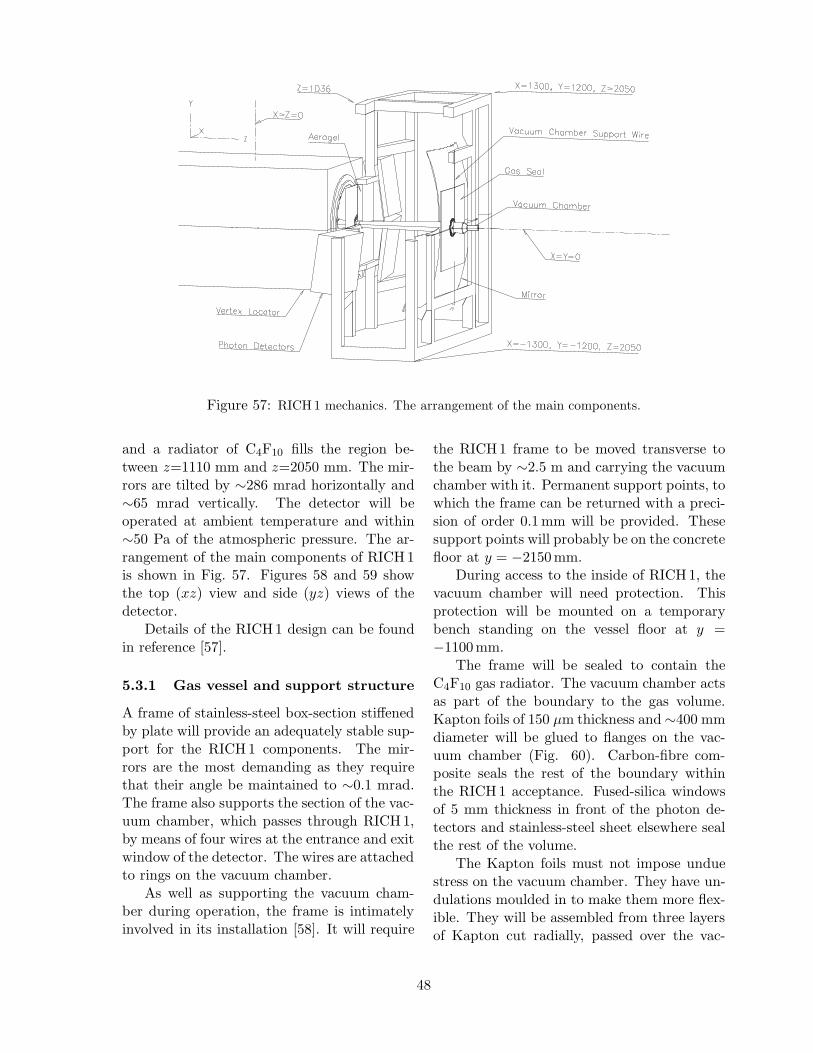
Figure 57: RICH1 mechanics. The arrangement of the main components.
and a radiator of C4F10 fills the region be-tween z=1110 mm and z=2050 mm. The mir-rors are tilted by ∼286 mrad horizontally and∼65 mrad vertically. The detector will beoperated at ambient temperature and within∼50 Pa of the atmospheric pressure. The ar-rangement of the main components of RICH1is shown in Fig. 57. Figures 58 and 59 showthe top (xz) view and side (yz) views of thedetector.
Details of the RICH1 design can be foundin reference [57].
5.3.1 Gas vessel and support structure
A frame of stainless-steel box-section stiffenedby plate will provide an adequately stable sup-port for the RICH1 components. The mir-rors are the most demanding as they requirethat their angle be maintained to ∼0.1 mrad.The frame also supports the section of the vac-uum chamber, which passes through RICH1,by means of four wires at the entrance and exitwindow of the detector. The wires are attachedto rings on the vacuum chamber.
As well as supporting the vacuum cham-ber during operation, the frame is intimatelyinvolved in its installation [58]. It will require
the RICH1 frame to be moved transverse tothe beam by ∼2.5 m and carrying the vacuumchamber with it. Permanent support points, towhich the frame can be returned with a preci-sion of order 0.1 mm will be provided. Thesesupport points will probably be on the concretefloor at y = −2150mm.
During access to the inside of RICH1, thevacuum chamber will need protection. Thisprotection will be mounted on a temporarybench standing on the vessel floor at y =−1100mm.
The frame will be sealed to contain theC4F10 gas radiator. The vacuum chamber actsas part of the boundary to the gas volume.Kapton foils of 150 µm thickness and ∼400 mmdiameter will be glued to flanges on the vac-uum chamber (Fig. 60). Carbon-fibre com-posite seals the rest of the boundary withinthe RICH1 acceptance. Fused-silica windowsof 5 mm thickness in front of the photon de-tectors and stainless-steel sheet elsewhere sealthe rest of the volume.
The Kapton foils must not impose unduestress on the vacuum chamber. They have un-dulations moulded in to make them more flex-ible. They will be assembled from three layersof Kapton cut radially, passed over the vac-
48
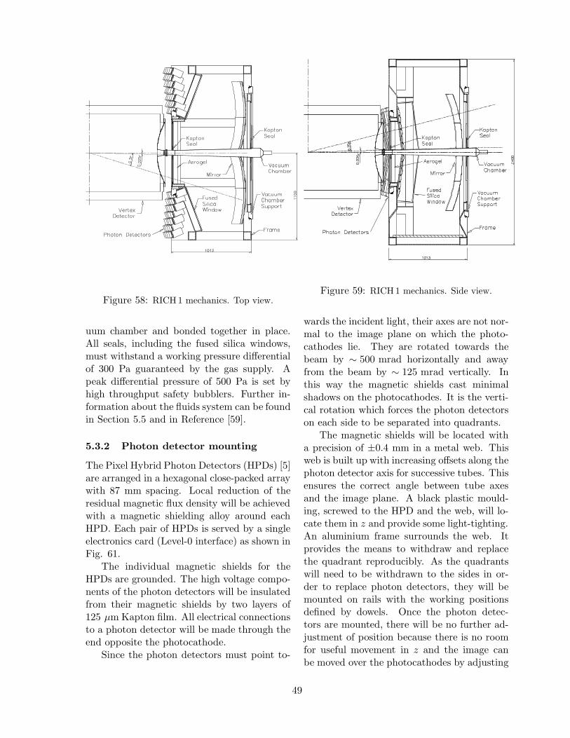
Figure 58: RICH1 mechanics. Top view.
uum chamber and bonded together in place.All seals, including the fused silica windows,must withstand a working pressure differentialof 300 Pa guaranteed by the gas supply. Apeak differential pressure of 500 Pa is set byhigh throughput safety bubblers. Further in-formation about the fluids system can be foundin Section 5.5 and in Reference [59].
5.3.2 Photon detector mounting
The Pixel Hybrid Photon Detectors (HPDs) [5]are arranged in a hexagonal close-packed arraywith 87 mm spacing. Local reduction of theresidual magnetic flux density will be achievedwith a magnetic shielding alloy around eachHPD. Each pair of HPDs is served by a singleelectronics card (Level-0 interface) as shown inFig. 61.
The individual magnetic shields for theHPDs are grounded. The high voltage compo-nents of the photon detectors will be insulatedfrom their magnetic shields by two layers of125 µm Kapton film. All electrical connectionsto a photon detector will be made through theend opposite the photocathode.
Since the photon detectors must point to-
Figure 59: RICH1 mechanics. Side view.
wards the incident light, their axes are not nor-mal to the image plane on which the photo-cathodes lie. They are rotated towards thebeam by ∼ 500 mrad horizontally and awayfrom the beam by ∼ 125 mrad vertically. Inthis way the magnetic shields cast minimalshadows on the photocathodes. It is the verti-cal rotation which forces the photon detectorson each side to be separated into quadrants.
The magnetic shields will be located witha precision of ±0.4 mm in a metal web. Thisweb is built up with increasing offsets along thephoton detector axis for successive tubes. Thisensures the correct angle between tube axesand the image plane. A black plastic mould-ing, screwed to the HPD and the web, will lo-cate them in z and provide some light-tighting.An aluminium frame surrounds the web. Itprovides the means to withdraw and replacethe quadrant reproducibly. As the quadrantswill need to be withdrawn to the sides in or-der to replace photon detectors, they will bemounted on rails with the working positionsdefined by dowels. Once the photon detec-tors are mounted, there will be no further ad-justment of position because there is no roomfor useful movement in z and the image canbe moved over the photocathodes by adjusting
49
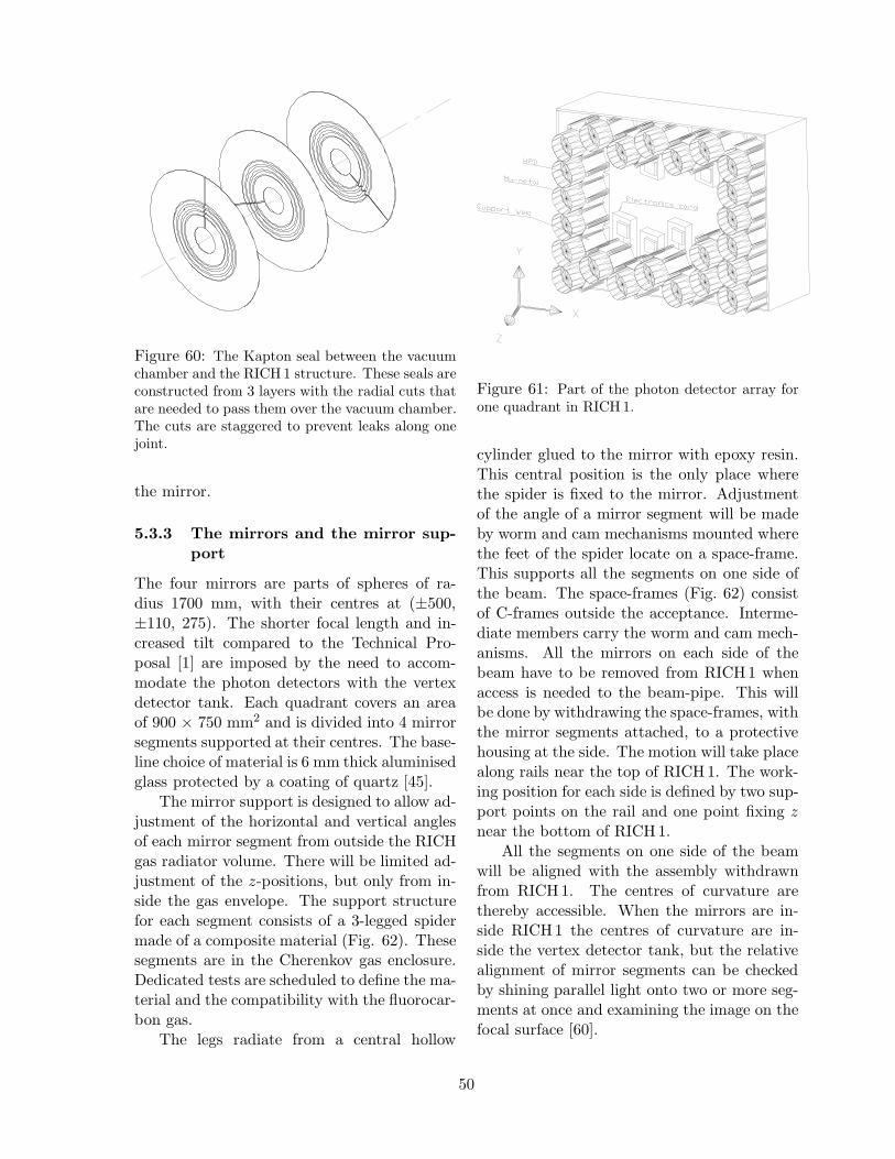
Figure 60: The Kapton seal between the vacuumchamber and the RICH1 structure. These seals areconstructed from 3 layers with the radial cuts thatare needed to pass them over the vacuum chamber.The cuts are staggered to prevent leaks along onejoint.
the mirror.
5.3.3 The mirrors and the mirror sup-port
The four mirrors are parts of spheres of ra-dius 1700 mm, with their centres at (±500,±110, 275). The shorter focal length and in-creased tilt compared to the Technical Pro-posal [1] are imposed by the need to accom-modate the photon detectors with the vertexdetector tank. Each quadrant covers an areaof 900 × 750 mm2 and is divided into 4 mirrorsegments supported at their centres. The base-line choice of material is 6 mm thick aluminisedglass protected by a coating of quartz [45].
The mirror support is designed to allow ad-justment of the horizontal and vertical anglesof each mirror segment from outside the RICHgas radiator volume. There will be limited ad-justment of the z-positions, but only from in-side the gas envelope. The support structurefor each segment consists of a 3-legged spidermade of a composite material (Fig. 62). Thesesegments are in the Cherenkov gas enclosure.Dedicated tests are scheduled to define the ma-terial and the compatibility with the fluorocar-bon gas.
The legs radiate from a central hollow
Figure 61: Part of the photon detector array forone quadrant in RICH1.
cylinder glued to the mirror with epoxy resin.This central position is the only place wherethe spider is fixed to the mirror. Adjustmentof the angle of a mirror segment will be madeby worm and cam mechanisms mounted wherethe feet of the spider locate on a space-frame.This supports all the segments on one side ofthe beam. The space-frames (Fig. 62) consistof C-frames outside the acceptance. Interme-diate members carry the worm and cam mech-anisms. All the mirrors on each side of thebeam have to be removed from RICH1 whenaccess is needed to the beam-pipe. This willbe done by withdrawing the space-frames, withthe mirror segments attached, to a protectivehousing at the side. The motion will take placealong rails near the top of RICH1. The work-ing position for each side is defined by two sup-port points on the rail and one point fixing znear the bottom of RICH1.
All the segments on one side of the beamwill be aligned with the assembly withdrawnfrom RICH1. The centres of curvature arethereby accessible. When the mirrors are in-side RICH1 the centres of curvature are in-side the vertex detector tank, but the relativealignment of mirror segments can be checkedby shining parallel light onto two or more seg-ments at once and examining the image on thefocal surface [60].
50
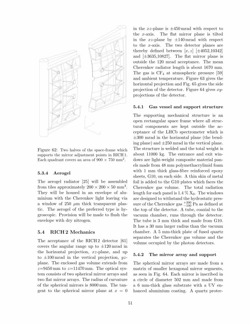
Figure 62: Two halves of the space-frame whichsupports the mirror adjustment points in RICH1.Each quadrant covers an area of 900 × 750 mm2.
5.3.4 Aerogel
The aerogel radiator [25] will be assembledfrom tiles approximately 200 × 200 × 50 mm3.They will be housed in an envelope of alu-minium with the Cherenkov light leaving viaa window of 250 µm thick transparent plas-tic. The aerogel of the preferred type is hy-groscopic. Provision will be made to flush theenvelope with dry nitrogen.
5.4 RICH2 Mechanics
The acceptance of the RICH2 detector [61]covers the angular range up to ±120 mrad inthe horizontal projection, xz-plane, and upto ±100 mrad in the vertical projection, yz-plane. The enclosed gas volume extends fromz=9450 mm to z=11470 mm. The optical sys-tem consists of two spherical mirror arrays andtwo flat mirror arrays. The radius of curvatureof the spherical mirrors is 8000 mm. The tan-gent to the spherical mirror plane at x = 0
in the xz-plane is ±450 mrad with respect tothe x-axis. The flat mirror plane is tiltedin the xz-plane by ±140 mrad with respectto the x-axis. The two detector planes arethereby defined between [x, z] [±4052,10342]and [±3635,10827]. The flat mirror plane isoutside the 120 mrad acceptance. The meanCherenkov radiator length is about 1670 mm.The gas is CF4 at atmospheric pressure [59]and ambient temperature. Figure 63 gives thehorizontal projection and Fig. 65 gives the sideprojection of the detector. Figure 64 gives xy-projections of the detector.
5.4.1 Gas vessel and support structure
The supporting mechanical structure is anopen rectangular space frame where all struc-tural components are kept outside the ac-ceptance of the LHCb spectrometer which is±300 mrad in the horizontal plane (the bend-ing plane) and ±250 mrad in the vertical plane.The structure is welded and the total weight isabout 11000 kg. The entrance and exit win-dows are light-weight composite material pan-els made from 48 mm polymethacrylimid foamwith 1 mm thick glass-fibre reinforced epoxysheets, G10, on each side. A thin skin of metalfoil is added to the G10 plates which faces theCherenkov gas volume. The total radiationlength for each panel is 1.4 % X0. The windowsare designed to withstand the hydrostatic pres-sure of the Cherenkov gas +200
−100 Pa as defined atthe top of the detector. A tube, coaxial to thevacuum chamber, runs through the detector.The tube is 3 mm thick and made from G10.It has a 30 mm larger radius than the vacuumchamber. A 5 mm-thick plate of fused quartzseparates the Cherenkov gas volume and thevolume occupied by the photon detectors.
5.4.2 The mirror array and support
The spherical mirror arrays are made from amatrix of smaller hexagonal mirror segments,as seen in Fig. 64. Each mirror is inscribed ina circle of diameter 502 mm and made froma 6 mm-thick glass substrate with a UV en-hanced aluminium coating. A quartz protec-
51
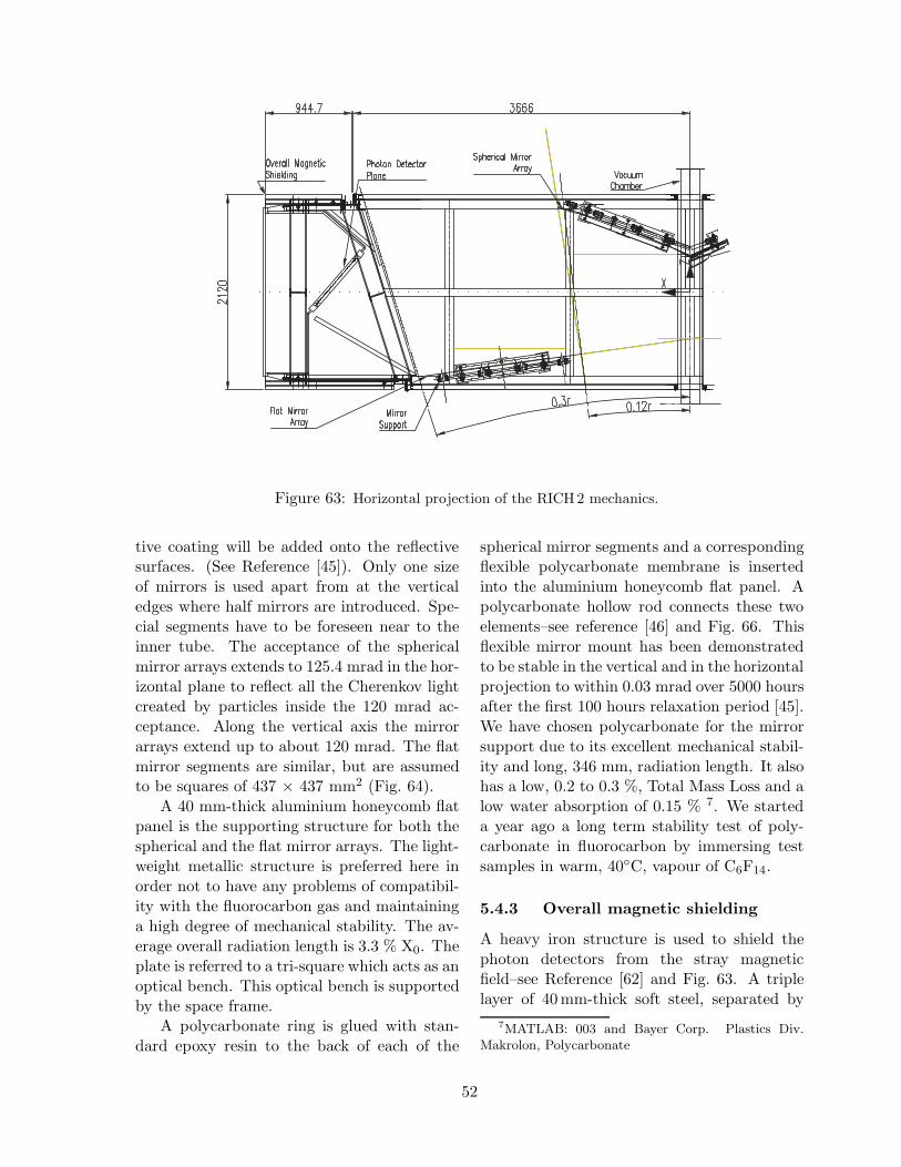
Figure 63: Horizontal projection of the RICH2 mechanics.
tive coating will be added onto the reflectivesurfaces. (See Reference [45]). Only one sizeof mirrors is used apart from at the verticaledges where half mirrors are introduced. Spe-cial segments have to be foreseen near to theinner tube. The acceptance of the sphericalmirror arrays extends to 125.4 mrad in the hor-izontal plane to reflect all the Cherenkov lightcreated by particles inside the 120 mrad ac-ceptance. Along the vertical axis the mirrorarrays extend up to about 120 mrad. The flatmirror segments are similar, but are assumedto be squares of 437 × 437 mm2 (Fig. 64).
A 40 mm-thick aluminium honeycomb flatpanel is the supporting structure for both thespherical and the flat mirror arrays. The light-weight metallic structure is preferred here inorder not to have any problems of compatibil-ity with the fluorocarbon gas and maintaininga high degree of mechanical stability. The av-erage overall radiation length is 3.3 % X0. Theplate is referred to a tri-square which acts as anoptical bench. This optical bench is supportedby the space frame.
A polycarbonate ring is glued with stan-dard epoxy resin to the back of each of the
spherical mirror segments and a correspondingflexible polycarbonate membrane is insertedinto the aluminium honeycomb flat panel. Apolycarbonate hollow rod connects these twoelements–see reference [46] and Fig. 66. Thisflexible mirror mount has been demonstratedto be stable in the vertical and in the horizontalprojection to within 0.03 mrad over 5000 hoursafter the first 100 hours relaxation period [45].We have chosen polycarbonate for the mirrorsupport due to its excellent mechanical stabil-ity and long, 346 mm, radiation length. It alsohas a low, 0.2 to 0.3 %, Total Mass Loss and alow water absorption of 0.15 % 7. We starteda year ago a long term stability test of poly-carbonate in fluorocarbon by immersing testsamples in warm, 40C, vapour of C6F14.
5.4.3 Overall magnetic shielding
A heavy iron structure is used to shield thephoton detectors from the stray magneticfield–see Reference [62] and Fig. 63. A triplelayer of 40 mm-thick soft steel, separated by
7MATLAB: 003 and Bayer Corp. Plastics Div.Makrolon, Polycarbonate
52
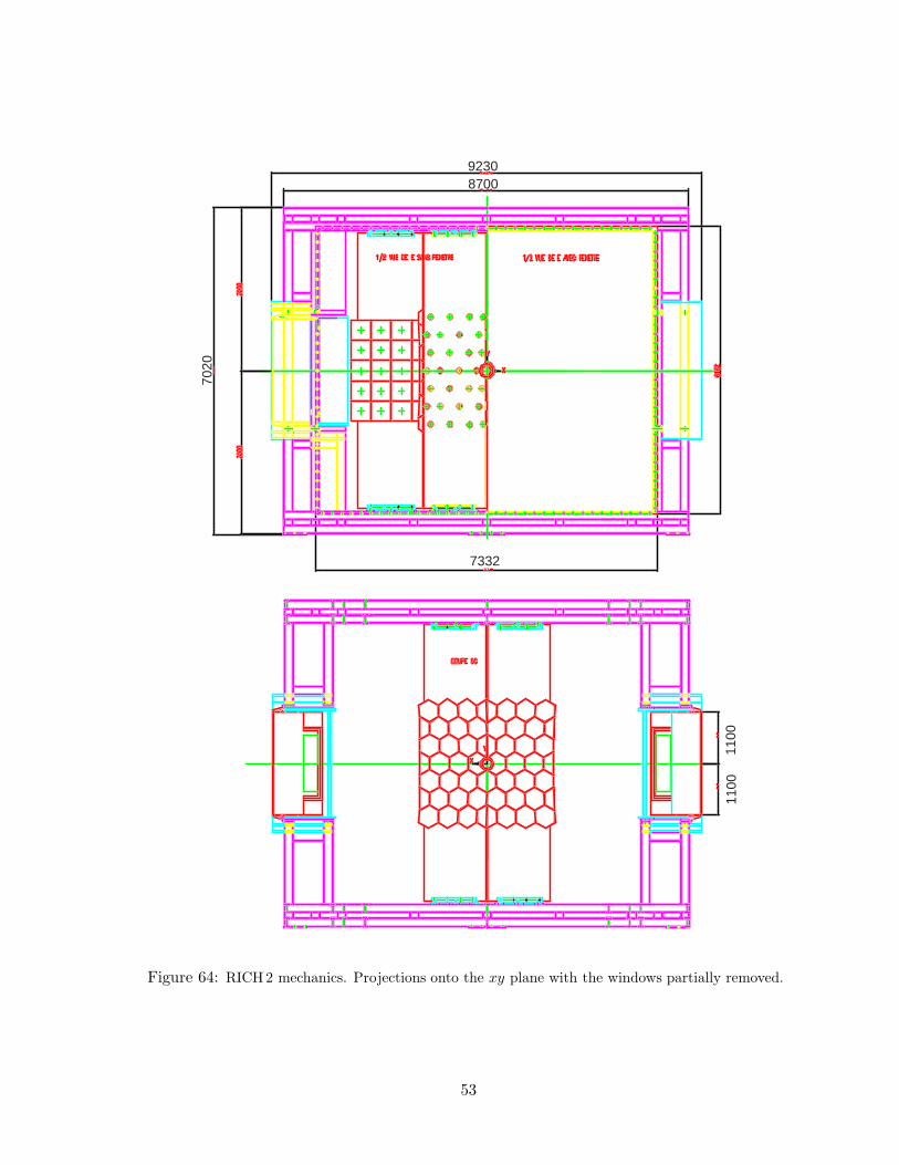
7332
92308700
7020
1100
1100
Figure 64: RICH2 mechanics. Projections onto the xy plane with the windows partially removed.
53
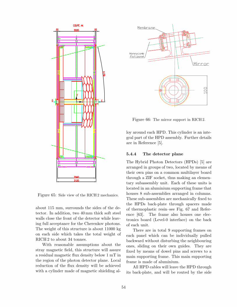
Figure 65: Side view of the RICH2 mechanics.
about 115 mm, surrounds the sides of the de-tector. In addition, two 40 mm thick soft steelwalls close the front of the detector while leav-ing full acceptance for the Cherenkov photons.The weight of this structure is about 11000 kgon each side which takes the total weight ofRICH2 to about 34 tonnes.
With reasonable assumptions about thestray magnetic field, this structure will assurea residual magnetic flux density below 1 mT inthe region of the photon detector plane. Localreduction of the flux density will be achievedwith a cylinder made of magnetic shielding al-
Figure 66: The mirror support in RICH2.
loy around each HPD. This cylinder is an inte-gral part of the HPD assembly. Further detailsare in Reference [5].
5.4.4 The detector plane
The Hybrid Photon Detectors (HPDs) [5] arearranged in groups of two, located by means oftheir own pins on a common multilayer boardthrough a ZIF socket, thus making an elemen-tary subassembly unit. Each of these units islocated in an aluminium supporting frame thathouses 8 sub-assemblies arranged in columns.These sub-assemblies are mechanically fixed tothe HPDs back-plate through spacers madeof thermoplastic resin–see Fig. 67 and Refer-ence [63]. The frame also houses one elec-tronics board (Level-0 interface) on the backof each unit.
There are in total 9 supporting frames oneach panel which can be individually pulledbackward without disturbing the neighbouringones, sliding on their own guides. They arefixed by means of dowel pins and screws to amain supporting frame. This main supportingframe is made of aluminium.
All HPD cables will leave the HPD throughits back-plate, and will be routed by the side
54
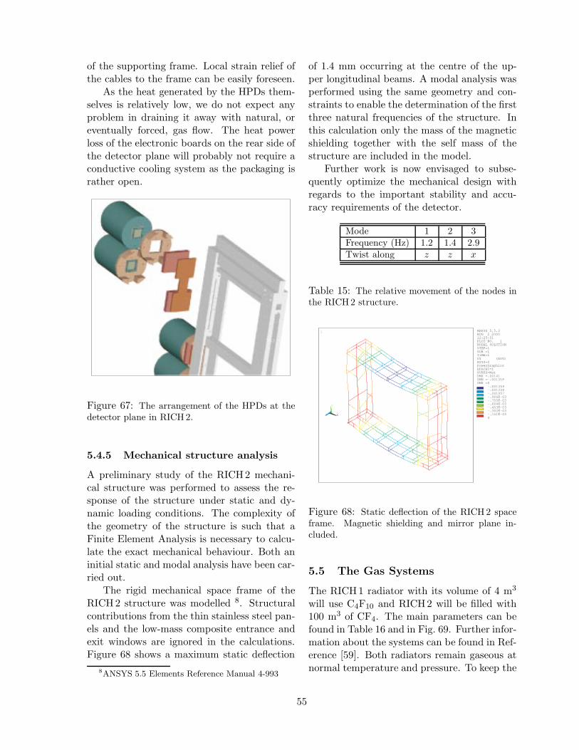
of the supporting frame. Local strain relief ofthe cables to the frame can be easily foreseen.
As the heat generated by the HPDs them-selves is relatively low, we do not expect anyproblem in draining it away with natural, oreventually forced, gas flow. The heat powerloss of the electronic boards on the rear side ofthe detector plane will probably not require aconductive cooling system as the packaging israther open.
Figure 67: The arrangement of the HPDs at thedetector plane in RICH2.
5.4.5 Mechanical structure analysis
A preliminary study of the RICH2 mechani-cal structure was performed to assess the re-sponse of the structure under static and dy-namic loading conditions. The complexity ofthe geometry of the structure is such that aFinite Element Analysis is necessary to calcu-late the exact mechanical behaviour. Both aninitial static and modal analysis have been car-ried out.
The rigid mechanical space frame of theRICH2 structure was modelled 8. Structuralcontributions from the thin stainless steel pan-els and the low-mass composite entrance andexit windows are ignored in the calculations.Figure 68 shows a maximum static deflection
8ANSYS 5.5 Elements Reference Manual 4-993
of 1.4 mm occurring at the centre of the up-per longitudinal beams. A modal analysis wasperformed using the same geometry and con-straints to enable the determination of the firstthree natural frequencies of the structure. Inthis calculation only the mass of the magneticshielding together with the self mass of thestructure are included in the model.
Further work is now envisaged to subse-quently optimize the mechanical design withregards to the important stability and accu-racy requirements of the detector.
Mode 1 2 3Frequency (Hz) 1.2 1.4 2.9Twist along z z x
Table 15: The relative movement of the nodes inthe RICH2 structure.
ANSYS 5.5.3AUG 2 200012:25:01PLOT NO. 1NODAL SOLUTIONSTEP=1SUB =1TIME=1UY (AVG)RSYS=0PowerGraphicsEFACET=1AVRES=MatDMX =.00141SMN =-.001359SMX =0
1
MN
MX
X
Y
Z
-.001359-.001208-.001057-.906E-03-.755E-03-.604E-03-.453E-03-.302E-03-.151E-030
Figure 68: Static deflection of the RICH2 spaceframe. Magnetic shielding and mirror plane in-cluded.
5.5 The Gas Systems
The RICH1 radiator with its volume of 4 m3
will use C4F10 and RICH2 will be filled with100 m3 of CF4. The main parameters can befound in Table 16 and in Fig. 69. Further infor-mation about the systems can be found in Ref-erence [59]. Both radiators remain gaseous atnormal temperature and pressure. To keep the
55
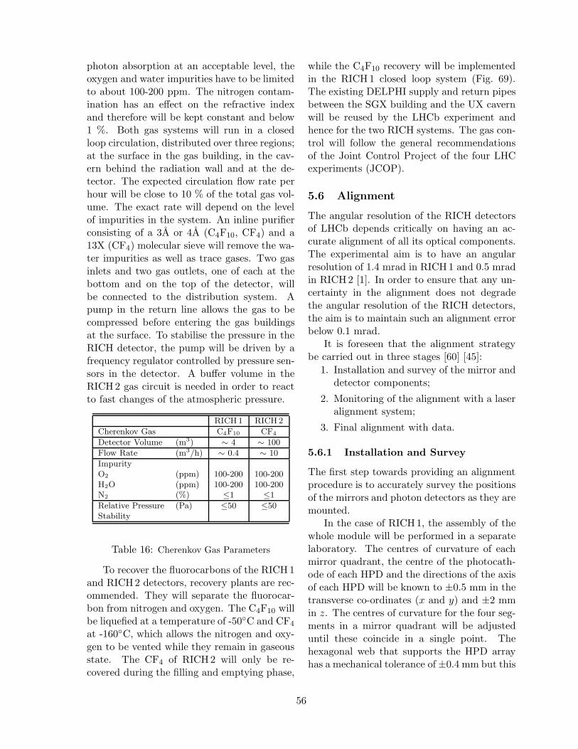
photon absorption at an acceptable level, theoxygen and water impurities have to be limitedto about 100-200 ppm. The nitrogen contam-ination has an effect on the refractive indexand therefore will be kept constant and below1 %. Both gas systems will run in a closedloop circulation, distributed over three regions;at the surface in the gas building, in the cav-ern behind the radiation wall and at the de-tector. The expected circulation flow rate perhour will be close to 10 % of the total gas vol-ume. The exact rate will depend on the levelof impurities in the system. An inline purifierconsisting of a 3A or 4A (C4F10, CF4) and a13X (CF4) molecular sieve will remove the wa-ter impurities as well as trace gases. Two gasinlets and two gas outlets, one of each at thebottom and on the top of the detector, willbe connected to the distribution system. Apump in the return line allows the gas to becompressed before entering the gas buildingsat the surface. To stabilise the pressure in theRICH detector, the pump will be driven by afrequency regulator controlled by pressure sen-sors in the detector. A buffer volume in theRICH2 gas circuit is needed in order to reactto fast changes of the atmospheric pressure.
RICH1 RICH 2
Cherenkov Gas C4F10 CF4
Detector Volume (m3) ∼ 4 ∼ 100
Flow Rate (m3/h) ∼ 0.4 ∼ 10
ImpurityO2 (ppm) 100-200 100-200H2O (ppm) 100-200 100-200N2 (%) ≤1 ≤1
Relative Pressure (Pa) ≤50 ≤50Stability
Table 16: Cherenkov Gas Parameters
To recover the fluorocarbons of the RICH1and RICH2 detectors, recovery plants are rec-ommended. They will separate the fluorocar-bon from nitrogen and oxygen. The C4F10 willbe liquefied at a temperature of -50C and CF4
at -160C, which allows the nitrogen and oxy-gen to be vented while they remain in gaseousstate. The CF4 of RICH2 will only be re-covered during the filling and emptying phase,
while the C4F10 recovery will be implementedin the RICH1 closed loop system (Fig. 69).The existing DELPHI supply and return pipesbetween the SGX building and the UX cavernwill be reused by the LHCb experiment andhence for the two RICH systems. The gas con-trol will follow the general recommendationsof the Joint Control Project of the four LHCexperiments (JCOP).
5.6 Alignment
The angular resolution of the RICH detectorsof LHCb depends critically on having an ac-curate alignment of all its optical components.The experimental aim is to have an angularresolution of 1.4 mrad in RICH1 and 0.5 mradin RICH2 [1]. In order to ensure that any un-certainty in the alignment does not degradethe angular resolution of the RICH detectors,the aim is to maintain such an alignment errorbelow 0.1 mrad.
It is foreseen that the alignment strategybe carried out in three stages [60] [45]:
1. Installation and survey of the mirror anddetector components;
2. Monitoring of the alignment with a laseralignment system;
3. Final alignment with data.
5.6.1 Installation and Survey
The first step towards providing an alignmentprocedure is to accurately survey the positionsof the mirrors and photon detectors as they aremounted.
In the case of RICH1, the assembly of thewhole module will be performed in a separatelaboratory. The centres of curvature of eachmirror quadrant, the centre of the photocath-ode of each HPD and the directions of the axisof each HPD will be known to ±0.5 mm in thetransverse co-ordinates (x and y) and ±2 mmin z. The centres of curvature for the four seg-ments in a mirror quadrant will be adjusteduntil these coincide in a single point. Thehexagonal web that supports the HPD arrayhas a mechanical tolerance of ±0.4 mm but this
56
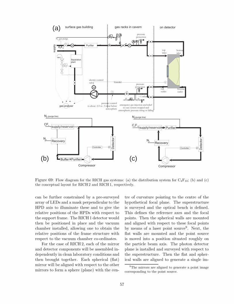
(a)
(b) (c)
Figure 69: Flow diagram for the RICH gas systems: (a) the distribution system for C4F10; (b) and (c)the conceptual layout for RICH2 and RICH1, respectively.
can be further constrained by a pre-surveyedarray of LEDs and a mask perpendicular to theHPD axis to illuminate these and to give therelative positions of the HPDs with respect tothe support frame. The RICH1 detector wouldthen be positioned in place and the vacuumchamber installed, allowing one to obtain therelative positions of the frame structure withrespect to the vacuum chamber co-ordinates.
For the case of RICH2, each of the mirrorand detector components will be assembled in-dependently in clean laboratory conditions andthen brought together. Each spherical (flat)mirror will be aligned with respect to the othermirrors to form a sphere (plane) with the cen-
tre of curvature pointing to the centre of thehypothetical focal plane. The superstructureis surveyed and the optical bench is defined.This defines the reference axes and the focalpoints. Then the spherical walls are mountedand aligned with respect to these focal pointsby means of a laser point source9. Next, theflat walls are mounted and the point sourceis moved into a position situated roughly onthe particle beam axis. The photon detectorplane is installed and surveyed with respect tothe superstructure. Then the flat and spher-ical walls are aligned to generate a single im-
9The mirrors are aligned to generate a point imagecorresponding to the point source.
57
age point on the normal to the photodetectorplane. When the RICH2 detector is lowered inthe pit and placed on the beam axis, the rel-ative alignment of the flat and spherical wallsis repeated to check and correct eventual mis-alignments. The overall alignment error fore-seen is set solely by the survey (±1 mm shift onthe photodetector plane) and by the precisionof the optical mounts. The resolution for thespherical and the flat mirrors and the mountprecision will set the overall resolution of theoptical system. At the photocathode plane, itcan be expressed as√∑
i σ2i × l2i
where li is the path length of the light to thephotocathode and i denotes the different com-ponents; spherical/flat mirror and the mirrormounts. For equal error on all the componentsand an overall error σ ≤ 0.1 mrad gives σi ≤0.06 mrad.
5.6.2 Laser Alignment System
A laser alignment system for each of the twoRICH detectors can perform the following twofunctions:
1. It can perform a quick and final cross-check of the link between the mirrorplanes and the photon detector plane be-fore any gas is introduced into the gasenclosure.
2. It can be used to continue monitoringthe positions of the detector componentsthroughout data taking, thereby makingallowances for thermal and vibrationalcorrections.
The laser alignment system would consistof a series of discrete laser points installed infront of the first mirror plane (at least twopoints per mirror) that can be compared withtheir theoretically mapped positions on thephoton detector plane. The unambiguous na-ture of the laser points simplifies the alignmentprocedure, allowing one to optimise the tiltsand positions of the mirrors in real time. Thedelivery system for these laser beams could
be an array of single-mode optical fibres withcollimator optics, producing diffraction limitedGaussian shaped laser beams. These have beenproposed for the multi-point alignment systemof the ATLAS muon spectrometer [64, 65, 66]producing beams with a width of 2-3 mm overdistances between 10-20 m [64]. These fibreswith their collimating optics could be arrangedin a matrix, supported by a light frame struc-ture, in front of the spherical mirrors, onlyadding minimally to the material budget insidethe acceptance of the RICH detectors. The fi-bres could be mounted on the spherical mir-rors themselves, perpendicular to the mirrorsurface. This would avoid having a supportstructure. Alternatively a laser system with apiezo-assisted mirror can scan the whole mir-ror array onto the photodetectors. The aimis for an initial alignment precision of about0.5 mrad. Further discussion on these systemsis given in Reference [60].
5.6.3 Alignment with data
The final stage in the alignment process wouldinvolve performing an iterative alignment pro-cedure with the data themselves, by selectingtracks with β ∼= 1, and minimising the resid-uals incurred by tilt and position adjustmentswith respect to the theoretically expected po-sitions of Cherenkov photons unambiguouslyassociated to mirror segments, if the mirrorsand detectors were ideally aligned [67, 68].
If the reconstructed Cherenkov angle is θrec
and the expected angle is θexp, any misalign-ment in the mirror segments with respect tothe photon detectors is observed by measuringthe difference between the two angles as a func-tion of the reconstructed azimuthal Cherenkovangle φrec:
θrec − θexp = A cos(φrec − φ0), (4)
where A and φ0 are fit parameters.The positions and tilt angles of the mirror
segments are displaced in such a manner thatthe Cherenkov angle residuals are minimised.This procedure has to be iterated a numberof times to achieve the optimal residuals in all
58

the mirror segments. A preliminary study per-formed within the context of RICH2 [68], sug-gests that if the initial alignment has an ac-curacy of ∼ 0.5 mrad, then a total alignmentaccuracy of 0.2 mrad (including mirror qual-ity) can be achieved.
5.7 Monitoring and Control
The performance of the RICH detectors ofLHCb can be kept under control if one isable to monitor physically relevant quanti-ties throughout the duration of the experi-ment [60]. The main factors that affect theperformance are the conditions of the gas, in-cluding its refractive index and transmissioncharacteristics, the stability of the supportstructures, the functionality of the electronicsand the efficiency and quality of the photondetectors.
Each of the closed circuit re-circulation gassystems for the two RICH detectors [59] in-clude control and monitoring systems to en-sure the quality of the two gases, C4F10 andCF4. The following parameters will need to bemonitored in the re-circulation plants:
1. Flow meters to measure the gas flow;
2. Pressure sensors for atmospheric pres-sure and for pressure differentials be-tween gas inlet and outlet;
3. Gas purity analysers, to measure theconcentration of water and oxygen (to re-main below 100-200 ppm);
4. Temperature sensors in the gas vessel;
5. The temperature, pressure and valvecontrols of the cryogenic plant;
6. The nitrogen concentration in the gas(which should be constant ≤ 1 %) bymeans of an ultrasonic sensor to measurethe velocity of sound [69];
7. The refractive index of the gas as afunction of pressure with a Fabry-Perotinterferometer [70, 71] consisting of a
monochromator, etalon and CCD cam-era10;
8. The transparency and attenuation lengthof the gas between 200 and 800 nm with amonochromator and a gas vessel of vary-ing length [72].
The mechanical stability of the support-ing frame needs to be monitored to ensurethat thermal and vibrational movements donot affect the position resolution of the mir-ror mounts and the photon detector mounts.Semi-transparent position sensitive amorphoussilicon sensors [64, 65, 66], developed for theoptical multi-point alignment system of theATLAS muon spectrometer, can be deployedon the mechanical frames. Deflections in thesupporting structures are measured by align-ment reference points delivered by lasers at-tached to single-mode fibres with collimatingoptics. The sensors consist of two 20×20 mm2
orthogonal layers of 64 strips that can achievea spatial resolution of ∼ 1 µm [64, 73].
The following detector electronics parame-ters will need to be measured and controlled:
1. High voltage of the photon detectortubes;
2. Voltage across the HPD focusing ele-ments;
3. Bias voltage for the pixel detector;
4. Leakage current of the pixel detectors;
5. Low voltage for the detector electronics;
6. Binary electronics discriminator thresh-old;
7. Test pulse for electronics calibration.
The identification of dead channels and themeasurement of photon detector efficienciescan be performed with a diffuse pulsed light
10One would compare to the average n obtained fromthe reconstruction of the Cherenkov angle.
59
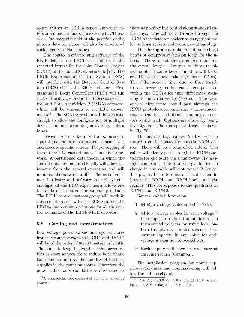
source (either an LED, a xenon lamp with fil-ters or a monochromator) inside the RICH ves-sels. The magnetic field at the position of thephoton detector plane will also be monitoredwith a series of Hall probes.
The control hardware and software of theRICH detectors of LHCb will conform to theaccepted format for the Joint Control Project(JCOP) of the four LHC experiments [74]. TheLHCb Experimental Control System (ECS)will interface with the Detector Control Sys-tem (DCS) of the the RICH detectors. Pro-grammable Logic Controllers (PLC) will runeach of the devices under the Supervisory Con-trol and Data Acquisition (SCADA) software,which will be common to all LHC experi-ments11. The SCADA system will be versatileenough to allow the configuration of multipledevice components running on a variety of databuses.
Device user interfaces will allow users tocontrol and monitor parameters, alarm levelsand execute specific actions. Proper logging ofthe data will be carried out within this frame-work. A partitioned data model in which thecontrol units are mounted locally will allow au-tonomy from the general operation and willminimise the network traffic. The use of com-mon hardware and software control systemsamongst all the LHC experiments allows oneto standardise solutions for common problems.The RICH control systems group will work inclose collaboration with the ECS group of theLHC to find common solutions for all the con-trol demands of the LHCb RICH detectors.
5.8 Cabling and Infrastructure
Low voltage power cables and optical fibresfrom the counting room to RICH1 and RICH2will be of the order of 80-100 metres in length.The aim is to keep the lengths of the power ca-bles as short as possible to reduce both ohmiclosses and to improve the stability of the basesupplies in the counting rooms. Therefore thepower cable route should be as direct and as
11A commercial tool contracted out by a tenderingprocess.
short as possible but routed along standard ca-ble trays. The cables will route through theRICH photodetector enclosure using standardlow voltage sockets and panel mounting plugs.
The fibre optic route should not incur sharpbends or compressive/tension loads for the fi-bres. There is not the same restriction onthe overall length. Lengths of fibres termi-nating at the same Level-1 module will be ofequal lengths to better than 1/6 metre (0.5 ns).The differences in time due to fibre lengthto each receiving module can be compensatedwithin the TTCrx for time differences span-ning 16 bunch crossings (400 ns). The idealoptical fibre route should pass through theRICH photodetector enclosure without incur-ring a penalty of additional coupling connec-tors at the wall. Options are currently beinginvestigated. The conceptual design is shownin Fig. 70.
The high voltage cables, 20 kV, will berouted from the control room to the RICH ves-sels. There will be a total of 64 cables. Thecables will ideally pass through the RICH pho-todetector enclosure via a multi-way HV gas-tight connector. The total energy due to thecharge in any cable will not exceed 2 Joules.The proposal is to terminate the cables and fi-bres at the RICH1 and RICH2 areas at eightregions. This corresponds to the quadrants inRICH1 and RICH2.
General cable information:
1. 64 high voltage cables carrying 20 kV.
2. 64 low voltage cables for each voltage12
It is hoped to reduce the number of thetransmitted voltages by using local on-board regulators. In this scheme, totalcurrent capacity in any cable for eachvoltage is seen not to exceed 5 A.
3. Each supply will have its own currentcarrying return (Common).
The installation program for power sup-plies/racks/links and commissioning will fol-low the LHCb schedule.
12+5 V; 3.3 V; 2.0 V; +1.6 V digital; +1.6 V ana-logue; +0.8 V analogue; +0.8 V digital.
60
Figure 70: Layout of the LHCb experiment showing the detectors, the counting rooms and the cablerouting. RICH electronics racks are located in the counting rooms.
The common point for the low voltage andthe high voltage will be at the detector end.Care will be taken to ensure that if any breakor open connection occurs in these cables orlinks the high and low voltages do not drift todangerous levels. Where necessary, earthingstandards, currently being studied by LHCb,will be adhered to.
5.9 Safety aspects
The RICH detectors of LHCb will follow theCERN safety rules and codes, CERN safetydocument SAPOCO 42 and European and/orinternational construction codes for structuralengineering as described in EUROCODE 3.
Specific risks, and actions, as discussed inthe Initial Safety Discussion (ISD) with theCERN Technical Inspection and Safety (TIS)Commission:
1. The Cherenkov gases, C4F10 (CAS-RN355-25-9) and CF4 (CAS-RN 75-73-0),are not flammable and have UN classifi-cation 2.2 13. Due to the relatively large
13UN classification 2.2 corresponds to non-toxic andnon-flammable substances.
quantities of these gases in the cavern,4 m3 of C4F10 and 100 m3 of CF4, andthe high density of these gases, 10.5 g/lfor C4F10 and 3.9 g/l for CF4, oxygen de-ficiency meters will be installed near tothe detectors.
2. As the detectors will be operated witha maximum overpressure towards the at-mosphere of 500 Pa set by high through-put bubblers, the vessels are not classi-fied as pressure vessels 14.
3. The quartz plates, which isolate thephoton detector environment from theCherenkov gas, will be tested 15.
4. Particular attention will be given to theWelding Procedure Specification both forthe aluminium and for the stainless steeland to the inspection of these welds.
5. The photon detectors will be run at20 kV 16. The total current for each sup-ply line will be ≤ 100µA. The low volt-
14Safety code D2 Rev.215Safety Instructions 3416H.V.A. as defined in Safety Instructions 33
61

age supply to the detector read-out is be-low 15 V 17. The total power dissipationon the detectors is ≤ 1kW and ≤ 8kW inthe counting rooms in the cavern. Ap-propriate interlocks and current moni-tors will be installed together with inter-rupts at the source.
6. Work will occasionally be done inside thegas enclosure of the detector. Appropri-ate purge of the fluorocarbons and ven-tilation will be ensured 18.
7. The high pressure part of the gas sys-tems is located in the surface buildings.The systems will be built according tothe appropriate rules 19.
8. The effects of Seismic activity will bestudied in collaboration with TIS.
17Safe Extra Low Voltage (S.E.L.V.) as defined inSafety Instructions 33
18Safety Code A4 Rev19Safety Instruction 42 and Safety Code D2 Rev.2
62
6 Project Organisation
6.1 Schedule
The overall work programme and schedule issummarized in Fig. 71. It covers the period upto mid 2005, the time at which LHC collisionsare anticipated. The schedule is planned toensure that the RICH detectors are fully com-missioned and operating together with otherLHCb sub-detectors by this time.
A critical task is the production of the HPDphoton detectors. The manufacturer (DEP)has proposed a production rate of 20 HPDs permonth. Before this production can commencethe anode assembly, including the pixel read-out chip must be available for encapsulation inthe HPD. In the event of a delay in the read-out development DEP could increase the pro-duction rate to 30 tubes per month, but thiscontingency would require an additional fabri-cation plant with consequent increase of 3% onthe HPD price. The schedule for the backupMAPMT technology, given in Appendix A,also ensures that the RICH detectors will beready by mid-2005. This is possible due to thefact that the readout electronics is external tothe tube, so its production and testing can becarried out in parallel with tube manufacture.
6.1.1 Completion of R&D
Several of the tasks included in the schedulewill involve further R&D before production.
1. The pixel chip: the current ALICE-LHCb iteration of this chip will be deliv-ered in September 2000. Following test-ing it will be bump-bonded to the sili-con sensor then encapsulated and testedin an HPD. Design of the final chip willcontinue during 2000 and testing will becompleted in 2001.
2. Readout electronics: Prototypes of theLevel-0 adaptor board, the optical linksand the Level-1 readout board will beproduced during 2000 to verify the com-plete binary readout chain.
3. Engineering design: the design of theRICH vessels, support structure, mir-rors and their adjustable mounting sys-tem will be reviewed and, in the case ofthe optical components, undergo furthertesting before finalizing detailed draw-ings by end 2001.
4. Aerogel: large tiles with high clarity willenhance the low-energy particle identifi-cation performance. An ongoing R&Dprogramme testing high clarity samplesproduced at Novosibirsk will continueduring three further years.
5. Alignment, monitoring and control: dif-ferent options are proposed to fulfil thevarious tasks in this category, and pro-totyping and testing will continue beforethe final technique is chosen before end2001.
6.1.2 Construction
The major construction tasks include:
1. RICH vessels, superstructure, optics andphoton detector mounting: require a pro-duction time of approximately one year,and will be completed during 2003. Theproduction time of the largest compo-nent, the RICH2 vessel and support, hasbeen estimated at 10 months by a com-mercial engineering company.
2. Photodetectors: the rate of productionproposed by DEP is 20/month, thus twoyears are needed. Years 2002 and 2003are foreseen in the schedule.
3. Readout electronics: the pixel chip pro-duction is scheduled during 2001, intime for encapsulation in the produc-tion HPDs. Production of the read-out electronics chain (from HPD pin-outto DAQ) is scheduled to be completedby end 2003. The only LHCb-specificelectronics components are the radiation-hard chips required for the Level-0 inter-face board. These involve common LHC
63
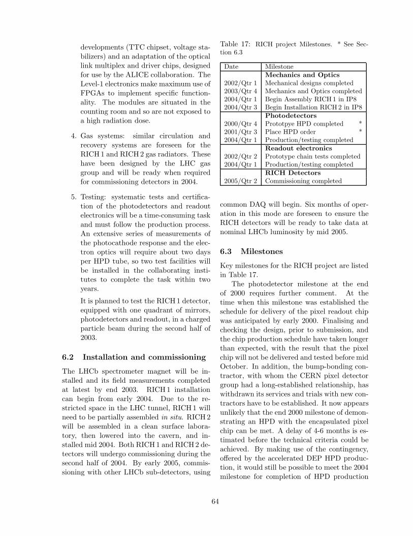
developments (TTC chipset, voltage sta-bilizers) and an adaptation of the opticallink multiplex and driver chips, designedfor use by the ALICE collaboration. TheLevel-1 electronics make maximum use ofFPGAs to implement specific function-ality. The modules are situated in thecounting room and so are not exposed toa high radiation dose.
4. Gas systems: similar circulation andrecovery systems are foreseen for theRICH1 and RICH2 gas radiators. Thesehave been designed by the LHC gasgroup and will be ready when requiredfor commissioning detectors in 2004.
5. Testing: systematic tests and certifica-tion of the photodetectors and readoutelectronics will be a time-consuming taskand must follow the production process.An extensive series of measurements ofthe photocathode response and the elec-tron optics will require about two daysper HPD tube, so two test facilities willbe installed in the collaborating insti-tutes to complete the task within twoyears.
It is planned to test the RICH1 detector,equipped with one quadrant of mirrors,photodetectors and readout, in a chargedparticle beam during the second half of2003.
6.2 Installation and commissioning
The LHCb spectrometer magnet will be in-stalled and its field measurements completedat latest by end 2003. RICH1 installationcan begin from early 2004. Due to the re-stricted space in the LHC tunnel, RICH1 willneed to be partially assembled in situ. RICH2will be assembled in a clean surface labora-tory, then lowered into the cavern, and in-stalled mid 2004. Both RICH1 and RICH2 de-tectors will undergo commissioning during thesecond half of 2004. By early 2005, commis-sioning with other LHCb sub-detectors, using
Table 17: RICH project Milestones. * See Sec-tion 6.3
Date MilestoneMechanics and Optics
2002/Qtr 1 Mechanical designs completed2003/Qtr 4 Mechanics and Optics completed2004/Qtr 1 Begin Assembly RICH1 in IP82004/Qtr 3 Begin Installation RICH 2 in IP8
Photodetectors2000/Qtr 4 Prototpye HPD completed *2001/Qtr 3 Place HPD order *2004/Qtr 1 Production/testing completed
Readout electronics2002/Qtr 2 Prototype chain tests completed2004/Qtr 1 Production/testing completed
RICH Detectors2005/Qtr 2 Commissioning completed
common DAQ will begin. Six months of oper-ation in this mode are foreseen to ensure theRICH detectors will be ready to take data atnominal LHCb luminosity by mid 2005.
6.3 Milestones
Key milestones for the RICH project are listedin Table 17.
The photodetector milestone at the endof 2000 requires further comment. At thetime when this milestone was established theschedule for delivery of the pixel readout chipwas anticipated by early 2000. Finalising andchecking the design, prior to submission, andthe chip production schedule have taken longerthan expected, with the result that the pixelchip will not be delivered and tested before midOctober. In addition, the bump-bonding con-tractor, with whom the CERN pixel detectorgroup had a long-established relationship, haswithdrawn its services and trials with new con-tractors have to be established. It now appearsunlikely that the end 2000 milestone of demon-strating an HPD with the encapsulated pixelchip can be met. A delay of 4-6 months is es-timated before the technical criteria could beachieved. By making use of the contingency,offered by the accelerated DEP HPD produc-tion, it would still be possible to meet the 2004milestone for completion of HPD production
64
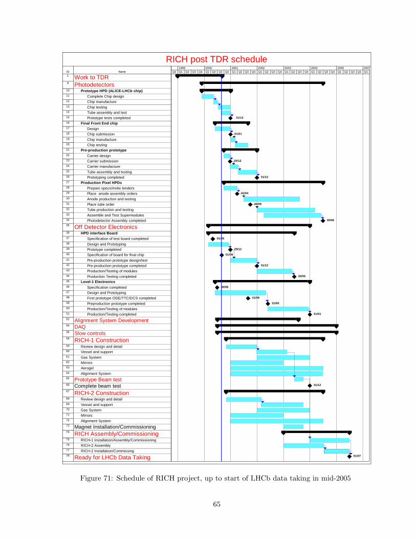
ID Name1 Work to TDR9 Photodetectors
10 Prototype HPD (ALICE-LHCb chip)11 Complete Chip design12 Chip manufacture13 Chip testing14 Tube assembly and test15 Prototype tests completed16 Final Front End chip17 Design18 Chip submission19 Chip manufacture20 Chip testing21 Pre-production prototype22 Carrier design23 Carrier submission24 Carrier manufacture25 Tube assembly and testing26 Prototyping completed27 Production Pixel HPDs28 Prepare specs/invite tenders29 Place anode assembly orders30 Anode production and testing31 Place tube order32 Tube production and testing33 Assemble and Test Supermodules34 Photodetector Assembly completed35 Off Detector Electronics36 HPD interface Board37 Specification of test board completed38 Design and Prototyping39 Prototype completed40 Specification of board for final chip41 Pre-production prototype design/test42 Pre-production prototype completed43 Production/Testing of modules44 Production Testing completed45 Level-1 Electronics46 Specification completed47 Design and Prototyping48 First prototype ODE/TTC/DCS completed49 Preproduction prototype completed50 Production/Testing of modules51 Production/Testing completed52 Alignment System Development54 DAQ56 Slow controls58 RICH-1 Construction59 Review design and detail60 Vessel and support61 Gas System62 Mirrors63 Aerogel64 Alignment System65 Prototype Beam test66 Complete beam test67 RICH-2 Construction68 Review design and detail69 Vessel and support70 Gas System71 Mirrors72 Alignment System73 Magnet Installation/Commissioning74 RICH Assembly/Commissioning75 RICH-1 Installation/Assembly/Commissioning76 RICH-2 Assembly77 RICH-2 Installation/Commissing78 Ready for LHCb Data Taking
31/12
01/01
25/12
31/12
01/04
30/09
30/06
01/05
29/12
01/09
31/12
30/05
30/06
31/08
31/05
01/01
31/12
01/07
Q4 Q1 Q2 Q3 Q4 Q1 Q2 Q3 Q4 Q1 Q2 Q3 Q4 Q1 Q2 Q3 Q4 Q1 Q2 Q3 Q4 Q1 Q2 Q3 Q4 Q1 Q2 Q3 Q4 Q11999 2000 2001 2002 2003 2004 2005 200
RICH post TDR schedule
Figure 71: Schedule of RICH project, up to start of LHCb data taking in mid-2005
65
and testing. The situation will be reviewed atthe end 2000 milestone date, when more in-formation on the status of the pixel chip andon the bump-bonding process will be available.Options to be considered at this time would in-clude pursuing the HPD, with a revised sched-ule, or changing over to the backup MAPMTtechnology.
6.4 Costs
The total cost for the RICH detector system isestimated to be 7677 kCHF. Costs are shownin Tables 18 and 19, separately for RICH1 andRICH2. Where appropriate, spares have beenincluded. More than 70% of the total cost es-timate is based on quotes from industry or re-cent purchases of similar items (e.g. mirrorsand quartz plates by the COMPASS collabo-ration).
6.5 Division of responsibilities
Institutes currently working on the LHCbRICH project are: CERN, Universities of Bris-tol, Cambridge, Genova, Glasgow, Edinburgh,Milano, Oxford, Imperial College (London)and the Rutherford Appleton Laboratory.
The sharing of responsibilities for the mainRICH project tasks is listed in Table 20. Itis not exhaustive, nor exclusive. For exam-ple software is clearly a major task, where it isunderstood that the RICH group is responsibleand will have the resources (8 FTE) to provideall RICH specific software, for DAQ, monitor-ing, reconstruction, pattern recognition, andLevel-3 trigger algorithms. The responsibili-ties for the MAPMT as specified in the Ta-ble are limited to maintaining its viability as abackup, until the HPD satisfies the milestones.
66

Table 18: RICH1 project costs (kCHF).
Item Unit Number sub-totalof units (kCHF)
Mechanics: 629Vessel superstructure m3 5Spherical mirror m2 3Mirror support structure module 1Photodetector support module 4Quartz window m2 1.5Aerogel litre 50
Photodetectors: 1473Vacuum tube piece 184Ceramic carrier piece 184Silicon sensor piece 184F/E chip piece 184Anode assembly (incl bump bond) piece 184Silicon bias supply module 28HV supply module 28
Electronics: 537Adapter board board 92L0-Trigger/clock links link 92L0-L1 data links link 368L0 reference module module 2L1 boards board 23L1-Trigger/clock links link 23L1-RU data links link 23Readout Units module 7Crates crate 2power supplies/cables piece 28
Services: 365Freezer module 1Compressor module 1Storage tank module 1Tubing, instr/high pressure system 1Tubing, instr/low pressure system 1Programmable controllers system 1Optical alignment system system 1Gas system monitoring system 1Refractive index monitoring system 1
RICH1 TOTAL 3004
67

Table 19: RICH2 project costs (kCHF).
Item Unit Number sub-totalof units (kCHF)
Mechanics: 1204Vessel superstructure m3 100Spherical mirror m2 9.2Plane mirror m2 7.6Mirror support structure module 4Photodetector support module 2Quartz window m2 2Magnetic shielding tonne 22
Photodetectors: 2290Vacuum tube piece 288Ceramic carrier piece 288Silicon sensor piece 288F/E chip piece 288Anode assembly (incl bump bond) piece 288Silicon bias supply module 36HV supply module 35
Electronics: 814Adapter board board 150L0-Trigger/clock links link 150L0-L1 data links link 574L0 reference module module 2L1 boards board 36L1-Trigger/clock links link 36L1-RU data links link 36Readout Units module 11Crates crate 2power supplies/cables piece 36
Services: 365Freezer module 1Compressor module 1Storage tank module 1Tubing, instr/high pressure system 1Tubing, instr/low pressure system 1Programmable controllers system 1Optical alignment system system 1Gas system monitoring system 1Refractive index monitoring system 1
RICH2 TOTAL 4673
68

Table 20: RICH project: Sharing of responsibilities
Task InstitutesPhoton detectors:
Pixel chip design, production CERNPixel chip testing CERN, GlasgowHPD production CERNPhotodetector test facilities Edinburgh, GlasgowMAPMT backup (<2001) Edinburgh, Genova, Oxford
Readout Electronics:Design, production Cambridge, OxfordTesting Cambridge, OxfordDAQ interface Cambridge, CERN, Oxford
RICH1 Mechanics:Project management ImperialVessel and superstructure ImperialMirror support, engineering and manufacture BristolMirror procurement, characterization and testing Bristol, CERNPhotodetector mount Imperial
RICH2 Mechanics:Project management CERNVessel and superstructure RALMirror support, engineering and manufacture CERNMirror procurement, characterization and testing CERN, MilanoPhotodetector mount GenovaOverall magnetic shield Milano
Radiators:Gas systems CERNAerogel Milano
Experimental Area Infrastructure CERNMonitoring, Control, Alignment:
Design, production CERN, Edinburgh, Milano, RAL
69
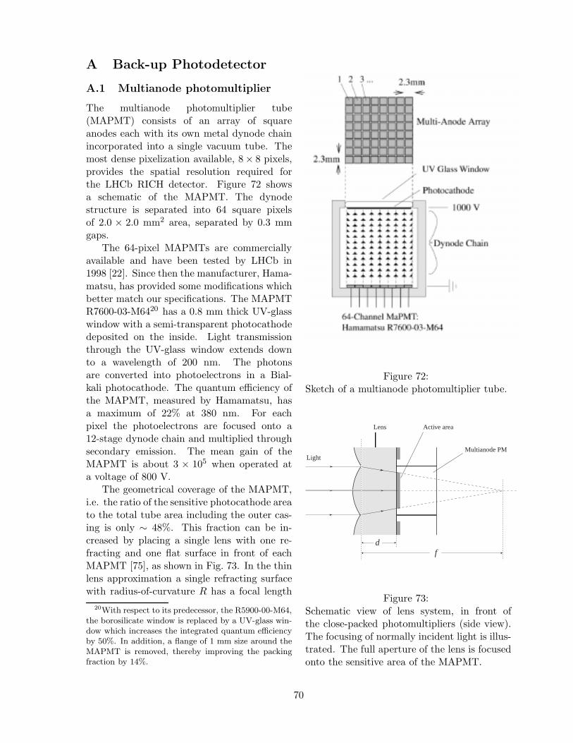
A Back-up Photodetector
A.1 Multianode photomultiplier
The multianode photomultiplier tube(MAPMT) consists of an array of squareanodes each with its own metal dynode chainincorporated into a single vacuum tube. Themost dense pixelization available, 8× 8 pixels,provides the spatial resolution required forthe LHCb RICH detector. Figure 72 showsa schematic of the MAPMT. The dynodestructure is separated into 64 square pixelsof 2.0 × 2.0 mm2 area, separated by 0.3 mmgaps.
The 64-pixel MAPMTs are commerciallyavailable and have been tested by LHCb in1998 [22]. Since then the manufacturer, Hama-matsu, has provided some modifications whichbetter match our specifications. The MAPMTR7600-03-M6420 has a 0.8 mm thick UV-glasswindow with a semi-transparent photocathodedeposited on the inside. Light transmissionthrough the UV-glass window extends downto a wavelength of 200 nm. The photonsare converted into photoelectrons in a Bial-kali photocathode. The quantum efficiency ofthe MAPMT, measured by Hamamatsu, hasa maximum of 22% at 380 nm. For eachpixel the photoelectrons are focused onto a12-stage dynode chain and multiplied throughsecondary emission. The mean gain of theMAPMT is about 3 × 10⁵ when operated ata voltage of 800 V.
The geometrical coverage of the MAPMT,i.e. the ratio of the sensitive photocathode areato the total tube area including the outer cas-ing is only ∼ 48%. This fraction can be in-creased by placing a single lens with one re-fracting and one flat surface in front of eachMAPMT [75], as shown in Fig. 73. In the thinlens approximation a single refracting surfacewith radius-of-curvature R has a focal length
20With respect to its predecessor, the R5900-00-M64,the borosilicate window is replaced by a UV-glass win-dow which increases the integrated quantum efficiencyby 50%. In addition, a flange of 1 mm size around theMAPMT is removed, thereby improving the packingfraction by 14%.
Figure 72:Sketch of a multianode photomultiplier tube.
df
Multianode PM
Active areaLens
Light
Figure 73:Schematic view of lens system, in front ofthe close-packed photomultipliers (side view).The focusing of normally incident light is illus-trated. The full aperture of the lens is focusedonto the sensitive area of the MAPMT.
70
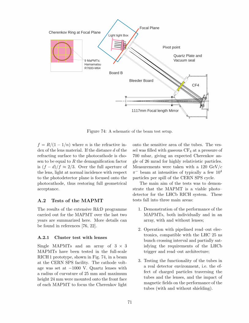
Focal Plane
Light tight Box
Pivot point
Quartz Plate and Vacuum seal
Board B
Bleeder BoardCF4
1117mm Focal length Mirror
Cherenkov Ring at Focal Plane
9 MaPMTs: Hamamatsu R7600-M64
Figure 74: A schematic of the beam test setup.
f = R/(1 − 1/n) where n is the refractive in-dex of the lens material. If the distance d of therefracting surface to the photocathode is cho-sen to be equal to R the demagnification factoris (f − d)/f ≈ 2/3. Over the full aperture ofthe lens, light at normal incidence with respectto the photodetector plane is focused onto thephotocathode, thus restoring full geometricalacceptance.
A.2 Tests of the MAPMT
The results of the extensive R&D programmecarried out for the MAPMT over the last twoyears are summarized here. More details canbe found in references [76, 22].
A.2.1 Cluster test with lenses
Single MAPMTs and an array of 3 × 3MAPMTs have been tested in the full-scaleRICH1 prototype, shown in Fig. 74, in a beamat the CERN SPS facility. The cathode volt-age was set at −1000 V. Quartz lenses witha radius of curvature of 25 mm and maximumheight 24 mm were mounted onto the front faceof each MAPMT to focus the Cherenkov light
onto the sensitive area of the tubes. The ves-sel was filled with gaseous CF4 at a pressure of700 mbar, giving an expected Cherenkov an-gle of 26 mrad for highly relativistic particles.Measurements were taken with a 120 GeV/cπ− beam at intensities of typically a few 104
particles per spill of the CERN SPS cycle.The main aim of the tests was to demon-
strate that the MAPMT is a viable photo–detector for the LHCb RICH system. Thesetests fall into three main areas:
1. Demonstration of the performance of theMAPMTs, both individually and in anarray, with and without lenses;
2. Operation with pipelined read–out elec-tronics, compatible with the LHC 25 nsbunch crossing interval and partially sat-isfying the requirements of the LHCbtrigger and read–out architecture;
3. Testing the functionality of the tubes ina real detector environment, i.e. the ef-fect of charged particles traversing thetubes and the lenses, and the impact ofmagnetic fields on the performance of thetubes (with and without shielding).
71
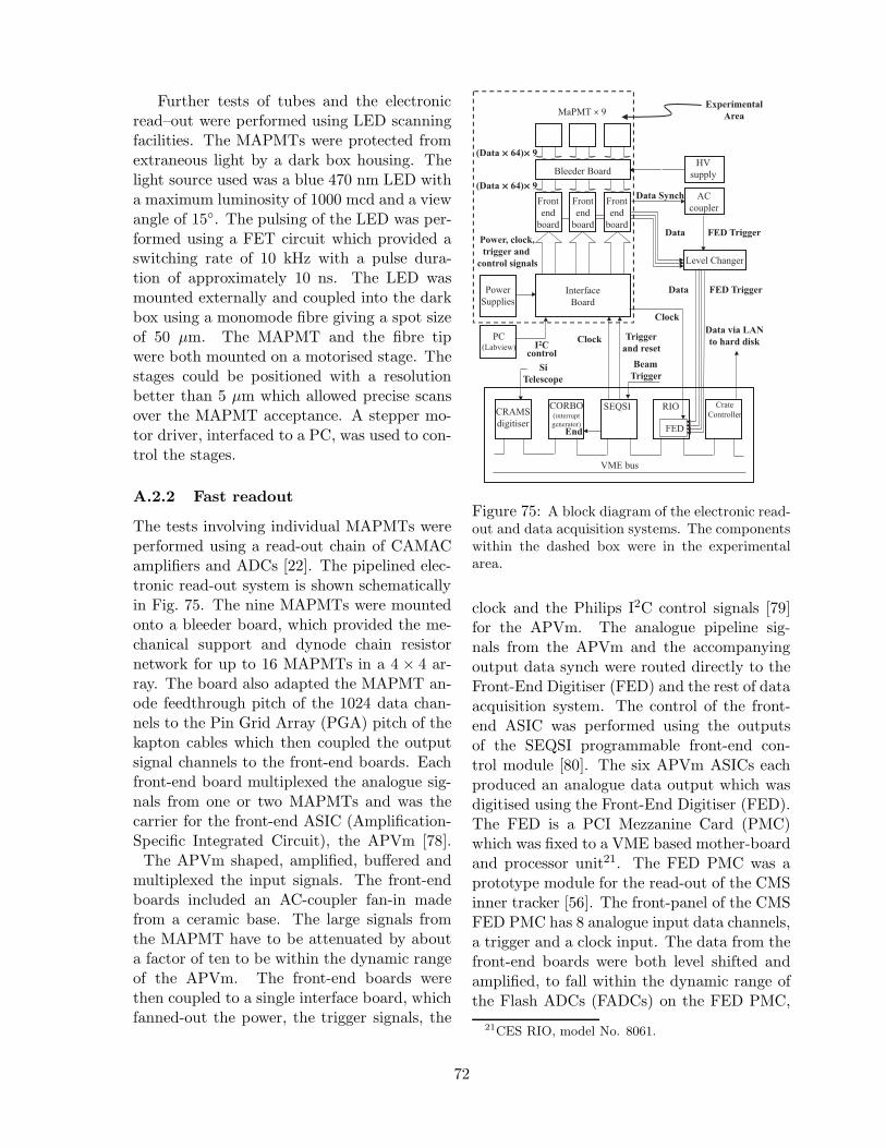
Further tests of tubes and the electronicread–out were performed using LED scanningfacilities. The MAPMTs were protected fromextraneous light by a dark box housing. Thelight source used was a blue 470 nm LED witha maximum luminosity of 1000 mcd and a viewangle of 15. The pulsing of the LED was per-formed using a FET circuit which provided aswitching rate of 10 kHz with a pulse dura-tion of approximately 10 ns. The LED wasmounted externally and coupled into the darkbox using a monomode fibre giving a spot sizeof 50 µm. The MAPMT and the fibre tipwere both mounted on a motorised stage. Thestages could be positioned with a resolutionbetter than 5 µm which allowed precise scansover the MAPMT acceptance. A stepper mo-tor driver, interfaced to a PC, was used to con-trol the stages.
A.2.2 Fast readout
The tests involving individual MAPMTs wereperformed using a read-out chain of CAMACamplifiers and ADCs [22]. The pipelined elec-tronic read-out system is shown schematicallyin Fig. 75. The nine MAPMTs were mountedonto a bleeder board, which provided the me-chanical support and dynode chain resistornetwork for up to 16 MAPMTs in a 4 × 4 ar-ray. The board also adapted the MAPMT an-ode feedthrough pitch of the 1024 data chan-nels to the Pin Grid Array (PGA) pitch of thekapton cables which then coupled the outputsignal channels to the front-end boards. Eachfront-end board multiplexed the analogue sig-nals from one or two MAPMTs and was thecarrier for the front-end ASIC (Amplification-Specific Integrated Circuit), the APVm [78].The APVm shaped, amplified, buffered and
multiplexed the input signals. The front-endboards included an AC-coupler fan-in madefrom a ceramic base. The large signals fromthe MAPMT have to be attenuated by abouta factor of ten to be within the dynamic rangeof the APVm. The front-end boards werethen coupled to a single interface board, whichfanned-out the power, the trigger signals, the
Figure 75: A block diagram of the electronic read-out and data acquisition systems. The componentswithin the dashed box were in the experimentalarea.
clock and the Philips I2C control signals [79]for the APVm. The analogue pipeline sig-nals from the APVm and the accompanyingoutput data synch were routed directly to theFront-End Digitiser (FED) and the rest of dataacquisition system. The control of the front-end ASIC was performed using the outputsof the SEQSI programmable front-end con-trol module [80]. The six APVm ASICs eachproduced an analogue data output which wasdigitised using the Front-End Digitiser (FED).The FED is a PCI Mezzanine Card (PMC)which was fixed to a VME based mother-boardand processor unit21. The FED PMC was aprototype module for the read-out of the CMSinner tracker [56]. The front-panel of the CMSFED PMC has 8 analogue input data channels,a trigger and a clock input. The data from thefront-end boards were both level shifted andamplified, to fall within the dynamic range ofthe Flash ADCs (FADCs) on the FED PMC,
21CES RIO, model No. 8061.
72
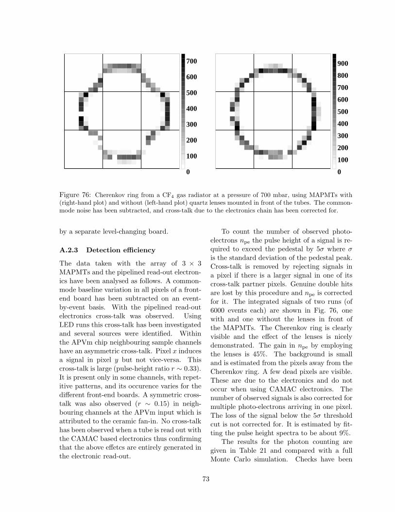
0
100
200
300
400
500
600
700
0
100
200
300
400
500
600
700
800
900
Figure 76: Cherenkov ring from a CF4 gas radiator at a pressure of 700 mbar, using MAPMTs with(right-hand plot) and without (left-hand plot) quartz lenses mounted in front of the tubes. The common-mode noise has been subtracted, and cross-talk due to the electronics chain has been corrected for.
by a separate level-changing board.
A.2.3 Detection efficiency
The data taken with the array of 3 × 3MAPMTs and the pipelined read-out electron-ics have been analysed as follows. A common-mode baseline variation in all pixels of a front-end board has been subtracted on an event-by-event basis. With the pipelined read-outelectronics cross-talk was observed. UsingLED runs this cross-talk has been investigatedand several sources were identified. Withinthe APVm chip neighbouring sample channelshave an asymmetric cross-talk. Pixel x inducesa signal in pixel y but not vice-versa. Thiscross-talk is large (pulse-height ratio r ∼ 0.33).It is present only in some channels, with repet-itive patterns, and its occurence varies for thedifferent front-end boards. A symmetric cross-talk was also observed (r ∼ 0.15) in neigh-bouring channels at the APVm input which isattributed to the ceramic fan-in. No cross-talkhas been observed when a tube is read out withthe CAMAC based electronics thus confirmingthat the above effetcs are entirely generated inthe electronic read-out.
To count the number of observed photo-electrons npe the pulse height of a signal is re-quired to exceed the pedestal by 5σ where σis the standard deviation of the pedestal peak.Cross-talk is removed by rejecting signals ina pixel if there is a larger signal in one of itscross-talk partner pixels. Genuine double hitsare lost by this procedure and npe is correctedfor it. The integrated signals of two runs (of6000 events each) are shown in Fig. 76, onewith and one without the lenses in front ofthe MAPMTs. The Cherenkov ring is clearlyvisible and the effect of the lenses is nicelydemonstrated. The gain in npe by employingthe lenses is 45%. The background is smalland is estimated from the pixels away from theCherenkov ring. A few dead pixels are visible.These are due to the electronics and do notoccur when using CAMAC electronics. Thenumber of observed signals is also corrected formultiple photo-electrons arriving in one pixel.The loss of the signal below the 5σ thresholdcut is not corrected for. It is estimated by fit-ting the pulse height spectra to be about 9%.
The results for the photon counting aregiven in Table 21 and compared with a fullMonte Carlo simulation. Checks have been
73
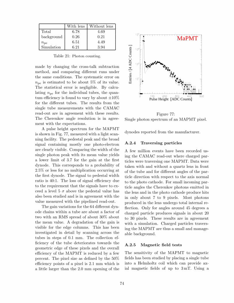
With lens Without lensTotal 6.78 4.69background 0.26 0.21npe 6.51 4.49Simulation 6.21 3.94
Table 21: Photon counting.
made by changing the cross-talk subtractionmethod, and comparing different runs underthe same conditions. The systematic error onnpe is estimated to be about 5% of its value.The statistical error is negligible. By calcu-lating npe for the individual tubes, the quan-tum efficiency is found to vary by about ±10%for the different tubes. The results from thesingle tube measurements with the CAMACread-out are in agreement with these results.The Cherenkov angle resolution is in agree-ment with the expectations.
A pulse height spectrum for the MAPMTis shown in Fig. 77, measured with a light scan-ning facility. The pedestal peak and the broadsignal containing mostly one photo-electronare clearly visible. Comparing the width of thesingle photon peak with its mean value yieldsa lower limit of 3.7 for the gain at the firstdynode. This corresponds to a probability of2.5% or less for no multiplication occurring atthe first dynode. The signal to pedestal widthratio is 40:1. The loss of signal efficiency dueto the requirement that the signals have to ex-ceed a level 5 σ above the pedestal value hasalso been studied and is in agreement with thevalue measured with the pipelined read-out.
The gain variations for the 64 different dyn-ode chains within a tube are about a factor oftwo with an RMS spread of about 30% aboutthe mean value. A degradation of the gain isvisible for the edge columns. This has beeninvestigated in detail by scanning across thetubes in steps of 0.1 mm. The collection ef-ficiency of the tube deteriorates towards thegeometric edge of these pixels and the overallefficiency of the MAPMT is reduced by a fewpercent. The pixel size as defined by the 50%efficiency points of a pixel is 2.1 mm which isa little larger than the 2.0 mm opening of the
Pulse Height [ADC Counts]
Ent
ries
/ [4 A
DC
Cou
nts ]
MaPMT
Figure 77:Single photon spectrum of an MAPMT pixel.
dynodes reported from the manufacturer.
A.2.4 Traversing particles
A few million events have been recorded us-ing the CAMAC read-out where charged par-ticles were traversing one MAPMT. Data weretaken with and without a quartz lens in frontof the tube and for different angles of the par-ticle direction with respect to the axis normalto the photo cathode. For small incoming par-ticle angles the Cherenkov photons emitted inthe lens and in the photo cathode produce hitsin only about 7 to 9 pixels. Most photonsproduced in the lens undergo total internal re-flection. Only for angles around 45 degrees acharged particle produces signals in about 20to 30 pixels. These results are in agreementwith a simulation. Charged particles travers-ing the MAPMT are thus a small and manage-able background.
A.2.5 Magnetic field tests
The sensitivity of the MAPMT to magneticfields has been studied by placing a single tubeinto a Helmholtz coil which can provide ax-ial magnetic fields of up to 3mT. Using a
74
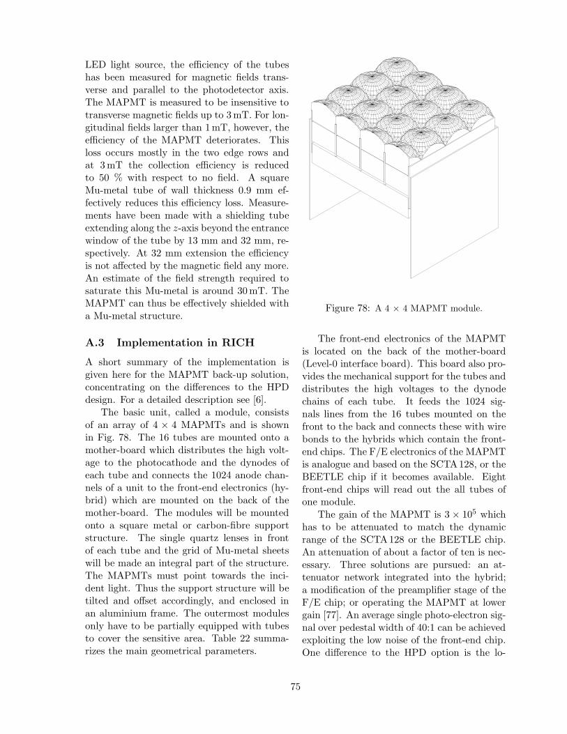
LED light source, the efficiency of the tubeshas been measured for magnetic fields trans-verse and parallel to the photodetector axis.The MAPMT is measured to be insensitive totransverse magnetic fields up to 3 mT. For lon-gitudinal fields larger than 1mT, however, theefficiency of the MAPMT deteriorates. Thisloss occurs mostly in the two edge rows andat 3 mT the collection efficiency is reducedto 50 % with respect to no field. A squareMu-metal tube of wall thickness 0.9 mm ef-fectively reduces this efficiency loss. Measure-ments have been made with a shielding tubeextending along the z-axis beyond the entrancewindow of the tube by 13 mm and 32 mm, re-spectively. At 32 mm extension the efficiencyis not affected by the magnetic field any more.An estimate of the field strength required tosaturate this Mu-metal is around 30 mT. TheMAPMT can thus be effectively shielded witha Mu-metal structure.
A.3 Implementation in RICH
A short summary of the implementation isgiven here for the MAPMT back-up solution,concentrating on the differences to the HPDdesign. For a detailed description see [6].
The basic unit, called a module, consistsof an array of 4 × 4 MAPMTs and is shownin Fig. 78. The 16 tubes are mounted onto amother-board which distributes the high volt-age to the photocathode and the dynodes ofeach tube and connects the 1024 anode chan-nels of a unit to the front-end electronics (hy-brid) which are mounted on the back of themother-board. The modules will be mountedonto a square metal or carbon-fibre supportstructure. The single quartz lenses in frontof each tube and the grid of Mu-metal sheetswill be made an integral part of the structure.The MAPMTs must point towards the inci-dent light. Thus the support structure will betilted and offset accordingly, and enclosed inan aluminium frame. The outermost modulesonly have to be partially equipped with tubesto cover the sensitive area. Table 22 summa-rizes the main geometrical parameters.
Figure 78: A 4 × 4 MAPMT module.
The front-end electronics of the MAPMTis located on the back of the mother-board(Level-0 interface board). This board also pro-vides the mechanical support for the tubes anddistributes the high voltages to the dynodechains of each tube. It feeds the 1024 sig-nals lines from the 16 tubes mounted on thefront to the back and connects these with wirebonds to the hybrids which contain the front-end chips. The F/E electronics of the MAPMTis analogue and based on the SCTA128, or theBEETLE chip if it becomes available. Eightfront-end chips will read out the all tubes ofone module.
The gain of the MAPMT is 3 × 10⁵ whichhas to be attenuated to match the dynamicrange of the SCTA128 or the BEETLE chip.An attenuation of about a factor of ten is nec-essary. Three solutions are pursued: an at-tenuator network integrated into the hybrid;a modification of the preamplifier stage of theF/E chip; or operating the MAPMT at lowergain [77]. An average single photo-electron sig-nal over pedestal width of 40:1 can be achievedexploiting the low noise of the front-end chip.One difference to the HPD option is the lo-
75

MAPMT Modules:Module size [mm2] 109 × 109Active/total area 0.79Quadrants/Halfplane: RICH1 RICH2Horizontal tilt [mrad] ± 440 ± 240Vertical tilt [mrad] ± 125 0Modules per row 5 6Modules per column 5 11Totals: RICH1 RICH2Modules 100 132Tubes 1480 2024RICH totals:Modules 232Tubes 3504Channels 224256
Table 22: MAPMT Geometry.
cation of the off-detector electronics (ODE).For analogue signals, copper links will be usedbetween Level-0 F/E and Level-1 ODE. Thislimits the distance between these to a lengthof 12 m. The Level-1 electronics will requirereceivers and ADCs for the front-end and willneed to be designed to tolerate problems dueto radiation, particularly single event upsets.Access will be severely restricted.
A binary readout scheme for the MAPMTwill also be studied. This has several potentialbenefits, including:
1. The use of fibre-optic links and theradiation-hard fibre driver technology fordata transfer between Level-0 and Level-1, as proposed for the HPDs.
2. Level-1 electronics in the counting roomfacilitates access and commissioning.
3. Re-use of the expertise and designs de-veloped for the HPD.
4. Simplified grounding.
In Table 24 a schedule for the MAPMTback-up project is presented. The front-endchip and the mother-board/hybrid are now themost time-critical parts of the project. A few
Level-0 & Front-end chipModules / chips 232 / 1856Channels per module 1024Readout channels 237568Multiplexing 32-foldData links to Level-1 7424Level 1Bandwidth (3% occupancy,without/with zero suppr.) 85 / 7.7 Gbits/sVME modules 78Multiplexers 5
Table 23: MAPMT Electronics.
working mother-boards and hybrids plus front-end chips are needed before the testing of largequantities of MAPMTs can start. Of thesethe mother-board/hybrid is the most seriousas there is little possibility of saving time. Theschedule of the front-end chip would be short-ened if the MAPMT could be operated at lowergain without the need of a redesign or attenu-ator network (see Reference [77]). The test ofa RICH1 half-plane in the 2003 test beams atCERN is also critical since the production andtesting of the final modules would not start be-fore 1/2003. The ODE schedule would greatlybenefit with the binary readout option (for rea-sons listed above).
76
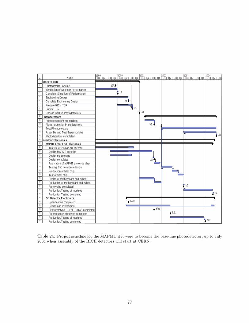
ID Name1 Work to TDR2 Photodetector Choice3 Simulation of Detector Performance4 Complete Simultion of Performance5 Engineering Design6 Complete Engineering Design7 Prepare RICH TDR8 Submit TDR9 Choose Backup Photodetectors
10 Photodetector s11 Prepare specs/invite tenders12 Place orders for Photodetectors13 Test Photodetectors14 Assemble and Test Supermodules15 Photodetectors completed16 Readout Electronics17 MaPMT Front End Electronics18 Test 40 MHz Read-out (APVm)19 Design MAPMT specifics20 Design multiplexing21 Design completed22 Fabrication of MAPMT prototype chip23 Testing/ 2nd iteration redesign24 Production of final chip25 Test of final chip26 Design of motherboard and hybrid27 Production of motherboard and hybrid28 Prototyping completed29 Production/Testing of modules30 Production Testing completed31 Off Detector Electronics32 Specification completed33 Design and Prototyping34 First prototype ODE/TTC/DCS completed35 Preproduction prototype completed36 Production/Testing of modules37 Production/Testing completed
12/1
1/1
7/1
9/11/1
9/3
7/1
9/3
1/6
5/4
6/30
8/315/31
1/1
Q1 Q2 Q3 Q4 Q1 Q2 Q3 Q4 Q1 Q2 Q3 Q4 Q1 Q2 Q3 Q4 Q1 Q2 Q3 Q4 Q1 Q2 Q31999 2000 2001 2002 2003 2004
Table 24: Project schedule for the MAPMT if it were to become the base-line photodetector, up to July2004 when assembly of the RICH detectors will start at CERN.
77
References
[1] LHCb Technical Proposal, CERN/LHCC98-4.
[2] LHCb Magnet Technical Design Report,CERN/LHCC 2000-7.
[3] LHCb Calorimeters Technical Design Re-port, CERN/LHCC 2000-36.
[4] C.Joram et al., “Proposal to use thePad HPD as Photodetector of the LHCbRICH”, LHCb 2000–63 RICH.
[5] T.Gys et al., “The use of Pixel HybridPhoton Detectors in the RICH countersof LHCb”, LHCb 2000–64 RICH.
[6] F.Muheim et al., “Proposal for Multi-Anode Photomultiplier tubes as Photode-tectors for the LHCb RICH”, LHCb 2000–65 RICH.
[7] T.Ypsilantis and J.Seguinot, Nucl. Instr.Meth. A 343 (1994) 30.
[8] J.Christiansen, “Requirements for the L0front-end electronics”, LHCb 99–29.
[9] K.Wyllie, “Level 0 electronics for theLHCb RICH” LHCb 2000-75 RICH.
[10] G.Wilkinson et al., “A simulation studyof the LHCb RICH performance”, LHCb2000–66 RICH.
[11] T.Sjostrand and M.Bengtsson, Comp.Phys. Comm. 43 (1987) 367.
[12] P.Bartalini et al., “Tuning of multiple in-teractions generated by PYTHIA”, LHCb99–28.
[13] R.Forty and O.Schneider, “RICH patternrecognition”, LHCb 98–40.
[14] M.Benayoun, “Search for trackless rings”,presentation at LHCb RICH meeting, 30November, 1999.
[15] A.Schoning, “Particle identification in theRICH detectors and study of impact pa-rameters”, LHCb 97–18.
[16] M.Tobar, “B flavour tagging with kaons”,LHCb 98–18.
[17] GAUDI User Guide, http://lhcb.cern.ch/computing/Components/Gaudi v5/gug.pdf
[18] I.Jacobson, G.Booch and G.Rumbaugh,“The Unified Software Development Pro-cess”, Addison-Wesley, Reading MA,1999.
[19] E.Gamma, R.Helm, R.Johnson andJ.Vlissides, “Design Patterns”, Addison-Wesley, Reading MA, 1995.
[20] D.Liko and N.Neufeld, “Design of theObject-Oriented RICH reconstruction”,LHCb 2000–67.
[21] E.Albrecht et al., Nucl. Instr. and Meth.A 411 (1998) 249.
[22] E.Albrecht et. al., “A prototype RICHdetector Using Multi-Anode Photo Mul-tiplier Tubes and Hybrid Photo-Diodes”,LHCb 2000–68 RICH, submitted to Nucl.Instr. and Meth. A.
[23] O.Toker et al., Nucl. Instr. and Meth. A340 (1994) 572.
[24] E.Chesi et al., “The 5-inch 2048-pad HPDdevelopment project”, LHCb 98–37.
[25] T.Bellunato et al., “Optical characteriza-tion of aerogel as Cherenkov radiator”,LHCb 2000–73.
[26] T.Bellunato et al., “Beam tests with aero-gel RICH radiator”, LHCb 2000–76.
[27] I.P.Csorba, “Image Tubes”, Howard W.Sams & Co., 1985.
[28] T.Gys and D.Piedigrossi, “Performance ofelectrostatically-focused Image IntensifierTubes in Low Magnetic Fields”, LHCb97–26.
[29] E.Heijne et al., Nucl. Instr. and Meth. A383 (1996) 55.
78
[30] M.Alemi et al. “First operation of a hy-brid photon detector prototype with elec-trostatic cross-focussing and integratedsilicon pixel readout”, Nucl. Instr. andMeth. A 449 (2000) 48.
[31] C.Iselin, “Solution of Poisson’s orLaplace’s equation in two-dimentionalregions”, CERN Program Library longwrite-up T604, 1984.
[32] T.Seidel, “Calculation of PhotoelectronPaths in Cylindrical Coordinates”, CERNEF/IN internal report, 1990, Program up-graded by T.Gys.
[33] M.Alemi em et al., IEEE Trans. Nucl. Sc.vol 46 no.6, (1999), 1901.
[34] E.Albrecht,et al., Nucl. Instr. and Meth.A 442 (2000) 164.
[35] S.Easo, et al., “Tests of full-scale PixelHPD prototype”. LHCb 2000–70.
[36] M.Alemi et al., Nucl. Phys. B (ProcSuppl.) 78 (1999) 360.
[37] ALICE- Technical Proposal for A LargeION Collider Experiment at the CERNLHC, CERN/LHCC 95-71, December1995.
[38] T.Gys and D.Piedigrossi, “Performance offull-scale pixel HPD tubes in low magneticfields”, LHCb 2000–69 RICH.
[39] Technical Design Report for the InnerTracking System(ITS), CERN/LHCC 99-12, June 1999.
[40] K.Wyllie et.al, “A pixel readout chip fortracking at ALICE and particle identifi-cation at LHCb”,Proceedings of the fifthworkshop on Electronics for LHC Exper-iments, Snowmass, Colorado, September1999, CERN/LHCC/99–33.
[41] M.Campbell et. al, IEEE Trans. Nucl. Sc.vol 45 no. 3 (1998) 751.
[42] W.Snoeys et.al. Nucl. Instr. and Meth. A439 (2000) 349.
[43] M.Campbell et. al, IEEE Trancs. Nucl.Sc. vol 46 no. 3 (1999)156.
[44] C.D’Ambrosio, L.Fernandez, M.Laub,D.Piedigrossi, “The optical systems ofLHCb RICHes: a study on the mirrorwalls and mirror specifications”, LHCb2000–71.
[45] C.D’Ambrosio, M.Laub, D.Piedigrossi,P.Wertelaers, P.Wicht, “An experimentalset-up to measure the long-term stabilityof large-mirror supports”, LHCb 2000–20.
[46] C.D’Ambrosio, M.Laub, D.Piedigrossi,P.Wertelaers, P.Wicht, “Characterizationof mirror mount prototypes for RICH de-tectors”, LHCb 2000–72.
[47] J.Christiansen, et al., “TTCrx Ref-erence Manual”, RD12 project.http://www.cern.ch/TTC/TTCrx manual3.0.pdf
[48] “JTAG: IEEE Standard Test Access Portand Boundary Scan Architecture”, IEEEStd. 1149.1 (1990).
[49] “The LHCb Experimental Controls Sys-tem”,http://lhcb.cern.ch/computing/controls/default.htm.
[50] J.Bibby, S.Wotton, “RICH Electronics:Requirements, Specifications and Imple-mentation”, LHCb 2000–74 RICH.
[51] A.Kluge, “Status of PILOT Electronics”,Presentation at ALICE SPD meeting,May 15, 2000.
[52] P.Denes, “Digitisation and Data Trans-mission for the CMS ECAL”, Proceedingsof the Fourth Workshop on Electronics forLHC Experiments, Rome, Italy, October1998, CERN/LHCC/98–36.
[53] P.Moriera, et al., “A 1.25 Gbit/s Serial-izer for LHC Data and Trigger OpticalLinks”, Proceedings of the Fifth Work-shop on Electronics for LHC Experiments,
79
Snowmass, Colorado, September 1999,CERN/LHCC/99–33.
[54] H.Muller, “LHCb Readout Units”,http://hmuller.home.cern.ch/hmuller/readout unit.htm.
[55] O.Boyle et al., “The S-LINK InterfaceSpecification”,http://www.cern.ch/HSI/s-link/spec,March 1997.
[56] J.Coughlan, “CMS Front-End DriverPMC”, User Manual, Rutherford Apple-ton Laboratory, Unpublished.
[57] G.Barber, et al., “The mechanical designof RICH-1” , LHCb 2000–77 RICH.
[58] G.Barber, A.Duane, J.Lidbury, “The in-stallation of RICH1 and the Beampipe”.LHCb 2000–78 RICH.
[59] M.Bosteels, F.Hahn, S.Haider, R.Lindner,O.Ullaland, “LHCb RICH Gas systemproposal” LHCb 2000–79 RICH.
[60] C.D’Ambrosio, et al., “Monitoring, Align-ment and Control of the RICH Detec-tors”, LHCb 2000–80 RICH.
[61] O.Ullaland, et al., “LHCb RICH2 Me-chanics” LHCb 2000–81 RICH.
[62] M.Alemi, “Passive magnetic shieldingcalculation for the photodetectors ofRICH2”, LHCb 98–17 RICH.
M.Alemi, Tecniche di rivelazione neiRICH di LHCb, PhD thesis, Milano 1999.
[63] S.Cuneo, M.Ameri, V.Gracco, P.Musico,A.Petrolini, M.Sannino, “A proposal for asupporting structure for the Hybrid PixelDetector (HPD) of RICH2”. LHCb 2000–82 RICH.
[64] H.Kroha, Nucl. Phys. B (Proc. Suppl.) 54(1997) 80.
[65] W.Blum et al., Nucl. Instr. and Meth. A377 (1996) 404.
[66] W.Blum et al., Nucl. Instr. and Meth. A367 (1995) 413.
[67] A.Gorisek et al., Nucl. Instr. and Meth. A433 (1999) 408.
[68] F.Filthaut, Presentation at LHCb RICHmeeting, 19 March 1999.http://lhcb.cern.ch/rich/postscript/filthaut 190399.ps
[69] M.L.Andrieux et al., Nucl. Instr. andMeth. A 371 (1996) 259.
[70] E.Fokitis et al., Nucl. Phys. B (Proc.Suppl.) 44 (1995) 246.
[71] A.Filippas et al., Nucl. Instr. and Meth.A 371 (1996) 255.
[72] G.Lenzen et al., Nucl. Instr. and Meth. A343 (1994) 268.
[73] G.Barichello et al., Nucl. Instr. and Meth.A 419 (1998) 1.
[74] C.Gaspar, LHCb Frontend ElectronicsWorkshop, 16-19 May 2000.http://lhcb.cern.ch/computing/online/html/Workshop%20Agenda.htm
[75] R.Forty, “Use of lenses to increase theRICH photodetector coverage”, LHCb98–38.
[76] A.Albrecht, et al. “Test of a Multi-AnodePMT cluster equipped with lenses inthe detection of Cherenkov rings”. LHCb2000–83 RICH.
[77] S.Eisenhardt, J.Libby, F.Muheim “Studyof Multi Anode Photo Multiplier Tubes atLow Gains”, LHCb 2000–88 RICH.
[78] L.L.Jones et al., “Electronics forLHC Experiments”, Rome 1998,CERN/LHCC/98–36 (1998) 185.
[79] Philips Semiconductors, “The I2C-Busspecification”, version 2.1, January 2000.
[80] M.Morrisey, “SEQSI Manual”, Ruther-ford Appleton Laboratory, Unpublished.
80