Embed Size (px)
Citation preview

Light-trapping optimization in wet-etched silicon photonic crystal solar cellsSergey Eyderman, Sajeev John, M. Hafez, S. S. Al-Ameer, T. S. Al-Harby, Y. Al-Hadeethi, and D. M. Bouwes Citation: Journal of Applied Physics 118, 023103 (2015); doi: 10.1063/1.4926548 View online: http://dx.doi.org/10.1063/1.4926548 View Table of Contents: http://scitation.aip.org/content/aip/journal/jap/118/2?ver=pdfcov Published by the AIP Publishing Articles you may be interested in An efficient light trapping scheme based on textured conductive photonic crystal back reflector for performanceimprovement of amorphous silicon solar cells Appl. Phys. Lett. 105, 073506 (2014); 10.1063/1.4893606 Solar light trapping in slanted conical-pore photonic crystals: Beyond statistical ray trapping J. Appl. Phys. 113, 154315 (2013); 10.1063/1.4802442 Photonic assisted light trapping integrated in ultrathin crystalline silicon solar cells by nanoimprint lithography Appl. Phys. Lett. 101, 103901 (2012); 10.1063/1.4749810 Integrated photonic structures for light trapping in thin-film Si solar cells Appl. Phys. Lett. 100, 111110 (2012); 10.1063/1.3693613 Photonic crystal enhanced light-trapping in thin film solar cells J. Appl. Phys. 103, 093102 (2008); 10.1063/1.2908212
[This article is copyrighted as indicated in the article. Reuse of AIP content is subject to the terms at: http://scitation.aip.org/termsconditions. Downloaded to ] IP:
128.100.78.127 On: Tue, 14 Jul 2015 13:58:48
Light-trapping optimization in wet-etched silicon photonic crystal solar cells
Sergey Eyderman,1,a) Sajeev John,1,2 M. Hafez,2 S. S. Al-Ameer,2 T. S. Al-Harby,2
Y. Al-Hadeethi,2 and D. M. Bouwes3
1Department of Physics, University of Toronto, 60 St. George Street, Toronto, Ontario M5S 1A7, Canada2Department of Physics, King Abdul-Aziz University, Jeddah, Saudi Arabia3iX-factory GmbH, Konrad Adenauer–Allee 11, 44263 Dortmund, Germany
(Received 6 March 2015; accepted 24 June 2015; published online 10 July 2015)
We demonstrate, by numerical solution of Maxwell’s equations, near-perfect solar light-trapping
and absorption over the 300–1100 nm wavelength band in silicon photonic crystal (PhC) architec-
tures, amenable to fabrication by wet-etching and requiring less than 10 lm (equivalent bulk thick-
ness) of crystalline silicon. These PhC’s consist of square lattices of inverted pyramids with sides
comprised of various (111) silicon facets and pyramid center-to-center spacing in the range of
1.3–2.5 lm. For a wet-etched slab with overall height H¼ 10 lm and lattice constant a¼ 2.5 lm,
we find a maximum achievable photo-current density (MAPD) of 42.5 mA/cm2, falling not far
from 43.5 mA/cm2, corresponding to 100% solar absorption in the range of 300–1100 nm. We also
demonstrate a MAPD of 37.8 mA/cm2 for a thinner silicon PhC slab of overall height H¼ 5 lm
and lattice constant a¼ 1.9 lm. When H is further reduced to 3 lm, the optimal lattice constant for
inverted pyramids reduces to a¼ 1.3 lm and provides the MAPD of 35.5 mA/cm2. These wet-
etched structures require more than double the volume of silicon, in comparison to the overall
mathematically optimum PhC structure (consisting of slanted conical pores), to achieve the same
degree of solar absorption. It is suggested these 3–10 lm thick structures are valuable alternatives
to currently utilized 300 lm-thick textured solar cells and are suitable for large-scale fabrication by
wet-etching. VC 2015 AIP Publishing LLC. [http://dx.doi.org/10.1063/1.4926548]
I. INTRODUCTION
Multiple light scattering and wave interference effects
provide a fundamental mechanism for light trapping. In a
weakly absorbing medium, the resulting long dwell time for
light enables significant absorption enhancement.1 Photonic
crystals (PhC’s)2,3 are special class of light-trapping materials
in which this capability is often associated with suppression of
the electromagnetic density of states.4 A less widely studied
form of photonic crystal light-trapping occurs when this den-
sity of states is enhanced rather than suppressed.5 This alterna-
tive form of light trapping is useful for absorption of light
from a broadband external source6–8 and has been exploited
for the design of thin-film (200 nm–1 lm) solar cells with
high power conversion efficiencies.9,10 Other applications of
photonic crystals include optical interconnects,11 imaging
devices,12 optical sensors,13 and biosensors.14 In this paper,
we show that suitably structured, intermediate thickness (�10
lm) silicon photonic crystals can achieve solar light-trapping
and absorption comparable to and possibly surpassing the best
available15 thick (300–450 lm) silicon solar cells.
Crystalline silicon wafers are currently the most widely
used materials in the solar cell industry with up to 25%
power conversion efficiency in a 300 lm thick wafer.16
However, untextured crystalline silicon wafers have high so-
lar reflectivity, around 40%, in the visible wavelength range
and very weak absorption in the red to infrared spectral
range. In order to improve the cell efficiency, anti-reflective
surface texturing17 is applied to crystalline silicon solar cells
to reduce light reflection18–20 at the wafer surface. If the lat-
tice constant of surface texturing is large compared to the
wavelengths of incident photons, the texture will induce light
reflection between the surfaces of the texture, resulting in so-
lar ray-trapping21–26 and reduced light reflection.
On the other hand, if the period of the surface texture is
comparable to or smaller than the wavelengths of incident
photons, enhanced solar light-trapping can occur through
multiple scattering and wave interference. In addition to
reduced light reflection due to a graded refractive index near
the surface, parallel-to-interface refraction (PIR)5 and slow-
light effects6,19 lead to a strong light absorption in thin-film
(�1 lm) silicon PhC solar cells even at near infrared wave-
lengths. This anomalous type of refraction is negative and
usually out of the plane of incidence. Sunlight impinging on
photonic crystal interface, couples to Bloch modes propagat-
ing nearly parallel to the interface. This leads to anomalously
long optical path lengths and long dwell times before the
light beam exits the thin film. This effect becomes especially
pronounced in the wavelength region where intrinsic absorp-
tion of silicon is weak, manifesting itself as strong absorption
peaks in the infrared region.
The PIR effect cannot be captured by ordinary ray trac-
ing methods. This effect has purely wave nature and mani-
fests itself as a parallel-to-interface energy flow as well as its
circulation in certain areas.7 Also despite the fact that the lat-
tice constant is greater than a typical wavelength, our struc-
ture, described below (see Fig. 2), has areas (close to the tips
a)Author to whom correspondence should be addressed. Electronic mail:
0021-8979/2015/118(2)/023103/7/$30.00 VC 2015 AIP Publishing LLC118, 023103-1
JOURNAL OF APPLIED PHYSICS 118, 023103 (2015)
[This article is copyrighted as indicated in the article. Reuse of AIP content is subject to the terms at: http://scitation.aip.org/termsconditions. Downloaded to ] IP:
128.100.78.127 On: Tue, 14 Jul 2015 13:58:48
of pyramids where they are narrowing), where the wavelength
is comparable or even greater than the size of the structure.
This further makes geometrical optics approach insufficient.
It was recently shown7 that the mathematically optimum
thin-film structure consists of a square lattice of slanted coni-
cal pores (Fig. 1).
This architecture simultaneously provides good antire-
flective and light trapping properties. With less than 1 lm
equivalent bulk thickness of silicon, it is possible for this PhC
to rival the solar absorption and power conversion efficiencies
of conventional 300-lm-thick silicon wafers. This is possible
with silicon exhibiting carrier diffusion lengths of less than 10
lm, provided that suitable surface passivation is applied.
However, this thin-film architecture is not easily amenable to
wet-etching fabrication methods and may require more
advanced nano-imprinting and deposition techniques. In this
paper, we describe an alternative PhC architecture, amenable
to wet-etching, consisting of inverted pyramids rather than
slanted cones, involving an intermediate thickness (3–10 lm)
of silicon. While requiring more than double the volume of
silicon compared to its slanted-cone counterpart, the inverted
pyramid PhC’s facilitate nearly perfect solar absorption using
less than an order of magnitude volume of silicon than con-
ventional silicon solar cells.
Texturing the top (100) surface of a silicon wafer is
commonly achieved by wet-etching27,28 using potassium hy-
droxide (KOH). In KOH, etching parallel to the silicon (111)
crystal planes occurs 200 times faster than the etching paral-
lel to (100) planes. When the fast etching (111) planes meet,
etching is terminated. The etched depth is determined by the
mask opening and the angle (of 54.7�) between the (111) and
(100) planes. When the mask opening has a square shape,
the four equivalent (111) planes meet, resulting in an
inverted pyramid shape. A square lattice of such inverted
pyramids provides a simplified approximant of the mathe-
matically optimal slanted-pore PhC (see Fig. 2).
For comparison purposes, we begin by considering an
infinitely thick silicon wafer perforated with a square array
of inverted pyramids on the top, created by wet-etching. We
retain a distance d¼ 100 nm between the sides of adjacent
pyramid bases, as an aid in the wet-etching technique. We
note, however, that the best solar absorption is achieved
when the separation d¼ 0. The height of each pyramid is
given by h¼ ap/2*tan(a), where ap¼ a�d is the base side
length and a¼ 54.7� is the angle between the (111) and
(100) planes. The solar absorption in this structure increases
with lattice constant a (Fig. 3) but saturates to a MAPD of
38.3 mA/cm2 for lattice constant a >2 lm (Fig. 4). For
a¼ 1.5 lm, this structure provides an MAPD of 37.8 mA/
cm2, which is roughly 30% better than the MAPD for an
unpatterned silicon wafer. We show below, that an improved
MAPD of 40 mA/cm2 is possible for H¼ 10 lm thick
inverted pyramid PhC placed on a silver mirror with a lattice
constant a¼ 2.5 lm (Fig. 6). This MAPD reduces to
37.8 mA/cm2 when H¼ 5 lm at the lattice constant a¼ 2
lm and 35.5 mA/cm2 when H¼ 3 lm at the lattice constant
a¼ 1.3 lm (Fig. 6). These values are improved when the
separation, d, between pyramid bases is reduced to zero and
thin (�200 nm) surface passivation coating layer of SiO2 is
added on top of the silicon. In this case, a MAPD of
42.5 mA/cm2 is realized for the H¼ 10 lm thick inverted
pyramid PhC.
FIG. 1. (a) Mathematically optimum silicon PhC architecture for solar light-trapping and absorption consists of a periodic array of slanted conical pores with
top radius r¼ 500 nm, lattice constant a¼ 850 nm and variable height h, placed on metallic back-reflector (for details see Ref. 7). (b) Depicted is the maximum
achievable photo-current density of a PhC (with unit cell depicted in (a)) as a function of cone height h for the case of (i) air filling and in regions 2 and 3
(upper blue curve) and (ii) SiO2 encapsulated filling regions 2 and 3 (lower green curve). The equivalent bulk thickness of silicon is given by dividing h by a
factor of 1.6.
FIG. 2. (a) Top view of wet-etched PhC showing many periods, where “a”
is a lattice constant and “d” is the separation between pyramid bases. (b)
Inverted pyramid single unit cell, where “h” is the pyramid height and “H”
is the total thickness of the structure.
023103-2 Eyderman et al. J. Appl. Phys. 118, 023103 (2015)
[This article is copyrighted as indicated in the article. Reuse of AIP content is subject to the terms at: http://scitation.aip.org/termsconditions. Downloaded to ] IP:
128.100.78.127 On: Tue, 14 Jul 2015 13:58:48
There is significant difference in the optimal lattice con-
stants for inverted pyramid and slanted conical pore struc-
tures. This difference is a result of the constraint implied by
the wet-etching technique, namely, the dependence of pyra-
mids height on the lattice constant. This constraint does not
simultaneously allow the “ideal” antireflective and light-
trapping properties. For ideal light-trapping of sunlight in the
800–1100 nm range, a smaller lattice constant is required.
However, for inverted pyramids with a fixed etch angle, this
would lead to a small depth and provide inadequate anti-
reflection. The optimized inverted pyramid lattice constant is
the best compromise between these two functions. There is
no such constraint for our slanted conical pores, which would
use a much different technique for fabrication. If, on the
other hand, inverted pyramids of an arbitrary angle could be
wet-etched, we expect that the optimal lattice constants
would be similar for both structures.
In Sec. II, we describe our method of calculation. In Sec.
III, we compare the optimized MAPD of a patterned 300 lm
thick silicon wafer with intermediate thickness (3–10 lm)
counterparts imposed on silver back-reflector. These, in turn,
are benchmarked to the mathematically optimum slanted coni-
cal pore PhC’s. In Sec. IV, we make concluding remarks.
II. METHOD OF SIMULATION
Numerical simulations are performed using the finite-
difference time-domain (FDTD) method29 with the help of
FIG. 3. Short circuit current (normal
incidence of AM 1.5 sunlight) for
inverted pyramids in bulk (H!1) sil-
icon arranged in a square lattice and
filled with air as function of the lattice
constant, a, and the pyramid base side
length ap¼ a–d. The overall photonic
crystal slab width is 300 lm. The angle
between a lateral face and the base of
pyramid is 54.7�. The optimal parame-
ters lie along the lowest slanted line
which corresponds to the minimal pos-
sible distance between the sides of pyr-
amids of d¼ 100 nm. The MAPD
shows a gradual growth along this line.
The parameters corresponding to the
highest MAPD achieved are shown in
the inset. The color bar on the right
indicates MAPD in units of mA/cm2.
The maximal photo-current density
obtained is J¼ 37.8 mA/cm2 (in the
spectral range of 300–1100 nm) for a
lattice constant a¼ 1400 nm. This con-
tinues to increase very slowly as is
increased further (see Fig. 4).
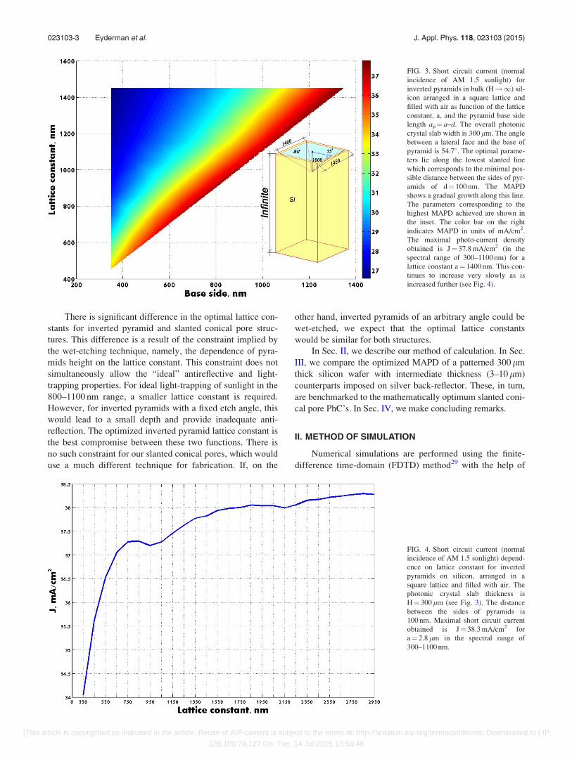
FIG. 4. Short circuit current (normal
incidence of AM 1.5 sunlight) depend-
ence on lattice constant for inverted
pyramids on silicon, arranged in a
square lattice and filled with air. The
photonic crystal slab thickness is
H¼ 300 lm (see Fig. 3). The distance
between the sides of pyramids is
100 nm. Maximal short circuit current
obtained is J¼ 38.3 mA/cm2 for
a¼ 2.8 lm in the spectral range of
300–1100 nm.
023103-3 Eyderman et al. J. Appl. Phys. 118, 023103 (2015)
[This article is copyrighted as indicated in the article. Reuse of AIP content is subject to the terms at: http://scitation.aip.org/termsconditions. Downloaded to ] IP:
128.100.78.127 On: Tue, 14 Jul 2015 13:58:48
the Electromagnetic Template Library.30 We use a standard
scheme of the FDTD calculation in which propagation of a
wave impulse through the structure is modeled. During the
numerical experiment, the amplitudes of the reflected and
transmitted waves are recorded, transformed to the frequency
domain, and normalized by the incident spectrum. In this
way, we obtain directly the transmission T(x), reflection
R(x), and indirectly the absorption A(x)¼ 1�T(x)�R(x)
coefficients for given light frequency x, incident angle, and
polarization. The absorption coefficient is also independently
and directly evaluated using the formulae:
a x;~rð Þ ¼ x � ImðeÞj~Eðx;~rÞj2
c �ð
Re½~E0 � ~H�0 � � n̂dxdy
; A xð Þ ¼ð
d3~ra x;~rð Þ:
(1)
Here, x is an angular frequency, E is the electric field ampli-
tude calculated at each point of a computational grid located
within silicon, e is the frequency-dependent and complex
dielectric permittivity of silicon, E0 and H0 are electric and
magnetic vectors of the incident plane wave, n̂ is a normal
unit vector, and the superscript * indicates the complex con-
jugate. Both the direct and indirect methods for calculating
the absorption give identical results. However, when the
structure is imposed on a metallic substrate, the indirect
method of absorption simulation also includes absorption in
metal, which does not contribute to the MAPD. Therefore,
this approach leads to a slight overestimate of the MAPD. In
the present paper, we use an indirect method since it is less
time and resource consuming. The overestimation of the
MAPD does not exceed 0.6–0.8 mA/cm2 depending on the
geometry.
Experimental data on the silicon dielectric permittivity
is taken from Ref. 31. The frequency dependence e(x) is
assigned in the FDTD by considering a modified Lorentz
model where dielectric polarization depends both on the
electric field and its first time derivative.31 This model pro-
vides an accurate fit of the optical response of bulk crystal-
line silicon to sunlight over the wavelength range from 300
to 1100 nm, while conventional Debye, Drude, and Lorentz
approximations fail. Fitting of the silicon dielectric function
is found with the help of an open MATLAB program.32
The MAPD, in which all generated carriers are assumed
to be collected, is calculated by integrating the simulated
absorption with incident solar Air Mass 1.5 Global
Spectrum33 intensity I(k) over the required wavelength
range. Assuming that each absorbed photon is converted into
a single electron-hole pair that is separated across a P-N
junction and collected without recombination losses, we
obtain the maximum achievable short circuit current for AM
1.5 solar spectrum33 in the spectral window [kmin, kmax], all
collimated into normal incidence
J ¼ðkmax
kmin
ekhc
I kð ÞA kð Þdk: (2)
Here, I(k) is the incident AM 1.5 light intensity, A(k) is
the absorption coefficient obtained indirectly as A(x)¼ 1
�T(x)�R(x), h is Planck’s constant, e is the electronic
charge, and c is the speed of light.
III. MAXIMAL SHORT CIRCUIT CURRENTCALCULATION
The short circuit current is an alternative measure of the
total amount of AM 1.5 sunlight absorbed in a given struc-
ture. For 100% absorption of sunlight in the range of
300–1100 nm, the MAPD corresponds to 43.5 mA/cm2. For
reference purposes, we calculate the MAPD of a free-
standing (with air above and air below) bulk silicon slab
with the thickness of 300 lm. Calculating the absorption
coefficient and using formula (2) in the spectral range of
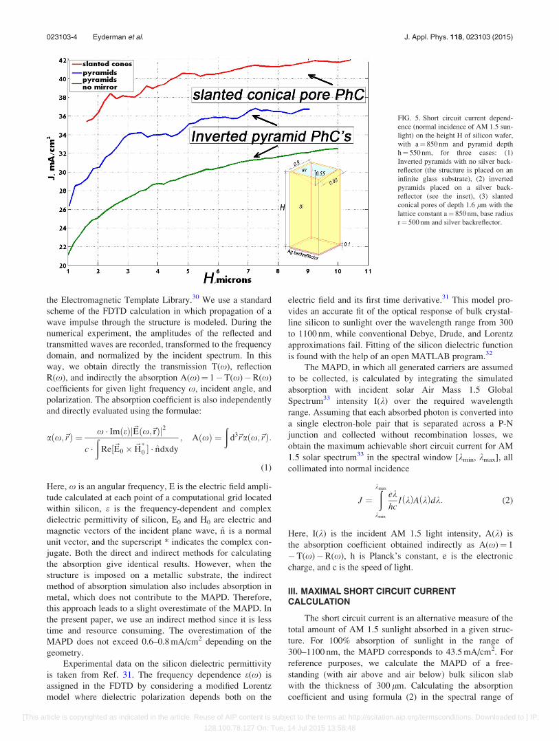
FIG. 5. Short circuit current depend-
ence (normal incidence of AM 1.5 sun-
light) on the height H of silicon wafer,
with a¼ 850 nm and pyramid depth
h¼ 550 nm, for three cases: (1)
Inverted pyramids with no silver back-
reflector (the structure is placed on an
infinite glass substrate), (2) inverted
pyramids placed on a silver back-
reflector (see the inset), (3) slanted
conical pores of depth 1.6 lm with the
lattice constant a¼ 850 nm, base radius
r¼ 500 nm and silver backreflector.
023103-4 Eyderman et al. J. Appl. Phys. 118, 023103 (2015)
[This article is copyrighted as indicated in the article. Reuse of AIP content is subject to the terms at: http://scitation.aip.org/termsconditions. Downloaded to ] IP:
128.100.78.127 On: Tue, 14 Jul 2015 13:58:48
300–1100 nm, we obtain the MAPD of J¼ 26.1 mA/cm2. In
other words, only 60% of the AM 1.5 sunlight in the
300–1100 nm is absorbed. This flat-cell architecture lacks
adequate light trapping and antireflective properties. We
now consider the effect of optimized periodic arrays of
inverted pyramids wet etched across the top surface for vari-
ous thicknesses of silicon wafers (Fig. 2).
In Fig. 3, we present a map for MAPD optimization
using an array of inverted pyramids in bulk (infinitely
thick) silicon arranged in a square lattice. Sunlight is
assumed collimated at normal incidence and the silicon
pores are filled with air (n¼ 1). The structure shown in the
inset of Fig. 3 provides a gradual increase of a MAPD with
increasing pyramid base side length. The optimal parame-
ters lie along the lowest slanted line which corresponds to
the minimal possible distance of 100 nm between the sides
of pyramids. We extend this region up to a¼ 3 lm (see
Fig. 4).
Fig. 4 shows that the MAPD growth saturates after the
lattice constant reaches 1.5 lm. When a¼ 1.5 lm and
h¼ 1.1 lm, the MAPD is close to 38 mA/cm2 in the
300–1100 nm wavelength range. This occurs for100 nm dis-
tance between pyramids bases and is almost 30% better than
the unpatterned silicon wafer reference case (with the
MAPD of only 26.1 mA/cm2). We find that the H¼ 300 lm
thick silicon wafer and the semi-infinite wafer (H!1) give
practically the same MAPD.
We examine the dependence of the MAPD on the silicon
wafer thickness for intermediate values of H¼ 3–10 lm
(Fig. 5). For this purpose, we fix the lattice constant
a¼ 850 nm (the optimal value found for the slanted conical
PhC), keeping the minimal possible distance between the
sides of pyramids equal d¼ 100 nm. For a¼ 850 nm, the
MAPD demonstrates a gradual increase with wafer thickness
but begins to saturate when the overall thickness H 5 lm.
We compare the MAPD dependence on the silicon wafer
thickness, H, for three cases: (1) with no silver back-reflector
(the PhC is placed on an infinite glass substrate), (2) with sil-
ver back-reflector (see Fig. 2b), and (3) mathematically opti-
mized slanted conical pore PhC with the lattice constant
a¼ 850 nm and base radius r¼ 500 nm,7 placed on a silver
back-reflector (Fig. 1).
For the specific choice of a¼ 850 nm, the slanted coni-
cal pore PhC (red curve) exhibits better performance than
wet-etched structure of the same overall height H by about
3–5 mA/cm2. We find a MAPD J¼ 35.5 mA/cm2 in the spec-
tral range of 300–1100 nm for H¼ h¼ 1.6 lm wafer thick-
ness, which corresponds just 1 lm effective bulk thickness of
silicon.7 As the thickness of slanted pore PhC is increased to
H¼ 10 lm (h remains equal 1.6 lm), the MAPD reaches
almost J¼ 42 mA/cm2, only slightly below the perfect solar
absorption value of 43.5 mA/cm2.
For the inverted pyramid PhC with lattice constant
a¼ 850 nm (Fig. 5 blue curve), when the overall height
H¼ 1.6 lm (1.43 lm equivalent bulk thickness) the MAPD
is about J¼ 29 mA/cm2. As the wafer thickness H increases,
the MAPD reaches almost J¼ 37 mA/cm2 at H¼ 9 lm. This
is just slightly below the MAPD for a 300 lm thick wafer
with the same lattice periodicity. For calibration purposes
and to delineate the role of the silver back-reflector, we also
calculate the dependence of the MAPD on H for an inverted
pyramid PhC’s (with a¼ 850 nm) sitting on a semi-infinite
glass substrate (green curve). In this case, the MAPD reaches
only J¼ 32.5 mA/cm2 for H¼ 10 lm.
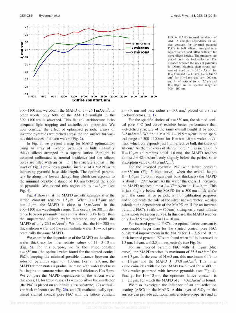
For inverted pyramid PhC’s, the optimal lattice constant is
considerably larger than for the slanted conical pore PhC.
Substantial improvements in the MAPD for H¼ 3, 5 and 10 lm
thick inverted pyramid PC’s are found when “a” is increased to
1.3 lm, 1.9 lm, and 2.5 lm, respectively (see Fig. 6).
For an inverted pyramid PhC with H¼ 3 lm (blue
curve), the MAPD reaches its maximum of 35.5 mA/cm2 for
a¼ 1.3 lm. In the case of H¼ 5 lm, this maximum shifts to
a¼ 1.9 lm and the MAPD J¼ 37.8 mA/cm2. This latter
value coincides with the best MAPD achieved for a 300 lm
thick wafer patterned with inverse pyramids (see Fig. 4).
Finally, for H¼ 10 lm, the optimum lattice constant is
a¼ 2.5 lm, for which the MAPD of J¼ 40 mA/cm2 is found.
We also investigate the influence of an anti-reflection
coating (ARC) on the MAPD. A thin layer of SiO2 on the
surface can provide additional antireflective properties and at
FIG. 6. MAPD (normal incidence of
AM 1.5 sunlight) dependence on lat-
tice constant for inverted pyramid
PhC’s in bulk silicon, arranged in a
square lattice, and filled with air for
three silicon heights. The structures are
placed on silver back-reflectors. The
distance between the sides of pyramids
is 100 nm. Maximal short circuit cur-
rent obtained is J¼ 35.5 mA/cm2 for
H¼ 3 lm and a¼ 1.3 lm, J¼ 37.8 mA/
cm2 for H¼ 5 lm and a¼ 1900 nm,
and J¼ 40 mA/cm2 for a¼ 2.5 lm and
H¼ 10 lm in the spectral range of
300–1100 nm.
023103-5 Eyderman et al. J. Appl. Phys. 118, 023103 (2015)
[This article is copyrighted as indicated in the article. Reuse of AIP content is subject to the terms at: http://scitation.aip.org/termsconditions. Downloaded to ] IP:
128.100.78.127 On: Tue, 14 Jul 2015 13:58:48
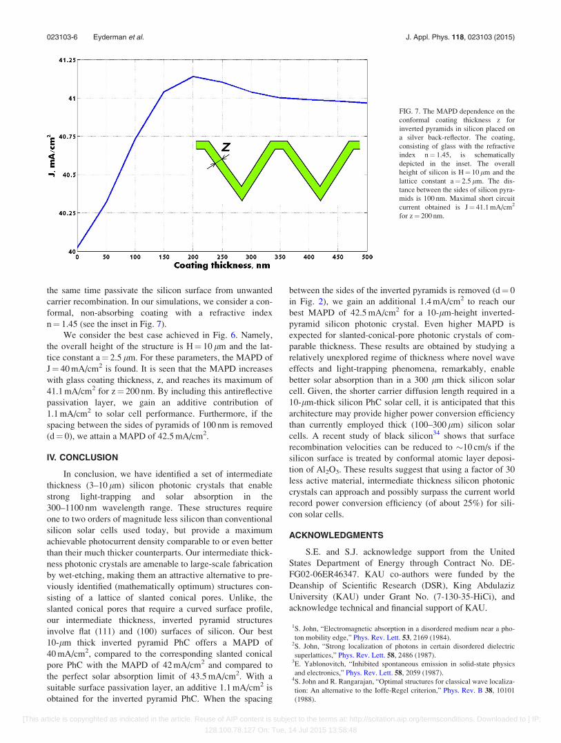
the same time passivate the silicon surface from unwanted
carrier recombination. In our simulations, we consider a con-
formal, non-absorbing coating with a refractive index
n¼ 1.45 (see the inset in Fig. 7).
We consider the best case achieved in Fig. 6. Namely,
the overall height of the structure is H¼ 10 lm and the lat-
tice constant a¼ 2.5 lm. For these parameters, the MAPD of
J¼ 40 mA/cm2 is found. It is seen that the MAPD increases
with glass coating thickness, z, and reaches its maximum of
41.1 mA/cm2 for z¼ 200 nm. By including this antireflective
passivation layer, we gain an additive contribution of
1.1 mA/cm2 to solar cell performance. Furthermore, if the
spacing between the sides of pyramids of 100 nm is removed
(d¼ 0), we attain a MAPD of 42.5 mA/cm2.
IV. CONCLUSION
In conclusion, we have identified a set of intermediate
thickness (3–10 lm) silicon photonic crystals that enable
strong light-trapping and solar absorption in the
300–1100 nm wavelength range. These structures require
one to two orders of magnitude less silicon than conventional
silicon solar cells used today, but provide a maximum
achievable photocurrent density comparable to or even better
than their much thicker counterparts. Our intermediate thick-
ness photonic crystals are amenable to large-scale fabrication
by wet-etching, making them an attractive alternative to pre-
viously identified (mathematically optimum) structures con-
sisting of a lattice of slanted conical pores. Unlike, the
slanted conical pores that require a curved surface profile,
our intermediate thickness, inverted pyramid structures
involve flat (111) and (100) surfaces of silicon. Our best
10-lm thick inverted pyramid PhC offers a MAPD of
40 mA/cm2, compared to the corresponding slanted conical
pore PhC with the MAPD of 42 mA/cm2 and compared to
the perfect solar absorption limit of 43.5 mA/cm2. With a
suitable surface passivation layer, an additive 1.1 mA/cm2 is
obtained for the inverted pyramid PhC. When the spacing
between the sides of the inverted pyramids is removed (d¼ 0
in Fig. 2), we gain an additional 1.4 mA/cm2 to reach our
best MAPD of 42.5 mA/cm2 for a 10-lm-height inverted-
pyramid silicon photonic crystal. Even higher MAPD is
expected for slanted-conical-pore photonic crystals of com-
parable thickness. These results are obtained by studying a
relatively unexplored regime of thickness where novel wave
effects and light-trapping phenomena, remarkably, enable
better solar absorption than in a 300 lm thick silicon solar
cell. Given, the shorter carrier diffusion length required in a
10-lm-thick silicon PhC solar cell, it is anticipated that this
architecture may provide higher power conversion efficiency
than currently employed thick (100–300 lm) silicon solar
cells. A recent study of black silicon34 shows that surface
recombination velocities can be reduced to �10 cm/s if the
silicon surface is treated by conformal atomic layer deposi-
tion of Al2O3. These results suggest that using a factor of 30
less active material, intermediate thickness silicon photonic
crystals can approach and possibly surpass the current world
record power conversion efficiency (of about 25%) for sili-
con solar cells.
ACKNOWLEDGMENTS
S.E. and S.J. acknowledge support from the United
States Department of Energy through Contract No. DE-
FG02-06ER46347. KAU co-authors were funded by the
Deanship of Scientific Research (DSR), King Abdulaziz
University (KAU) under Grant No. (7-130-35-HiCi), and
acknowledge technical and financial support of KAU.
1S. John, “Electromagnetic absorption in a disordered medium near a pho-
ton mobility edge,” Phys. Rev. Lett. 53, 2169 (1984).2S. John, “Strong localization of photons in certain disordered dielectric
superlattices,” Phys. Rev. Lett. 58, 2486 (1987).3E. Yablonovitch, “Inhibited spontaneous emission in solid-state physics
and electronics,” Phys. Rev. Lett. 58, 2059 (1987).4S. John and R. Rangarajan, “Optimal structures for classical wave localiza-
tion: An alternative to the Ioffe-Regel criterion,” Phys. Rev. B 38, 10101
(1988).
FIG. 7. The MAPD dependence on the
conformal coating thickness z for
inverted pyramids in silicon placed on
a silver back-reflector. The coating,
consisting of glass with the refractive
index n¼ 1.45, is schematically
depicted in the inset. The overall
height of silicon is H¼ 10 lm and the
lattice constant a¼ 2.5 lm. The dis-
tance between the sides of silicon pyra-
mids is 100 nm. Maximal short circuit
current obtained is J¼ 41.1 mA/cm2
for z¼ 200 nm.
023103-6 Eyderman et al. J. Appl. Phys. 118, 023103 (2015)
[This article is copyrighted as indicated in the article. Reuse of AIP content is subject to the terms at: http://scitation.aip.org/termsconditions. Downloaded to ] IP:
128.100.78.127 On: Tue, 14 Jul 2015 13:58:48
5A. Chutinan and S. John, “Light trapping and absorption optimization in
certain thin-film photonic crystal architectures,” Phys. Rev. A 78, 023825
(2008).6G. Demesy and S. John, “Solar energy trapping with modulated silicon
nanowire photonic crystals,” J. Appl. Phys. 112, 074326 (2012).7S. Eyderman, S. John, and A. Deinega, “Solar light trapping in slanted
conical-pore photonic crystals: Beyond statistical ray trapping,” J. Appl.
Phys. 113, 154315 (2013).8S. Eyderman, A. Deinega, and S. John, “Near perfect solar absorption in
ultra-thin-film GaAs photonic crystals,” J. Mater. Chem. A 2, 761–769
(2014).9A. Deinega and S. John, “Solar power conversion efficiency in modulated
silicon nanowire photonic crystals,” J. Appl. Phys. 112, 074327 (2012).10A. Deinega, S. Eyderman, and S. John, “Coupled optical and electrical
modeling of solar cell based on conical pore silicon photonic crystals,”
J. Appl. Phys. 113, 224501 (2013).11X. Zhang and A. Hosseini, “Polymer-based hybrid integrated photonic
devices for silicon on-chip modulation and board-level optical inter-
connects,” IEEE J. Sel. Top. Quantum Electron. 19(6), 3401115 (2013).12J. Yu et al., “Characterization and application of chirped photonic crystal
fiber in multiphoton imaging,” Opt. Express 22(9), 10366–10379 (2014).13X. Zhang et al., “Integrated photonic electromagnetic field sensor based
on broadband bowtie antenna coupled silicon organic hybrid modulator,”
IEEE J. Lightwave Technol. 32(20), 3774–3784 (2014).14A. Al-Rashid and S. John, “Optical bio-sensing of multiple disease
markers in a photonic-band-gap lab-on-a-chip: A conceptual paradigm,”
Phys. Rev. Appl. 3, 034001 (2015).15T. Saga, “Advances in crystalline silicon solar cell technology for indus-
trial mass production,” NPG Asia Mater. 2(3), 96 (2010).16M. A. Green, “The path to 25% silicon solar cell efficiency: History of sili-
con cell evolution,” Prog. Photovoltaics: Res. Appl. 17, 183–189 (2009).17P. Campbell and M. Green, “Light trapping properties of pyramidally tex-
tured surfaces,” J. Appl. Phys. 62, 243–249 (1987).18F.-J. Haug et al., “Resonances and absorption enhancement in thin film sil-
icon solar cells with periodic interface texture,” J. Appl. Phys. 109,
084516 (2011).19A. Deinega, I. Valuev, B. Potapkin, and Yu. Lozovik, “Minimizing light
reflection from dielectric textured surfaces,” JOSA A 28, 770–777 (2011).
20P. Bermel, C. Luo, L. Zeng, L. C. Kimerling, and J. D. Joannopoulos,
“Improving thin-film crystalline silicon solar cell efficiencies with pho-
tonic crystals,” Opt. Express 15(25), 16986 (2007).21J. Gjessing et al., “Comparison of periodic light-trapping structures in thin
crystalline silicon solar cells,” J. Appl. Phys. 110, 033104 (2011).22E. Garnett and P. Yang, “Light trapping in silicon nanowire solar cells,”
Nano Lett. 10(3), 1082–1087 (2010).23P. Kuang, A. Deinega, M.-L. Hsieh, S. John, and S.-Y. Lin, “Light trap-
ping and near-unity solar absorption in a three-dimensional photonic-
crystal,” Opt. Lett. 38(20), 4200 (2013).24X. Sheng, L. Z. Broderick, and L. C. Kimerling, “Photonic crystal struc-
tures for light trapping in thin-film Si solar cells: Modeling, process and
optimizations,” Opt. Commun. 314, 41–47 (2014).25X. H. Li et al., “Light trapping in thin-film solar cells via scattering by
nanostructured antireflection coatings,” J. Appl. Phys. 114, 044310 (2013).26X. Li, et al., “Subwavelength nanostructures integrated with polymer-
packaged III–V solar cells for omnidirectional, broad-spectrum improve-
ment of photovoltaic performance,” Prog. Photovoltaics: Res. Appl.
(published online).27H.-H. Lin and W.-H. Chen, “Improvement of polycrystalline silicon wafer
solar cell efficiency by forming nanoscale pyramids on wafer surface using
a self-mask etching technique,” J. Vac. Sci. Technol., B 31(3), 031401
(2013).28T. Deng, J. Chen, C. N. Wu, and Z. W. Liu, “Fabrication of inverted-
pyramid silicon nanopore arrays with three-step wet etching,” ECS J.
Solid State Sci. Technol. 2(11), 419–422 (2013).29A. Taflove and S. C. Hagness, Computational Electrodynamics: The
Finite-Difference Time-Domain Method, 3rd ed. (Artech House
Publishers, 2005).30See http://fdtd.kintechlab.com for Electromagnetic Template Library
(EMTL), Kintech Lab Ltd.31A. Deinega and S. John, “Effective optical response of silicon to sunlight
in the finite-difference time-domain method,” Opt. Lett. 37, 112 (2012).32See http://fdtd.kintechlab.com/en/fitting for Fitting of dielectric function.33See http://rredc.nrel.gov/solar/spectra/am1.5/ for Reference Solar Spectral
Irradiance: Air Mass 1.5.34H. Savin et al., “Black silicon solar cells with interdigitated back-contacts
achieve 22.1% efficiency,” Nat. Nanotechnol. 10, 624–628 (2015).
023103-7 Eyderman et al. J. Appl. Phys. 118, 023103 (2015)
[This article is copyrighted as indicated in the article. Reuse of AIP content is subject to the terms at: http://scitation.aip.org/termsconditions. Downloaded to ] IP:
128.100.78.127 On: Tue, 14 Jul 2015 13:58:48