Embed Size (px)
Citation preview
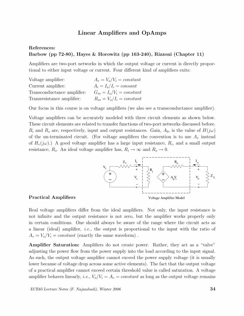
Linear Amplifiers and OpAmps
References:
Barbow (pp 72-80), Hayes & Horowitz (pp 163-240), Rizzoni (Chapter 11)
Amplifiers are two-port networks in which the output voltage or current is directly propor-
tional to either input voltage or current. Four different kind of amplifiers exits:
Voltage amplifier: Av = Vo/Vi = constant
Current amplifier: Ai = Io/Ii = consant
Transconductance amplifier: Gm = Io/Vi = constant
Transresistance amplifier: Rm = Vo/Ii = constant
Our focus in this course is on voltage amplifiers (we also see a transconductance amplifier).
Voltage amplifiers can be accurately modeled with three circuit elements as shown below.
These circuit elements are related to transfer functions of two-port networks discussed before.
Ri and Ro are, respectively, input and output resistances. Gain, A0, is the value of H(jω)
of the un-terminated circuit. (For voltage amplifiers the convention is to use Av instead
of Hv(jω).) A good voltage amplifier has a large input resistance, Ri, and a small output
resistance, Ro. An ideal voltage amplifier has, Ri → ∞ and Ro → 0.
+− V L
oI
o
+
−i
I
V
+
−iA V0
o
i
is
s
Voltage Amplifier Model
Z+−
VZ R
R
Practical Amplifiers
Real voltage amplifiers differ from the ideal amplifiers. Not only, the input resistance is
not infinite and the output resistance is not zero, but the amplifier works properly only
in certain conditions. One should always be aware of the range where the circuit acts as
a linear (ideal) amplifier, i.e., the output is proportional to the input with the ratio of
Av = Vo/Vi = constant (exactly the same waveform) .
Amplifier Saturation: Amplifiers do not create power. Rather, they act as a “valve”
adjusting the power flow from the power supply into the load according to the input signal.
As such, the output voltage amplifier cannot exceed the power supply voltage (it is usually
lower because of voltage drop across some active elements). The fact that the output voltage
of a practical amplifier cannot exceed certain threshold value is called saturation. A voltage
amplifier behaves linearly, i.e., Vo/Vi = Av = constant as long as the output voltage remains
ECE65 Lecture Notes (F. Najmabadi), Winter 2006 34
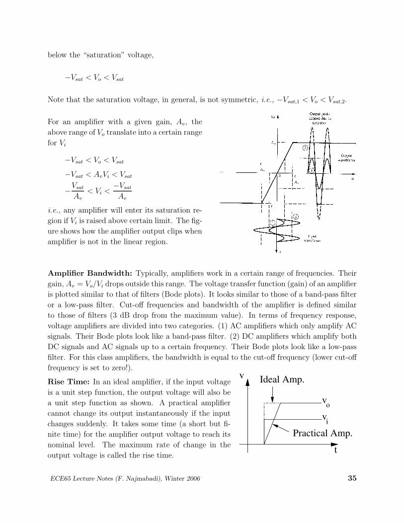
below the “saturation” voltage,
−Vsat < Vo < Vsat
Note that the saturation voltage, in general, is not symmetric, i.e., −Vsat,1 < Vo < Vsat,2.
For an amplifier with a given gain, Av, the
above range of Vo translate into a certain range
for Vi
−Vsat < Vo < Vsat
−Vsat < AvVi < Vsat
−Vsat
Av
< Vi <−Vsat
Av
i.e., any amplifier will enter its saturation re-
gion if Vi is raised above certain limit. The fig-
ure shows how the amplifier output clips when
amplifier is not in the linear region.
Amplifier Bandwidth: Typically, amplifiers work in a certain range of frequencies. Their
gain, Av = Vo/Vi drops outside this range. The voltage transfer function (gain) of an amplifier
is plotted similar to that of filters (Bode plots). It looks similar to those of a band-pass filter
or a low-pass filter. Cut-off frequencies and bandwidth of the amplifier is defined similar
to those of filters (3 dB drop from the maximum value). In terms of frequency response,
voltage amplifiers are divided into two categories. (1) AC amplifiers which only amplify AC
signals. Their Bode plots look like a band-pass filter. (2) DC amplifiers which amplify both
DC signals and AC signals up to a certain frequency. Their Bode plots look like a low-pass
filter. For this class amplifiers, the bandwidth is equal to the cut-off frequency (lower cut-off
frequency is set to zero!).
t
vv
i
o
v Ideal Amp.
Practical Amp.
Rise Time: In an ideal amplifier, if the input voltage
is a unit step function, the output voltage will also be
a unit step function as shown. A practical amplifier
cannot change its output instantaneously if the input
changes suddenly. It takes some time (a short but fi-
nite time) for the amplifier output voltage to reach its
nominal level. The maximum rate of change in the
output voltage is called the rise time.
ECE65 Lecture Notes (F. Najmabadi), Winter 2006 35
Maximum Output Current: A voltage amplifier model includes a controlled voltage
source in its output circuit. This means that for a given input signal, this controlled source
will have a fixed voltage independent of the current drawn from it. If we attach a load to
the circuit and start reducing the load resistance, the output voltage remains a constant and
load current will increase. Following this model, one could reduce the load resistance to a
very small value and draw a very large current from the amplifier.
In reality, this does not happen. Each voltage amplifier has a limited capability in providing
output current. This maximum output current limit is also called the “Short-Circuit Output
Current,” ISC. If one tries to exceed this current limit, the voltage amplifier will not behave
linearly; the output current will not increase, rather the current stays constant and the
output voltage and the gain will decrease.
I−
SC ≤ Io ≤ I+
SC
If the a fixed load resistance, RL, is connected to the amplifier, the maximum output current
means that the output voltage cannot exceed the RLISC :
RLI−
SC ≤ vo ≤ RLI+
SC
In this case, the maximum output current limit manifests itself in a form similar to amplifier
saturation. The output voltage waveform will be clipped at value of RLISC. Two options are
available to avoid the maximum current limit: (1) Increasing RL as is seen from the above
equation, (2) decreasing vo by decreasing the input amplitude.
There are other limitations of a practical amplifier such as signal-to-noise ratio, nonlinear
distortion, etc. which are out of the scope of this course.
How to measure Av, Ri, Ro
Measuring Av is straight forward. Apply a sinusoidal input signal with amplitude Vi to the
input, measure the amplitude of the input and output signals with a very large load (scope
input resistance). Make sure that the amplifier is not in saturation and signal is not clipped),
and compute Av = Vo/Vi. Note that Av is in general depends on frequency. There may also
been some phase difference between Vi and Vo similar to filters.
Measuring input and output resistances (or impedances) is not trivial. Part of the difficulty
is due to the fact that an Am-meter is limited to 60 Hz (good one can measure up to a few
kHz) and we should use scopes that only measure voltages. In order to measure a current
with scope, we need to find the voltage across a resistor whose value is accurately known.
ECE65 Lecture Notes (F. Najmabadi), Winter 2006 36
Care should be taken as addition of such a resistor to the circuit may modify its behavior.
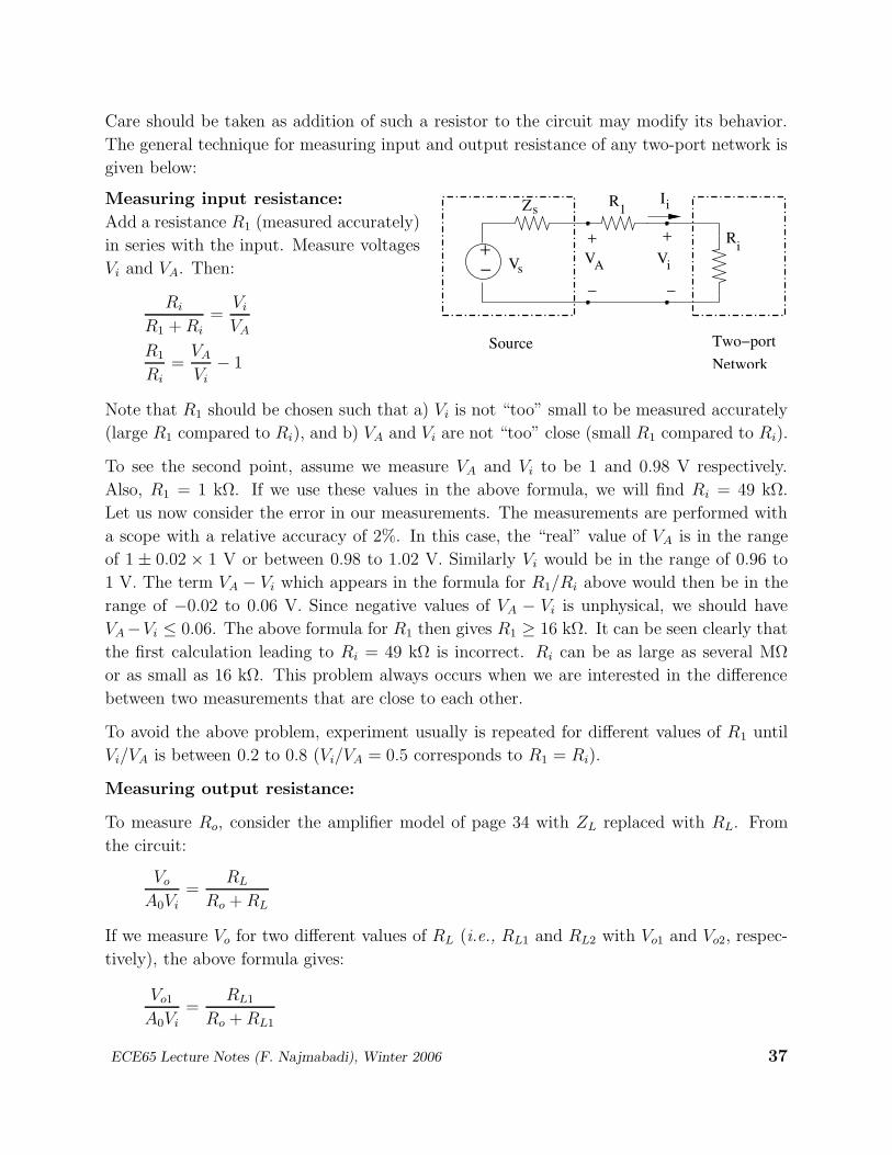
The general technique for measuring input and output resistance of any two-port network is
given below:
s
sVA Vi
i
Ii
−
+
1
+
−
NetworkTwo−portSource
Z
−+
VR
RMeasuring input resistance:
Add a resistance R1 (measured accurately)
in series with the input. Measure voltages
Vi and VA. Then:
Ri
R1 + Ri
=Vi
VA
R1
Ri
=VA
Vi
− 1
Note that R1 should be chosen such that a) Vi is not “too” small to be measured accurately
(large R1 compared to Ri), and b) VA and Vi are not “too” close (small R1 compared to Ri).
To see the second point, assume we measure VA and Vi to be 1 and 0.98 V respectively.
Also, R1 = 1 kΩ. If we use these values in the above formula, we will find Ri = 49 kΩ.
Let us now consider the error in our measurements. The measurements are performed with
a scope with a relative accuracy of 2%. In this case, the “real” value of VA is in the range
of 1 ± 0.02 × 1 V or between 0.98 to 1.02 V. Similarly Vi would be in the range of 0.96 to
1 V. The term VA − Vi which appears in the formula for R1/Ri above would then be in the
range of −0.02 to 0.06 V. Since negative values of VA − Vi is unphysical, we should have
VA−Vi ≤ 0.06. The above formula for R1 then gives R1 ≥ 16 kΩ. It can be seen clearly that
the first calculation leading to Ri = 49 kΩ is incorrect. Ri can be as large as several MΩ
or as small as 16 kΩ. This problem always occurs when we are interested in the difference
between two measurements that are close to each other.
To avoid the above problem, experiment usually is repeated for different values of R1 until
Vi/VA is between 0.2 to 0.8 (Vi/VA = 0.5 corresponds to R1 = Ri).
Measuring output resistance:
To measure Ro, consider the amplifier model of page 34 with ZL replaced with RL. From
the circuit:
Vo
A0Vi
=RL
Ro + RL
If we measure Vo for two different values of RL (i.e., RL1 and RL2 with Vo1 and Vo2, respec-
tively), the above formula gives:
Vo1
A0Vi
=RL1
Ro + RL1
ECE65 Lecture Notes (F. Najmabadi), Winter 2006 37
Vo2
A0Vi
=RL2
Ro + RL2
If the two measurements are done for the same value Vi, dividing the two equations give:
Vo1
Vo2
=RL1
Ro + RL1
× Ro + RL2
RL2
which can be solved to find Ro. Typically, we choose RL2 to be very large, RL2 → ∞ (e.g.,
internal resistance of scope). Call Vo2 = Voc (open circuit voltage). Then:
Vo1
Voc
=RL1
Ro + RL1
Ro
RL1
=Voc
Vo1
− 1
We also note:
Vo2 = AVi = Voc → A =Voc
Vi
So, this measurement will give both gain and output resistance.
Similar to measuring the input resistance, we should choose RL1 such that Vo1 is sufficiently
different from Voc for the measurement to be accurate. As in the case of measuring in-
put resistance, several values of RL1 are used until Vo1/Voc is typically between 0.2 to 0.8
(Vo1/Voc = 0.5 corresponds to RL1 = Ro).
In some cases, we cannot reduce RL1 to a low enough level such that Voc/Vo1 is sufficiently
different from 1. This is due to the maximum output current limitation (we will revisit this
for OpAmps). In such cases, we cannot find the value of the output resistance. However,
we can still find a “bound” for Ro (similar to error analysis for input resistance that gave a
“bound” for the input resistance). Suppose RL1 is the “smallest” resistance that we can use
and at this value of RL1 and to accuracy of our scope (ε = 2%), Voc ≈ Vo.
If the relative measurement error is ε, then:
Vo1|measured (1 − ε) ≤ Vo1|real ≤ Vo1|measured (1 + ε)
Voc|measured (1 − ε) ≤ Voc|real ≤ Voc|measured (1 + ε)
1 − 2ε ≤ Voc
Vo1
∣
∣
∣
∣
real
≤ 1 + 2ε
Ro1
RL1
≤ 2ε → Ro ≤ 2εRL1
ECE65 Lecture Notes (F. Najmabadi), Winter 2006 38
So, for example, if the accuracy of the scope is 2% and the minimum RL1 we could use was
1 kΩ, the bound for Ro ≤ 2 × 0.02 × 1000 = 40 Ω.
Feedback
Not only a good amplifier should have sufficient gain, its performance should be insensitive to
environmental and manufacturing conditions, should have a large Ri, a small Ro, a sufficiently
large bandwidth, etc. It is easy to make an amplifier with a very large gain. A typical
transistor circuit can easily have a gain of 100 or more. A three-stage transistor amplifier
can easily get gains of 106. Other characteristics of a good amplifier is hard to achieve. For
example, the β of a BJT changes with operating temperature making the gain of the three-
stage amplifier vary widely. The system can be made to be insensitive to environmental and
manufacturing conditions by the use of feedback. Feedback also helps in other regards.
Principle of feedback: The input to the circuit is modified by “feeding” a signal propor-
tional to the output value “back” to the input. There are two types of feedback (remember
the example of a car in the freeway discussed in the class):
1. Negative feedback: As the output is increased, the input signal is decreased and vice
versa. Negative feedback stabilizes the output to the desired level. Linear system employs
negative feedback.
2. Positive feedback: As the output is increased, the input signal is increased and vice
versa. Positive feedback leads to instability. (But, it has its uses!)
We will explore the concept of feedback in the context of operational amplifiers.
ECE65 Lecture Notes (F. Najmabadi), Winter 2006 39
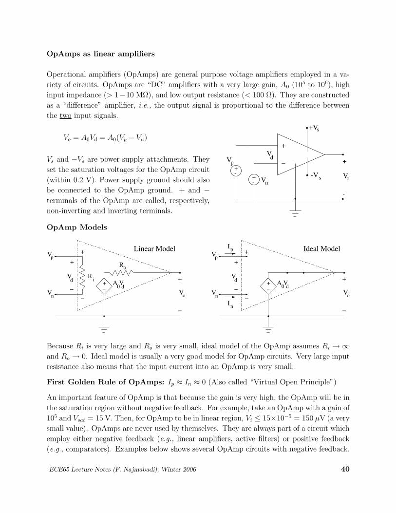
OpAmps as linear amplifiers
Operational amplifiers (OpAmps) are general purpose voltage amplifiers employed in a va-
riety of circuits. OpAmps are “DC” amplifiers with a very large gain, A0 (105 to 106), high
input impedance (> 1−10 MΩ), and low output resistance (< 100 Ω). They are constructed
as a “difference” amplifier, i.e., the output signal is proportional to the difference between
the two input signals.
+-
+-
-Vs
+Vs
+
-
Vn
VpVd
Vo
+
_
Vo = A0Vd = A0(Vp − Vn)
Vs and −Vs are power supply attachments. They
set the saturation voltages for the OpAmp circuit
(within 0.2 V). Power supply ground should also
be connected to the OpAmp ground. + and −terminals of the OpAmp are called, respectively,
non-inverting and inverting terminals.
OpAmp Models
Linear Model
−+
o
+
+
−
−
d
+
−
p
n
o
id0
R
V
V
V V
R
A V
p
n
−+
o
+
+
−
−
d
+
−
p
n
Ideal Model
d0
I
I
V
V
V VA V
Because Ri is very large and Ro is very small, ideal model of the OpAmp assumes Ri → ∞and Ro → 0. Ideal model is usually a very good model for OpAmp circuits. Very large input
resistance also means that the input current into an OpAmp is very small:
First Golden Rule of OpAmps: Ip ≈ In ≈ 0 (Also called “Virtual Open Principle”)
An important feature of OpAmp is that because the gain is very high, the OpAmp will be in
the saturation region without negative feedback. For example, take an OpAmp with a gain of
105 and Vsat = 15 V. Then, for OpAmp to be in linear region, Vi ≤ 15×10−5 = 150 µV (a very
small value). OpAmps are never used by themselves. They are always part of a circuit which
employ either negative feedback (e.g., linear amplifiers, active filters) or positive feedback
(e.g., comparators). Examples below shows several OpAmp circuits with negative feedback.
ECE65 Lecture Notes (F. Najmabadi), Winter 2006 40
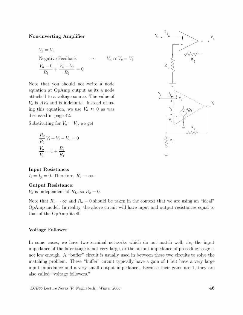
Inverting Amplifier
i
i oL
1
2
I
V VR
R
+−
R
+
−
i 1
d−+
+
−
2
o
1
L
n
n
p
−
++
−
d0
V R
V
VV
V
R
I
I
R
A V
The first step in solving OpAmp circuits is to replace the OpAmp with its circuit model
(ideal model is usually very good).
Vp = 0, Vo = A0Vd = A0(Vp − Vn) = −A0Vn
Using node-voltage method and noting In ≈ 0:
Vn − Vi
R1
+Vn − Vo
R2
= 0
Substituting for Vn = −Vo/A0 and multiplying the equation by R2, we have:
− R2
A0R1
Vo −R2
R1
Vi −Vo
A0
− Vo = 0 → Vo
[
1 +1
A0
+R2
A0R1
]
= −R2
R1
Vi
Vo
Vi
= − R2
R1
1
1 +1
A0
+R2
A0R1
Since OpAmp gain is very large, 1/A0 1. Also if R2 and R1 are chosen such that their
ratio is not very large, R2/R1 A0 or R2/(A0R1) 1, then the voltage transfer function
of the OpAmp is
Vo
Vi
= − R2
R1
The circuit is called an inverting amplifier because the voltage transfer function is “negative.”
(A “negative” sinusoidal function looks inverted.) The negative sign means that there is 180
phase shift between input and output signals.
ECE65 Lecture Notes (F. Najmabadi), Winter 2006 41
Note that the voltage transfer function is “independent” of the OpAmp gain, A0, and is only
set by the values of the resistors R1 and R2. While A0 is quite sensitive to environmental and
manufacturing conditions (can very by a factor of 10 to 100), the resistor values are quite
insensitive and, thus, the gain of the system is quite stable. This stability is achieved by
negative feedback, the output of the OpAmp is connected via R2 to the inverting terminal
of OpAmp. If Vo increases, this resistor forces Vn to increase, reducing Vd = Vp − Vn and
Vo = A0Vd, and stabilizes the OpAmp output.
An important feature of OpAmp circuits with negative feedback is that because the OpAmp
is NOT saturated, Vd = Vo/A0 is very small (because A0 is very large). As a result,
Negative Feedback → Vd ≈ 0 → Vn ≈ Vp
Second Golden Rule of OpAmps: For OpAmps circuits with negative feedback, the
OpAmp adjusts its output voltage such that Vd ≈ 0 or Vn ≈ Vp (also called “Virtual Short
Principle”). This rule is derived by assuming A → ∞. Thus, Vo cannot be found from
Vo = A0vd = ∞ × 0 = indefinite value. The virtual short principle replace Vo = A0vd
expression with Vd ≈ 0.
The above rule simplifies solution to OpAmp circuits dramatically. For example, for the
inverting amplifier circuit above, we will have:
Negative Feedback → Vn ≈ Vp ≈ 0
Vn − Vi
R1
+Vn − Vo
R2
= 0 → Vi
R1
+Vo
R2
= 0 → Vo
Vi
= − R2
R1
Input and Output resistances of inverting amplifier configuration: From the circuit,
Ii =Vi − 0
R1
→ Ri =Vi
Ii
= R1
The input impedance of the inverting amplifier circuit is R1 (although input impedance of
OpAmp is infinite).
The output impedance of the circuit is “zero” because Vo is independent of RL (Vo does not
change when RL is changed).
Amplifier Bandwidth:
The voltage gain for the inverting amplifier is −R2/R1 and is independent of frequency–same
gain for a DC signal (ω → 0) as for high frequencies. However, this voltage gain has been
found using an ideal OpAmp model (ideal OpAmp parameters are independent of frequency).
ECE65 Lecture Notes (F. Najmabadi), Winter 2006 42
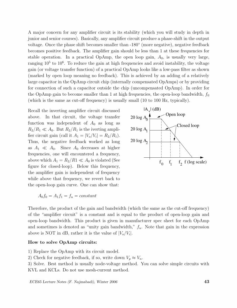
A major concern for any amplifier circuit is its stability (which you will study in depth in
junior and senior courses). Basically, any amplifier circuit produce a phase-shift in the output
voltage. Once the phase shift becomes smaller than -180 (more negative), negative feedback
becomes positive feedback. The amplifier gain should be less than 1 at these frequencies for
stable operation. In a practical OpAmp, the open loop gain, A0, is usually very large,
ranging 105 to 106. To reduce the gain at high frequencies and avoid instability, the voltage
gain (or voltage transfer function) of a practical OpAmp looks like a low-pass filter as shown
(marked by open loop meaning no feedback). This is achieved by an adding of a relatively
large capacitor in the OpAmp circuit chip (internally compensated OpAmps) or by providing
for connection of such a capacitor outside the chip (uncompensated OpAmp). In order for
the OpAmp gain to become smaller than 1 at high frequencies, the open-loop bandwidth, f0
(which is the same as cut-off frequency) is usually small (10 to 100 Hz, typically).
|A | (dB)v20 log A0
20 log A
20 log A
1
2
f f f0 1 2
Closed loop
Open loop
f (log scale)
Recall the inverting amplifier circuit discussed
above. In that circuit, the voltage transfer
function was independent of A0 as long as
R2/R1 A0. But R2/R1 is the iverting ampli-
fier circuit gain (call it A1 = |Vo/Vi| = R2/R1).
Thus, the negative feedback worked as long
as A1 A0. Since A0 decreases at higher
frequencies, one will encountered a frequency,
above which A1 = R2/R1 A0 is violated (See
figure for closed-loop). Below this frequency,
the amplifier gain is independent of frequency
while above that frequency, we revert back to
the open-loop gain curve. One can show that:
A0f0 = A1f1 = fu = constant
Therefore, the product of the gain and bandwidth (which the same as the cut-off frequency)
of the “amplifier circuit” is a constant and is equal to the product of open-loop gain and
open-loop bandwidth. This product is given in manufacturer spec sheet for each OpAmp
and sometimes is denoted as “unity gain bandwidth,” fu. Note that gain in the expression
above is NOT in dB, rather it is the value of |Vo/Vi|.
How to solve OpAmp circuits:
1) Replace the OpAmp with its circuit model.
2) Check for negative feedback, if so, write down Vp ≈ Vn.
3) Solve. Best method is usually node-voltage method. You can solve simple circuits with
KVL and KCLs. Do not use mesh-current method.
ECE65 Lecture Notes (F. Najmabadi), Winter 2006 43
Physical Limitations of OpAmps
OpAmps, like other voltage amplifiers, behave linearly only under certain conditions (see
page 34-35). Several limitations of OpAmp circuits are discussed before.
1. Voltage-supply limit or Saturation: v−
s < vo < v+s which limits the maximum
output voltage (or a for a given gain, limits the maximum input voltage). If an amplifier is
saturated, one can recover the linear regime by reducing the input amplitude.
2. Frequency Response limit: A practical amplifier has a finite bandwidth. For OpAmps
circuits with negative feedback, one can trade gain with bandwidth:
A0ω0 = Aω or A0f0 = Af = fu
Note that gain in the expression above is NOT in dB, rather it is the value of |Vo/Vi|.
3. Maximum output current limit: A practial voltage amplifier has a limited capability
in providing output current. This maximum output current limit is also called the “Short-
Circuit Output Current,” ISC . Thus, Io ≤ ISC. (see discussion of page 36).
Note: The maximum output current of the OpAmp amplifier configuration is NOT the
same as the maximum output current of the OpAmp itself. For example in the inverting
amplifier configuration, the maximum output current of the amplifier is smaller than ISC of
OpAmp because OpAmp has to supply current to both the load (maximum output current
of amplifier configuration itself) and the feedback resistor R2.
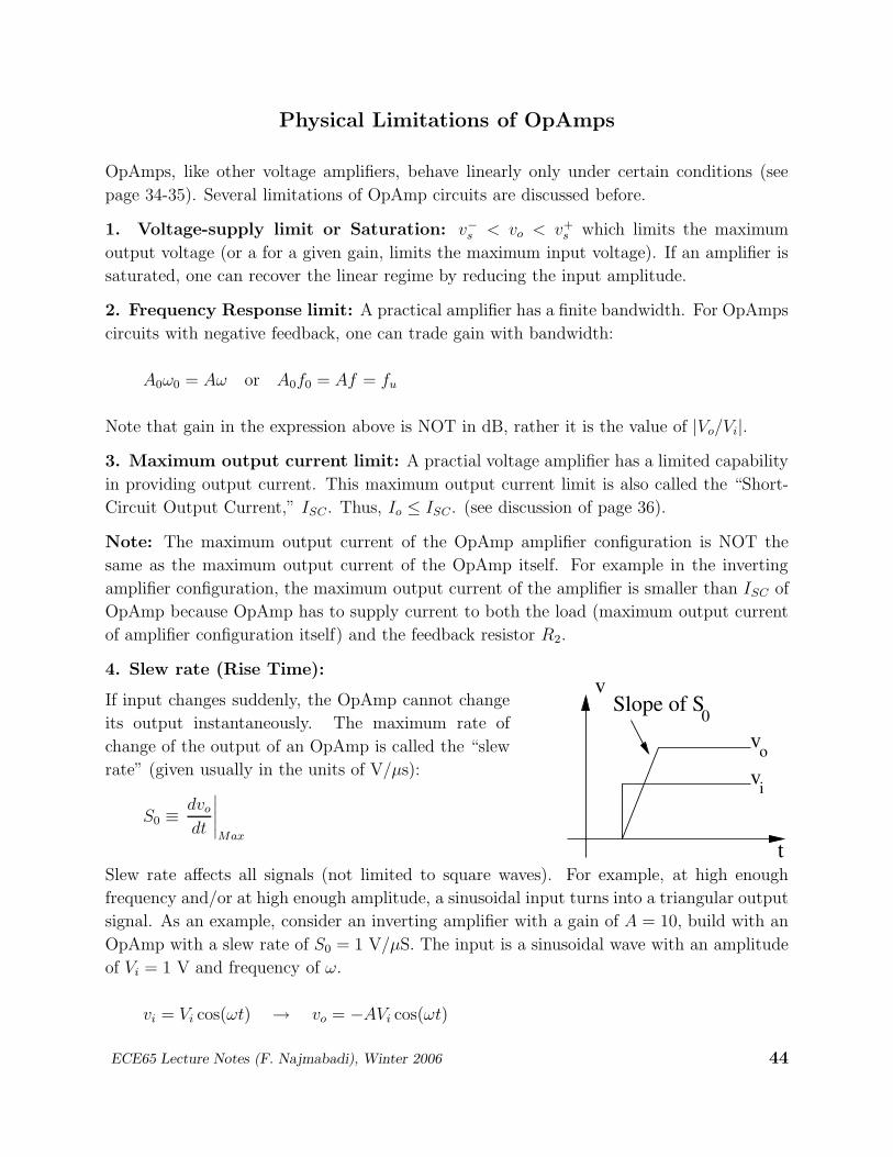
4. Slew rate (Rise Time):
0Slope of S
o
t
vv
v
i
If input changes suddenly, the OpAmp cannot change
its output instantaneously. The maximum rate of
change of the output of an OpAmp is called the “slew
rate” (given usually in the units of V/µs):
S0 ≡dvo
dt
∣
∣
∣
∣
∣
Max
Slew rate affects all signals (not limited to square waves). For example, at high enough
frequency and/or at high enough amplitude, a sinusoidal input turns into a triangular output
signal. As an example, consider an inverting amplifier with a gain of A = 10, build with an
OpAmp with a slew rate of S0 = 1 V/µS. The input is a sinusoidal wave with an amplitude
of Vi = 1 V and frequency of ω.
vi = Vi cos(ωt) → vo = −AVi cos(ωt)
ECE65 Lecture Notes (F. Najmabadi), Winter 2006 44
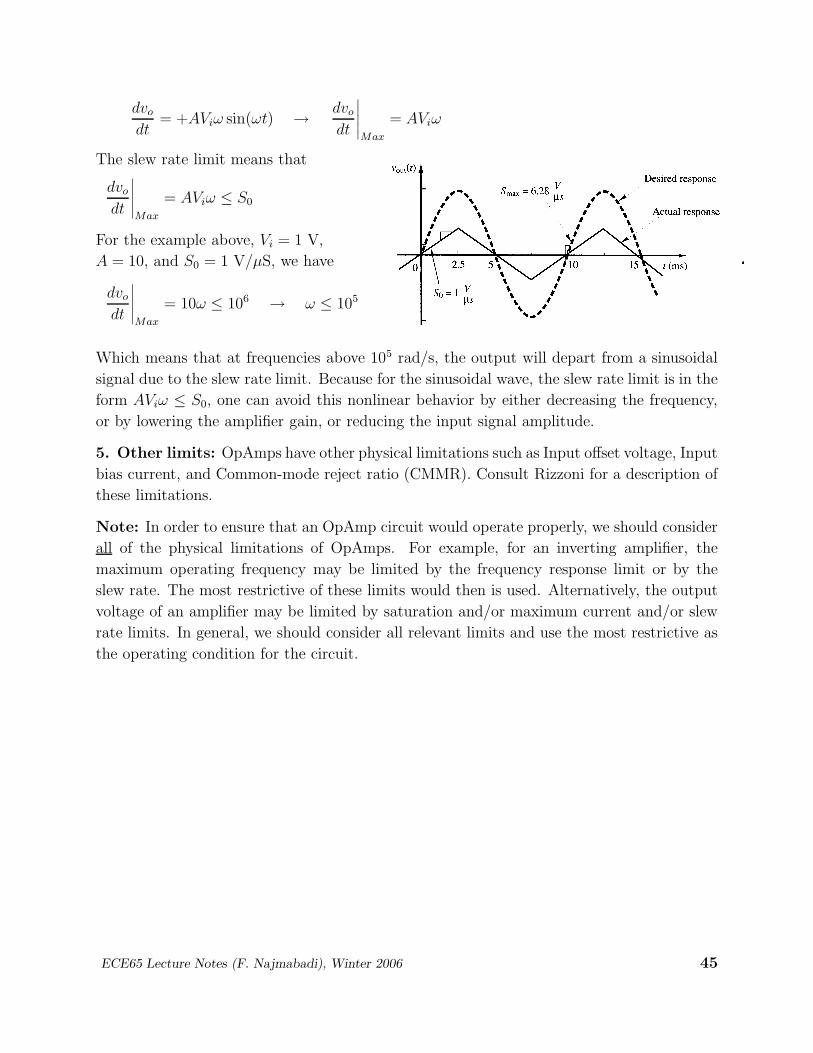
dvo
dt= +AViω sin(ωt) → dvo
dt
∣
∣
∣
∣
∣
Max
= AViω
The slew rate limit means that
dvo
dt
∣
∣
∣
∣
∣
Max
= AViω ≤ S0
For the example above, Vi = 1 V,
A = 10, and S0 = 1 V/µS, we have
dvo
dt
∣
∣
∣
∣
∣
Max
= 10ω ≤ 106 → ω ≤ 105
Which means that at frequencies above 105 rad/s, the output will depart from a sinusoidal
signal due to the slew rate limit. Because for the sinusoidal wave, the slew rate limit is in the
form AViω ≤ S0, one can avoid this nonlinear behavior by either decreasing the frequency,
or by lowering the amplifier gain, or reducing the input signal amplitude.
5. Other limits: OpAmps have other physical limitations such as Input offset voltage, Input
bias current, and Common-mode reject ratio (CMMR). Consult Rizzoni for a description of
these limitations.
Note: In order to ensure that an OpAmp circuit would operate properly, we should consider
all of the physical limitations of OpAmps. For example, for an inverting amplifier, the
maximum operating frequency may be limited by the frequency response limit or by the
slew rate. The most restrictive of these limits would then is used. Alternatively, the output
voltage of an amplifier may be limited by saturation and/or maximum current and/or slew
rate limits. In general, we should consider all relevant limits and use the most restrictive as
the operating condition for the circuit.
ECE65 Lecture Notes (F. Najmabadi), Winter 2006 45
1
2
ii
o
RR
VI
+-
V
i
o
2
1
+
−
d
+
− −+
n
p
p
d0
V
V
R
R
V
V
VI
A V
Non-inverting Amplifier
Vp = Vi
Negative Feedback → Vn ≈ Vp = Vi
Vn − 0
R1
+Vn − Vo
R2
= 0
Note that you should not write a node
equation at OpAmp output as its a node
attached to a voltage source. The value of
Vo is AVd and is indefinite. Instead of us-
ing this equation, we use Vd ≈ 0 as was
discussed in page 42.
Substituting for Vn = Vi, we get
R2
R1
Vi + Vi − Vo = 0
Vo
Vi
= 1 +R2
R1
Input Resistance:
Ii = Ip = 0. Therefore, Ri → ∞.
Output Resistance:
Vo is independent of RL, so Ro = 0.
Note that Ri → ∞ and Ro = 0 should be taken in the context that we are using an “ideal”
OpAmp model. In reality, the above circuit will have input and output resistances equal to
that of the OpAmp itself.
Voltage Follower
In some cases, we have two-terminal networks which do not match well, i.e, the input
impedance of the later stage is not very large, or the output impedance of preceding stage is
not low enough. A “buffer” circuit is usually used in between these two circuits to solve the
matching problem. These “buffer” circuit typically have a gain of 1 but have a very large
input impedance and a very small output impedance. Because their gains are 1, they are
also called “voltage followers.”
ECE65 Lecture Notes (F. Najmabadi), Winter 2006 46
i oV + V
−The non-inverting amplifier above has
Ri → ∞ and Ro = 0 and, therefore, can
be turned into a voltage follower (buffer)
by adjusting R1 and R2 such that the gain
is 1.
Vo
Vi
= 1 +R2
R1
= 1 → R2 = 0
So by setting R2 = 0, we have Vo = Vi or a gain of unity. We note that this expression is
valid for any value of R1. As we want to minimize the number of components in a circuit as
a rule (cheaper circuits!) we set R1 = ∞ (open circuit) and remove R1 from the circuit.
Inverting Summer
o1
2
f
1
2
p
n
−+ 0 d
VR
R
R
+−
V
V
V
V
A V
Vp = 0
Negative Feedback: Vn ≈ Vp = 0
Vn − V1
R1
+Vn − V2
R2
+Vn − Vo
Rf
= 0
Vo = −Rf
R1
V1 −Rf
R2
V2
So, this circuit adds (sums) two signals.
An example of the use of this circuit is to
add a DC offset to a sinusoidal signal.
o1
2
1
2
f
s
p +
−−+
n
d0
VR
R
V
V
R
R
V
V
A V
Non-Inverting Summer
Negative Feedback: Vn ≈ Vp
Vp − V1
R1
+Vp − V2
R2
= 0 −→
Vp
(
1
R1
+1
R2
)
=V1
R1
+V2
R2
Vn − 0
Rs
+Vn − Vo
Rf
= 0 −→
Vo =(
1 +Rf
Rs
)
Vn
ECE65 Lecture Notes (F. Najmabadi), Winter 2006 47
Substituting for Vn in the second equation from the first (noting Vp = Vn):
Vo =1 + Rf/Rs
1/R1 + 1/R2
(
V1
R1
+V2
R2
)
So, this circuit also signal adds (sums) two signals. It does not, however, inverts the signals.
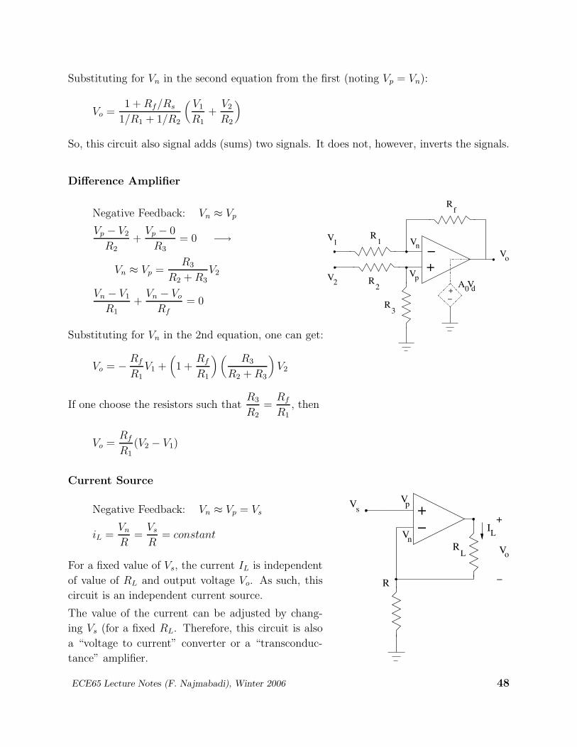
Difference Amplifier
o
1 1
2 2
f
p
n
−+
3
d0
VV R
V R
R
+−
V
V
R
A V
Negative Feedback: Vn ≈ Vp
Vp − V2
R2
+Vp − 0
R3
= 0 −→
Vn ≈ Vp =R3
R2 + R3
V2
Vn − V1
R1
+Vn − Vo
Rf
= 0
Substituting for Vn in the 2nd equation, one can get:
Vo = − Rf
R1
V1 +(
1 +Rf
R1
) (
R3
R2 + R3
)
V2
If one choose the resistors such thatR3
R2
=Rf
R1
, then
Vo =Rf
R1
(V2 − V1)
Current Source
L
L
s p
n
o
I
R
+−
V V
V
R
V
+
−
Negative Feedback: Vn ≈ Vp = Vs
iL =Vn
R=
Vs
R= constant
For a fixed value of Vs, the current IL is independent
of value of RL and output voltage Vo. As such, this
circuit is an independent current source.
The value of the current can be adjusted by chang-
ing Vs (for a fixed RL. Therefore, this circuit is also
a “voltage to current” converter or a “transconduc-
tance” amplifier.
ECE65 Lecture Notes (F. Najmabadi), Winter 2006 48
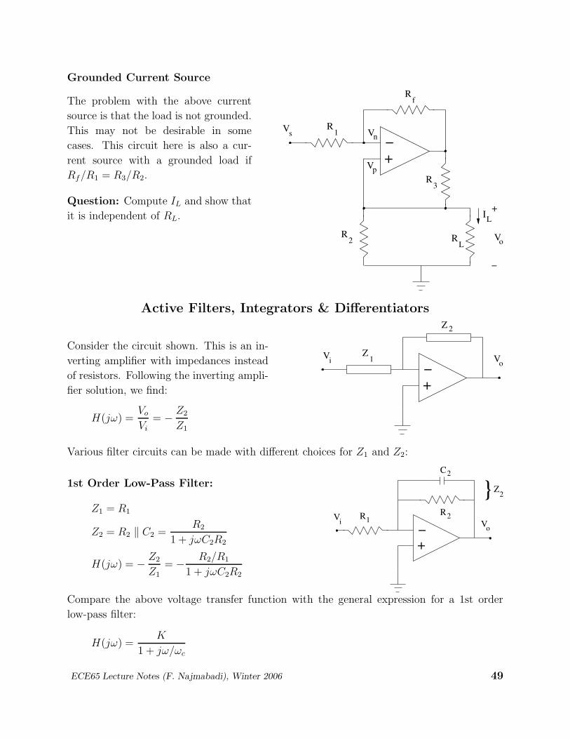
Grounded Current Source
1
3
2 L
s
f
n
p
L+
−
Vo
R
R
R R
V
R
V
V +−
I
The problem with the above current
source is that the load is not grounded.
This may not be desirable in some
cases. This circuit here is also a cur-
rent source with a grounded load if
Rf/R1 = R3/R2.
Question: Compute IL and show that
it is independent of RL.
Active Filters, Integrators & Differentiators
oi 1
2
VV
+−
Z
Z
Consider the circuit shown. This is an in-
verting amplifier with impedances instead
of resistors. Following the inverting ampli-
fier solution, we find:
H(jω) =Vo
Vi
= − Z2
Z1
Various filter circuits can be made with different choices for Z1 and Z2:
2
2
2
1o
i
C
R
Z
RV
V
+−
1st Order Low-Pass Filter:
Z1 = R1
Z2 = R2 ‖ C2 =R2
1 + jωC2R2
H(jω) = − Z2
Z1
= − R2/R1
1 + jωC2R2
Compare the above voltage transfer function with the general expression for a 1st order
low-pass filter:
H(jω) =K
1 + jω/ωc
ECE65 Lecture Notes (F. Najmabadi), Winter 2006 49
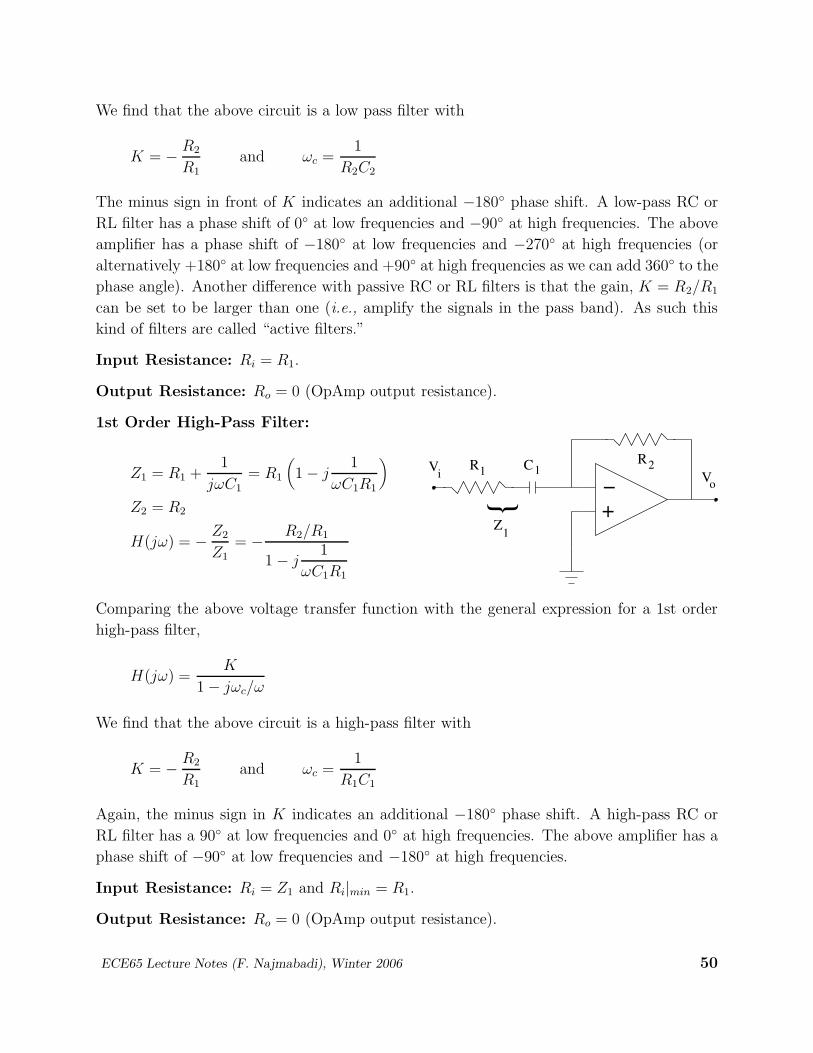
We find that the above circuit is a low pass filter with
K = − R2
R1
and ωc =1
R2C2
The minus sign in front of K indicates an additional −180 phase shift. A low-pass RC or
RL filter has a phase shift of 0 at low frequencies and −90 at high frequencies. The above
amplifier has a phase shift of −180 at low frequencies and −270 at high frequencies (or
alternatively +180 at low frequencies and +90 at high frequencies as we can add 360 to the
phase angle). Another difference with passive RC or RL filters is that the gain, K = R2/R1
can be set to be larger than one (i.e., amplify the signals in the pass band). As such this
kind of filters are called “active filters.”
Input Resistance: Ri = R1.
Output Resistance: Ro = 0 (OpAmp output resistance).
1st Order High-Pass Filter:
2o
i 1 1
1
RV
V R C
Z+−
Z1 = R1 +1
jωC1
= R1
(
1 − j1
ωC1R1
)
Z2 = R2
H(jω) = − Z2
Z1
= − R2/R1
1 − j1
ωC1R1
Comparing the above voltage transfer function with the general expression for a 1st order
high-pass filter,
H(jω) =K
1 − jωc/ω
We find that the above circuit is a high-pass filter with
K = − R2
R1
and ωc =1
R1C1
Again, the minus sign in K indicates an additional −180 phase shift. A high-pass RC or
RL filter has a 90 at low frequencies and 0 at high frequencies. The above amplifier has a
phase shift of −90 at low frequencies and −180 at high frequencies.
Input Resistance: Ri = Z1 and Ri|min = R1.
Output Resistance: Ro = 0 (OpAmp output resistance).
ECE65 Lecture Notes (F. Najmabadi), Winter 2006 50
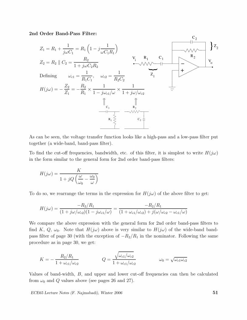
2nd Order Band-Pass Filter:
2
2
oi 1 1
2
1
R
Z
VV R C
C
Z+−
Z1 = R1 +1
jωC1
= R1
(
1 − j1
ωC1R1
)
Z2 = R2 ‖ C2 =R2
1 + jωC2R2
Defining ωc1 =1
R1C1
, ωc2 =1
R2C2
H(jω) = − Z2
Z1
= −R2
R1
× 1
1 − jωc1/ω× 1
1 + jω/ωc2~
w
w
~
w
w
1
1
2
2
C
R
R
C
As can be seen, the voltage transfer function looks like a high-pass and a low-pass filter put
together (a wide-band, band-pass filter).
To find the cut-off frequencies, bandwidth, etc. of this filter, it is simplest to write H(jω)
in the form similar to the general form for 2nd order band-pass filters:
H(jω) =K
1 + jQ(
ω
ω0
− ω0
ω
)
To do so, we rearrange the terms in the expression for H(jω) of the above filter to get:
H(jω) =−R2/R1
(1 + jω/ωc2)(1 − jωc1/ω)=
−R2/R1
(1 + ωc1/ωc2) + j(ω/ωc2 − ωc1/ω)
We compare the above expression with the general form for 2nd order band-pass filters to
find K, Q, ω0. Note that H(jω) above is very similar to H(jω) of the wide-band band-
pass filter of page 30 (with the exception of −R2/R1 in the nominator. Following the same
procedure as in page 30, we get:
K = − R2/R1
1 + ωc1/ωc2
Q =
√
ωc1/ωc2
1 + ωc1/ωc2
ω0 =√
ωc1ωc2
Values of band-width, B, and upper and lower cut-off frequencies can then be calculated
from ω0 and Q values above (see pages 26 and 27).
ECE65 Lecture Notes (F. Najmabadi), Winter 2006 51
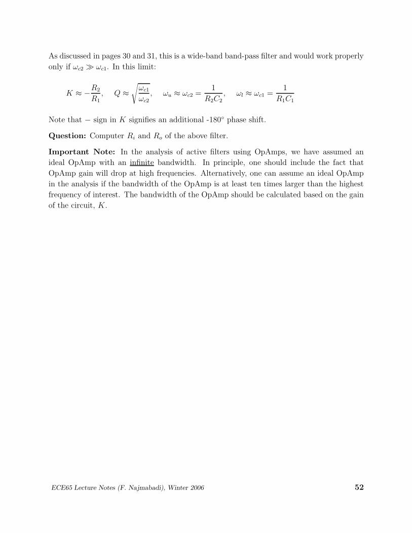
As discussed in pages 30 and 31, this is a wide-band band-pass filter and would work properly
only if ωc2 ωc1. In this limit:
K ≈ −R2
R1
, Q ≈√
ωc1
ωc2
, ωu ≈ ωc2 =1
R2C2
, ωl ≈ ωc1 =1
R1C1
Note that − sign in K signifies an additional -180 phase shift.
Question: Computer Ri and Ro of the above filter.
Important Note: In the analysis of active filters using OpAmps, we have assumed an
ideal OpAmp with an infinite bandwidth. In principle, one should include the fact that
OpAmp gain will drop at high frequencies. Alternatively, one can assume an ideal OpAmp
in the analysis if the bandwidth of the OpAmp is at least ten times larger than the highest
frequency of interest. The bandwidth of the OpAmp should be calculated based on the gain
of the circuit, K.
ECE65 Lecture Notes (F. Najmabadi), Winter 2006 52
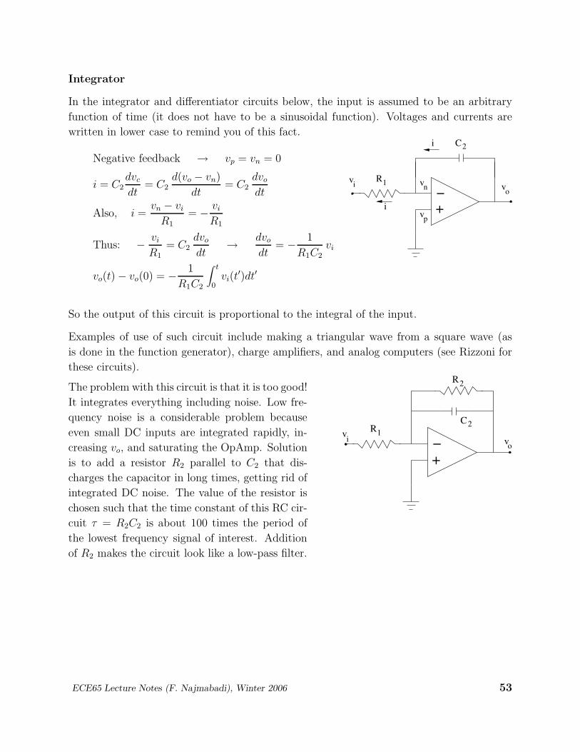
Integrator
In the integrator and differentiator circuits below, the input is assumed to be an arbitrary
function of time (it does not have to be a sinusoidal function). Voltages and currents are
written in lower case to remind you of this fact.
1
2
ion
p
i
i
R
C
+−
vvv
v
Negative feedback → vp = vn = 0
i = C2
dvc
dt= C2
d(vo − vn)
dt= C2
dvo
dt
Also, i =vn − vi
R1
= − vi
R1
Thus: − vi
R1
= C2
dvo
dt→ dvo
dt= − 1
R1C2
vi
vo(t) − vo(0) = − 1
R1C2
∫ t
0
vi(t′)dt′
So the output of this circuit is proportional to the integral of the input.
Examples of use of such circuit include making a triangular wave from a square wave (as
is done in the function generator), charge amplifiers, and analog computers (see Rizzoni for
these circuits).
12
2
io
RC
R
vv
+−
The problem with this circuit is that it is too good!
It integrates everything including noise. Low fre-
quency noise is a considerable problem because
even small DC inputs are integrated rapidly, in-
creasing vo, and saturating the OpAmp. Solution
is to add a resistor R2 parallel to C2 that dis-
charges the capacitor in long times, getting rid of
integrated DC noise. The value of the resistor is
chosen such that the time constant of this RC cir-
cuit τ = R2C2 is about 100 times the period of
the lowest frequency signal of interest. Addition
of R2 makes the circuit look like a low-pass filter.
ECE65 Lecture Notes (F. Najmabadi), Winter 2006 53
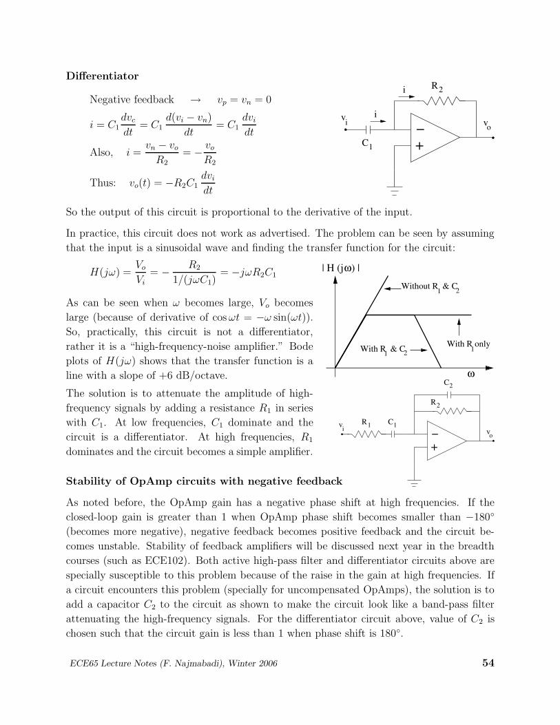
Differentiator
i
2
1
o
i
iv
R
C +− v
Negative feedback → vp = vn = 0
i = C1
dvc
dt= C1
d(vi − vn)
dt= C1
dvi
dt
Also, i =vn − vo
R2
= − vo
R2
Thus: vo(t) = −R2C1
dvi
dt
So the output of this circuit is proportional to the derivative of the input.
In practice, this circuit does not work as advertised. The problem can be seen by assuming
that the input is a sinusoidal wave and finding the transfer function for the circuit:
ω| H (j ) |
ω
Without R & C21
With R & C1 2 1With R only
i 11
2
2
ov CR
C
R
v
+−
H(jω) =Vo
Vi
= − R2
1/(jωC1)= −jωR2C1
As can be seen when ω becomes large, Vo becomes
large (because of derivative of cos ωt = −ω sin(ωt)).
So, practically, this circuit is not a differentiator,
rather it is a “high-frequency-noise amplifier.” Bode
plots of H(jω) shows that the transfer function is a
line with a slope of +6 dB/octave.
The solution is to attenuate the amplitude of high-
frequency signals by adding a resistance R1 in series
with C1. At low frequencies, C1 dominate and the
circuit is a differentiator. At high frequencies, R1
dominates and the circuit becomes a simple amplifier.
Stability of OpAmp circuits with negative feedback
As noted before, the OpAmp gain has a negative phase shift at high frequencies. If the
closed-loop gain is greater than 1 when OpAmp phase shift becomes smaller than −180
(becomes more negative), negative feedback becomes positive feedback and the circuit be-
comes unstable. Stability of feedback amplifiers will be discussed next year in the breadth
courses (such as ECE102). Both active high-pass filter and differentiator circuits above are
specially susceptible to this problem because of the raise in the gain at high frequencies. If
a circuit encounters this problem (specially for uncompensated OpAmps), the solution is to
add a capacitor C2 to the circuit as shown to make the circuit look like a band-pass filter
attenuating the high-frequency signals. For the differentiator circuit above, value of C2 is
chosen such that the circuit gain is less than 1 when phase shift is 180.
ECE65 Lecture Notes (F. Najmabadi), Winter 2006 54