Embed Size (px)
Citation preview
Liquid Crystal Display Television Service Manual
Chassis: MST9
ProductType:LCD19W57/LCD19W29EU
LCD26W57
LCD32W57
Ver 1.0
Hisense Electric Co.,Ltd. June. 2008
- 2 -
LCD TV Service Manual
Hisense Confidential
Contents Contents................................................................................................................................................................- 2 - Service Manual ....................................................................................................................................................- 3 -
1. Precautions and notices..............................................................................................................................- 3 - 1.1 WARNING ......................................................................................................................................- 4 - 1.2 NOTES ............................................................................................................................................- 7 -
2. Product Function Specifications ..............................................................................................................- 10 - 3. LCD Panel Spec....................................................................................................................................... - 11 -
3.1 LCD19W57:................................................................................................................................ - 11 - 3.2 LCD26W57:................................................................................................................................- 12 - 3.3 LCD32W57 ...................................................................................................................................- 12 - General Features ..................................................................................................................................- 13 -
4. Chassis Layout and Overall Wiring Diagrams ........................................................................................- 14 - 4.1 Chassis Layout...............................................................................................................................- 14 - 4.4 Wires and Cables Overall Wiring Diagrams .................................................................................- 15 -
5. Factory/Service OSD Menu and Adjustment...........................................................................................- 18 - 5.1 To enter the Factory OSD Menu....................................................................................................- 18 - 5.2 Factory OSD Menu........................................................................................................................- 18 -
6. Software Upgrading.................................................................................................................................- 22 - 6.1 Get ready for upgrading.................................................................................................................- 22 - 6.2 Upgrading with the ISP_TOOL4.0.9 .............................................................................................- 31 -
7. Troubleshooting .......................................................................................................................................- 36 - 7.1 Troubleshooting for Remote Control .............................................................................................- 36 - 7.2 Troubleshooting for Function Key.................................................................................................- 37 - 7.3 TV won’t Power On.......................................................................................................................- 38 - 7.4 Troubleshooting for Audio.............................................................................................................- 39 - 7.5 Troubleshooting for TV/VGA/HDMI input...................................................................................- 40 - 7.6 Troubleshooting for YPbPr input...................................................................................................- 41 - 7.7 Troubleshooting for Video/S-Video/ SCART input .......................................................................- 42 -
8. Explode View...........................................................................................................................................- 43 - 9 Schematic circuit diagram ........................................................................................................................- 43 -

- 3 -
LCD TV Service Manual
Hisense Confidential
Service Manual
1. Precautions and notices
BEFORE SERVICING THE LCD TV, READ THE SAFETY PRECAUTIONS IN
THIS MANUAL.
WHEN REPLACEMENT PARTS ARE REQUIRED, BE SURE TO USE
REPLACEMENT PARTS SPECIFIED BY THE MANUFACTURER.
Proper service and repair is important to the safe, reliable operation of all Hisense
Electric Co., Ltd Equipment. The service procedures recommended by Hisense and
described in this Service Guide are effective methods of performing service
operations. Some of these service operations require the use of tools specially
designed for the purpose. The special tools should be used when and as
recommended.
It is important to note that this manual contains various CAUTIONS and NOTICES
which should be carefully read in order to minimize the risk of personal injury to
service personnel. The possibility exists that improper service methods may damage
the equipment. It is also important to understand that these CAUTIONS and
NOTICES ARE NOT EXHAUSTIVE. Hisense could not possibly know, evaluate
and advise the service trade of all conceivable ways in which service might be done
- 4 -
LCD TV Service Manual
Hisense Confidential
or of the possible hazardous consequences of each way. Consequently, Hisense has
not undertaken any such broad evaluation. Accordingly, a serviceman that uses a
service procedure or tools, which are not recommended by Hisense, must first satisfy
himself thoroughly that neither his safety nor the safe of the equipment will be
jeopardized by the service method selected.
Hereafter throughout this manual, Hisense Electric Co., Ltd will be referred to as
Hisense.
1.1 WARNING
1.1.1
Critical components having special safety characteristics are identified with a by
the Ref. No. in the parts list. Use of substitute replacement parts, which do not have
the same specified safety characteristics, may create shock, fire, or other hazards.
Under no circumstances should the original design be modified or altered without
written permission from Hisense. Hisense assumes no liability, express or implied,
arising out of any unauthorized modification of design. Serviceman assumes all
liability.
DANGERCAUTION CAUTION TO ENSURE THE CONTINUED RELIABILITY OF THIS PRODUCT, USE ONLY ORIGINAL MANUFACTURER'S REPLACEMENT PARTS, WHICH ARE LISTED WITH THEIR PART NUMBERS IN THE PARTS LIST SECTION OF THIS SERVICE GUIDE.
- 5 -
LCD TV Service Manual
Hisense Confidential
1.1.2.
All ICs and many other semiconductors are susceptible to electrostatic discharges
(ESD). Careless handling during repair can reduce life drastically. When repairing,
make sure that you are connected with the same potential as the mass of the set by a
wristband with resistance. Keep components and tools also at this same potential.
1. Never replace modules or other components while the unit is switched on.
2. When making settings, use plastic rather than metal tools. This will prevent
any short circuits and the danger of a circuit becoming unstable.
1.1.3
To prevent electrical shock, do not use this polarized ac plug with an extension cord,
receptacle, or the outlet unless the blades can be fully inserted to prevent blade
exposure.
To prevent electrical shock, match wide blade or plug to wide slot, fully insert.
1.1.4
When replacement parts are required, be sure to use replacement parts specified by
the manufacturer or have the same characteristics as the original part. Unauthorized
substitutions may result in fire, electric shock, or other hazards.
1.1.5
Safety regulations require that after a repair the set must be returned in its original
condition. In particular attention should be paid to the following points.
- 6 -
LCD TV Service Manual
Hisense Confidential
-Note: The wire trees should be routed correctly and fixed with the mounted
cable clamps.
-The insulation of the mains lead should be checked for external damage.
1.1.6
(1) Do not touch Signal and Power Connector while this product operates. Do not
touch EMI ground part and Heat Sink of Film Filter.
(2) Do not supply a voltage higher than that specified to this product. This may
damage the product and may cause a fire.
(3) Do not use this product in locations where the humidity is extremely high,
where it may be splashed with water, or where flammable materials surround it. Do
not install or use the product in a location that does no satisfy the specified
environmental conditions. This may damage the product and may cause a fire.
(4) If a foreign substance (such as water, metal, or liquid) gets inside the panel
module, immediately turn off the power. Continuing to use the product may cause
fire or electric shock.
(5) If the product emits smoke, and abnormal smell, or makes an abnormal sound,
immediately turn off the power. Continuing to use the product, it may cause fire or
electric shock.
(6) Do not disconnect or connect the connector while power to the product is on. It
takes some time for the voltage to drop to a sufficiently low level after the power
has been turned off. Confirm that the voltage has dropped to a safe level before
- 7 -
LCD TV Service Manual
Hisense Confidential
disconnecting or connecting the connector.
(7) Do not pull out or insert the power cable from/to an outlet with wet hands. It
may cause electric shock.
(8) Do not damage or modify the power cable. It may cause fire or electric shock.
(9) If the power cable is damaged, or if the connector is loose, do not use the
product: otherwise, this can lead to fire or electric shock.
(10) If the power connector or the connector of the power cable becomes dirty or
dusty, wipe it with a dry cloth. Otherwise, this can lead to fire.
(11) Use only with the cart, stand, tripod, bracket, or table specified by the
manufacturer, or sold with the apparatus. When a cart is used, use caution when
moving the cart/apparatus combination to avoid injury from tip-over.
1.2 NOTES
Notes on Safe Handling of the LCD panel and during service
The work procedures shown with the Note indication are important for ensuring the
safety of the product and the servicing work. Be sure to follow these instructions.
• Before starting the work, secure a sufficient working space.
• At all times other than when adjusting and checking the product, be sure to turn
OFF the POWER Button and disconnect the power cable from the power source of
the TV during servicing.
• To prevent electric shock and breakage of PC board, start the servicing work at least
30 seconds after the main power has been turned off. Especially when installing and
- 8 -
LCD TV Service Manual
Hisense Confidential
removing the power board, start servicing at least 2 minutes after the main power has
been turned off.
• While the main power is on, do not touch any parts or circuits other than the ones
specified. If any connection other than the one specified is made between the
measuring equipment and the high voltage power supply block, it can result in
electric shock or activation of the leakage-detection circuit breaker.
• When installing the LCD module in, and removing it from the packing carton, be
sure to have at least two persons perform the work.
• When the surface of the panel comes into contact with the cushioning materials, be
sure to confirm that there is no foreign matter on top of the cushioning materials
before the surface of the panel comes into contact with the cushioning materials.
Failure to observe this precaution may result in, the surface of the panel being
scratched by foreign matter.
• When handling the circuit board, be sure to remove static electricity from your body
before handling the circuit board.
• Be sure to handle the circuit board by holding the large parts as the heat sink or
transformer. Failure to observe this precaution may result in the occurrence of an
abnormality in the soldered areas.
• Do not stack the circuit boards. Failure to observe this precaution may result in
problems resulting from scratches on the parts, the deformation of parts, and
short-circuits due to residual electric charge.
- 9 -
LCD TV Service Manual
Hisense Confidential
• Routing of the wires and fixing them in position must be done in accordance with
the original routing and fixing configuration when servicing is completed. All the
wires are routed far away from the areas that become hot (such as the heat sink).
These wires are fixed in position with the wire clamps so that the wires do not move,
thereby ensuring that they are not damaged and their materials do not deteriorate over
long periods of time. Therefore, route the cables and fix the cables to the original
position and states using the wire clamps.
• Perform a safety check when servicing is completed. Verify that the peripherals of
the serviced points have not undergone any deterioration during servicing. Also
verify that the screws, parts and cables removed for servicing purposes have all been
returned to their proper locations in accordance with the original setup.
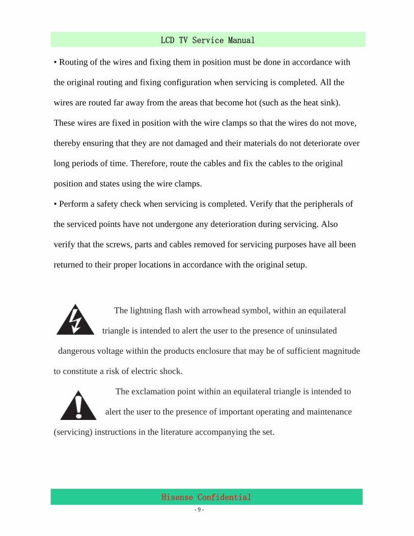
The lightning flash with arrowhead symbol, within an equilateral
triangle is intended to alert the user to the presence of uninsulated
dangerous voltage within the products enclosure that may be of sufficient magnitude
to constitute a risk of electric shock.
The exclamation point within an equilateral triangle is intended to
alert the user to the presence of important operating and maintenance
(servicing) instructions in the literature accompanying the set.
- 10 -
LCD TV Service Manual
Hisense Confidential
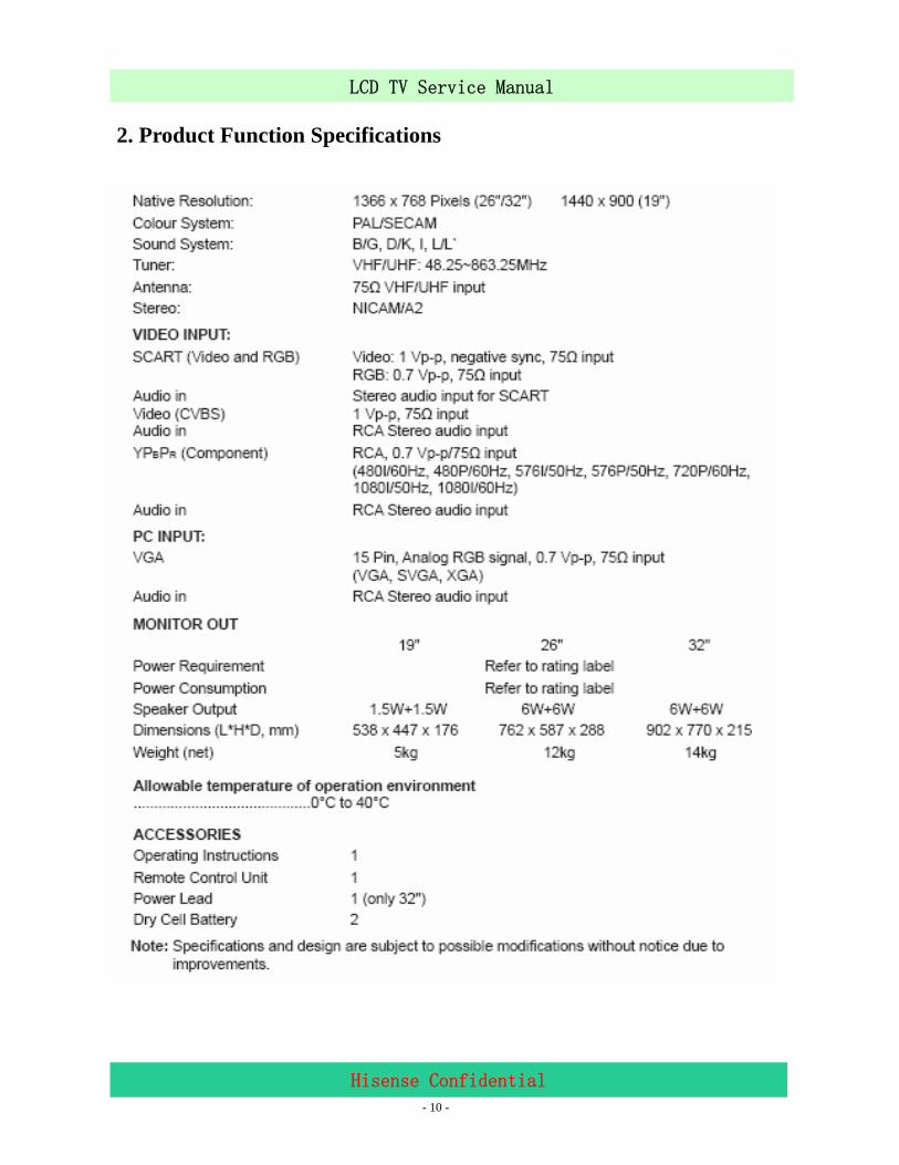
2. Product Function Specifications
- 11 -
LCD TV Service Manual
Hisense Confidential
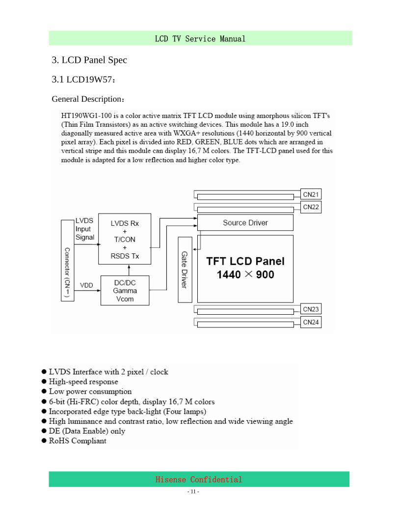
3. LCD Panel Spec
3.1 LCD19W57:
General Description:
- 12 -
LCD TV Service Manual
Hisense Confidential
3.2 LCD26W57:
General Description:
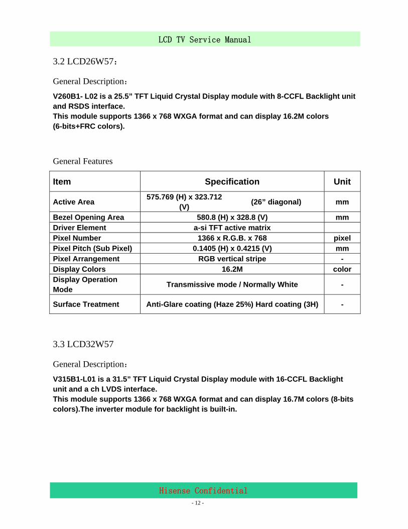
V260B1- L02 is a 25.5” TFT Liquid Crystal Display module with 8-CCFL Backlight unit and RSDS interface. This module supports 1366 x 768 WXGA format and can display 16.2M colors (6-bits+FRC colors).
General Features
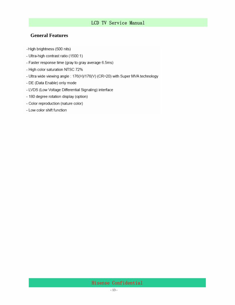
Item Specification Unit
Active Area 575.769 (H) x 323.712 (V) (26” diagonal) mm
Bezel Opening Area 580.8 (H) x 328.8 (V) mm Driver Element a-si TFT active matrix Pixel Number 1366 x R.G.B. x 768 pixel Pixel Pitch (Sub Pixel) 0.1405 (H) x 0.4215 (V) mm Pixel Arrangement RGB vertical stripe - Display Colors 16.2M color Display Operation Mode Transmissive mode / Normally White -
Surface Treatment Anti-Glare coating (Haze 25%) Hard coating (3H) -
3.3 LCD32W57
General Description:
V315B1-L01 is a 31.5” TFT Liquid Crystal Display module with 16-CCFL Backlight unit and a ch LVDS interface. This module supports 1366 x 768 WXGA format and can display 16.7M colors (8-bits colors).The inverter module for backlight is built-in.
- 13 -
LCD TV Service Manual
Hisense Confidential
General Features
- 14 -
LCD TV Service Manual
Hisense Confidential
4. Chassis Layout and Overall Wiring Diagrams
4.1 Chassis Layout
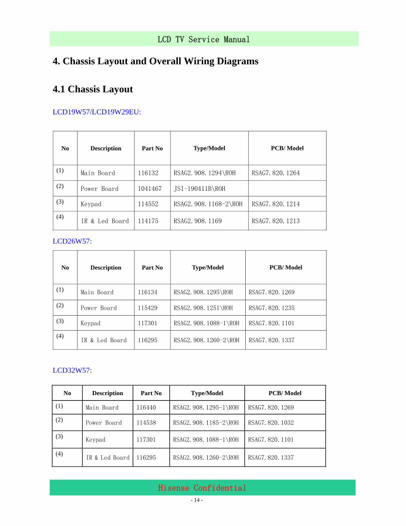
LCD19W57/LCD19W29EU:
LCD26W57:
LCD32W57:
No Description Part No Type/Model PCB/ Model
(1) Main Board 116440 RSAG2.908.1295-1\ROH RSAG7.820.1269
(2) Power Board 114538 RSAG2.908.1185-2\ROH RSAG7.820.1032
(3) Keypad 117301 RSAG2.908.1088-1\ROH RSAG7.820.1101
(4) IR & Led Board 116295 RSAG2.908.1260-2\ROH RSAG7.820.1337
No Description Part No Type/Model PCB/ Model
(1) Main Board 116132 RSAG2.908.1294\ROH RSAG7.820.1264
(2) Power Board 1041467 JSI-190411B\ROH
(3) Keypad 114552 RSAG2.908.1168-2\ROH RSAG7.820.1214
(4) IR & Led Board 114175 RSAG2.908.1169 RSAG7.820.1213
No Description Part No Type/Model PCB/ Model
(1) Main Board 116134 RSAG2.908.1295\ROH RSAG7.820.1269
(2) Power Board 115429 RSAG2.908.1251\ROH RSAG7.820.1235
(3) Keypad 117301 RSAG2.908.1088-1\ROH RSAG7.820.1101
(4) IR & Led Board 116295 RSAG2.908.1260-2\ROH RSAG7.820.1337
- 15 -
LCD TV Service Manual
Hisense Confidential
4.4 Wires and Cables Overall Wiring Diagrams
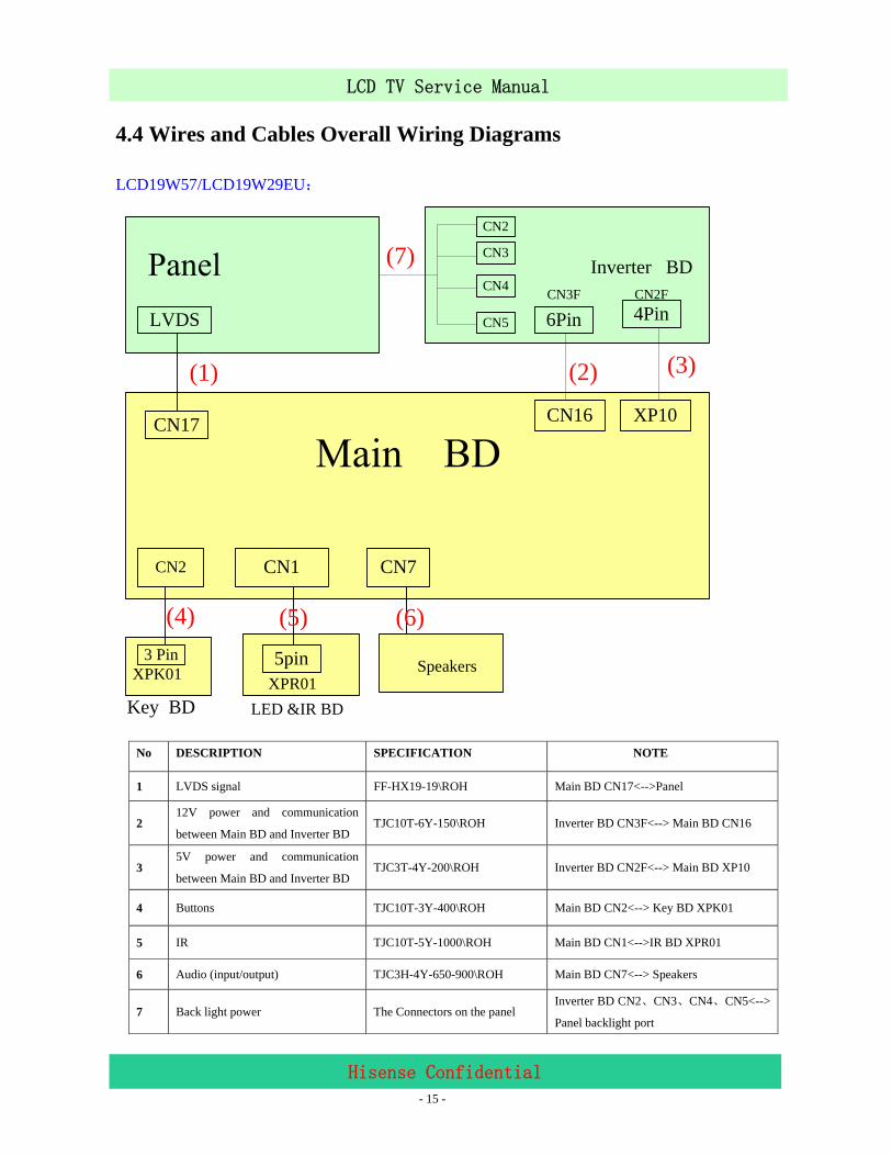
LCD19W57/LCD19W29EU:
CN2
CN3
LVDS
CN17
6PinCN3F
3 PinXPK01
Key BD
CN2
5pinXPR01
LED &IR BD
Speakers
CN1 CN7
Inverter BD
CN16
(1) (2)
(4) (5) (6)
(3)
CN4
CN5 4PinCN2F
XP10
(7)
No DESCRIPTION SPECIFICATION NOTE
1 LVDS signal FF-HX19-19\ROH Main BD CN17<-->Panel
2 12V power and communication
between Main BD and Inverter BD TJC10T-6Y-150\ROH Inverter BD CN3F<--> Main BD CN16
3 5V power and communication
between Main BD and Inverter BD TJC3T-4Y-200\ROH Inverter BD CN2F<--> Main BD XP10
4 Buttons TJC10T-3Y-400\ROH Main BD CN2<--> Key BD XPK01
5 IR TJC10T-5Y-1000\ROH Main BD CN1<-->IR BD XPR01
6 Audio (input/output) TJC3H-4Y-650-900\ROH Main BD CN7<--> Speakers
7 Back light power The Connectors on the panel Inverter BD CN2、CN3、CN4、CN5<-->
Panel backlight port
- 16 -
LCD TV Service Manual
Hisense Confidential
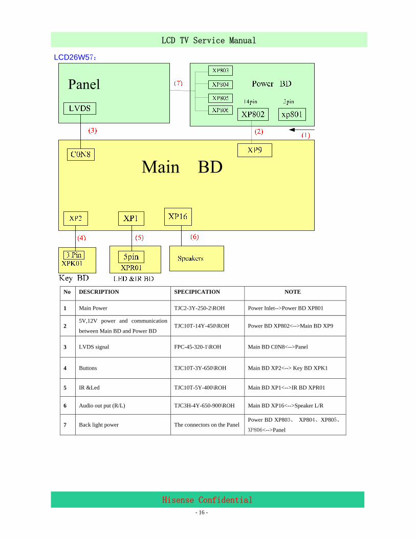
LCD26W57:
No DESCRIPTION SPECIPICATION NOTE
1 Main Power TJC2-3Y-250-2\ROH Power Inlet-->Power BD XP801
2 5V,12V power and communication
between Main BD and Power BD TJC10T-14Y-450\ROH Power BD XP802<-->Main BD XP9
3 LVDS signal FPC-45-320-1\ROH Main BD C0N8<-->Panel
4 Buttons TJC10T-3Y-650\ROH Main BD XP2<--> Key BD XPK1
5 IR &Led TJC10T-5Y-400\ROH Main BD XP1<-->IR BD XPR01
6 Audio out put (R/L) TJC3H-4Y-650-900\ROH Main BD XP16<-->Speaker L/R
7 Back light power The connectors on the PanelPower BD XP803、 XP804、XP805、
XP806<-->Panel
- 17 -
LCD TV Service Manual
Hisense Confidential
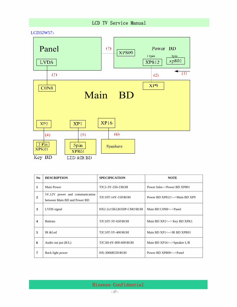
LCD32W57:
No DESCRIPTION SPECIPICATION NOTE
1 Main Power TJC2-3Y-250-2\ROH Power Inlet-->Power BD XP801
2 5V,12V power and communication
between Main BD and Power BD TJC10T-14Y-150\ROH Power BD XP812<-->Main BD XP9
3 LVDS signal HX2-2x15KLB350P-CMO\ROH Main BD C0N8<-->Panel
4 Buttons TJC10T-3Y-650\ROH Main BD XP2<--> Key BD XPK1
5 IR &Led TJC10T-5Y-400\ROH Main BD XP1<-->IR BD XPR01
6 Audio out put (R/L) TJC3H-4Y-800-600\ROH Main BD XP16<-->Speaker L/R
7 Back light power HX-3006B550\ROH Power BD XP809<-->Panel
- 18 -
LCD TV Service Manual
Hisense Confidential
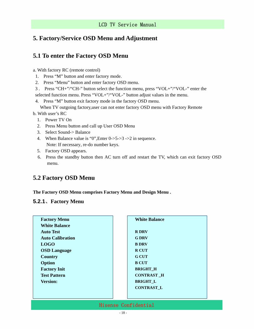
5. Factory/Service OSD Menu and Adjustment
5.1 To enter the Factory OSD Menu
a. With factory RC (remote control) 1. Press “M” button and enter factory mode. 2. Press “Menu” button and enter factory OSD menu. 3 . Press “CH+”/“CH-” button select the function menu, press “VOL+”/“VOL-” enter the selected function menu. Press “VOL+”/“VOL-” button adjust values in the menu. 4. Press “M” button exit factory mode in the factory OSD menu.
When TV outgoing factory,user can not enter factory OSD menu with Factory Remote b. With user’s RC
1. Power TV On 2. Press Menu button and call up User OSD Menu 3. Select Sound-> Balance 4. When Balance value is “0”,Enter 0->5->3 ->2 in sequence.
Note: If necessary, re-do number keys. 5. Factory OSD appears. 6. Press the standby button then AC turn off and restart the TV, which can exit factory OSD
menu.
5.2 Factory OSD Menu
The Factory OSD Menu comprises Factory Menu and Design Menu .
5.2.1、Factory Menu
White Balance
R DRV G DRV B DRV R CUT G CUT B CUT BRIGHT_H CONTRAST _H BRIGHT_L CONTRAST_L
Factory Menu White Balance Auto Test Auto Calibration LOGO OSD Language Country Option Factory Init Test Pattern Version:
- 19 -
LCD TV Service Manual
Hisense Confidential
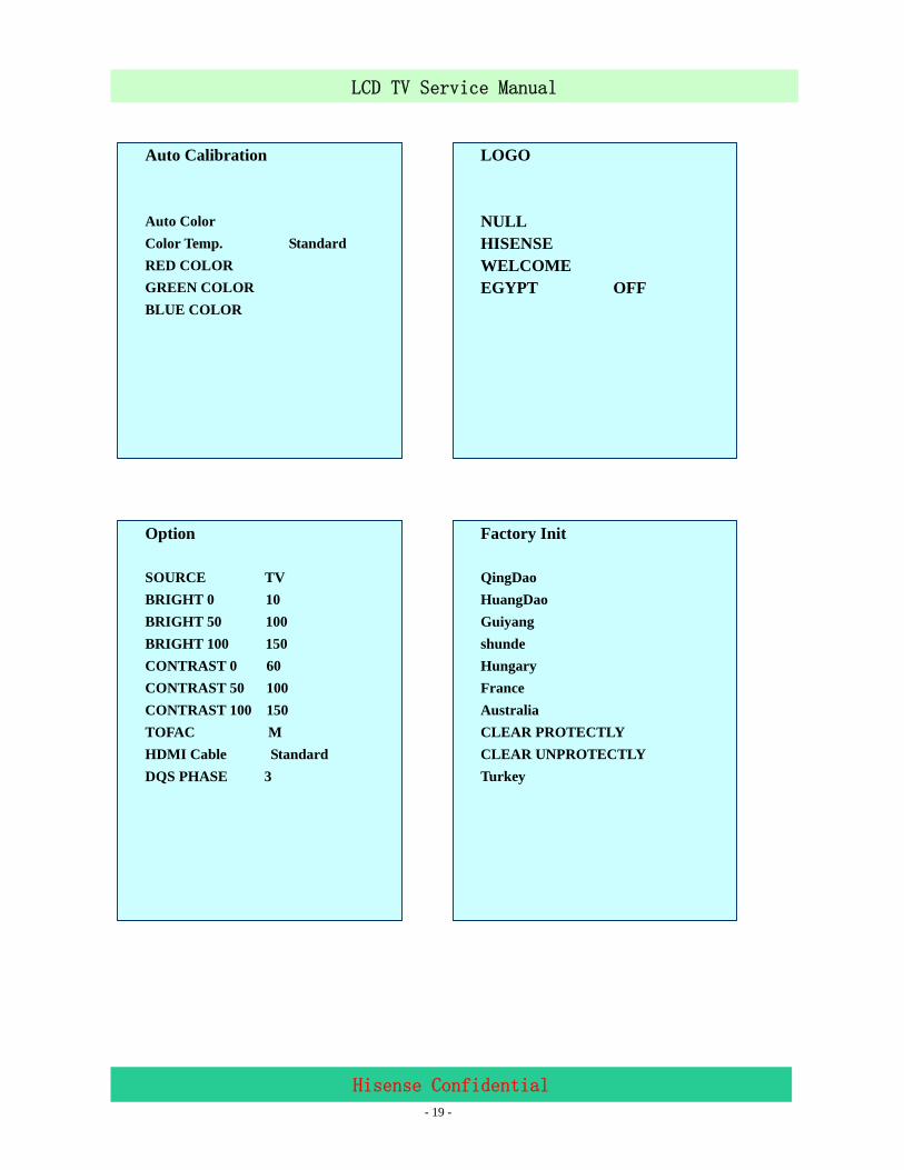
Factory Init
QingDao HuangDao Guiyang shunde Hungary France Australia CLEAR PROTECTLY CLEAR UNPROTECTLY Turkey
Option SOURCE TV BRIGHT 0 10 BRIGHT 50 100 BRIGHT 100 150 CONTRAST 0 60 CONTRAST 50 100 CONTRAST 100 150 TOFAC M HDMI Cable Standard DQS PHASE 3
LOGO
NULL HISENSE WELCOME EGYPT OFF
Auto Calibration
Auto Color Color Temp. Standard RED COLOR GREEN COLOR BLUE COLOR
- 20 -
LCD TV Service Manual
Hisense Confidential
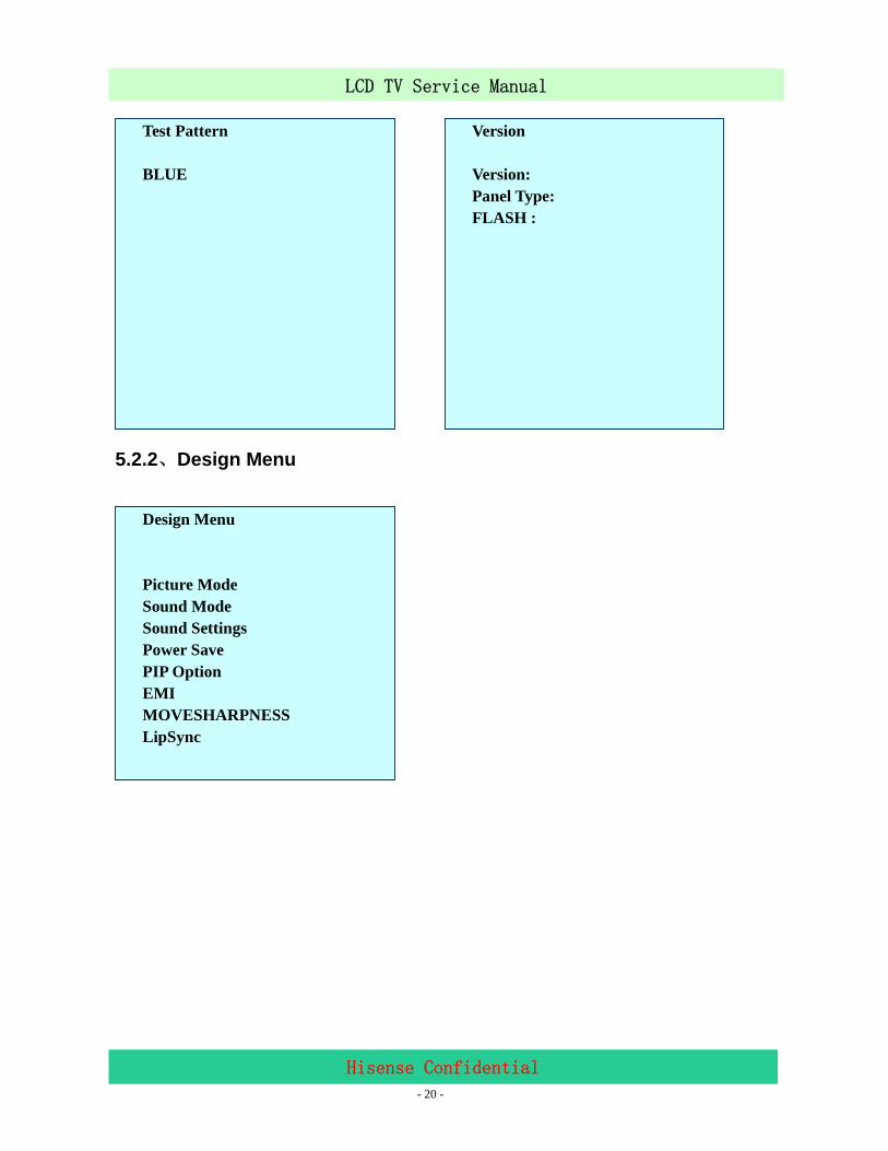
5.2.2、Design Menu
Design Menu Picture Mode Sound Mode Sound Settings Power Save PIP Option EMI MOVESHARPNESS LipSync
Version
Version: Panel Type: FLASH :
Test Pattern BLUE
- 21 -
LCD TV Service Manual
Hisense Confidential
Note:
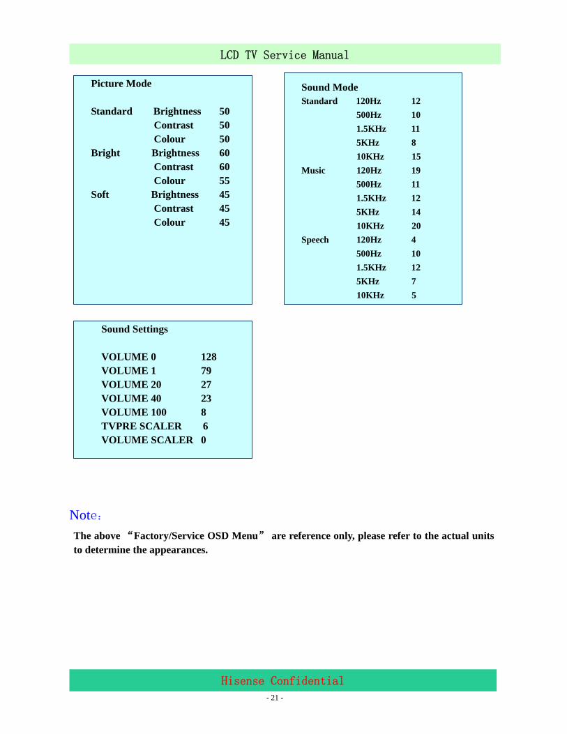
The above “Factory/Service OSD Menu” are reference only, please refer to the actual units to determine the appearances.
Sound Settings
VOLUME 0 128 VOLUME 1 79 VOLUME 20 27 VOLUME 40 23 VOLUME 100 8 TVPRE SCALER 6 VOLUME SCALER 0
Sound Mode Standard 120Hz 12 500Hz 10 1.5KHz 11 5KHz 8 10KHz 15 Music 120Hz 19 500Hz 11 1.5KHz 12 5KHz 14 10KHz 20 Speech 120Hz 4 500Hz 10 1.5KHz 12 5KHz 7 10KHz 5
Picture Mode Standard Brightness 50
Contrast 50 Colour 50
Bright Brightness 60 Contrast 60 Colour 55
Soft Brightness 45 Contrast 45 Colour 45
- 22 -
LCD TV Service Manual
Hisense Confidential
6. Software Upgrading
The software is upgraded by a burning tool- ISP_TOOL4.0.9, which can burn the program file “*.bin ”to the main board of the unit
6.1 Get ready for upgrading
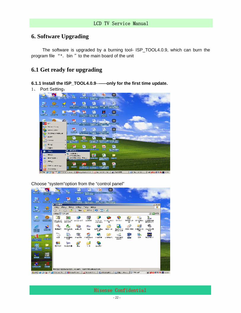
6.1.1 Install the ISP_TOOL4.0.9-------only for the first time update. 1、 Port Setting:
Choose “system”option from the “control panel”
- 23 -
LCD TV Service Manual
Hisense Confidential
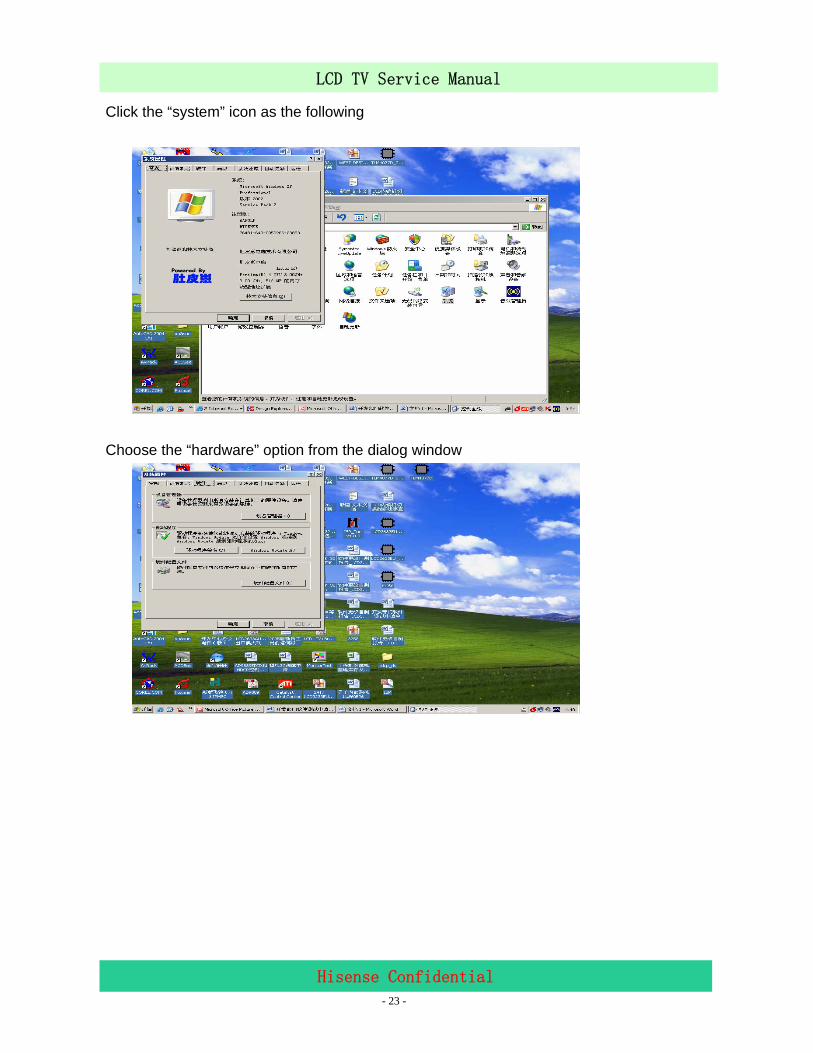
Click the “system” icon as the following
Choose the “hardware” option from the dialog window
- 24 -
LCD TV Service Manual
Hisense Confidential
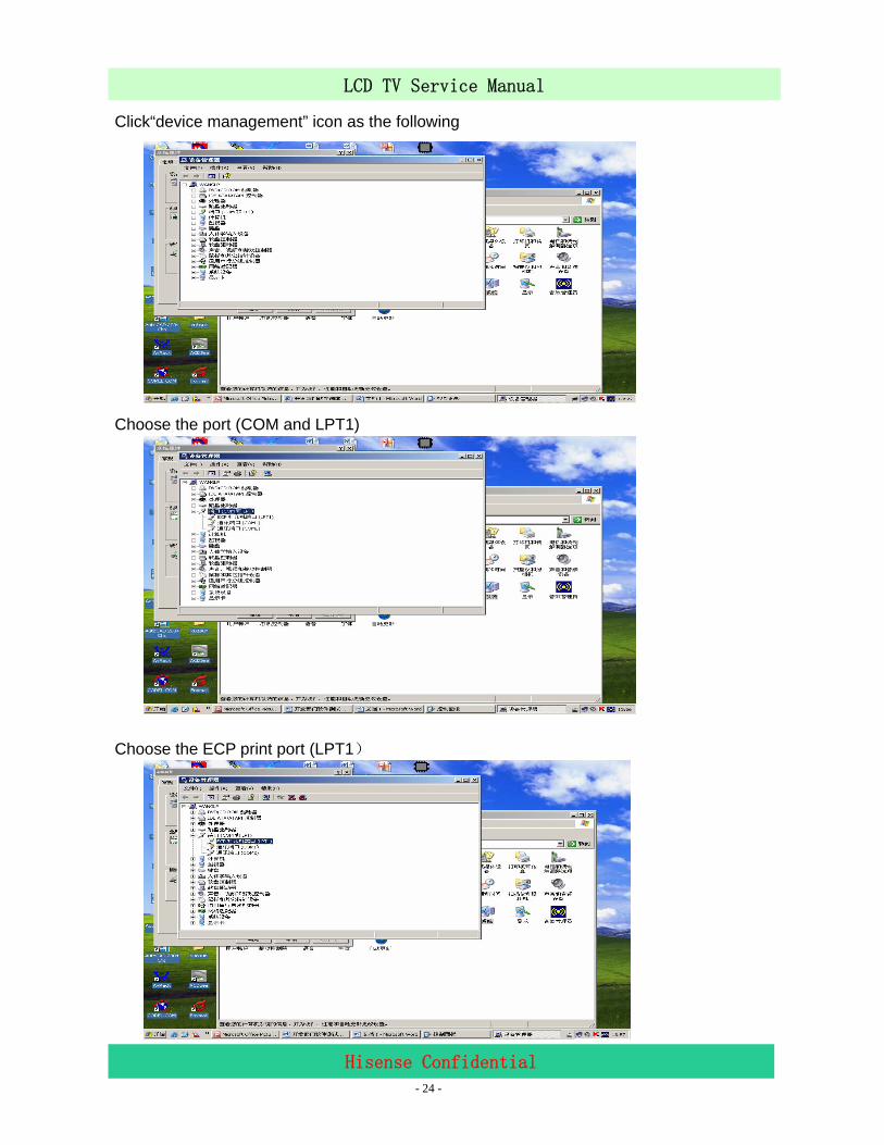
Click“device management” icon as the following
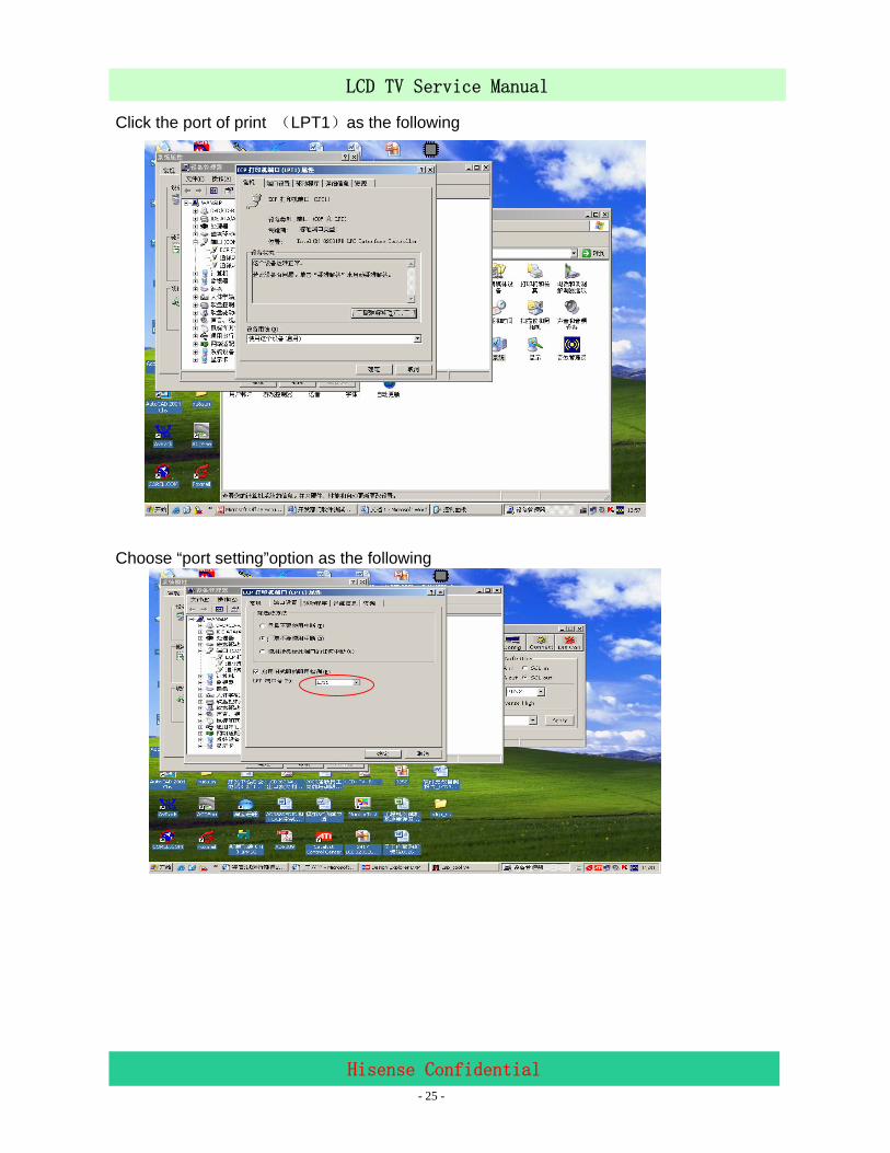
Choose the port (COM and LPT1)
Choose the ECP print port (LPT1)
- 25 -
LCD TV Service Manual
Hisense Confidential
Click the port of print (LPT1)as the following
Choose “port setting”option as the following
- 26 -
LCD TV Service Manual
Hisense Confidential
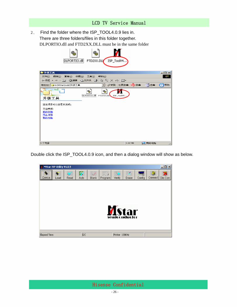
2、 Find the folder where the ISP_TOOL4.0.9 lies in. There are three folders/files in this folder together. DLPORTIO.dll and FTD2XX.DLL must be in the same folder
Double click the ISP_TOOL4.0.9 icon, and then a dialog window will show as below.
- 27 -
LCD TV Service Manual
Hisense Confidential
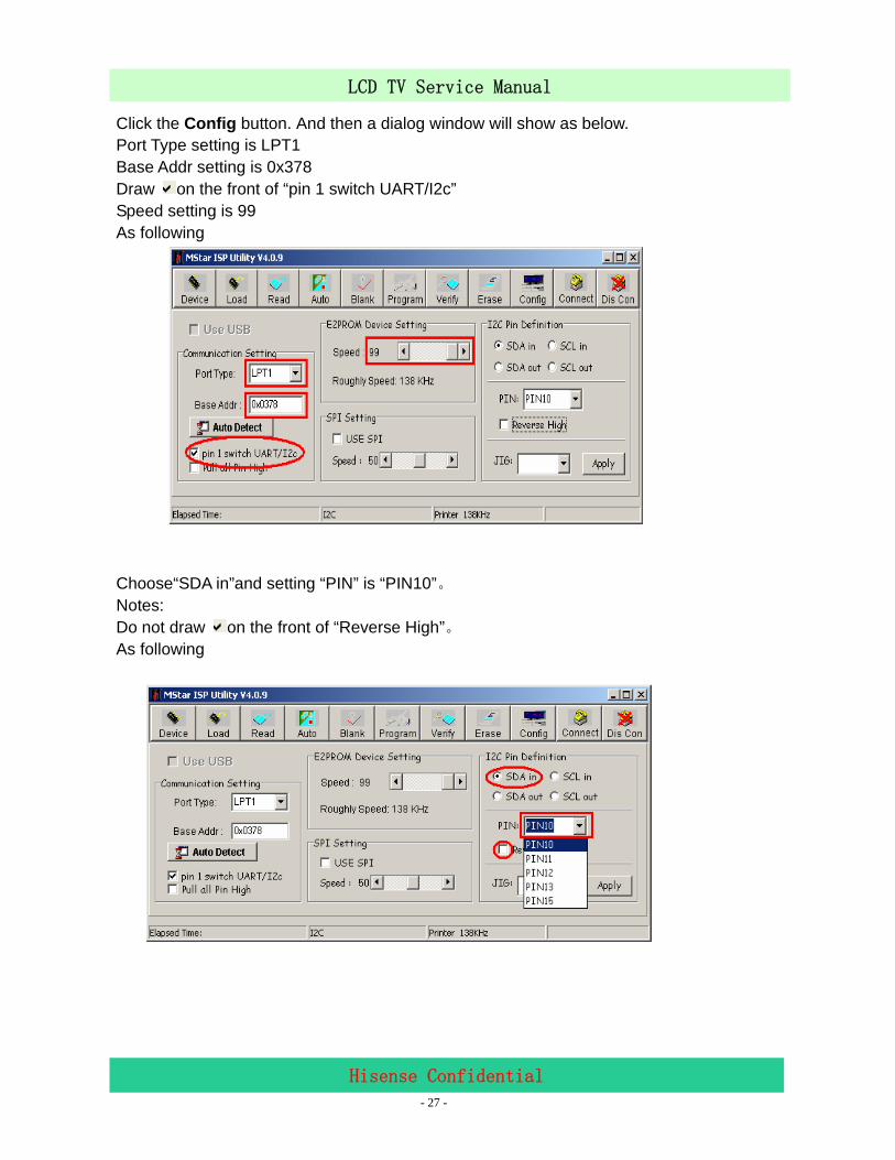
Click the Config button. And then a dialog window will show as below. Port Type setting is LPT1 Base Addr setting is 0x378 Draw on the front of “pin 1 switch UART/I2c” Speed setting is 99 As following
Choose“SDA in”and setting “PIN” is “PIN10”。 Notes: Do not draw on the front of “Reverse High”。 As following
- 28 -
LCD TV Service Manual
Hisense Confidential
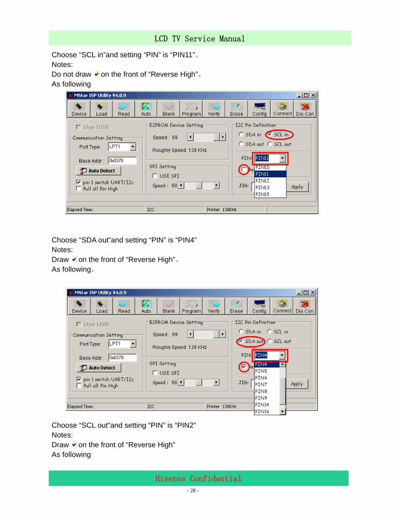
Choose “SCL in”and setting “PIN” is “PIN11”。 Notes: Do not draw on the front of “Reverse High”。 As following
Choose “SDA out”and setting “PIN” is “PIN4” Notes: Draw on the front of “Reverse High”。 As following。
Choose “SCL out”and setting “PIN” is “PIN2” Notes: Draw on the front of “Reverse High” As following
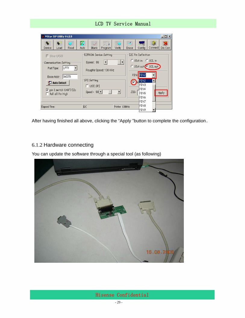
- 29 -
LCD TV Service Manual
Hisense Confidential
After having finished all above, clicking the “Apply ”button to complete the configuration。
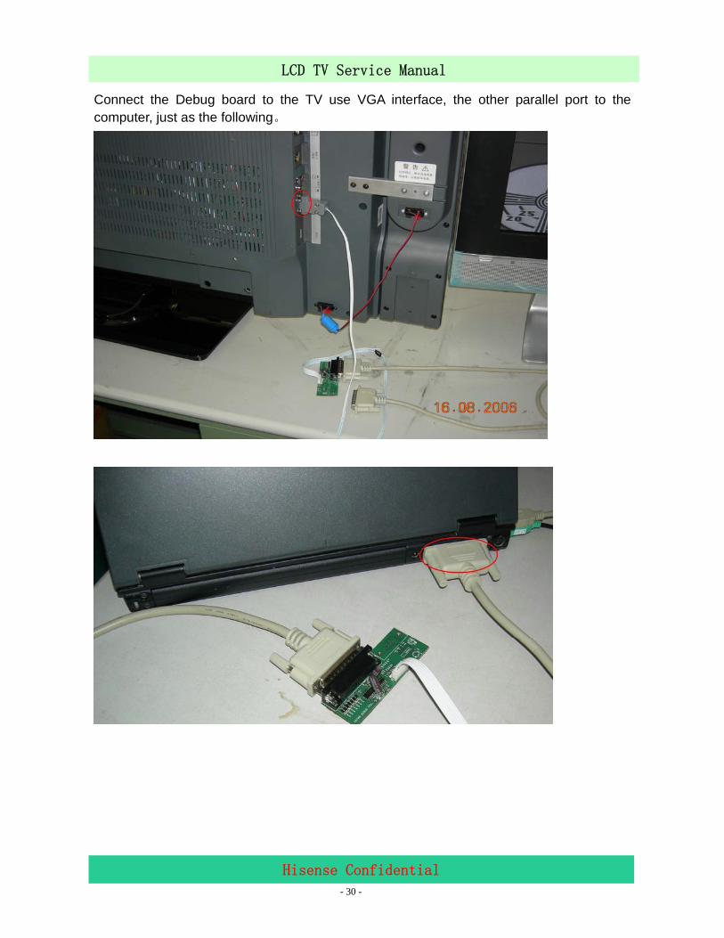
6.1.2 Hardware connecting You can update the software through a special tool (as following)
- 30 -
LCD TV Service Manual
Hisense Confidential
Connect the Debug board to the TV use VGA interface, the other parallel port to the computer, just as the following。
- 31 -
LCD TV Service Manual
Hisense Confidential
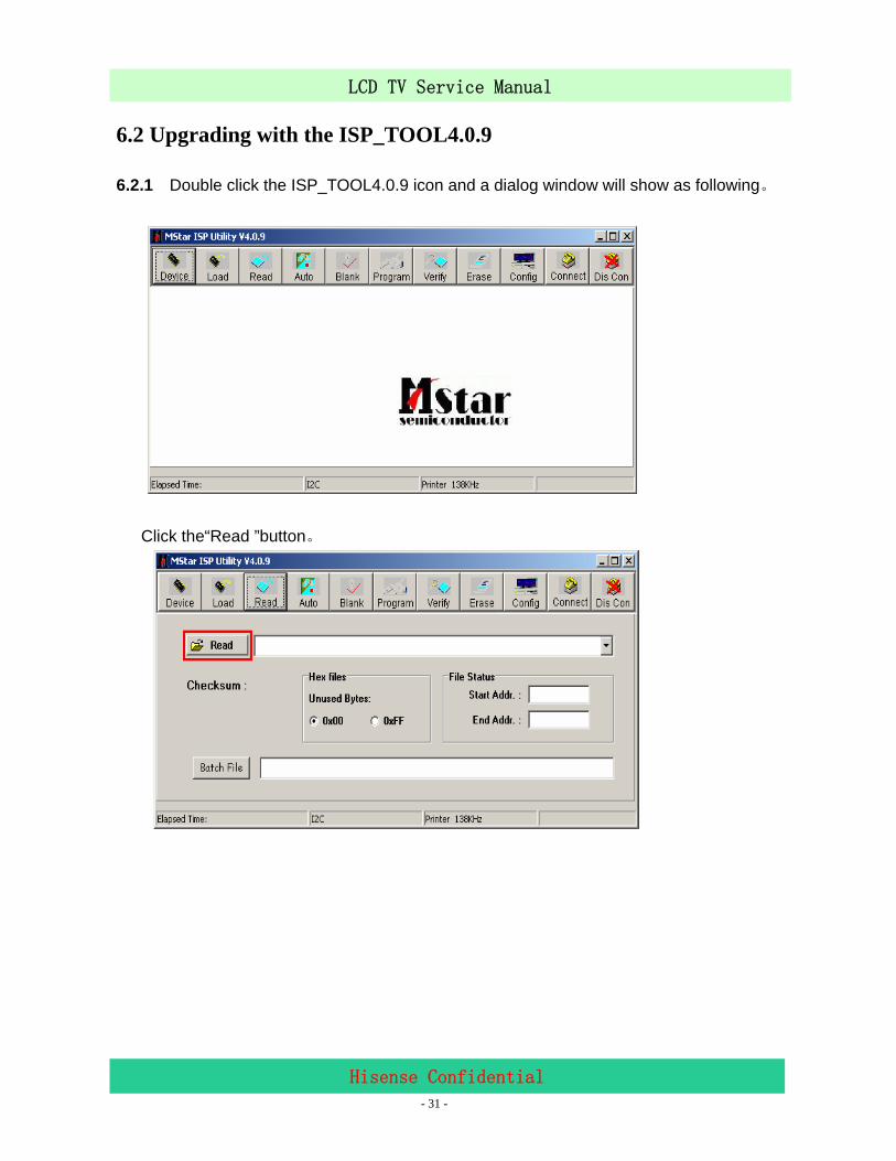
6.2 Upgrading with the ISP_TOOL4.0.9
6.2.1 Double click the ISP_TOOL4.0.9 icon and a dialog window will show as following。
Click the“Read ”button。
- 32 -
LCD TV Service Manual
Hisense Confidential
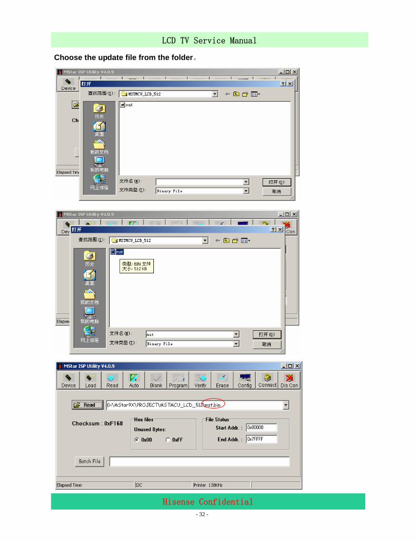
Choose the update file from the folder。
- 33 -
LCD TV Service Manual
Hisense Confidential
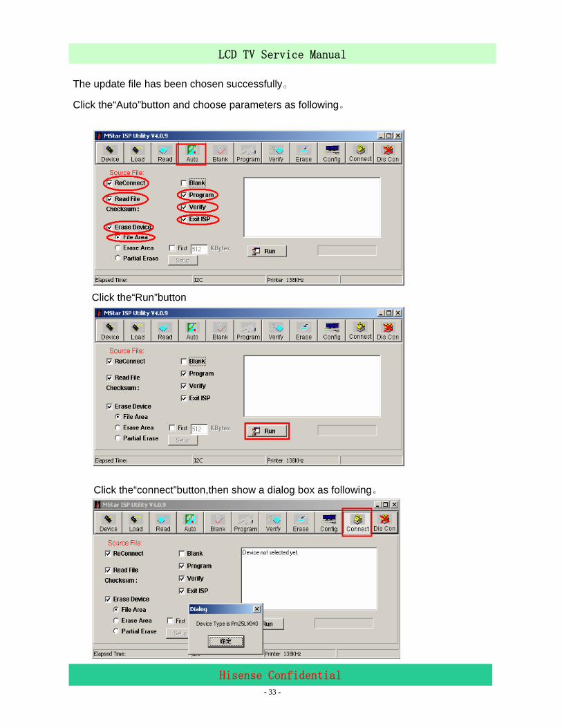
The update file has been chosen successfully。
Click the“Auto”button and choose parameters as following。
Click the“Run”button
Click the“connect”button,then show a dialog box as following。
- 34 -
LCD TV Service Manual
Hisense Confidential
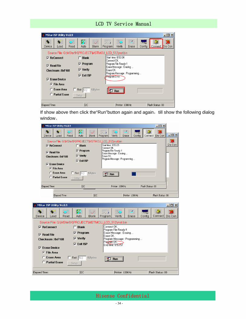
If show above then click the“Run”button again and again,till show the following dialog window。
- 35 -
LCD TV Service Manual
Hisense Confidential
The above appears on the screen-the word “program ok”shows in the information displaying window,indicating upgrading is over。
6.2.2 After the update is over. Must Confirm the software Version in the Version Menu. If the update is successful, enter Factory Init Menu and select “Clear Unprotectly” a. Press VOL+ button to clear the EEPROM data. b. When the “Clear Unprotectly ” button becomes white, turn off the power. c. Restart the TV.
- 36 -
LCD TV Service Manual
Hisense Confidential
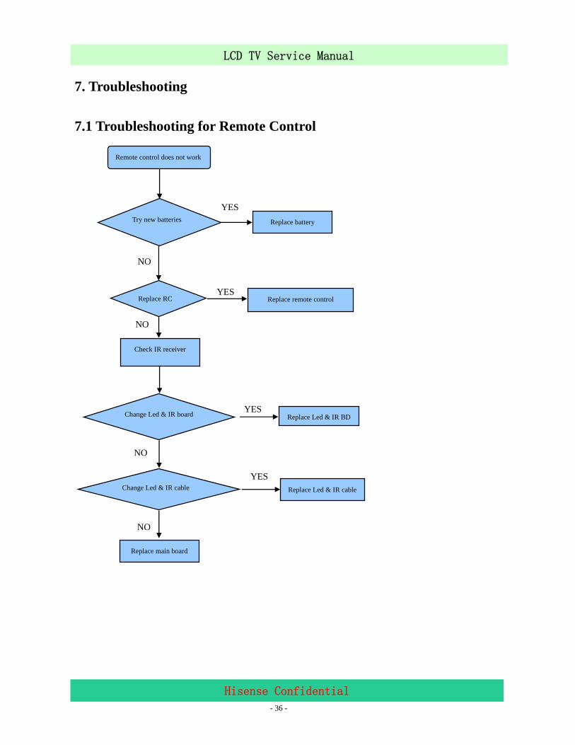
7. Troubleshooting
7.1 Troubleshooting for Remote Control
Remote control does not work
Try new batteries
Replace RC
Check IR receiver
Change Led & IR board
Change Led & IR cable
Replace main board
Replace battery
Replace remote control
Replace Led & IR BD
Replace Led & IR cable
YES
YES
NO
YES
NO
YES
NO
NO
- 37 -
LCD TV Service Manual
Hisense Confidential
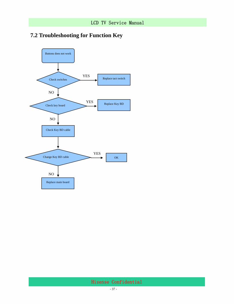
7.2 Troubleshooting for Function Key
Buttons does not work
Check switches
Check key board
Check Key BD cable
Change Key BD cable
Replace main board
Replace tact switch
Replace Key BD
OK
YES
YES
NO
YES
NO
NO
- 38 -
LCD TV Service Manual
Hisense Confidential
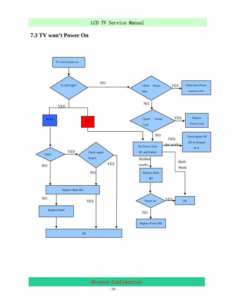
7.3 TV won’t Power On
Make Sure Power
source is live
Replace
Power Cord
Check/replace IR
BD or Keypad
PCA
TV won’t power on
Is LED light? NO
YES
Check Power
Inlet
YES
NO
Check Power
Cord
Only one works
Replace Main
BD
Try Power on by
RC and Button
Neither works
Both Work
Power on OK YES
NO
Replace Power BD
YES
NO
RED BLUE
OSD?
NO
Replace Main BD
NO
YES Check signal
Source
YES
NO
YES
Replace Panel
OK
- 39 -
LCD TV Service Manual
Hisense Confidential
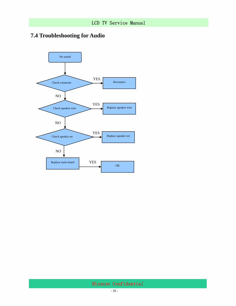
7.4 Troubleshooting for Audio
No sound
Check connecter
Check speaker wire
Replace main board
Reconnect
Replace speaker wire
YES
YES
NO
NO
Check speaker set Replace speaker set YES
NO
OK YES
- 40 -
LCD TV Service Manual
Hisense Confidential
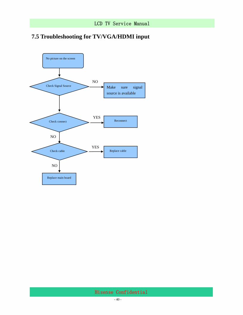
7.5 Troubleshooting for TV/VGA/HDMI input
No picture on the screen
Check Signal Source
Check connect
Check cable
Replace main board
Make sure signal source is available
Reconnect
Replace cable
NO
YES
YES
NO
NO
- 41 -
LCD TV Service Manual
Hisense Confidential
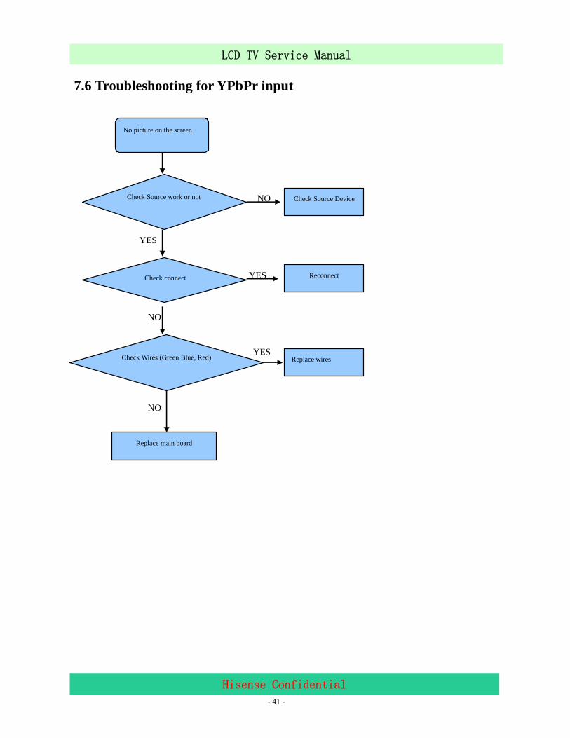
7.6 Troubleshooting for YPbPr input
No picture on the screen
Check Source work or not
Check connect
Check Wires (Green Blue, Red)
Replace main board
Check Source Device
Reconnect
Replace wires
NO
YES
YES
NO
YES
NO
- 42 -
LCD TV Service Manual
Hisense Confidential
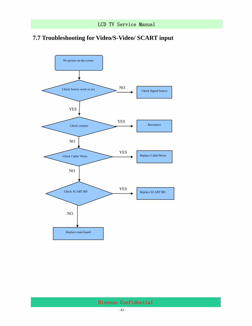
7.7 Troubleshooting for Video/S-Video/ SCART input
Replace SCART BD
Replace main board
NO
YES
No picture on the screen
Check Source work or not
Check connect
Check Cable/ Wires
Check Signal Source
Reconnect
Replace Cable/Wires
NO
YES
YES
NO
YES
NO
Check SCART BD
- 43 -
LCD TV Service Manual
Hisense Confidential
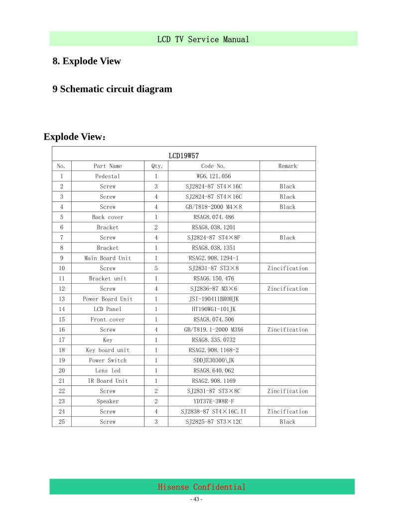
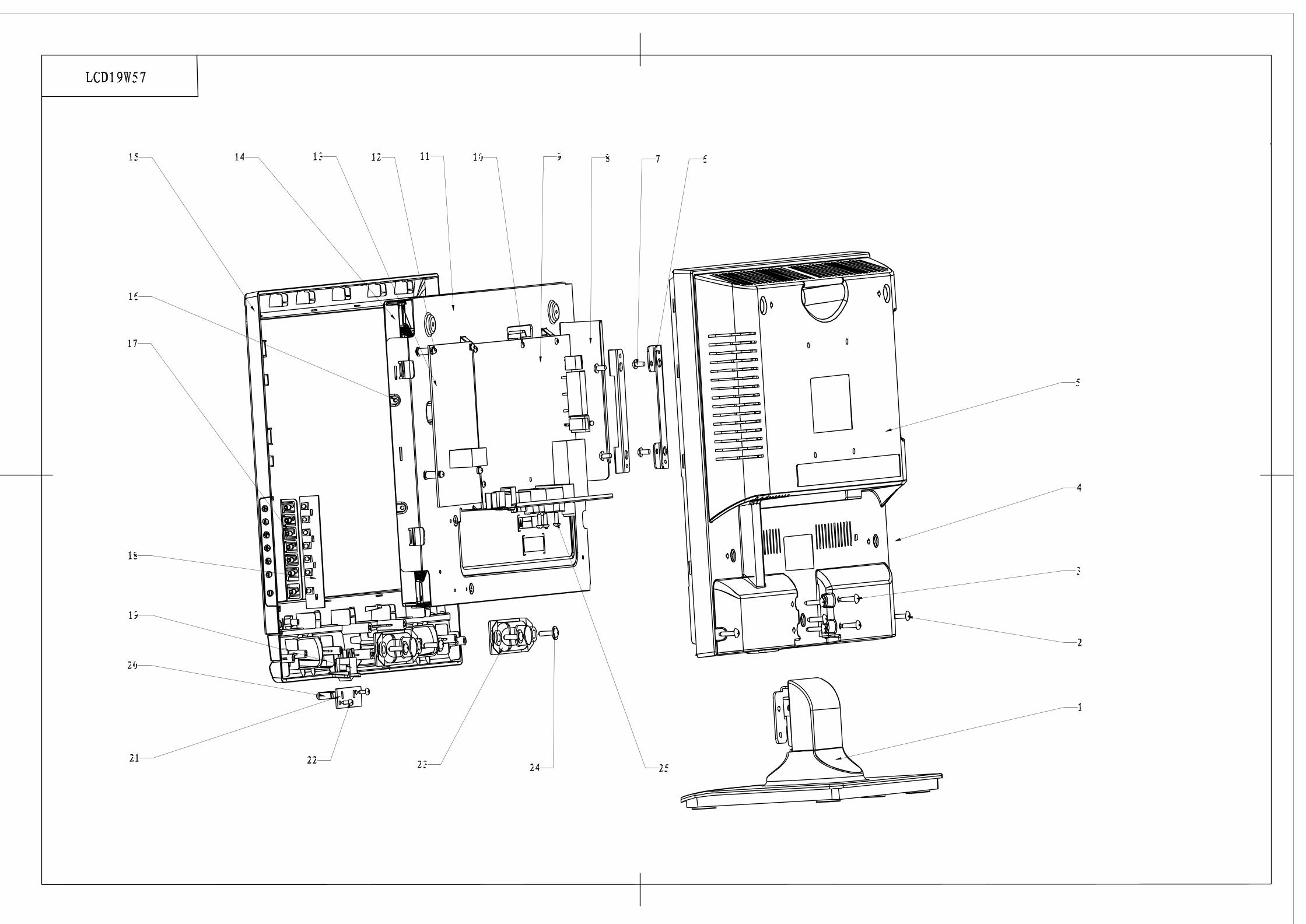
8. Explode View
9 Schematic circuit diagram
Explode View:
LCD19W57
No. Part Name Qty. Code No. Remark
1 Pedestal 1 WG6.121.056
2 Screw 3 SJ2824-87 ST4×16C Black
3 Screw 4 SJ2824-87 ST4×16C Black
4 Screw 4 GB/T818-2000 M4×8 Black
5 Back cover 1 RSAG8.074.486
6 Bracket 2 RSAG8.038.1201
7 Screw 4 SJ2824-87 ST4×8F Black
8 Bracket 1 RSAG8.038.1351
9 Main Board Unit 1 RSAG2.908.1294-1
10 Screw 5 SJ2831-87 ST3×8 Zincification
11 Bracket unit 1 RSAG6.150.476
12 Screw 4 SJ2836-87 M3×6 Zincification
13 Power Board Unit 1 JSI-190411BROHJK
14 LCD Panel 1 HT190WG1-101JK
15 Front cover 1 RSAG8.074.506
16 Screw 4 GB/T819.1-2000 M3X6 Zincification
17 Key 1 RSAG8.335.0732
18 Key board unit 1 RSAG2.908.1168-2
19 Power Switch 1 SDDJE30300\JK
20 Lens led 1 RSAG8.640.062
21 IR Board Unit 1 RSAG2.908.1169
22 Screw 2 SJ2831-87 ST3×8C Zincification
23 Speaker 2 YDT37E-3W8R-F
24 Screw 4 SJ2838-87 ST4×16C.II Zincification
25 Screw 3 SJ2825-87 ST3×12C Black
5
5
4
4
3
3
2
2
1
1
D D
C C
B B
A A
BL-ADJ
ADJ-PWM3
STANDBY
POWER-ON/OFFPOWER-ON/OFF
BL-ON/OFF
ON-PBACK
SCL_EXT
KEY1-inPOWER-ON/OFFRTC_INT
MCU_CNT
LED-MCU1
IR-in
IPWM|GND
SDA_EXT
BL-ADJ
BL-ON/OFFIPWM|GND
STANDBY
+12V_in
5Vstb
5Vstb
5Vstb
5Vstb
5Vstb+5V_mst
+3.3Vstb
+5V_in +5V_all
+12V_in +12V_all
+5V_all
+5V_in+5V_in
+12V_in+12V_in
5Vstb5Vstb
ADJ-PWM3
ON-PBACK
POWER-ON/OFF
IR-in MCU_CNT
LED-MCU1 POWER-ON/OFFKEY1-in
SCL_EXT
SDA_EXT
Title
Size Document Number Rev
Date: Sheet of
MST9E19A 2.0
<Title>
A3
1 19Tuesday, January 22, 2008
Title
Size Document Number Rev
Date: Sheet of
MST9E19A 2.0
<Title>
A3
1 19Tuesday, January 22, 2008
Title
Size Document Number Rev
Date: Sheet of
MST9E19A 2.0
<Title>
A3
1 19Tuesday, January 22, 2008
TO Inverter Board
同1319 E版修改
R20 NC/100R20 NC/100
+
CA4 NC/10uF/16V
+
CA4 NC/10uF/16V
R1310KR1310K
C102.2uFC102.2uF
V43904V43904
1
23
R14.7KR14.7K
N4
NC/PT7C4363
N4
NC/PT7C4363
X11X22SCL6SDA5 GND 4BACKUP 3SCW/INT 7VCC 8
Z1
NC/32.768KHZ
Z1
NC/32.768KHZ12 + CA5
NC/10uF/16V
+ CA5
NC/10uF/16V
R19 NC/100R19 NC/100
R303NCR303NC
R3100R3100
R15 NCR15 NC
V13904V13904
1
23
C20.1uFC20.1uF
R44.7KR44.7K
V63904V63904
1
23
R2NCR2NC
R181KR181K
+CA1470uF/16V
+CA1470uF/16V
R164.7KR16
4.7K
R121KR121K
C9
NC/0.1uF
C9
NC/0.1uF
R22
NC/100
R22
NC/100
R214.7KR214.7K
BT1NC/BATTERYBT1NC/BATTERY
21
N3
NC/PIC12F629
N3
NC/PIC12F629
VCC1GP52GP43GP34 GP2 5GP1 6GP0 7GND 8C7 NC/0.1uFC7 NC/0.1uF
4 3 2 1
5 6 7 8
RP1
NC/RP4.7KX4
4 3 2 1
5 6 7 8
RP1
NC/RP4.7KX4
W2W2
XP9XP9
1234567891011121314
R304
4.7K
R304
4.7K
5
5
4
4
3
3
2
2
1
1
D D
C C
B B
A A
DMP_DTV-LSC/RC_GREEN SC/RC_BLUE
SC/RC_RED
ON_USBIR-in
DMP_DTV-R
IO1
ON_USB
SC1_VOUT
VCC_USB5V
5Vstb
VCC_USB5V
+12V_all
+12V_in
DMP_DTV-L
TXD2,4
SC/RC_BLUE 5SC/RC_RED5
SC1_VOUT6
SC/RC_GREEN5
RXD
DMP_DTV-R
ON_USB 1,2IO1
IR-in
ON_USB1,2
Title
Size Document Number Rev
Date: Sheet of
<Doc> <RevCod
<Title>
A3
1 1Saturday, December 15, 2007
Title
Size Document Number Rev
Date: Sheet of
<Doc> <RevCod
<Title>
A3
1 1Saturday, December 15, 2007
Title
Size Document Number Rev
Date: Sheet of
<Doc> <RevCod
<Title>
A3
1 1Saturday, December 15, 2007
528 amend
528 amendMAX:3A
MP1583
U11MP1583
MP1583
U11MP1583
IN2
GND4 SW3 COMP 6
SYN 8BS1EN 7
FB 5
GN
D9
R536 0R536 0
C389
1.5nF
C389
1.5nF
R451
33K
R451
33K
C396
16V 470uF
C396
16V 470uF
R40 4.7KR40 4.7K
R5260 R5260
D2
SMB5818
D2
SMB5818
C392
100P
C392
100PR520 0R520 0
Q63904Q63904
1
23
R352200KR352200K
R130 10KR130 10KQ7
3904
Q7
3904
1
23
C390
100P
C390
100P
R4454.7KR4454.7K
C391
100P
C391
100P
R51 4.7KR51 4.7K
C369
47uF
C369
47uF
R44710KR44710K
C397
100P
C397
100P
R440100KR440100K
C105
0.1uF
C105
0.1uF
XS11
40P-2X20
XS11
40P-2X20
16 Y_OUT
GND 2324 GND
GND38
GND 17
2 USB3_5V4 GND6 USB2_5V8 GND
10 USB1_5V12 GND
DM3 1DP3 3DM2 5DP2 7DM1 9DP1 11
13ML_OUT14 MR_OUTPB_OUT 15
18 PR_OUTCOM_PB 1920 COM_PR
COM_Y 2122 CVBS_IN
RXD 2526 TXD28 REMOTE
GPIO130 GPIO2 29POWER_USB 27
SCL132NC34 SDA1 31
ID 33VCC5V36 VCC5V 35
GND 37ML_IN 39MR_IN40
L77
4.7uH
L77
4.7uH
R72
100/NC
R72
100/NC
5
5
4
4
3
3
2
2
1
1
D D
C C
B B
A A
POWER-ON/OFF
EN
OUT
FB
EN
OUT
FB
+5V_mst+3.3Vstb
+3.3Vstb
+3.3VA AVDD_MemPLL
+3.3VA AVDD_AU
+3.3VA AVDD_SIF
+3.3VA AVDD_HDMI
+3.3Vstb VDDP VDDC
+3.3VA AVDDA
VDDC
5Vstb
VDD_MPLL
+3.3Vstb
+3.3VA
5Vstb
POWER-ON/OFF
Title
Size Document Number Rev
Date: Sheet of
<Doc> 2.0
<Title>
A3
Monday, February 04, 2008
Title
Size Document Number Rev
Date: Sheet of
<Doc> 2.0
<Title>
A3
Monday, February 04, 2008
Title
Size Document Number Rev
Date: Sheet of
<Doc> 2.0
<Title>
A3
Monday, February 04, 2008
Title
Size Document Number Rev
Date: Sheet of
深圳市高新区南区科技南十路国际技术创新研究院C座4楼
TEL:0755-26996895 FAX:0755-26996830
MST9E19A
power
A3
2 19Monday, February 04, 2008
Title
Size Document Number Rev
Date: Sheet of
深圳市高新区南区科技南十路国际技术创新研究院C座4楼
TEL:0755-26996895 FAX:0755-26996830
MST9E19A
power
A3
2 19Monday, February 04, 2008
Title
Size Document Number Rev
Date: Sheet of
深圳市高新区南区科技南十路国际技术创新研究院C座4楼
TEL:0755-26996895 FAX:0755-26996830
MST9E19A
power
A3
2 19Monday, February 04, 2008
Vcc3.3for MST9E19A analog
Vcc3.3for MST9E19A Digital
3.3V for AVDDPLL2 +3.3V for
VDD_MPLL
+3.3AVDD forAVDD_AU
+3.3AVDD for AVDD_SIF
pin6,pin12
+3.3AVDD forAVDD_HDMI
Vcc1.8 for MST9E19A
0.81*(1+Rup/Rdown)=1.8V---Rup=10K, Rdown=8.2K
pin36
+3.3AVDD forAVDDA
VDDC for MST9E19A Core
236
C32
NC/10nF
C32
NC/10nF
+CA10
106M
+CA10
106M
N7NC/MP2359N7NC/MP2359
EN4
FB 3
VCC5 OUT 6
BST 1
GND2
C310.1uFC310.1uF
C15NCC15NC
R41NC/1K
R41NC/1K
C340.1uFC340.1uF
C240.1uFC240.1uF
C280.1uFC280.1uF
C420.1uFC420.1uF
C390.1uFC390.1uF
C400.1uFC400.1uF
C202.2uFC202.2uF
D61 NC/IN4148D61 NC/IN4148
ADJ
OUT IN
N5AZ1084
ADJ
OUT IN
N5AZ1084
321
4
C120.1uFC120.1uF
C16NCC16NC
R25 10KR25 10K
D8B/240A
D8B/240A
C410.1uFC410.1uF
R263KR263K
R243.9KR243.9K
C430.1uFC430.1uF
C172.2uFC172.2uF
N6AP1520N6AP1520
OCSET3
FB 1
VCC4 OUT 6
OUT 5
EN
2V
ss7
Vss
8
C252.2uFC252.2uF
C360.1uFC360.1uF
C190.1uFC190.1uF
C47
0.1uF
C47
0.1uF
L8 BLM18PG181SN1L8 BLM18PG181SN1
+ CA647uF/16V
+ CA647uF/16V
V37
NC/AO3401
V37
NC/AO34013
1
2
L12BLM18PG181SN1L12BLM18PG181SN1
+
CA8106M
+
CA8106M
L14 BLM31PG121SN1L14 BLM31PG121SN1
C272.2uFC272.2uF
C350.1uFC350.1uF
L9 BLM18PG181SN1L9 BLM18PG181SN1
C45
0.1uF
C45
0.1uF
L13 BLM18PG181SN1L13 BLM18PG181SN1
C232.2uFC232.2uF
+ CA747uF/16V
+ CA747uF/16V
C300.1uFC300.1uF
+
CA9470uF
+
CA9470uF
+ CA1247uF/16V
+ CA1247uF/16V
L32BLM18PG181SN1L32BLM18PG181SN1
C130.1uFC130.1uF
C260.1uFC260.1uF
C370.1uFC370.1uF
L10BLM18PG181SN1L10BLM18PG181SN1
C48
0.1uF
C48
0.1uF
C210.1uFC210.1uF
C110.1uFC110.1uF
R233KR233K
C292.2uFC292.2uF
12
C380.1uFC380.1uF
C180.1uFC180.1uF
L11 BLM18PG181SN1L11 BLM18PG181SN1
L715uH
L715uH
12
C46
0.1uF
C46
0.1uF
C14
0.1uF
C14
0.1uF
C44
0.1uF
C44
0.1uF
C222.2uFC222.2uF
L6BLM31PG121SN1L6BLM31PG121SN1
C49
0.1uF
C49
0.1uF
5
5
4
4
3
3
2
2
1
1
D D
C C
B B
A A
WP
PWM2
SPI_CZ
AUOutL3
PWM2ADJ-PWM3
SPI_CK
PWM1/WP_FSH
I2C-SCLTXDRXD
PWM0
TXDRXD
DDC-RDX
HDMI_SCLHDMI_SDA
HDMI_SCL
G_TX1+
HDMI_SDA
BIN-
GIN-GIN+SOG
RIN+
BIN+
RIN-
VS_RGB
BIN-
GIN-
RIN-
R_TX2-
RIN+
HS_RGB
GIN+
SOG
BIN+
SCB+
SCR-SCG+
SCR+
SCB-
SCG-
R_TX2+
G_TX1-
B_TX0-B_TX0+
TXCLK+
PWM0
TXCLK-
SPI_DO
PWM1/WP_FSHKEY1KEY0
SCG-
SCR-SCR+
SCB-SCB+
SCG+
IR_SYNCSDA
PWM1/WP_FSH
AMP-Rout
AMP-Lout
SCL
SC_SOG
DDC-TXD
ADJ-PWM3
SC_SOG
TV-SIFP SIFPTV-SIFM SIFM
KEY1-inKEY0-in
AMP-R
AMP-L
I2C-SDAI2C-SCL
AUOut2-R
AUOut2-L
AUOutR2
AUOutL2
TXCLK+TXCLK-
B_TX0-B_TX0+
R_TX2+
G_TX1+G_TX1-
R_TX2-
HS_RGBVS_RGB
VCOM1TUNER_CVBS
SV_C0
VCOM0
SV_Y0VCOM2
SV_C0SV_Y0VCOM2CVBS3CVBS2CVBS1VCOM1
TUNER_CVBSVCOM0CVBSOut
S1-Cin
S1-Yin-
AV2/SC1-Vin+
S1-Yin
TV1-Vin+
CVBS3
TV1-Vin-
CVBS2CVBS1
AV1-Vin+
SIFMSIFP
AUOutL3AUOutR3
PC-RinPC-Lin
AUCOMAV1-RinAV1-Lin
AV2/SC1-RinAV2/SC1-Lin
AMP-RoutAMP-LoutAUOutR2AUOutL2
AUVRADNAUVRADPAUVREF
AUVRADN
AUVRADP
I2C-SDA
SPI_DI
SPI_DI
SPI_DO
SPI_CK
SPI_CZ
AUOutR3
KEY0
SYS_RST
AUVREF
SCLSDA
WP_EP
RXE1-/G1RXE1+/G0RXE2-/B7
RXE0-/G3RXE0+/G2
RXE2+/B6RXEC-/B5RXEC+/B4RXE3-/B3RXE3+/B2
SV_C1SV_Y1
SV_C1SV_Y1
LED_RED
LED-MCU1
LED_GREEN
IR-inIR-in_USB
KEY1
IR_SYNC
HD-VSW0
MCU_CNTHDMI_WP
ON-PBACK
SCL_EXTSDA_EXT
AMP-MUTEOverdrive
SCL
WP
PANEL-ON/OFF
LED_GREENLED_RED
HPDCTRL
KEY1-inKEY0-inKEY1-in
IR-in
LED-R
SDA
WP_EPWP_EP
POWER-ON/OFF
RXE3+/B2RXEC+/B4RXE2+/B6RXE1+/G0RXE0+/G2
BRI_OUT
RXE0-/G3
RXE3-/B3RXEC-/B5RXE2-/B7RXE1-/G1
BRI_OUT LVDS-SL/SCL
LVDS-SL/SCL
IO3IO2
IO1IO1IO1
IO4
SC_FSWSC_FS
SC_FSSC_FSW
AUOut3-R
AUOut3-L
LED-R
+5V_mst
VDDP
AVDD_HDMI
VDDP
+5V_mst
+3.3Vstb
VDDP
AVDD_MemPLL
VDDCVDD_MPLL
AVDD_AU
AVDD_SIF
AVDDA
AVDD_HDMIVDDP
+5V_mst
5Vstb
5Vstb
VDDP
+5V_mst
+5V_mst
5Vstb
VDDP
5Vstb
VCC-Panel
VCC-Panel
+3.3Vstb
VDDP
5Vstb
B_TX0+B_TX0-
R_TX2+
TXCLK+
R_TX2-
TXCLK-
HDMI_SCL
G_TX1+
HDMI_SDA
G_TX1-
TV-SIFPTV-SIFM
AMP-L
AMP-R
AUOut2-L
AUOut2-R
PC-RinPC-Lin
AV1-LinAV1-Rin
AV2/SC1-LinAV2/SC1-Rin
TXDRXD
HS_RGBVS_RGB
BIN+BIN-
SOG
GIN+GIN-
RIN+RIN-
SC_SOGSCR+SCR-SCG+SCG-SCB+SCB-
S1-CinS1-Yin
S1-Yin-
AV1-Vin+AV2/SC1-Vin+
TV1-Vin+TV1-Vin-
RXE0-/G3RXE0+/G2RXE1-/G1RXE1+/G0RXE2-/B7RXE2+/B6RXEC-/B5RXEC+/B4RXE3-/B3RXE3+/B2
KEY1-in
LED-MCU1
IR-in
HD-VSW0
ADJ-PWM3
SDA_EXTSCL_EXT
AMP-MUTE
ON-PBACKPOWER-ON/OFF
MCU_CNT
PANEL-ON/OFF
HPDCTRL
HDMI_WP
SPDIF_OUT
USB-PW
IO3IO2
IO1
IO4
SC2-LinSC2-Rin
CVBSOut
SC_FSWSC_FS
AUOut3-R
AUOut3-L
Title
Size Document Number Rev
Date: Sheet of
深圳市高新区南区科技南十路国际技术创新研究院C座4楼
TEL:0755-26996895 FAX:0755-26996830
MST9E19A 2.0
MST9E19A
A2
3 19Wednesday, January 23, 2008
Title
Size Document Number Rev
Date: Sheet of
深圳市高新区南区科技南十路国际技术创新研究院C座4楼
TEL:0755-26996895 FAX:0755-26996830
MST9E19A 2.0
MST9E19A
A2
3 19Wednesday, January 23, 2008
Title
Size Document Number Rev
Date: Sheet of
深圳市高新区南区科技南十路国际技术创新研究院C座4楼
TEL:0755-26996895 FAX:0755-26996830
MST9E19A 2.0
MST9E19A
A2
3 19Wednesday, January 23, 2008
I2C addressat A0.
Location Near IC Pin.
Mode Selection
Debug port
Location Near IC Pin.
WP:Mstar PULL DOWN
DVI
INPU
TVG
AIN
PUT
SCAR
TIN
PUT
Location Near IC Pin.
VIDE
OIN
PUT
HDCP I2C addressat A4.
GPIOF_SEL=01,VDO_PORT_SEL=00 for I2S input
AU_SWAP=11
Debug port
Location Near IC
LG NEW CHANGE PVR IO
R63
NC/4.7K
R63
NC/4.7K
V42
NC
V42
NC
1
23
R4322KR4322K
CA1510uF/16VCA1510uF/16V
R1954K7R1954K7
C67
100pF
C67
100pF
C73 10nFC73 10nF
R158NC/470
R158NC/470
D100
INPAQ_VPORT
D100
INPAQ_VPORT
12
R59 1KR59 1K
CA1610uF/16VCA1610uF/16V
CA1410uF/16VCA1410uF/16V
R891KR891K
R901KR901K
D9BAV99D9BAV99
3
2
1
4 3 2 1
5 6 7 8
RP14
RP4.7KX4
4 3 2 1
5 6 7 8
RP14
RP4.7KX4
C65 10nFC65 10nF
R85NCR85NC
C5610nFC5610nF
R50390R1%
R50390R1%
C82 2.2uFC82 2.2uF
R31100R31100
R3910KR3910K
D119
INPAQ_VPORT
D119
INPAQ_VPORT
12
C74 10nFC74 10nF
R49100R49100
C600.1uFC600.1uF
R38100R38100
R82NCR82NC
R30100R30100
XP4
CON5_2.0
XP4
CON5_2.0
12345
R782 NCR782 NC
R44100R44100
C88 2.2uFC88 2.2uF
R361KR361K
R70
NC
R70
NC
C5010nFC5010nF
R4822KR4822K
R187 33KR187 33K
C541nFC541nF
R554.7KR554.7K
R56 NC/1KR56 NC/1K
CON8
40P-2X20
CON8
40P-2X20
VCC2 VCC 1VCC4 VCC 3GND6 GND 5GND8 GND 7LVDS_SL/SCL10 AI/SDA 9BRI_OUT12 BRI_EXT/DIS 11GND14 GND 13TXA0+16 TXA0- 15TXA1+18 TXA1- 17TXA2+20 TXA2- 19TXAC+22 TXAC- 21TXA3+24 TXA3- 23TXA4+26 TXA4- 25GND28 GND 27TXB0+30 TXB0- 29TXB1+32 TXB1- 31TXB2+34 TXB2- 33TXBC+36 TXBC- 35TXB3+38TXB4+40 TXB3- 37
TXB4- 39
R66 47R66 47
C199
0.1uF
C199
0.1uF
R814.7KR814.7K
R79 10R79 10
C76 10nFC76 10nF
C5510nFC5510nF
R77
4.7K
R77
4.7K
R88NCR88NC
C79 0.1uFC79 0.1uF
43
21
56
78
RP3RP33X4
43
21
56
78
RP3RP33X4
R75100R75100
V10
NC/3904
V10
NC/39041
23
R871KR871K
R295
4.7K
R295
4.7K
R76
4.7K
R76
4.7K
V73906V73906
1
32
C66
100pF
C66
100pF
R287NCR287NC
C198NC/10pFC198NC/10pF
R159
4.7K
R159
4.7K
C77 10nFC77 10nF
C920.1uFC920.1uF
D120
INPAQ_VPORT
D120
INPAQ_VPORT12
C85 2.2uFC85 2.2uF
R7110KR7110K
R37 1KR37 1K
R153 33KR153 33K
R74100R74100
C64 10nFC64 10nF
C71 10nFC71 10nF
V43
3904
V43
39041
23
C5822pFC5822pF
R27027KR27027K
R46100R46100
C610.1uFC610.1uF
R61100
R61100
R834.7KR834.7K
D117
INPAQ_VPORT
D117
INPAQ_VPORT12 D118
INPAQ_VPORT
D118
INPAQ_VPORT
12
C72 10nFC72 10nF
N8
MST9E19A
N8
MST9E19A
RXCKN1RXCKP2RX0N4RX0P5RX1N7RX1P8RX2N10RX2P11REXT13DDCD_DA14DDCD_CK15HSYNC116VSYNC117RMID18VCLAMP19REFP20REFM21BIN1P22BIN1M23SOGIN124GIN1P25GIN1M26RIN1P27RIN1M28
BIN0M29BIN0P30GIN0M31GIN0P32SOGIN033RIN0M34RIN0P35HSYNC038VSYNC039
C140Y141C042Y043VCOM244CVBS345CVBS246CVBS147VCOM148CVBS049VCOM050CVBSOUT51
SIF1P54SIF1M55AUVRADN57AUVRADP58AUVREF59
AUL061AUR062AUL163AUR164AUCOM65AUL266AUR267AUL368AUR369AUOUTL370AUOUTR371AUOUTL272AUOUTR273AUOUTL74AUOUTR75AUOUTS76
VDI2/GPIOF278VDI3/GPIOF379VDI4/GPIOF480VDI5/GPIOF581VDI6/GPIOF682VDI7/GPIOF783VDI8/GPIOF884VDI9/GPIOF985VDICLK/GPIOF1086GPIOF1187
DD
CR
_DA
131
DD
CR
_CK
132
DD
CA
_DA
133
DD
CA
_CK
134
SA
R0
125
SA
R1
126
SA
R2
127
SA
R3
128
PW
M0
129
PW
M1
130
PW
M2
155
PW
M3
156
IRIN
136
GN
D3
GN
D9
GN
D37
GN
D52
GN
D56
GN
D89
GN
D99
GN
D10
1G
ND
104
GN
D10
6G
ND
120
GN
D14
1G
ND
152
GN
D17
3G
ND
187
GN
D20
4
DIG
O0
143
DIG
O1
144
DIG
O2
145
DIG
O3
146
DIG
O4
147
DIG
O5
148
DIG
O6
149
DIG
O7
150
DIG
O8
153
DIG
O9
154
WR
Z11
6R
DZ
117
ALE
118
INT
135
SDO 124CSZ 123SDI 122
SCK 121
GPIOF19 97GPIOF18 96GPIOF17 95GPIOF16 94GPIOF15 93GPIOF14 92GPIOF13 91GPIOF12 90
PWM_SENSE 139PWM_DRV 138
PWM_FB 137
GPIOE0/LVSYNC 191GPIOE1/LHSYNC 190
GPIOE2/LDE 189GPIOE3/LCK 188
LB0M/R7 185LB0P/R6 184LB1M/R5 183LB1P/R4 182LB2M/R3 181LB2P/R2 180
LBCKM/R1 179LBCKP/R0 178
LB3M/G7 177LB3P/G6 176LB4M/G5 175LB4P/G4 174LA0M/G3 171LA0P/G2 170LA1M/G1 169LA1P/G0 168LA2M/B7 167LA2P/B6 166
LACKM/B5 165LACKP/B4 164
LA3M/B3 163LA3P/B2 162LA4M/B1 161LA4P/B0 160
AISD/DI7 202AISCK/DI6 201AIWS/DI5 200
DI4 199DI3 198DI2 197DI1 196DI0 195
ICLK 192
IVSYNC 194IHSYNC 193
XIN
207
XO
UT
206
HW
RE
SE
T20
5
AV
DD
_AD
C36
AV
DD
_SIF
53
AV
DD
_AU
60
AV
DD
_ME
MP
LL10
5
AV
DD
_DV
I6
AV
DD
_DV
I12
AV
DD
_MP
LL15
7A
VD
D_M
PLL
208
VD
DC
77V
DD
C98
VD
DC
107
VD
DC
142
VD
DC
158
VD
DC
203
VD
DP
88V
DD
P10
0V
DD
P10
2V
DD
P10
3V
DD
P11
9V
DD
P14
0V
DD
P15
1V
DD
P15
9V
DD
P17
2V
DD
P18
6
AD
711
5A
D6
114
AD
511
3A
D4
112
AD
311
1A
D2
110
AD
110
9A
D0
108
R3522KR3522K
C84 2.2uFC84 2.2uF
R151 33KR151 33K
Z214.318MHZZ214.318MHZ
12
C68
100pF
C68
100pF
R28810KR28810K
R42100R42100
R157 470R157 470
R91NCR91NC
4 3 2 1
5 6 7 8
RP5
RP4.7KX4
4 3 2 1
5 6 7 8
RP5
RP4.7KX4
R86NCR86NC
C81 2.2uFC81 2.2uF
R3322KR3322K
C930.1uFC930.1uF
C2032.2uFC2032.2uF
C910.1uFC910.1uF
R32100R32100
R300
4.7K
R300
4.7K
N1024C32N1024C32
A01A12A23GND4 SDA 5SCL 6WP 7VCC 8
N1124C04N1124C04
A01A12A23GND4 SDA 5SCL 6WP 7VCC 8
C83 2.2uFC83 2.2uF
C900.1uFC900.1uF
R156
4.7K
R156
4.7K
4321
5678
RP10
RP4.7KX4
4321
5678
RP10
RP4.7KX4
C890.1uFC890.1uF
V9
NC/3904
V9
NC/3904
1
23
R7310KR7310K
R78 10R78 10
R67 0R67 0
XP3
CON4_2.0
XP3
CON4_2.0
1 12 23 34 4
XP1
CON8_2.0
XP1
CON8_2.0
12345678
C78 0.1uFC78 0.1uF
C590.1uFC590.1uF
R684.7kR684.7k
C87 2.2uFC87 2.2uF
N9PS25VF040N9PS25VF040
CE#1
SO2
WP#3
VSS4 SI 5
SCK 6
HOLD# 7
VDD 8
R58 1KR58 1K
R542.2KR542.2K
R57
NC/4.7K
R57
NC/4.7K
R52
2.2K
R52
2.2K
R841KR841K
R62
NC
R62
NC
R80 10KR80 10K
C5322pFC5322pF
C630.1uFC630.1uF
4321
5678
RP8
RP4.7KX4
4321
5678
RP8
RP4.7KX4
C86 2.2uFC86 2.2uF
C75 10nFC75 10nF
C571nFC571nF
R2910KR2910K
XP2
CON3_2.0
XP2
CON3_2.0
123
R3422KR3422K
R4722KR4722K
R65 47R65 47
L29 BLM18PG181SN1L29 BLM18PG181SN1
C80 2.2uFC80 2.2uF
R53
4.7K
R53
4.7K
C70 10nFC70 10nF
CA1347uF/16VCA1347uF/16V
R293NCR293NC
R154 33KR154 33K
R69 33KR69 33K
C5110nFC5110nF
R60 0R60 0
R451MR451M
C521nFC521nF
C620.1uFC620.1uF
R64
NC
R64
NC
C69 10nFC69 10nF
5
5
4
4
3
3
2
2
1
1
D D
C C
B B
A A
HPDCTRL
G_TX1+
HDMI_SCL
HDMI-HPD
R_TX2-R_TX2+
G_TX1-
B_TX0-B_TX0+
TXCLK+TXCLK-
HDMI-RX2-
HDMI-RX1-
HDMI-RX0-
HDMI-RXC-
HDMI_SDA
HDMI-DDC-SDAHDMI-DDC-SCL
HDMI-RXC+
HDMI-RX2+
HDMI-RX1+
HDMI-RX0+
HDMI-RX1+HDMI-RX1+
HDMI-RX2-HDMI-RX2-
HDMI-RX1-HDMI-RX1-HDMI-RX1-HDMI-RX1-
HDMI-RX2+HDMI-RX2+HDMI-RX2+HDMI-RX2+
HDMI-RXC+HDMI-RXC+HDMI-RXC+HDMI-RXC+HDMI-RXC-HDMI-RXC-HDMI-RXC-HDMI-RXC-
HDMI-RX0-HDMI-RX0-HDMI-RX0-HDMI-RX0-HDMI-RX0+
HDMI_WP
HDMI/5V
5Vstb
R_TX2+R_TX2-G_TX1+G_TX1-
HDMI_SCL
B_TX0+
HDMI_SDA
HPDCTRL
B_TX0-TXCLK+TXCLK-
HDMI_WP
Title
Size Document Number Rev
Date: Sheet of
深圳市高新区南区科技南十路国际技术创新研究院C座4楼
TEL:0755-26996895 FAX:0755-26996830
MST9E19A 2.0
HDMI
A
4 19Wednesday, January 23, 2008
Title
Size Document Number Rev
Date: Sheet of
深圳市高新区南区科技南十路国际技术创新研究院C座4楼
TEL:0755-26996895 FAX:0755-26996830
MST9E19A 2.0
HDMI
A
4 19Wednesday, January 23, 2008
Title
Size Document Number Rev
Date: Sheet of
深圳市高新区南区科技南十路国际技术创新研究院C座4楼
TEL:0755-26996895 FAX:0755-26996830
MST9E19A 2.0
HDMI
A
4 19Wednesday, January 23, 2008
R133 NCR133 NC
D20
INPAQ_VPORT
D20
INPAQ_VPORT
12 R105
100R105100
D27
INPAQ_VPORT
D27
INPAQ_VPORT
12
R99 10R99 10
R92 10R92 10P1
HDMI_J
P1
HDMI_J
DATA2+ 1DATA2 SHIELD 2
DATA2- 3DATA1+ 4
DATA1 SHIELD 5DAT1A- 6DATA0+ 7
DATA0 SHIELD 8DATA0- 9
CLK+ 10CLK SHIELD 11
CLK- 12CEC 13
NC 14SCL 15SDA 16
DDC/CEC GND 17+5V POWER 18
HOT PLUG 19
GND120
GND221
GND322
GND423
GND524
R1001KR1001K
D24
INPAQ_VPORT
D24
INPAQ_VPORT
12D22
INPAQ_VPORT
D22
INPAQ_VPORT
12
R106 NCR106 NC
R10210KR10210K
D19
INPAQ_VPORT
D19
INPAQ_VPORT1
2
V113904V113904
1
23 R107
1KR1071K
D28
INPAQ_VPORT
D28
INPAQ_VPORT
12
R95 10R95 10R94 10R94 10
N1224C02N1224C02
NC 1NC 2NC 3
GND 4SDA5 SCL6 WP7 VCC8
R98 10R98 10
R96 10R96 10
D26
INPAQ_VPORT
D26
INPAQ_VPORT
12
R10110KR10110K
D21
INPAQ_VPORT
D21
INPAQ_VPORT
12
R104100R104100
C94
0.1uF
C94
0.1uF
R97 10R97 10
R93 10R93 10
D23
INPAQ_VPORT
D23
INPAQ_VPORT
12
R1034K7R1034K7
D18BAT54CD18BAT54C
3
1
2
D29
INPAQ_VPORT
D29
INPAQ_VPORT
12
5
5
4
4
3
3
2
2
1
1
D D
C C
B B
A A
BIN+
GIN-
SOG
GIN+
RIN+VGA-R+
BIN-
RIN-
VGA-B+
VS_RGB
HS_RGB
VGA-G+
TXD
RXD
VGA-HS
VGA-VS
VGA-SCL
VGA-SDA
RXDRXD
TXD
VGA/5V
5Vstb
BIN+
GIN+
RIN+
SOG
BIN-
GIN-
RIN-
RXD
TXD
HS_RGB
VS_RGB
RXD
TXD
Title
Size Document Number Rev
Date: Sheet of
深圳市高新区南区科技南十路国际技术创新研究院C座4楼
TEL:0755-26996895 FAX:0755-26996830
MST9E19A 2.0
VGA
A
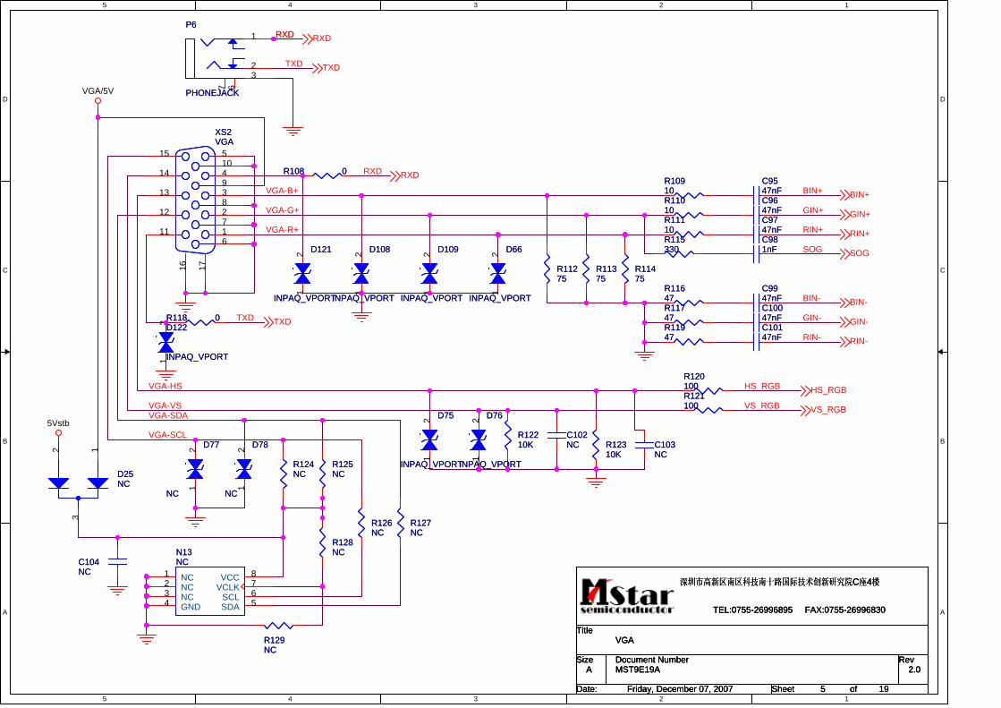
5 19Friday, December 07, 2007
Title
Size Document Number Rev
Date: Sheet of
深圳市高新区南区科技南十路国际技术创新研究院C座4楼
TEL:0755-26996895 FAX:0755-26996830
MST9E19A 2.0
VGA
A
5 19Friday, December 07, 2007
Title
Size Document Number Rev
Date: Sheet of
深圳市高新区南区科技南十路国际技术创新研究院C座4楼
TEL:0755-26996895 FAX:0755-26996830
MST9E19A 2.0
VGA
A
5 19Friday, December 07, 2007
C102NCC102NC
C9947nFC9947nFC10047nFC10047nF
R11475R11475
R11010R11010
D77
NC
D77
NC
12
D75
INPAQ_VPORT
D75
INPAQ_VPORT
12
R11275R11275
R125NCR125NC
D76
INPAQ_VPORT
D76
INPAQ_VPORT1
2
R12310KR12310K
D108
INPAQ_VPORT
D108
INPAQ_VPORT
12 D66
INPAQ_VPORT
D66
INPAQ_VPORT
12D109
INPAQ_VPORT
D109
INPAQ_VPORT
12
C103NCC103NC
R10910R10910
R120100R120100
N13NCN13NC
NC1NC2NC3GND4 SDA 5SCL 6VCLK 7VCC 8
R11375R11375
R108 0R108 0
R12210KR12210K
P6
PHONEJACK
P6
PHONEJACK
1
23
7 6
XS2VGAXS2VGA
5104938271
15
14
13
12
116
16 17
R11110R11110
C104NCC104NC
R118 0R118 0
R115330R115330
C981nFC981nF
D122
INPAQ_VPORT
D122
INPAQ_VPORT12
C9547nFC9547nF
R127NCR127NC
C9747nFC9747nF
R124NCR124NC
D121
INPAQ_VPORT
D121
INPAQ_VPORT1
2R11747R11747
R121100R121100
R126NCR126NC
D25NCD25NC
3
12 D78
NC
D78
NC
12
C9647nFC9647nF
R128NCR128NC
R129NCR129NC
R11647R11647
C10147nFC10147nF
R11947R11947
5
5
4
4
3
3
2
2
1
1
D D
C C
B B
A A
AV_VOUT
AV1-VAV1-VAV1-VAV1-VAV1-VAV1-VAV1-VAV1-VAV1-VAV1-VAV1-VAV1-VAV1-VAV1-VAV1-VAV1-V
CVBSOut
HD1_YINHD1_PBINHD1_PRIN
HD-VSW0
PC-RPC-R PC-Rin
Pr1
Y1
Pb1
HD1_PRIN
HD1_PBIN
HD1_YIN
AV2/SC1-R
S1-Cin
S1-Yin-
S1-YinS1-Y
S1-C
AV_Rout
AV_Lout
330_1_G330_1_B330_1_R
Pb1Pr1
Y1
SCB-
SCR-
SCG-
330_1_B330_1_R
330_1_GSCB+SCG+
SC_SOGSCR+
330_SOG
330_1_G 330_SOG
AV-SOG
HD1_YIN
AV-SOG
PC-L PC-Lin
SCART1-GSCART1-G
SCART1-R
AV-SOG
SCART1-B
SCART1-BSCART1-R
SCART1-G
Phone-MUTE
AMP-PLout
AMP-PRout
AV2/SC1-L
SCART1_MODE
SCART1_FB
AV2/SC1-V
Scart1_RoutAV2/SC1-RScart1_Lout
SC/RC_REDSC/RC_REDSC/RC_REDSC/RC_REDSC/RC_REDSC/RC_REDSC/RC_REDSC/RC_REDSC/RC_REDSC/RC_REDSC/RC_REDSC/RC_REDSC/RC_REDSC/RC_REDSC/RC_REDSC/RC_REDSC/RC_REDSC/RC_REDSC/RC_REDSC/RC_REDSC/RC_REDSC/RC_REDSC/RC_REDSC/RC_REDSC/RC_REDSC/RC_REDSC/RC_REDSC/RC_REDSC/RC_REDSC/RC_REDSC/RC_REDSC/RC_REDSC/RC_REDSC/RC_RED
SC/RC_GREENSC/RC_GREENSC/RC_GREENSC/RC_GREENSC/RC_GREENSC/RC_GREENSC/RC_GREENSC/RC_GREENSC/RC_GREENSC/RC_GREENSC/RC_GREENSC/RC_GREENSC/RC_GREENSC/RC_GREENSC/RC_GREENSC/RC_GREENSC/RC_GREENSC/RC_GREENSC/RC_GREENSC/RC_GREENSC/RC_GREENSC/RC_GREENSC/RC_GREENSC/RC_GREENSC/RC_GREENSC/RC_GREENSC/RC_GREENSC/RC_GREENSC/RC_GREENSC/RC_GREENSC/RC_GREENSC/RC_GREENSC/RC_GREENSC/RC_GREENSC/RC_GREENSC/RC_GREEN
SCART1_MODE SC_FS
SC_FSWSCART1_FB
AV2/SC1-VAV2/SC1-V
AV2/SC1-L
AV1-R
AV1-LAV1-L
Scart1_Lout
Scart1_Rout
AV1-Lin
AV1-Rin
AV2/SC1-V
AV2/SC1-Lin
AV2/SC1-Rin
AV1-Vin+
AV2/SC1-Vin+
SC/RC_BLUESC/RC_BLUE
SCART_VOUTSCART_VOUTSCART_VOUTSCART_VOUTSCART_VOUTSCART_VOUTSCART_VOUTSCART_VOUTSCART_VOUTSCART_VOUT
AV_VOUT
CVBSOut
SC/RC_BLUE
SC/RC_RED
SC/RC_GREEN
AV1-VAV1-VAV1-VAV1-VAV1-VAV1-VAV1-VAV1-V
AV1-L
5VPI+5VA
5VPI
5VPI
5VPI
5VPI
+5VA
5VPI
5VPI
AV2/SC1-Lin
AV2/SC1-Rin
AV2/SC1-Vin+
CVBSOut
PC-Rin
AV1-Vin+
AV1-Lin
AV1-Rin
S1-Cin
S1-Yin
S1-Yin-
Scart2_L
Scart2_R
HD-VSW0
SCR-
SCG-
SCB-
SCR+SCB+SCG+
SC_SOG
PC-Lin
SPDIF_OUT
SC2-LinDMP_DTV-L
SC2-RinDMP_DTV-R
SC1_VOUT6
Phone-MUTE
AMP-PLout
AMP-PRout
SCART_VOUT
SC_FSW
SC_FS
Scart1_L
Scart1_R
SC1_VOUT6
CVBSOut
SC/RC_RED
SC/RC_GREEN
SC/RC_BLUE
Title
Size Document Number Rev
Date: Sheet of
深圳市高新区南区科技南十路国际技术创新研究院C座4楼
TEL:0755-26996895 FAX:0755-26996830
MST9E19A 2.0
Video input
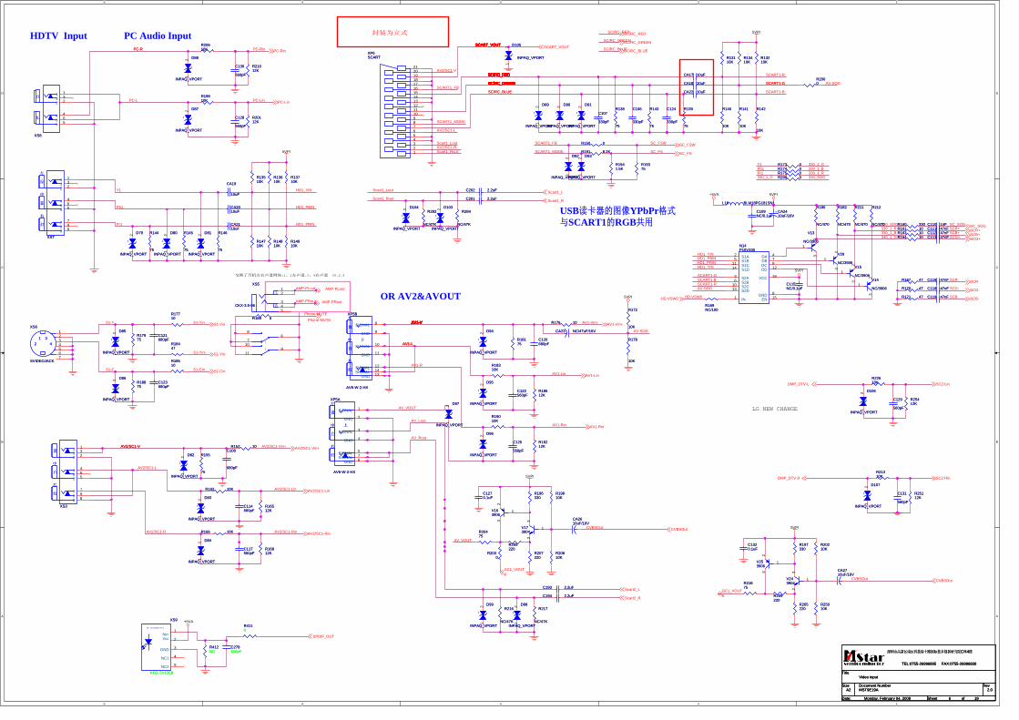
A2
6 19Monday, February 04, 2008
Title
Size Document Number Rev
Date: Sheet of
深圳市高新区南区科技南十路国际技术创新研究院C座4楼
TEL:0755-26996895 FAX:0755-26996830
MST9E19A 2.0
Video input
A2
6 19Monday, February 04, 2008
Title
Size Document Number Rev
Date: Sheet of
深圳市高新区南区科技南十路国际技术创新研究院C座4楼
TEL:0755-26996895 FAX:0755-26996830
MST9E19A 2.0
Video input
A2
6 19Monday, February 04, 2008
PC Audio InputHDTV Input
OR AV2&AVOUT
LG NEW CHANGE
USB读卡器的图像YPbPr格式与SCART1的RGB共用
封装为立式
交换了耳机左右声道网络;1、2左声道,3、4右声道 08.2.4
R25412KR25412K
L
R
XS5
CKX-3.5-06
L
R
XS5
CKX-3.5-06
2
3
1
45
67
8
910
11
C118 47nFC118 47nF
黄
白
红
中
右
XS3
黄
白
红
中
右
XS3
1 13 32 2
4 46 65 5
7 79 98 8
绿
蓝
红
左
中
右
XS7
绿
蓝
红
左
中
右
XS7
1 13 32 2
4 46 65 5
7 79 98 8
R155
75
R155
75
D97
INPAQ_VPORT
D97
INPAQ_VPORT
12
C131
560pF
C131
560pF
D91
INPAQ_VPORT
D91
INPAQ_VPORT
12
R150 0R150 0
C202 2.2uFC202 2.2uF
R169NC/100R169NC/100
R178
10K
R178
10K
R176 10R176 10
R20112KR20112K
V253906V253906
1
32
R22610KR22610K
D86
INPAQ_VPORT
D86
INPAQ_VPORT
12
R196330R196330
C119 47nFC119 47nF
R21310KR21310K
R212
NC/470
R212
NC/470
R138
75
R138
75
R144
75
R144
75
D93
INPAQ_VPORT
D93
INPAQ_VPORT
12
D103
INPAQ_VPORT
D103
INPAQ_VPORT
12
CA2110uFCA2110uF
C125
560pF
C125
560pF
CA2610uF/16VCA2610uF/16V
C116 47nFC116 47nF
C117560pFC117560pF
R412NCR412NC
CA2710uF/16VCA2710uF/16V
R170 47R170 47
C129
560pF
C129
560pF
R13710KR13710K
D83
INPAQ_VPORT
D83
INPAQ_VPORT
12
D94
INPAQ_VPORT
D94
INPAQ_VPORT
12
R207220R207220
R162 10KR162 10K
V29
NC/3906
V29
NC/39061
32
D92
INPAQ_VPORT
D92
INPAQ_VPORT
12
R211
NC/470
R211
NC/470
R18510R18510
+ CA2410uF/16V
+ CA2410uF/16V
R182
NC/470
R182
NC/470
R20475R20475
D104
INPAQ_VPORT
D104
INPAQ_VPORT
12
R13510KR13510K
R205220R205220
V13
NC/3906
V13
NC/39061
32
CA19
10uF
CA19
10uF
L16 BLM18PG181SN1L16 BLM18PG181SN1
D80
INPAQ_VPORT
D80
INPAQ_VPORT
12
IR Transmitter
XS9
KFO-TX13CB
IR Transmitter
XS9
KFO-TX13CB
1Nin
2Vcc
GND 3
NC1 4
NC2 5
R141
10K
R141
10K
R14910KR14910K
R216
NC/47K
R216
NC/47K
R14710KR14710K
R284
NC/47K
R284
NC/47K
CA18 10uFCA18 10uF
C194 2.2uFC194 2.2uF
D84
INPAQ_VPORT
D84
INPAQ_VPORT
12
C111 47nFC111 47nF
C106
330pF
C106
330pF
C1320.1uFC1320.1uF
R19010KR19010K
R19375R19375
C278100pFC278100pF
D99
INPAQ_VPORT
D99
INPAQ_VPORT
12
D88
INPAQ_VPORT
D88
INPAQ_VPORT
12
R152 10R152 10
R163 10R163 10
R18875R18875
C107
330pF
C107
330pF
V15
NC/3906
V15
NC/39061
32
C123680pFC123680pF
R2030
R2030
R171 47R171 47
R4110R4110
R19810KR19810K
V243904V243904
1
23
D107
INPAQ_VPORT
D107
INPAQ_VPORT
12
231
4
XS6
SVIDEOJACK
231
4
XS6
SVIDEOJACK
4321
567
C122560pFC122560pF
D82
INPAQ_VPORT
D82
INPAQ_VPORT
12
R139
75
R139
75
C121680pFC121680pF
R299 0R299 0
C124
330pF
C124
330pF
V163906V163906
1
32
R197330R197330
R1941.5KR1941.5K
V173904V173904
12
3
R16512KR16512K
C112 47nFC112 47nF
R175 0R175 0
V14
NC/3906
V14
NC/39061
32
D87
INPAQ_VPORT
D87
INPAQ_VPORT
12
D89
INPAQ_VPORT
D89
INPAQ_VPORT
12 R140
10K
R140
10K
C113 47nFC113 47nF
R173 0R173 0
C193 2.2uFC193 2.2uF
D81
INPAQ_VPORT
D81
INPAQ_VPORT
12
R13610KR13610K
R172
10K
R172
10K
R209220R209220
R166 10KR166 10K
R145
75
R145
75
R18612KR18612K
D95
INPAQ_VPORT
D95
INPAQ_VPORT
12
R2000R2000
R160 330R160 330
D85
INPAQ_VPORT
D85
INPAQ_VPORT
12
R13410KR13410K
XP6SCARTXP6SCART
2
4
6
8
10
12
14
16
18
20
1
3
5
7
9
11
13
15
17
19
21
R217
NC/47K
R217
NC/47K
CA2010uFCA2010uF
R21875R21875
C109NC/0.1uFC109NC/0.1uF
R174 0R174 0
C108
680pF
C108
680pF
R18447R18447
N14P15V330N14P15V330
S1A2S1B5S1C11S1D14
S2A3S2B6S2C10S2D13
IN1
DA 4DB 7DC 9DD 12
VCC 16
GND 8EN 15
R13210KR13210K
D96
INPAQ_VPORT
D96
INPAQ_VPORT
12
D90
INPAQ_VPORT
D90
INPAQ_VPORT
12
D105
INPAQ_VPORT
D105
INPAQ_VPORT
12
CA22 10uFCA22 10uF
黄
白
红
左
中
右
上
XP5A
AV6-W-2-HX
黄
白
红
左
中
右
上
XP5A
AV6-W-2-HX
SIGNAL 1
GND 2
GND 4
GND 6
SIGNAL 3
SIGNAL 5SIGNAL 7
D98
INPAQ_VPORT
D98
INPAQ_VPORT
12
R14810KR14810K
R17710R17710
R25010KR25010K
R20810KR20810K
R167 47R167 47
R283
NC/47K
R283
NC/47K
R16812KR16812K
R164 10R164 10
R13110KR13110K
D79
INPAQ_VPORT
D79
INPAQ_VPORT
12
R18175R18175
R142
10K
R142
10K
R189 0R189 0
R21012KR21012K
C114560pFC114560pF
C110 1nFC110 1nF
R180
NC/470
R180
NC/470
R20210KR20210K
CA17 10uFCA17 10uF
C1270.1uFC1270.1uF
R19910KR19910K
CA23 NC/47uF/16VCA23 NC/47uF/16V
D106
INPAQ_VPORT
D106
INPAQ_VPORT
12
C201 2.2uFC201 2.2uF
R18310KR18310K
C128
560pF
C128
560pF
R19212KR19212K
C120680pFC120680pF
R265220R265220
R25112KR25112K
R146
75
R146
75
R191 8.2KR191 8.2K
C130
560pF
C130
560pF
白
红
XS8
白
红
XS8
1 13 32 2
4 46 65 5
R161 10R161 10
R17975R17975
R143
75
R143
75
C115NC/0.1uFC115NC/0.1uF
黄
白
红
左
中
右
下
XP5B
AV6-W-2-HX
黄
白
红
左
中
右
下
XP5B
AV6-W-2-HX
SIGNAL 8
GND 9
GND 11
GND 13
SIGNAL 10
SIGNAL 12SIGNAL 14
R20610KR20610K
5
5
4
4
3
3
2
2
1
1
D D
C C
B B
A A
TV1-V
SIFPOUT
IF-AGC
SCL_EXTSDA_EXT
IF_TV
IF_TV
SDA_EXTSCL_EXT
IF-AGC
TV1-L/R
TV
SIFPOUT
TV1-Vin-
TV1-Vin+TV1-V
TV-SIFM
SCART_VOUT
TV
+5VA
AGND
AGND
+5VA
33V40V
+12V_all
+5VA
+5VA
5V-OUT
+5VA
AGND
+5V_all+5VA
+5VA
+5VA
+12V_all
+5VA5V-OUT
AGND
AGND
SCL_EXT 2SDA_EXT 2
TV1-Vin+
TV1-Vin-
TV-SIFP
TV-SIFM
SCART_VOUT 6
Title
Size Document Number Rev
Date: Sheet of
深圳市高新区南区科技南十路国际技术创新研究院C座4楼
TEL:0755-26996895 FAX:0755-26996830
MST9X88L 01A
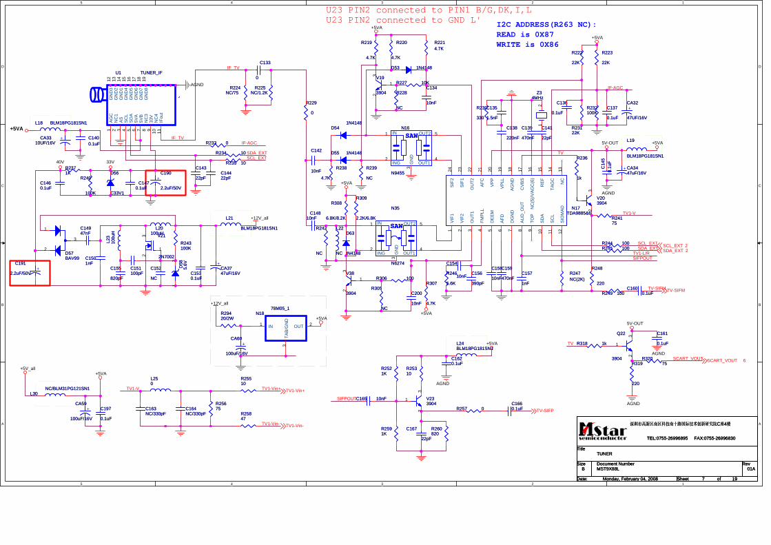
TUNER
B
7 19Monday, February 04, 2008
Title
Size Document Number Rev
Date: Sheet of
深圳市高新区南区科技南十路国际技术创新研究院C座4楼
TEL:0755-26996895 FAX:0755-26996830
MST9X88L 01A
TUNER
B
7 19Monday, February 04, 2008
Title
Size Document Number Rev
Date: Sheet of
深圳市高新区南区科技南十路国际技术创新研究院C座4楼
TEL:0755-26996895 FAX:0755-26996830
MST9X88L 01A
TUNER
B
7 19Monday, February 04, 2008
I2C ADDRESS(R263 NC):READ is 0X87WRITE is 0X86
U23 PIN2 connected to PIN1 B/G,DK,I,LU23 PIN2 connected to GND L'
R25310R25310
R23122KR23122K
C14947nFC14947nF
C158
10nF
C158
10nF
R2591KR2591K
D58
5.6VD58
5.6V
12
R222
22K
R222
22K
C138
220nF
C138
220nFC1400.1uFC1400.1uF
R318 1kR318 1k
+C190
2.2uF/50V
+C190
2.2uF/50V
C157
1nF
C157
1nF
V21
2N7002
V21
2N7002
1
32
L250L250
R235 10R235 10
R245 100R245 100
R232100KR232100K
C200
10nF
C200
10nF
U1 TUNER_IFU1 TUNER_IF
AGC
1N
C1
2AS
3SC
L4
SDA
55V
A6
5VB
7N
C3
833
V9
NC
410
IFou
t11
GN
D3
12G
ND
213
GN
D1
14G
ND
415
GN
D5
16G
ND
617
GN
D7
18G
ND
819
D63
IN4148
D63
IN4148
C14810nF
C14810nF
C161
0.1uF
C161
0.1uF
R305
NC
R305
NC
R238
4.7K
R238
4.7K
L24BLM18PG181SN1L24BLM18PG181SN1
R240
100K
R240
100K
C139
470nF
C139
470nF
+CA59
100uF/16V
+CA59
100uF/16V
R25510R25510
V203904V203904
1
32
Q22
3904
Q22
3904
1
32
R306 100R306 100
C197
0.1uF
C197
0.1uF
C1460.1uFC1460.1uF
R2214.7KR2214.7K
C151100pFC151100pF
C14422pFC14422pF
C14
50.
1uF
C14
50.
1uF
R228
NC
R228
NC
R32075
R32075
Z34MHz
Z34MHz
12
R25675R25675
+ CA3447uF/16V
+ CA3447uF/16V
C163NC/330pFC163NC/330pF R258
47R25847
L18 BLM18PG181SN1L18 BLM18PG181SN1
R242
NC
R242
NC
C1620.1uFC1620.1uF
L19
BLM18PG181SN1
L19
BLM18PG181SN1
L23
100u
HL2
310
0uH
R319
220
R319
220
R225NC/1.2K
R225NC/1.2K
C141
22pF
C141
22pF
R309
2.2K/6.8K
R309
2.2K/6.8K
R29420/2WR29420/2W
D55 1N4148D55 1N4148
C1530.1uFC1530.1uF
R227 10KR227 10K
C142
10nF
C142
10nF
R223
22K
R223
22K
C143
22pF
C143
22pF
SAW
N35
N6274
SAW
N35
N6274
2ING
4OUT1G
ND
3
5OUT21 IN
C165 10nFC165 10nF
R243100KR243100K
C1501nFC1501nF
R239
NC
R239
NC
C133
0
C133
0
D57BAV99D57BAV99
3
1
2
R24175R24175
D56
C33V1
D56
C33V1
V19
3904
V19
3904
1
23
R234 10R234 10
R220
4.7K
R220
4.7K
D541N4148
D541N4148
C156
390pF
C156
390pF
C155
820pF
C155
820pFV38
3904
V38
3904
1
32
R2371KR2371K
R308
6.8K/8.2K
R308
6.8K/8.2K
R257 0R257 0
R246
5.6K
R246
5.6K
+CA3310UF/16V
+CA3310UF/16V
C154
10nF
C154
10nF
L20100uH
L20100uH
R260820R260820
R244 100R244 100
+CA3747uF/16V
+CA3747uF/16V
C134
10nF
C134
10nF
C1470.1uF
C1470.1uF
C167
22pF
C167
22pF
R233 0R233 0
R236
1k
R236
1k
C152
NC
C152
NC
C1660.1uFC1660.1uF
R219
4.7K
R219
4.7K
R230
330
R230
330
R307
4.7K
R307
4.7K
N17TDA9885&6
N17TDA9885&6
DG
ND
7
TOP
9
VIF1
1
VIF2
2
REF
15
NC
(5)/V
AGC
(6)
16
DEE
M5
SCL
11
OU
T13
NC
13
AUD
_OU
T8
SDA
10
FMPL
L4
TAG
C14
AFD
6
SIO
MAD
12
CVB
S17
AGN
D18
VPLL
19
VPP
20
AFC
21
OU
T222
SIF1
23
SIF2
24
+CA32
47UF/16V
+CA32
47UF/16V
L22
NC
L22
NC
R248
220
R248
220
R224NC/75
R224NC/75
C135
1.5nF
C135
1.5nF
R2521KR2521K
R229
0
R229
0
D53 1N4148D53 1N4148
R247NC(2K)R247NC(2K)
L21
BLM18PG181SN1
L21
BLM18PG181SN1
C1600.1uF
C1600.1uF
+CA60
100uF/16V
+CA60
100uF/16V
R249 100R249 100
C137
0.1uF
C137
0.1uF
V233904V233904
1
32
L30NC/BLM31PG121SN1
L30NC/BLM31PG121SN1
SAWN16
N9455
SAWN16
N9455
2ING
4OUT1G
ND
3
5OUT21 IN
+C191
2.2uF/50V+
C191
2.2uF/50V
C136
0.1uF
C136
0.1uF
C164NC/330pFC164NC/330pF
C159
470nF
C159
470nF
N1878M05_1
N1878M05_1
IN1 OUT 2
TAB/
GN
D3
5
5
4
4
3
3
2
2
1
1
D D
C C
B B
A A
OP_VCC2
OP_VCC2
AUOut2-R
AUOut2-L
Scart1_R
Scart1_L
Scart2_L
Scart2_R
OP_VCC2
OP_VCC2
AUOut3-L
AUOut3-R
6VBuf2
+12V_all6VBuf2
+12V_all
OP_VCC2
OP_VCC2
Scart1_R
Scart1_L
AUOut2-R
AUOut2-L
AUOut3-R
AUOut3-L
Scart2_R
Scart2_L
Title
Size Document Number Rev
Date: Sheet of
MST9E19A 0.01
MSTAR
A3
8 19Monday, February 04, 2008
Title
Size Document Number Rev
Date: Sheet of
MST9E19A 0.01
MSTAR
A3
8 19Monday, February 04, 2008
Title
Size Document Number Rev
Date: Sheet of
MST9E19A 0.01
MSTAR
A3
8 19Monday, February 04, 2008
Audio OP(AUOUTL3/AUOUTR3; AUOUTL2/AUOUTR2)
R26810KR26810K
T1T1
W1W1
C1712.2uFC1712.2uF
R27933KR27933K
S4
NC/HOLE-V8
S4
NC/HOLE-V8
1
2
3
4
5
6
7
8
91111
1212
1313
1414
1515
16 16
17 17
18 18
QCLABELQCLABEL
C1680.1uFC1680.1uF
TXLABELTXLABEL
S2
NC/HOLE-V8
S2
NC/HOLE-V8
1
2
3
4
5
6
7
8
91111
1212
1313
1414
1515
16 16
17 17
18 18
R30147KR30147K
R28047KR28047K
R21447K
R21447K
C1702.2uFC1702.2uF
R26710KR26710K
S6
NC/HOLE-V8
S6
NC/HOLE-V8
1
2
3
4
5
6
7
8
91111
1212
1313
1414
1515
16 16
17 17
18 18
C177100pFC177100pF
S5
NC/HOLE-V8
S5
NC/HOLE-V8
1
2
3
4
5
6
7
8
91111
1212
1313
1414
1515
16 16
17 17
18 18
C1690.1uFC1690.1uF
R26347KR26347K
C1742.2uFC1742.2uF
R27547KR27547K
R30247KR30247K
R261100R261100
R26410KR26410K
C176100pFC176100pF
CA38100uF/16VCA38100uF/16V
-
+
N20ATL062
-
+
N20ATL062
3
21
84
-
+
U20ABA4558
-
+
U20ABA4558
3
21
84
R262 47KR262 47K
R27133KR27133K
-
+
N20B
TL062
-
+
N20B
TL062
5
67
84
R26910KR26910K
-
+
U20BBA4558
-
+
U20BBA4558
5
67
84
C1752.2uFC1752.2uF
R27633KR27633K
S1
NC/HOLE-V8
S1
NC/HOLE-V8
1
2
3
4
5
6
7
8
91111
1212
1313
1414
1515
16 16
17 17
18 18
R21547KR21547K
S3
NC/HOLE-V8
S3
NC/HOLE-V8
1
2
3
4
5
6
7
8
91111
1212
1313
1414
1515
16 16
17 17
18 18
C172100pFC172100pF
R26633KR26633K
R277100R277100
CA39100uF/16VCA39100uF/16V
C173100pFC173100pF
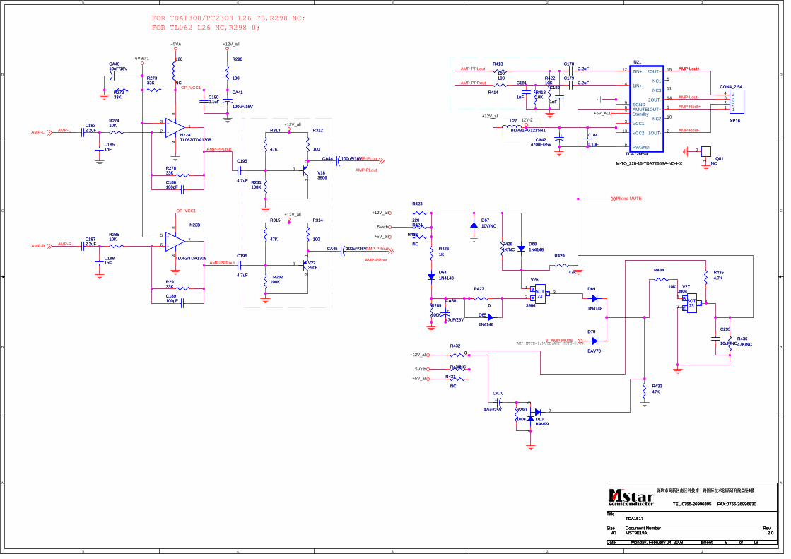
5
5
4
4
3
3
2
2
1
1
D D
C C
B B
A A
OP_VCC1
AMP-PRout
OP_VCC1
AMP-L
AMP-R
AMP-Lout+AMP-Lout+
AMP-Lout-
AMP-Rout+
AMP-Rout-
AMP-PPLout
AMP-PLout
AMP-PPRout
AMP-PPLout
AMP-PPRout
+5VA
6VBuf1
12V-2+12V_all
+12V_all
+12V_all
+12V_all
+5V_ALL
+5V_all
+12V_all
5Vstb
5Vstb
+5V_all
+12V_all
AMP-L
AMP-R
AMP-PLout
AMP-PRout
AMP-MUTE2
Phone-MUTE
Title
Size Document Number Rev
Date: Sheet of
深圳市高新区南区科技南十路国际技术创新研究院C座4楼
TEL:0755-26996895 FAX:0755-26996830
MST9E19A 2.0
TDA1517
A3
9 19Monday, February 04, 2008
Title
Size Document Number Rev
Date: Sheet of
深圳市高新区南区科技南十路国际技术创新研究院C座4楼
TEL:0755-26996895 FAX:0755-26996830
MST9E19A 2.0
TDA1517
A3
9 19Monday, February 04, 2008
Title
Size Document Number Rev
Date: Sheet of
深圳市高新区南区科技南十路国际技术创新研究院C座4楼
TEL:0755-26996895 FAX:0755-26996830
MST9E19A 2.0
TDA1517
A3
9 19Monday, February 04, 2008
FOR TDA1308/PT2308 L26 FB,R298 NC;FOR TL062 L26 NC,R298 0;
AMP-MUTE=1,MUTE;AMP-MUTE=0,ON;
L26
NC
L26
NC
CA44 100uF/16VCA44 100uF/16V
R314
100
R314
100
Q01NC
Q01NC1
2
-
+
N22B
TL062/TDA1308
-
+
N22B
TL062/TDA1308
5
67
84
N21
TDA7266sa
M-TO_220-15-TDA7266SA-NO-HX
N21
TDA7266sa
M-TO_220-15-TDA7266SA-NO-HX
1IN+4
1OUT- 2
1OUT+ 1
2OUT+ 15
2OUT- 14
2IN+12
AMUTE6
VCC13
PWGND8
SGND9
VCC213
Standby7
NC1 5
NC2 10
NC3 11
R313
47K
R313
47K
D10BAV99D10BAV99
3
2
1
R430NCR430NC
C186100pFC186100pF
R4261KR4261K
R43647K/NCR43647K/NC
R431
NC
R431
NC
R4281K/NCR4281K/NC
C293
10uF/NC
C293
10uF/NC
R41810KR41810K
V183906V183906
1
32
R312
100
R312
100
D70
BAV70
D70
BAV70
R423
220
R423
220
+
CA70
47uF/25V
+
CA70
47uF/25V
D65
1N4148
D65
1N4148
R27833KR27833K
C189100pFC189100pF
C1851nFC1851nF
R432
0
R432
0
C181
1nF
C181
1nF
D681N4148D681N4148
R4354.7KR4354.7K
R315
47K
R315
47K
D69
1N4148
D69
1N4148
CA4010uF/16VCA4010uF/16V
XP16
CON4_2.54
XP16
CON4_2.54
11 22 33 44CA41
100uF/16V
CA41
100uF/16V
R27333KR27333K
R290
100K
R290
100K
CA45 100uF/16VCA45 100uF/16V
+
CA50
47uF/25V
+
CA50
47uF/25V
C1792.2uF
C1792.2uF
C182
1nF
C182
1nF
R27410KR27410K
R28510KR28510K
C1782.2uF
C1782.2uF
R29133KR29133K
R289
100K
R289
100K
C1872.2uFC1872.2uF
R427
0
R427
0
-
+
N22ATL062/TDA1308
-
+
N22ATL062/TDA1308
3
21
84
R424
NC
R424
NC
C196
4.7uF
C196
4.7uF
C1832.2uFC1832.2uF
C1800.1uFC1800.1uF
R282100K
R282100K
R434
10K
R434
10K
D641N4148D641N4148
R42210KR42210K
R413
100
R413
100
L27
BLM31PG121SN1
L27
BLM31PG121SN1
E
BCSOT
23
V273904
E
BCSOT
23
V2739041
32
R425
NC
R425
NC
D6710V/NCD6710V/NC
C184
0.1uF
C184
0.1uF
R298
100
R298
100
E
BCSOT
23
V26
3906E
BCSOT
23
V26
3906
13
2
R27233KR27233K
C195
4.7uF
C195
4.7uF
C1881nFC1881nF V22
3906V223906
1
32 R429
47K
R429
47K
R43347KR43347K
R414
100
R414
100
R281100KR281100K
+CA42
470uF/35V
+CA42
470uF/35V
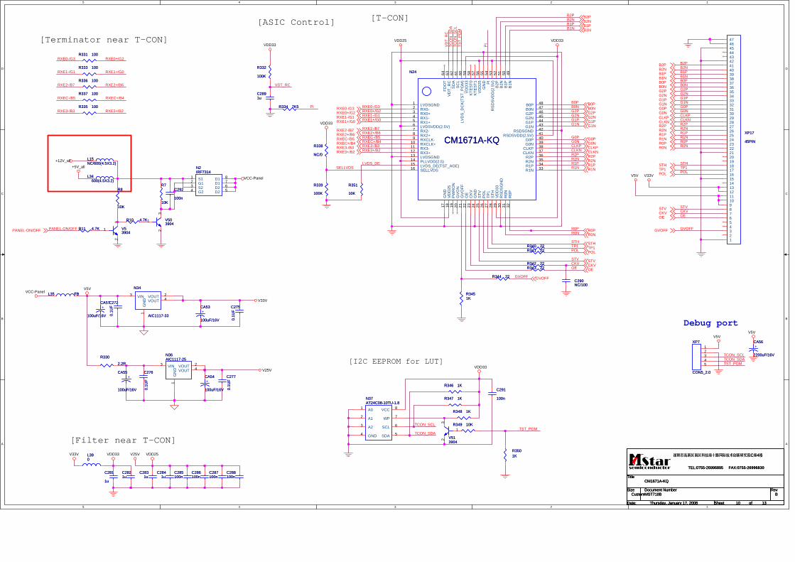
5
5
4
4
3
3
2
2
1
1
D D
C C
B B
A AVD
T_R
C
GVOFF
TCO
N_S
DA B1N
PI
VDT_RC
B1PB2N
PI
B2P
G1NG1PG2NG2PB0NB0P
R1NR1PR2NR2P
G0NG0P
R0PR0N
SELLVDS
CLKN
TCO
N_S
CL
STH
CLKP
STV
TST_
PGM
RXE0-/G3RXE0+/G2
OE
RXE1-/G1RXE1+/G0
CKV
TP1
RXE2-/B7RXE2+/B6RXEC-/B5RXEC+/B4
RXE1+/G0RXE1-/G1
RXE2-/B7
RXE0+/G2
RXE2+/B6
RXE0-/G3
POL
RXE3-/B3 RXE3+/B2
RXEC-/B5 RXEC+/B4
RXE3-/B3RXE3+/B2
TST_PGMTCON_SCL
TCON_SDA
B2PB2NB1PB1NB0PB0NG2PG2NG1PG1NG0PG0NCLKPCLKNR2PR2NR1PR1NR0PR0N
STHTP1POL
STVCKVOE
GVOFF
TCON_SDATCON_SCL
TST_PGM
PANEL-ON/OFF
LVDS_DE
VDD25
VDD25
VDD33VDD33
V33V V25VVDD33
VDD33
VDD33
V33VV5V
V5V
V5V
V33V
VCC-Panel
V25V
+5V_all
VCC-Panel
V5V
+12V_all
STV
GVOFF
B2P
B1NB1PB2N
TP1
G2P
CLKPG0NG0P
B0NB0P
G1N
CLKN
G1PG2N
POL
STH
R2PR2NR1PR1N
CKV
R0PR0N
OE
B1P
G1P
G2P
B2P
B0P
G0P
R1P
R0P
G2N
R0N
R1N
R2PR2N
G1N
G0N
B0N
B2N
B1N
CLKPCLKN
STHTP1POL
STV
OECKV
GVOFF
RXE0+/G2
RXEC+/B4
RXE1+/G0
RXE2-/B7RXE2+/B6RXEC-/B5
RXE3-/B3RXE3+/B2
RXE1-/G1
RXE0-/G3
PANEL-ON/OFF
Title
Size Document Number Rev
Date: Sheet of
深圳市高新区南区科技南十路国际技术创新研究院C座4楼
TEL:0755-26996895 FAX:0755-26996830
MST718B B
CM1671A-KQ
Custom
10 13Thursday, January 17, 2008
Title
Size Document Number Rev
Date: Sheet of
深圳市高新区南区科技南十路国际技术创新研究院C座4楼
TEL:0755-26996895 FAX:0755-26996830
MST718B B
CM1671A-KQ
Custom
10 13Thursday, January 17, 2008
Title
Size Document Number Rev
Date: Sheet of
深圳市高新区南区科技南十路国际技术创新研究院C座4楼
TEL:0755-26996895 FAX:0755-26996830
MST718B B
CM1671A-KQ
Custom
10 13Thursday, January 17, 2008
[T-CON]
[Filter near T-CON]
[Terminator near T-CON]
[I2C EEPROM for LUT]
[ASIC Control]
Debug port
R342 22R342 22
C272
0.1U
F
C272
0.1U
FR335 100R335 100
N37AT24C08-10TU-1.8N37AT24C08-10TU-1.8
VCC 8
A12 WP 7
SCL 6
SDA 5GND4
A23
A01
N2IRF7314N2IRF7314
S11G12S23G24
D1 8D1 7D2 6D2 5
R333 100R333 100
C286100nC286100n
R336 100R336 100
N24
CM1671A-KQ
N24
CM1671A-KQ
RS
DS
GN
D30
STH
28
G1N 43
G0N 39
VD
D25
56K
TES
T157
KTE
ST0
58
VD
D25
18
RSDSVDD(2.5V) 41
R1N 33
CLKN 37
B1N
49
VD
T_R
C63
PO
L26
R2N 35
VD
D33
29
SELLVDS16
G2P 46
CK
V23
B0P 48
B1P
50
OE
22
R0P
32
GV
OFF
21V
DD
3359
SD
A62
RS
DS
VD
D(2
.5V
)53
GN
D17
G1P 44
SC
L61
G0P 40
CLKP 38
B2N
51
RSDSGND 42
GN
D24
R1P 34
TP1
27
FDO
T64
R2P 36
G2N 45
GN
D55
PI
54
PW
RO
N19
GV
ON
20
STV
25
B0N 47
B2P
52
R0N
31
LVDSGND1RX0-2RX0+3RX1-4RX1+5LVDSVDD(2.5V)6RX2-7RX2+8RXCLK-9RXCLK+10RX3-11RX3+12LVDSGND13PLLVDD(2.5)14LVDS_DE(TST_AGE)15
LVD
S_D
CK
(TS
T_P
GM
)60
V513904V513904
1
23
R340 22R340 22
+CA55
100uF/16V
+CA55
100uF/16V
C290NC/100C290NC/100
R347 1KR347 1K
R341 22R341 22
L390L390
L15NC/600(4.5X3.2)L15NC/600(4.5X3.2)
R337 100R337 100
V53904V53904
1
23
C291
100n
C291
100n
C292
100n
C292
100n
R332
100K
R332
100K
L34600(4.5X3.2)
L34600(4.5X3.2)
C281
1u
C281
1u
N34
AIC1117-33
N34
AIC1117-33
GN
D1
VOUT 2VIN3VOUT 4
R338
NC/0
R338
NC/0
R339
100K
R339
100K
L35 FBL35 FB
C277
0.1U
F
C277
0.1U
F
R343 22R343 22
R10 4.7KR10 4.7K
R346 1KR346 1K
+CA57
100uF/16V
+CA57
100uF/16V
C2891uC2891u
R331 100R331 100
R3501KR3501K
R11 4.7KR11 4.7K
C2841u
C2841u
R348 1KR348 1K
R349 10KR349 10K
R3451KR3451K
C275
0.1U
F
C275
0.1U
F
XP7
CON5_2.0
XP7
CON5_2.0
12345
R330
2.2R
R330
2.2R
R8
10K
R8
10K
C288100nC288100n
C2831u
C2831u
C276
0.1U
F
C276
0.1U
F
C287100nC287100n
V503904V503904
1
23
R351
10K
R351
10K
R344 22R344 22
N36AIC1117-25N36AIC1117-25
GN
D1
VOUT 2VIN3VOUT 4
C285100nC285100n
R7
10K
R7
10K
+CA53
100uF/16V
+CA53
100uF/16V
XP17
45PIN
XP17
45PIN
1234567891011121314151617181920212223242526272829303132333435363738394041424344454647
R334 7K5R334 7K5
C2821uC2821u
+CA54
100uF/16V
+CA54
100uF/16V
+CA56
2200uF/16V
+CA56
2200uF/16V