Embed Size (px)
Citation preview

Lithography Explored
Leslie ChapmanJune 27, 2007

TEKS Objectives
• (A) plan and implement investigative procedures including asking questions, formulating testable hypotheses, and selecting equipment and technology.
• (B) identify uses of electromagnetic waves in various technological applications, such as fiber optics, optical scanners, microwaves, and microfabrication.
• (C) communicate valid conclusions.
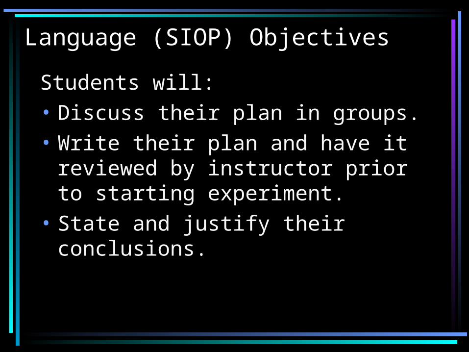
Language (SIOP) Objectives
Students will:• Discuss their plan in groups. • Write their plan and have it
reviewed by instructor prior to starting experiment.
• State and justify their conclusions.

THE ASSIGNMENT
• Design a CD label for your favorite music artist using the UV Lithography technique.

Lithography Process
Prepare Substrate
Apply Photoresist
Develop
SoftbakeExpose
Post Exposure
Bake

Background Information
• Process through which very small 3-D features can be produced.
• Involves a series of steps that creates successive layers of materials.
Substrate (CD)
Positive Photoresist
(S-1813)
UV Light
Mask (transparency with design)
Substrate – process starts here. Silicon is the preferred material.Photoresist – a chemical that is sensitive to radiation (i.e. light) and whose properties (i.e. solubility) are changed when exposed to radiation.
The photoresist is exposed to radiation using the mask which contains a pattern that is transferred to the top layer.

Lithography Process
• Create a mask.• Start with a
substrate• Cover surface
with photoresist.
• Soft bake• Expose the
wafer to energy
• Develop the wafer

Photo
Lithography
Changing light source = type of lithography
Types of
UV Light
PhotoX-ray
X-ray
UV

Industrial Uses of Lithography
• Electronics and Telecommunications– Television, radio and
printers– Calculators and watches– Video cameras and
computers (microprocessor)
– Cell phones and waveguides
• Aviation and Aerospace– Airplanes, meterology
equipment and Spaceships
• Automobile– Cars (microchips
trigger inflation of air bag)
– Traffic light (signals)
• Pharmaceutical– Lab on a chip– Portable blood
analyzers (microchip-based sensing devices)

Applications of Lithography• A truly amazing MEMS
device. It is a sophisticated MEMS Thermal Actuator
• Complex MEMS Ratchet Mechanism

Incredible MEMS Clutch mechanism. This is actually a complex device that required a working clutch mechanism. Gears are 50 microns across.

An early micromotor built in the SUMMiT technology. For size comparison a microscopic dust mite is shown on top.

Applications of X-ray Lithography
Examples [9][9] http://www.ca/sandia.gov/liga/tech.html
Micro gears
Micro motor core
Switching mechanism

THE ASSIGNMENT
• Work in pairs to Design a CD label for your favorite music artist using the UV Lithography technique.
• Each pair will design two CD labels– One CD will be the control.– The other CD will be varied (photoresist or
exposure time).• State and justify the impact your
variation had on the final product.• Constraints
– Design must be drawn in black ink only.– Design must be able to fit on a CD.

• Create a design• Transfer the design to
transparency paper (inkjet or copy machine)
• Keep the transparency clean

1. Prepare Substrate
• Clean with isopropanol
• Bake at 115°C for 60 seconds
Prepare Substrate
Apply Photoresist
Develop
SoftbakeExpose
Post Exposure
Bake

2. Apply Positive Photoresist
• Photoresist is spin coated on to CD
• Students will dip CD in S-1813 to get even spread.
• Effective for λ 340 – 450 nm
Prepare Substrate
Apply Photoresist
Develop
SoftbakeExpose
Post Exposure
Bake

3. Softbake
• 115°C for 60 seconds
• Complete when photoresist is hard to the touch.
• Temp. range: 5 – 550°C (41 - 1022°F)
Prepare Substrate
Apply PhotoresistDevelop
SoftbakeExpose
Post Exposure
Bake

4. Expose• Long wave UV mini
lamp (Intensity = 230 μW/cm2)
• Exposure time: 25 seconds
Prepare Substrate
Apply Photoresist
Develop
SoftbakeExpose
Post Exposure
Bake

5. Develop• Immerse wafer in
solution for 40 – 60 seconds. Agitation is recommended.
• Quickly remove the wafer from the developer bath and rinse with deionized water bath for 30 seconds (using the wafer holder).
• Place the wafer on a clean room wipe.
• Dry the wafer holder.
Prepare Substrate
Apply Photoresist
Develop
SoftbakeExpose
Post Exposure
Bake

6. Post Exposure Bake
• Bake at 115°C for 60 seconds
• Set a hotplate to the required temperature.
• Place the wafer on the hotplate, start timing.
• When the time is up, remove the wafer.

• Aprons, gloves and safety goggles required at all times.
• UV goggles required during exposure.
• The more photoresist present, the longer the bake time.
Reminders
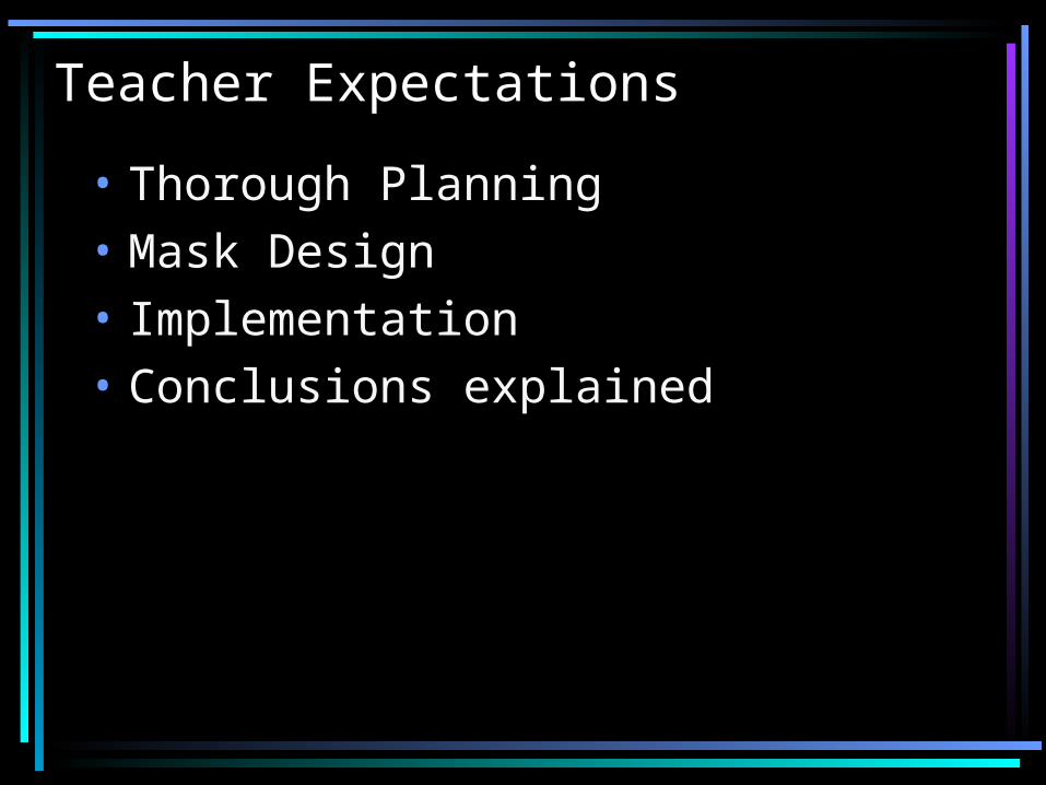
Teacher Expectations
• Thorough Planning• Mask Design• Implementation• Conclusions explained

Points (for Instructor) to Consider
• Give time limit on mask design. Students may design on computer or by hand. Intricacy of design may impact exposure quality.
• Thickness of photoresist impacts bake time• Exposure time could impact image seen on
substrate• Substrate surface must be very clean• Students must wear UV goggles when
operating UV lamp

Time Frame
Three class periods (50 minutes each)
1. Day One – Background Info, Mask Design, Substrate Preparation,
2. Day Two – Wafer Preparation, Apply photoresist, Softbake
3. Day Three – Expose, Develop, State Conclusions

THANK YOU
• Dr. Kim• Mr. Creary• Dr. Conkey• Dr. Srinivasa• Mr. Derry• Colleagues in the program


![2 LASER INTERFERENCE LITHOGRAPHY - uni-halle.de · 2 LASER INTERFERENCE LITHOGRAPHY (LIL) 9 2 LASER INTERFERENCE LITHOGRAPHY (LIL) Laser interference lithography [3~22] (LIL) is a](https://img.pdfslide.net/doc/110x75/5eae180eecc7e273a41a4e88/2-laser-interference-lithography-uni-hallede-2-laser-interference-lithography.jpg)