Embed Size (px)
Citation preview
1
Lithography
Prof. Yosi Shacham-Diamand
Fall 2004
33rdrd lecture: introductionlecture: introduction

2
List of contentFundamental principlesCharacteristics parametersExposure systems
3
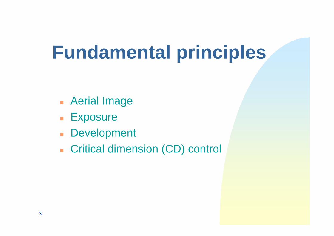
Fundamental principles
Aerial ImageExposure DevelopmentCritical dimension (CD) control
4
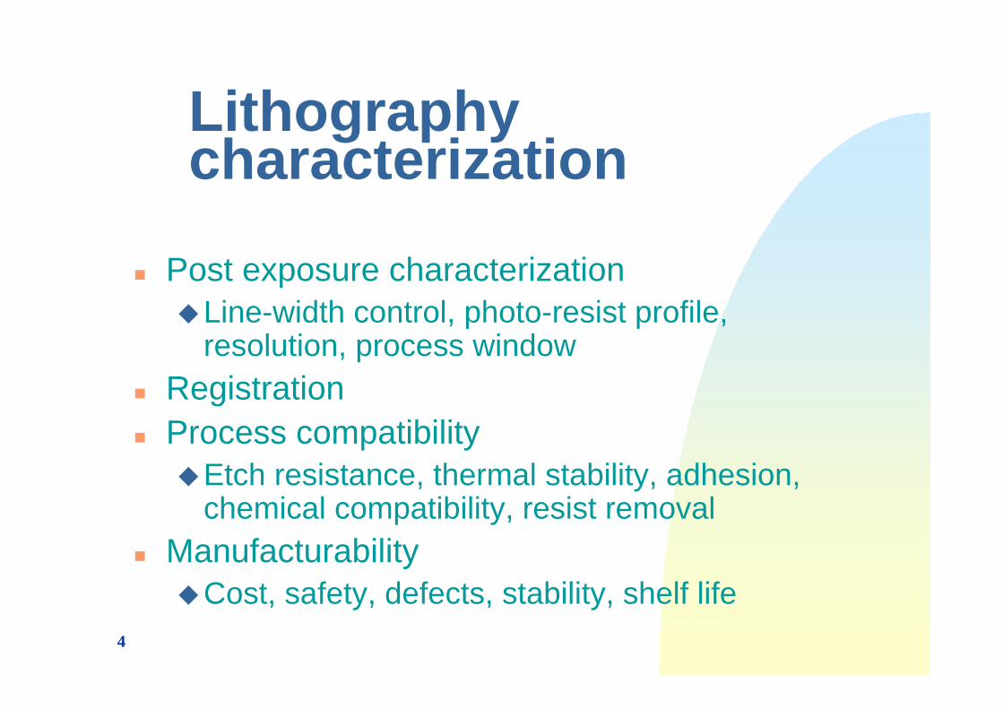
Lithography characterization
Post exposure characterizationLine-width control, photo-resist profile, resolution, process window
RegistrationProcess compatibility
Etch resistance, thermal stability, adhesion, chemical compatibility, resist removal
ManufacturabilityCost, safety, defects, stability, shelf life
5
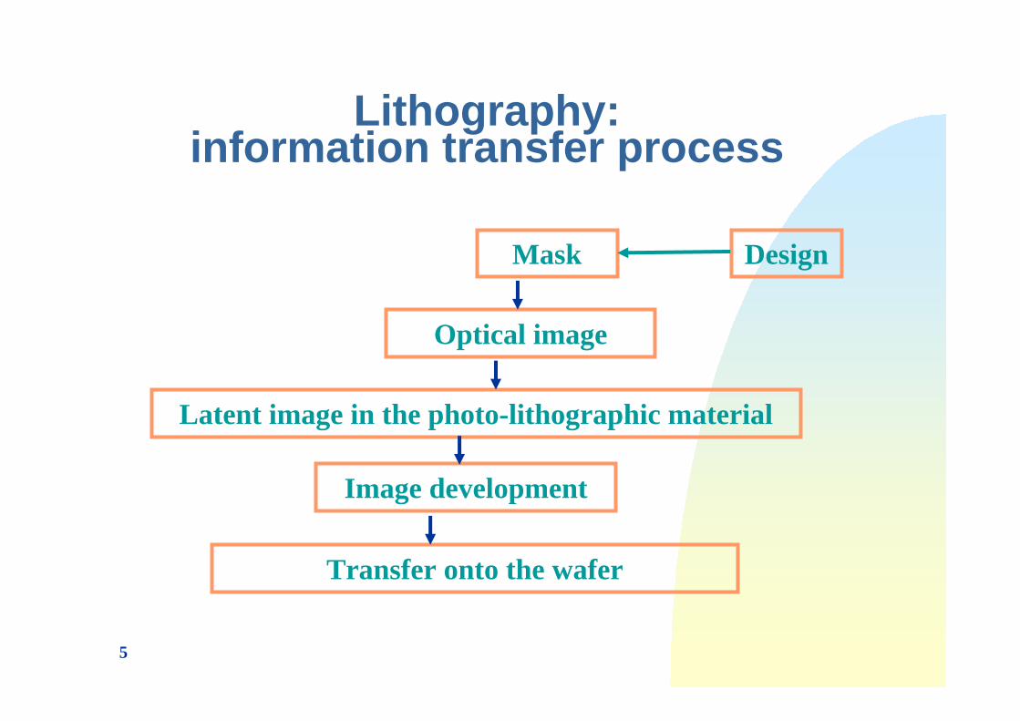
Lithography: information transfer process
Mask
Optical image
Latent image in the photo-lithographic material
Image development
Transfer onto the wafer
Design
6
7
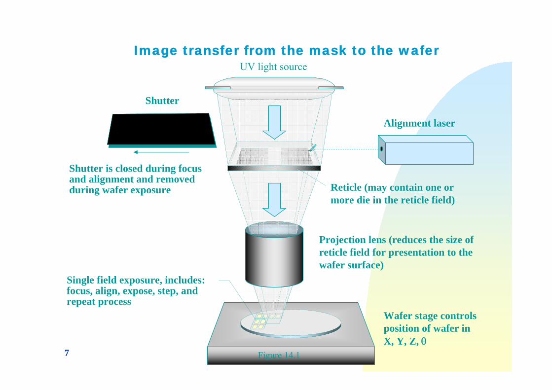
Image transfer from the mask to the wafer
Single field exposure, includes: focus, align, expose, step, and repeat process
UV light source
Reticle (may contain one or more die in the reticle field)
Shutter
Wafer stage controls position of wafer in X, Y, Z, θ
Projection lens (reduces the size of reticle field for presentation to the wafer surface)
Shutter is closed during focus and alignment and removed during wafer exposure
Alignment laser
Figure 14.1

8
9
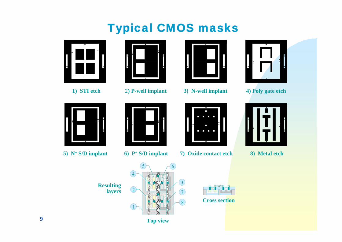
Typical CMOS masks
4) Poly gate etch1) STI etch 2) P-well implant 3) N-well implant
8) Metal etch5) N+ S/D implant 6) P+ S/D implant 7) Oxide contact etch
Top view
1
23
45
7
6
8 Cross section
Resulting layers
10
11
12
13
14
15
16
17
18
19
20
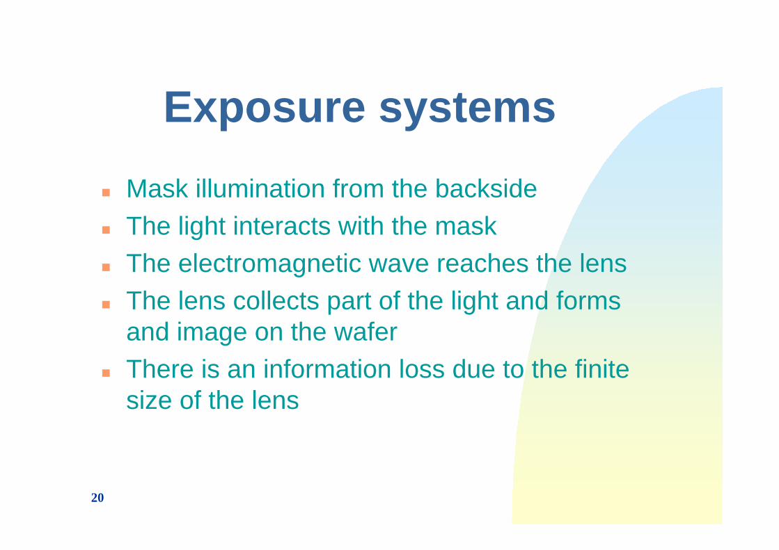
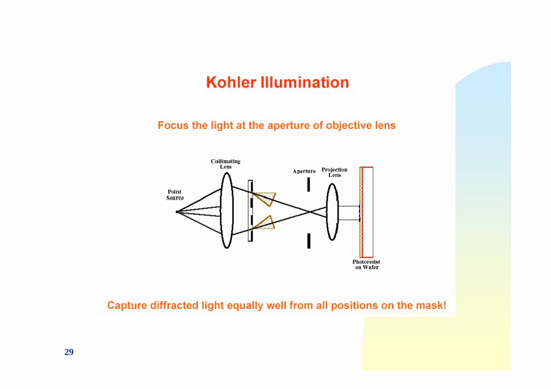
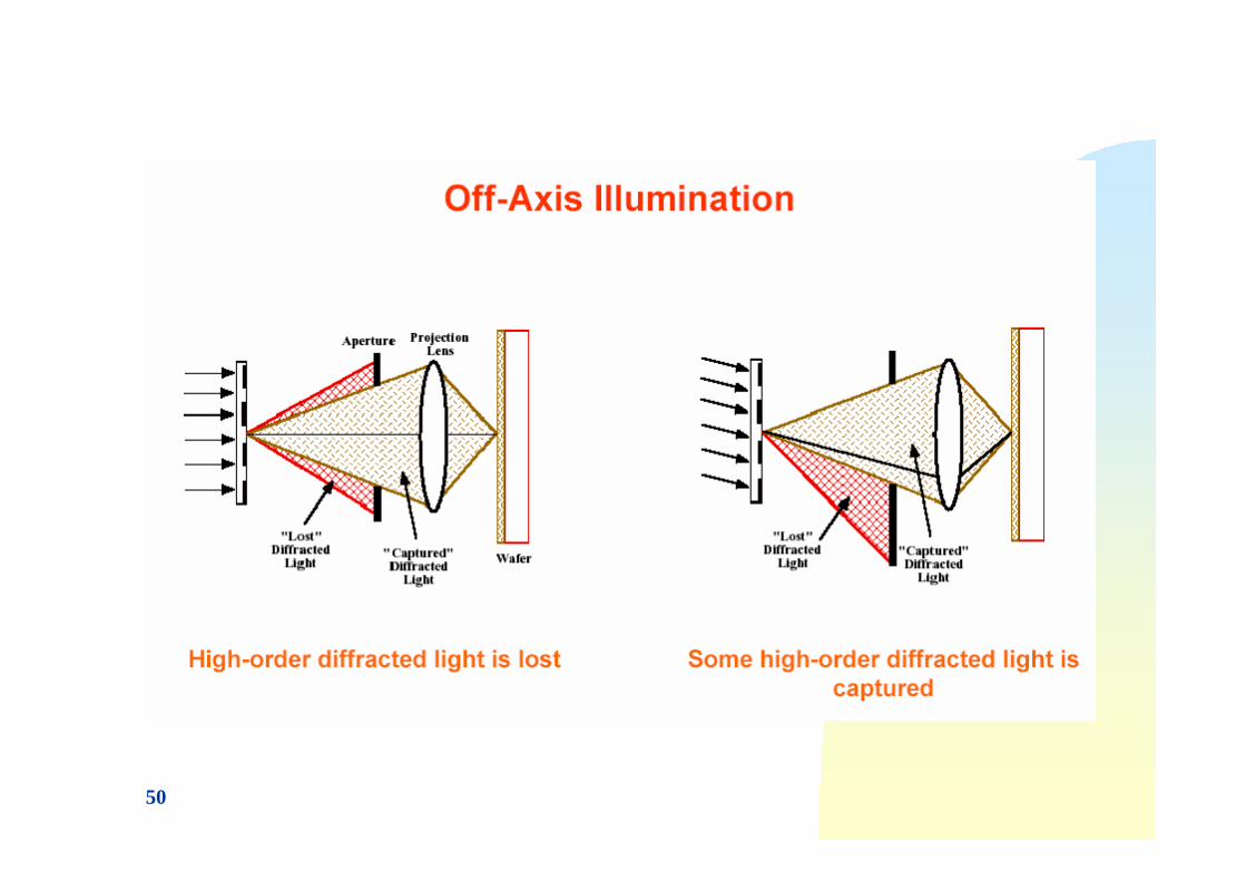
Exposure systemsMask illumination from the backsideThe light interacts with the maskThe electromagnetic wave reaches the lensThe lens collects part of the light and forms and image on the waferThere is an information loss due to the finite size of the lens
21
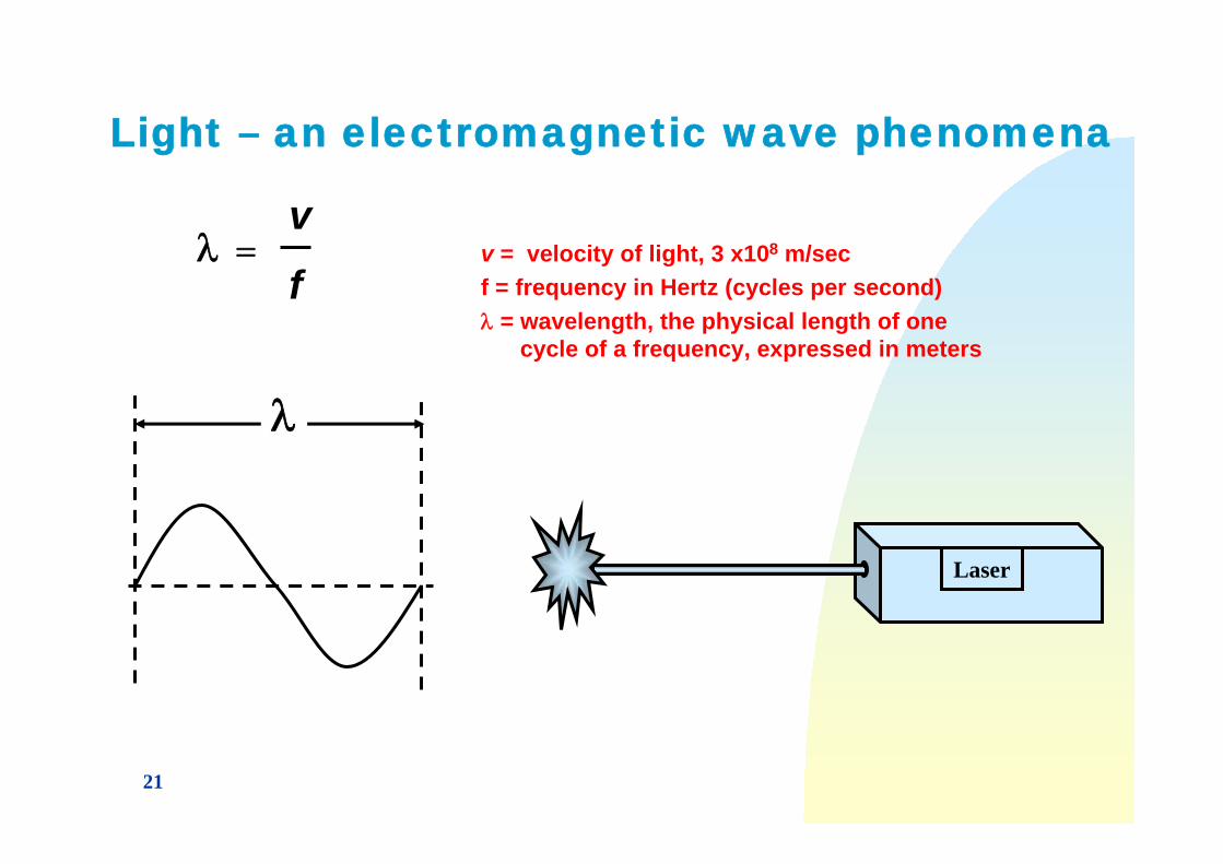
Light – an electromagnetic wave phenomena
λ
λ =vf
Laser
v = velocity of light, 3 x10⁸ m/secf = frequency in Hertz (cycles per second)λ = wavelength, the physical length of one
cycle of a frequency, expressed in meters
22
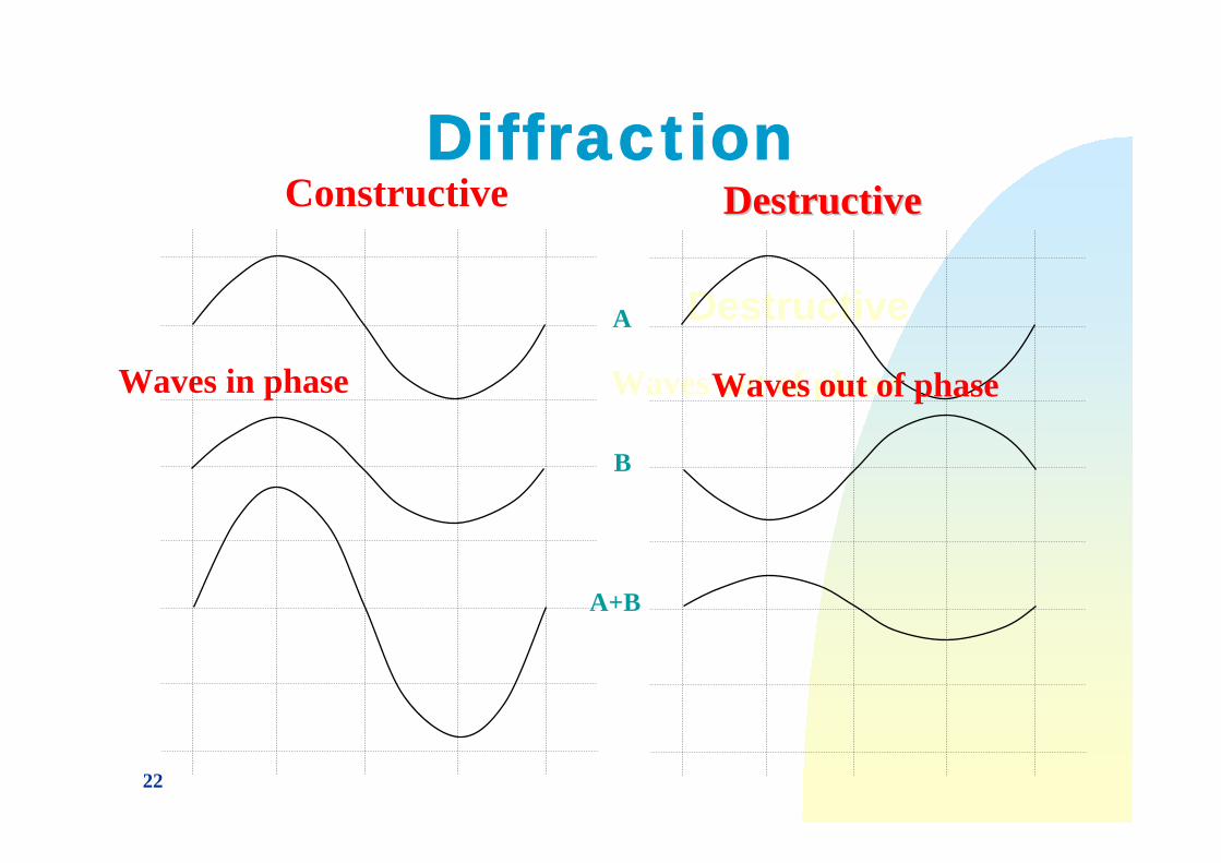
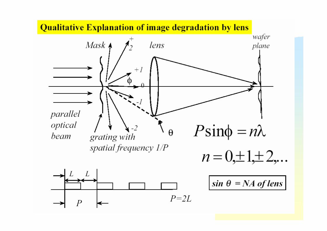
Diffraction
A
B
A+B
Waves in phase Waves out of phase
Constructive
Destructive
DestructiveDestructive
Waves out of phase
23
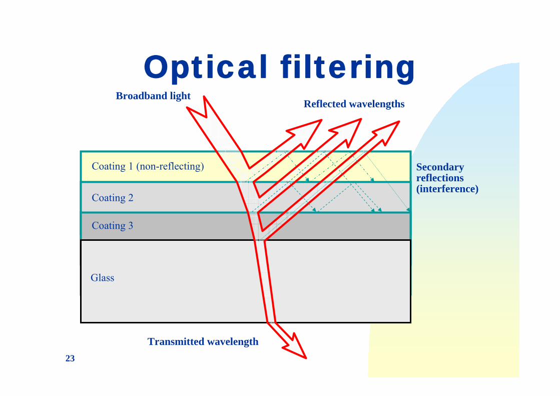
Optical filtering
Secondary reflections (interference)
Coating 1 (non-reflecting)
Coating 3
Glass
Coating 2
Reflected wavelengths
Transmitted wavelength
Broadband light
24
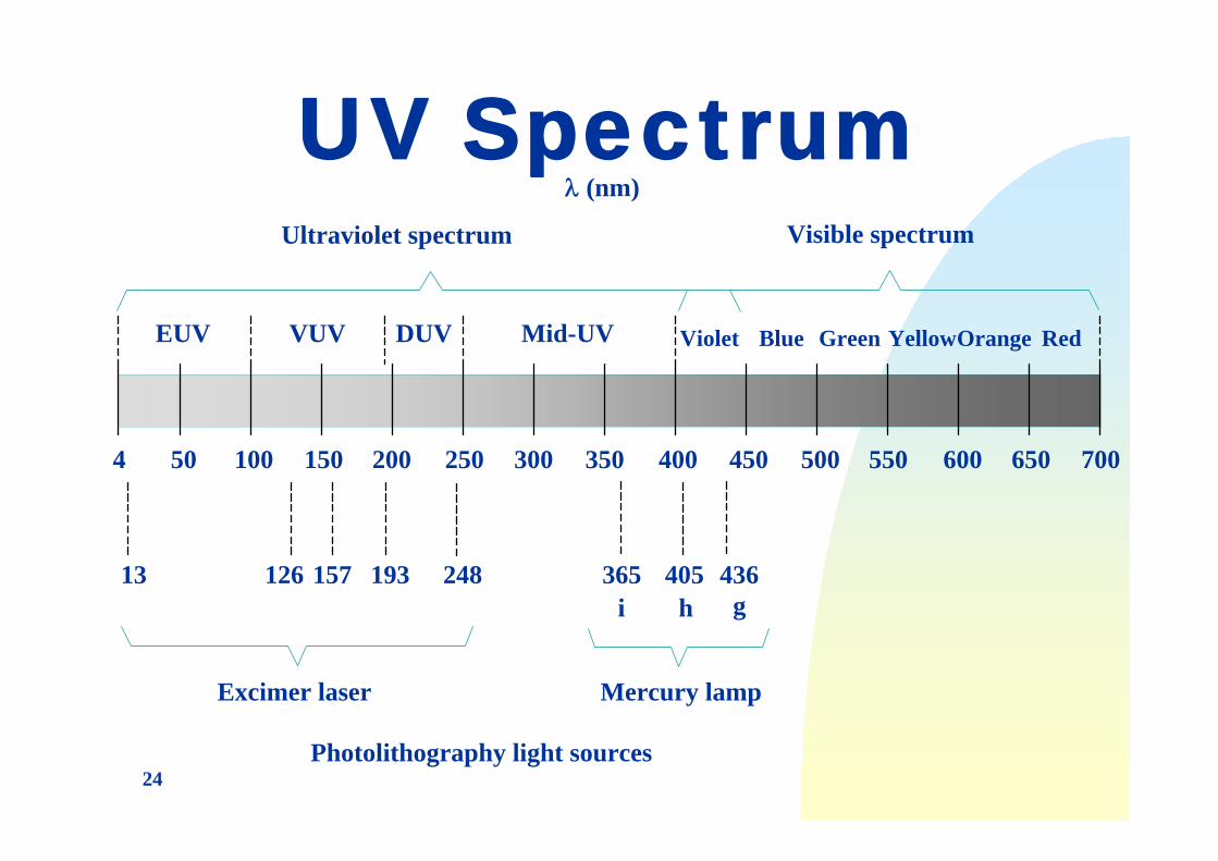
Spectrum UVλ (nm)
7004 550 600 65050045040035030025020015010050
Ultraviolet spectrum Visible spectrum
Mercury lampExcimer laser
Photolithography light sources
ghi365 40524819313 436157126
Violet RedBlue Green YellowOrangeMid-UVEUV DUVVUV
25
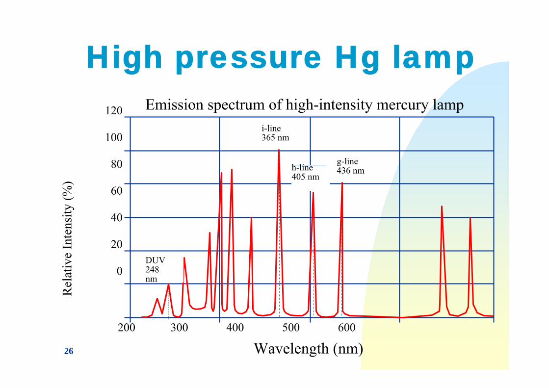
26
High pressure Hg lamp120
100
80
60
40
20
0
200 300 400 500 600
Wavelength (nm)
Rel
ativ
e In
tens
ity (%
)
h-line405 nm
g-line436 nm
i-line365 nm
DUV248 nm
Emission spectrum of high-intensity mercury lamp

27
UV Light Wavelength (nm) Descriptor CD Resolution (µm)
436 g-line 0.5405 h-line 0.4365 i-line 0.35248 Deep UV
(DUV)0.25
High pressure Hg lamp
28
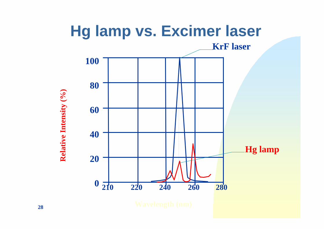
100
80
60
40
20
0
Rel
ativ
e In
tens
ity (%
)
KrF laser
280210 240 260220
Wavelength (nm)
Hg lamp
Hg lamp vs. Excimer laser
29
30
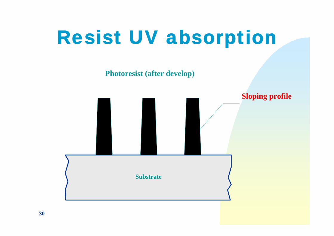
Resist UV absorptionPhotoresist (after develop)
Substrate
Sloping profile
31
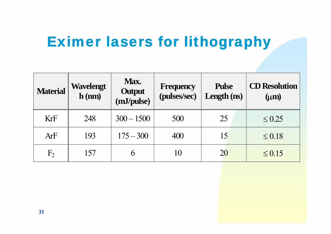
Eximer lasers for lithography
Material Wavelength (nm)
Max.Output
(mJ/pulse)
Frequency(pulses/sec)
PulseLength (ns)
CD Resolution(µm)
KrF 248 300 – 1500 500 25 ≤ 0.25
ArF 193 175 – 300 400 15 ≤ 0.18
F2 157 6 10 20 ≤ 0.15
32
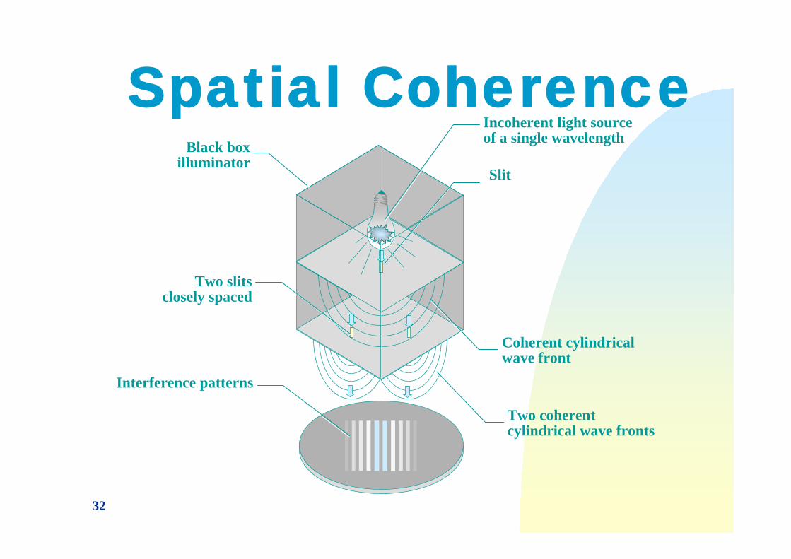
Spatial CoherenceIncoherent light sourceof a single wavelength
Slit
Coherent cylindrical wave front
Two coherent cylindrical wave fronts
Interference patterns
Two slitsclosely spaced
Black box illuminator
33
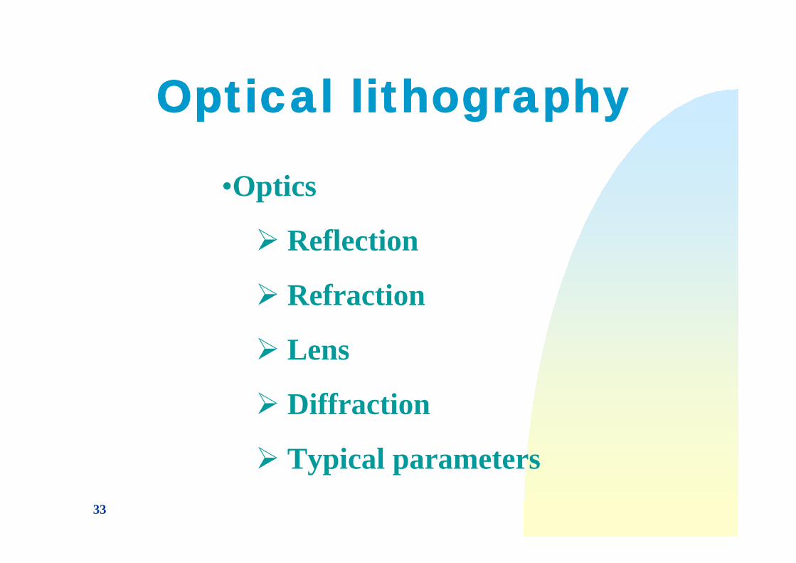
Optical lithography
•Optics
Reflection
Refraction
Lens
Diffraction
Typical parameters
34
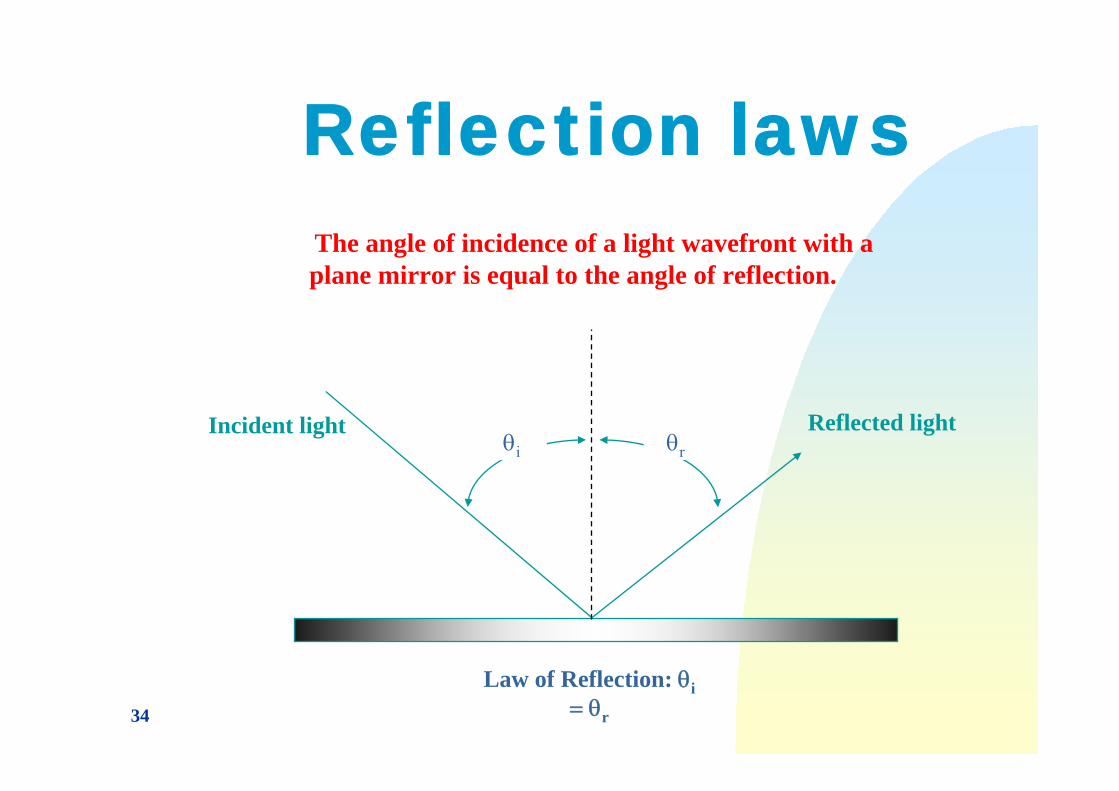
Reflection laws
θi θrIncident light Reflected light
Law of Reflection: θi= θr
The angle of incidence of a light wavefront with a plane mirror is equal to the angle of reflection.
35
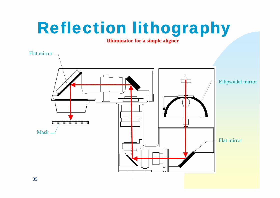
Reflection lithography
Mask
Flat mirror
Ellipsoidal mirror
Flat mirror
Illuminator for a simple aligner
36
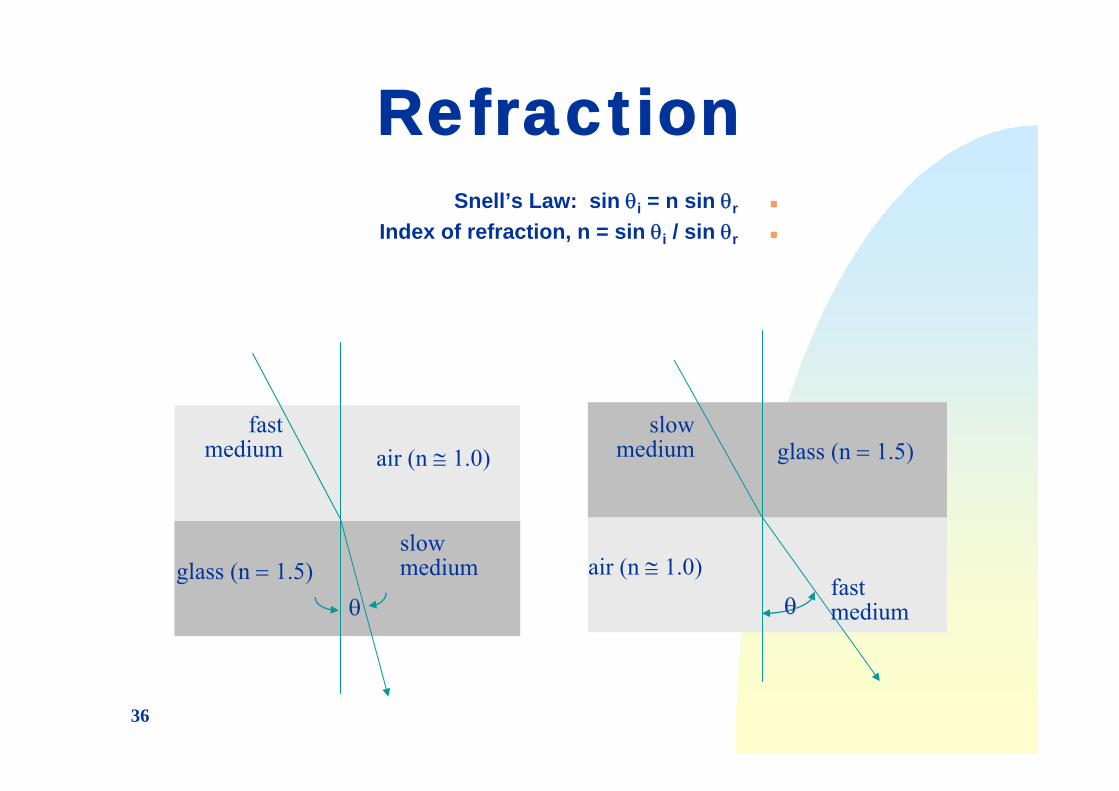
RefractionSnell’s Law: sin θi = n sin θr
Index of refraction, n = sin θi / sin θr
θθ
air (n ≅ 1.0)
glass (n = 1.5)
fast medium
slow medium
θθ
air (n ≅ 1.0)
glass (n = 1.5)
fast medium
slow medium
37
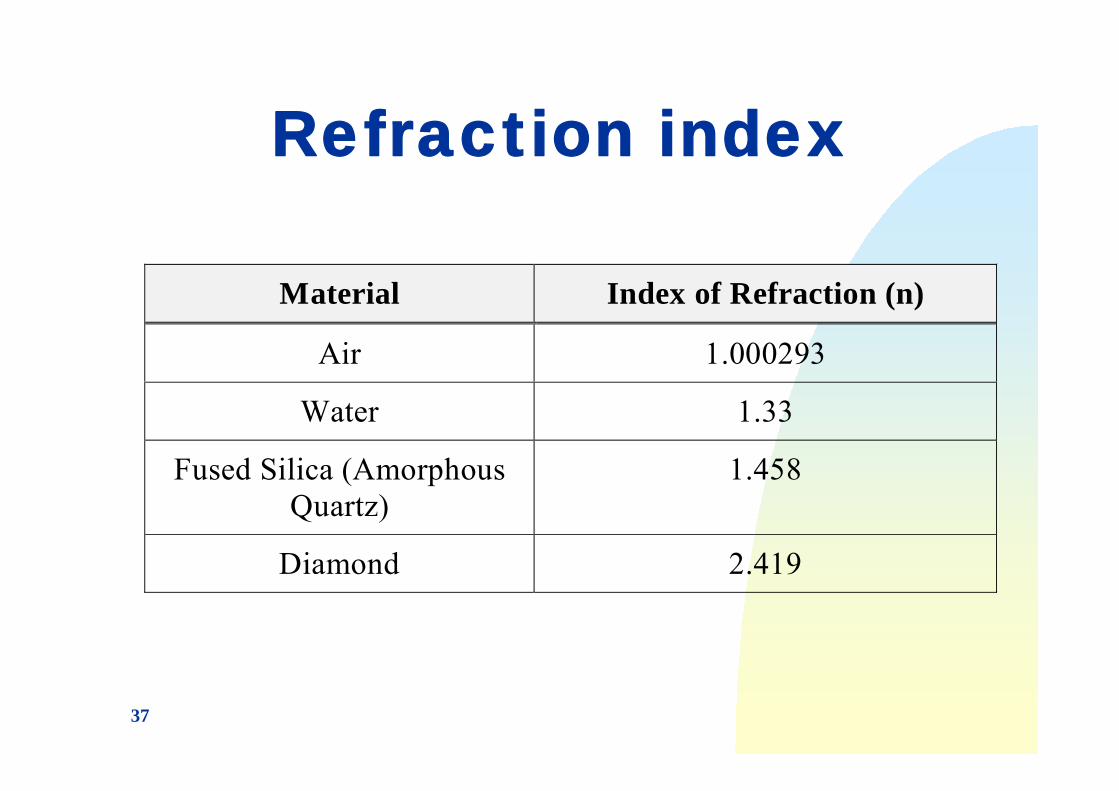
Refraction index
Material Index of Refraction (n)
Air 1.000293
Water 1.33
Fused Silica (AmorphousQuartz)
1.458
Diamond 2.419
38
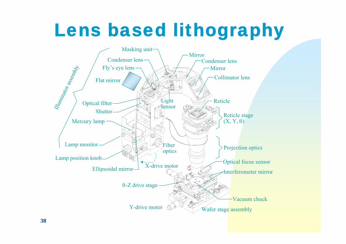
Lens based lithography
Mercury lamp
Lamp position knob
Lamp monitor
Ellipsoidal mirror
Shutter
Fly’s eye lens
Flat mirror
Masking unitMirror
MirrorCollimator lens
Condenser lensCondenser lens
Optical filter
Fiber optics
Reticle
Reticle stage (X, Y, θ)
Projection optics
Optical focus sensor
Interferometer mirrorX-drive motor
Y-drive motor
θ-Z drive stage
Vacuum chuck
Wafer stage assembly
Light sensorIll
umin
ator a
ssem
bly
39
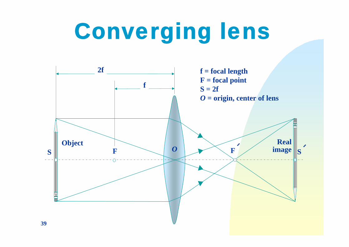
Converging lens
OF F´ S´S
f
2f f = focal lengthF = focal pointS = 2fO = origin, center of lens
Real image
Object

40
Diverging lens
OF F´ S´S
Virtual image
Object
f = focal lengthF = focal pointS = 2fO = origin, center of lens
41
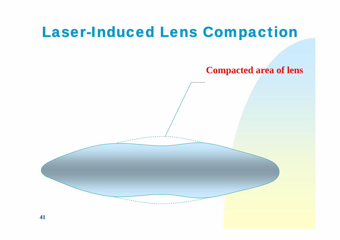
Laser-Induced Lens Compaction
Compacted area of lens
42
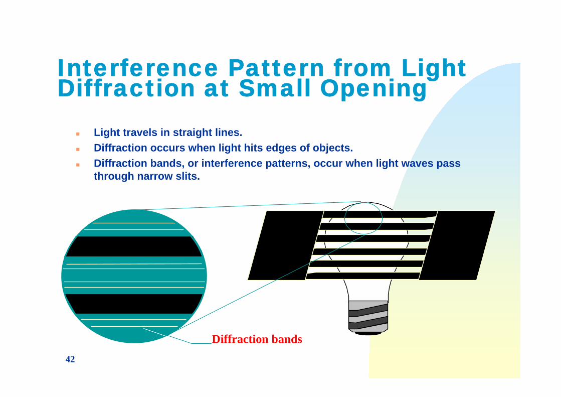
Interference Pattern from Light Diffraction at Small Opening
Light travels in straight lines.Diffraction occurs when light hits edges of objects.Diffraction bands, or interference patterns, occur when light waves pass through narrow slits.
Diffraction bands
43
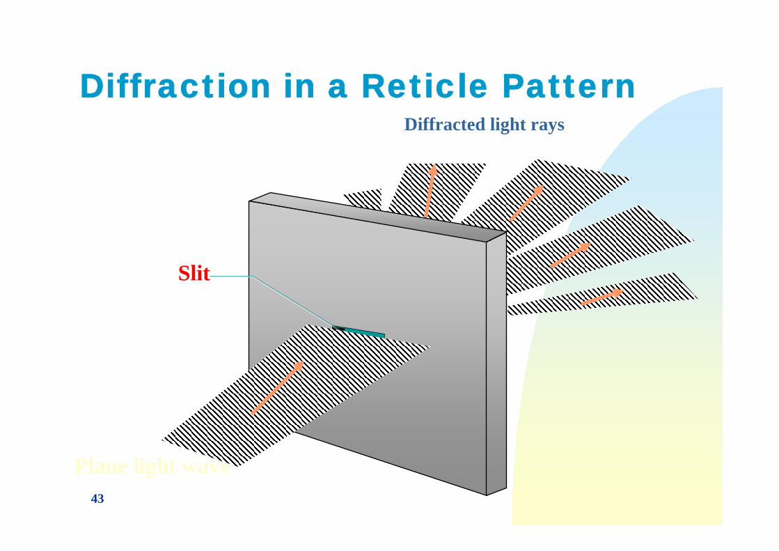
Diffraction in a Reticle Pattern
Slit
Diffracted light rays
Plane light wave
44
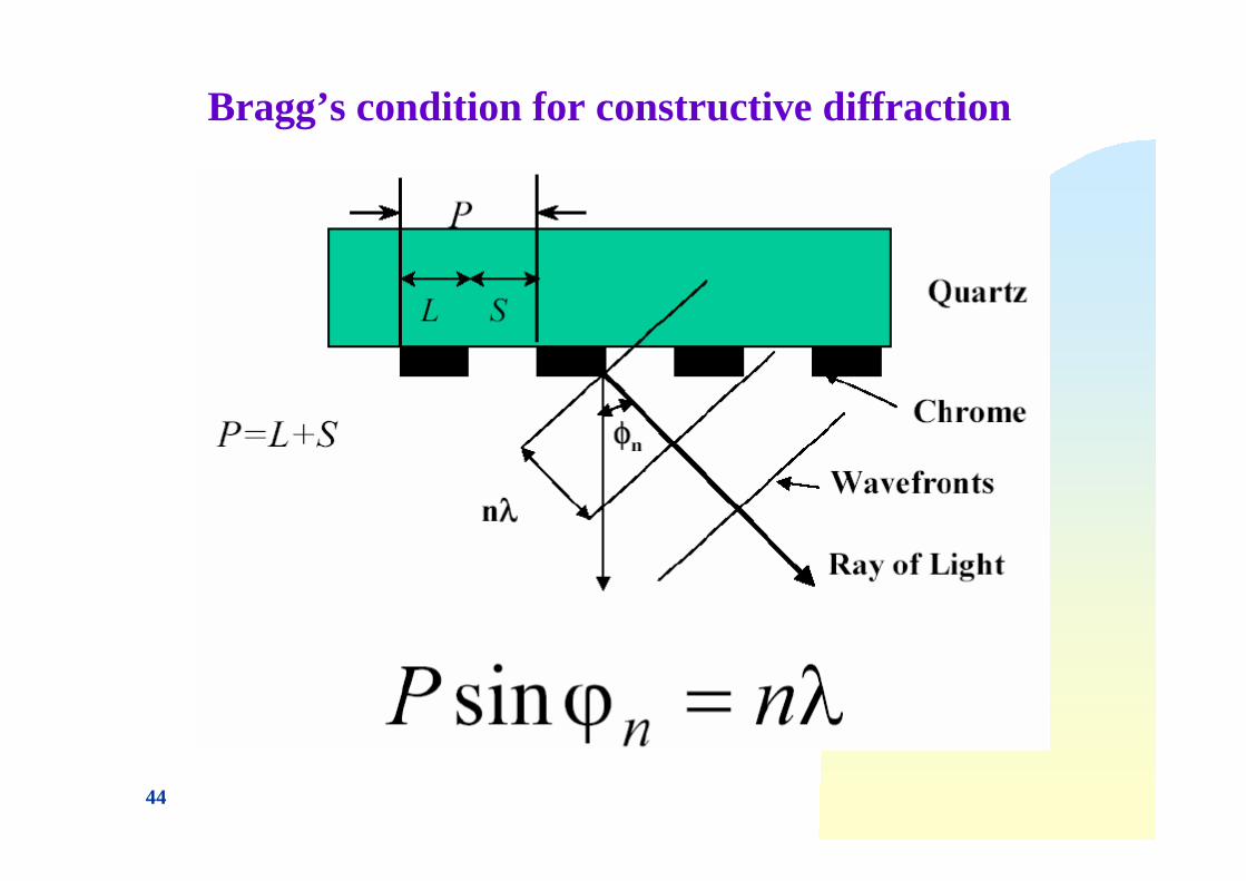
Bragg’s condition for constructive diffraction
45
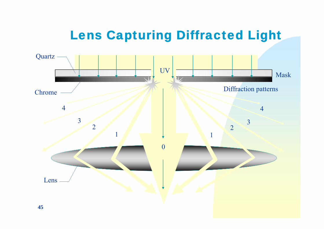
Lens Capturing Diffracted Light
UV
0
12
3
4
12
3
4
Lens
Quartz
Chrome Diffraction patterns
Mask
46
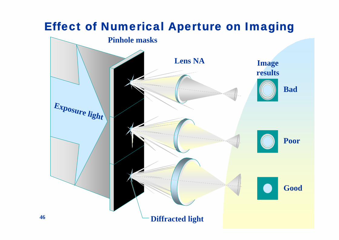
Effect of Numerical Aperture on Imaging
Exposure light
Lens NA
Pinhole masks
Image results
Diffracted light
Good
Bad
Poor

47
Image formation - example
θn
λn=)sin(θp n
Bragg’s law
Quartz plate with chromium pattern with a periodicity (pitch) of p.
Coherent illumination

48
The lens
Focal plane
Lens with diameter D & distance f from the focal plane
Mask
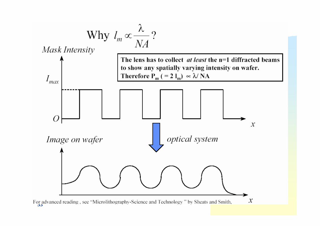
fDnNA
2)sin( ≈= α
49
50
51
52
53
54
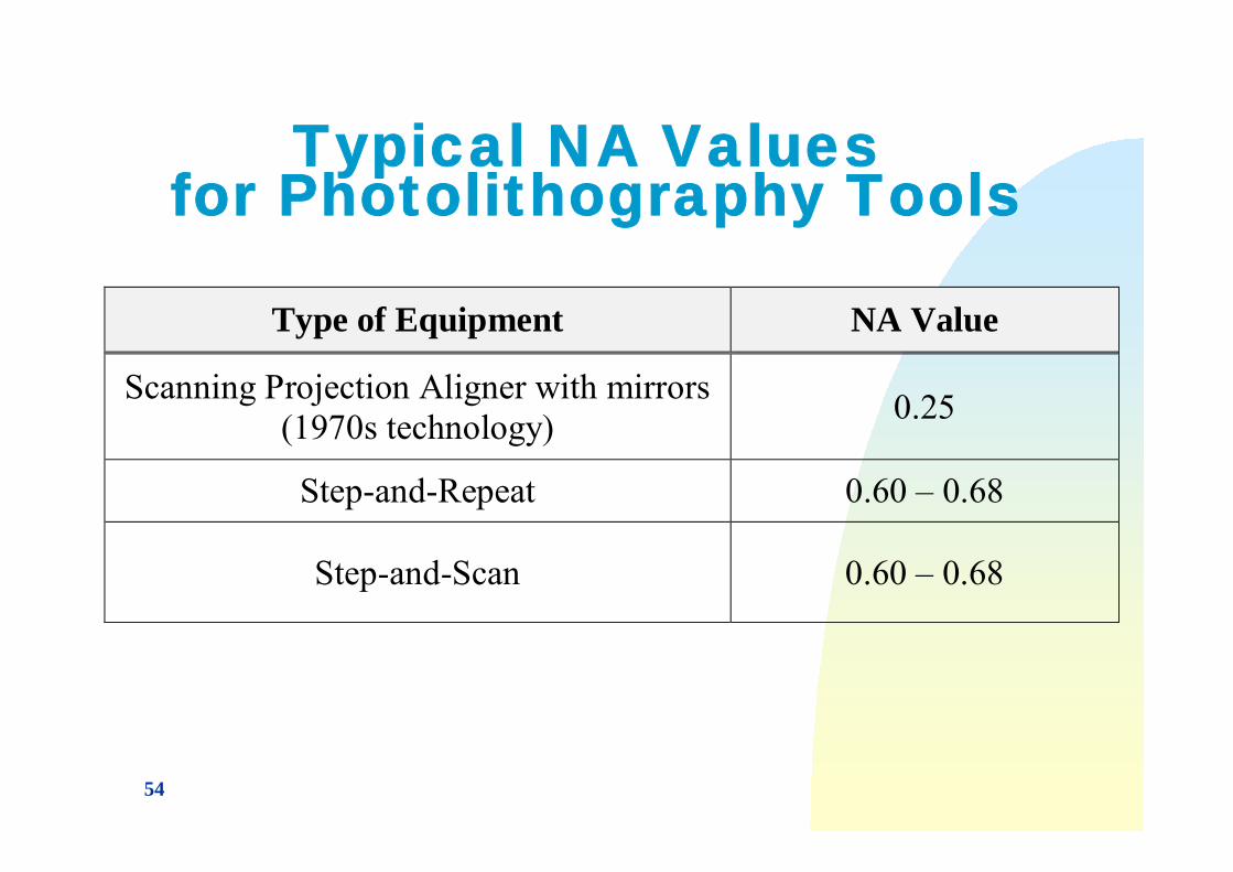
Typical NA Values for Photolithography Tools
Type of Equipment NA Value
Scanning Projection Aligner with mirrors(1970s technology) 0.25
Step-and-Repeat 0.60 – 0.68
Step-and-Scan 0.60 – 0.68
55
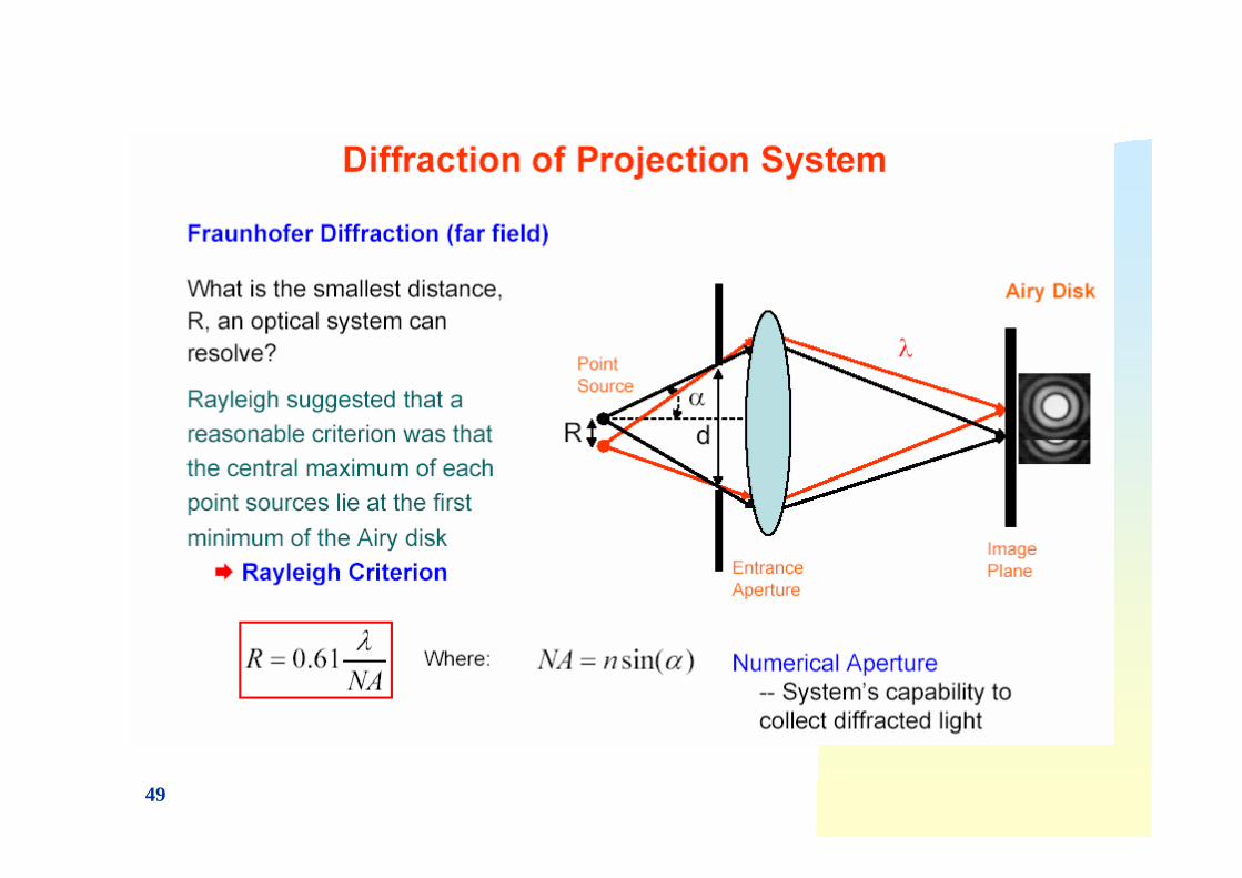
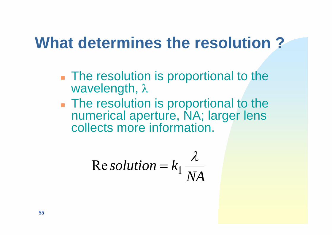
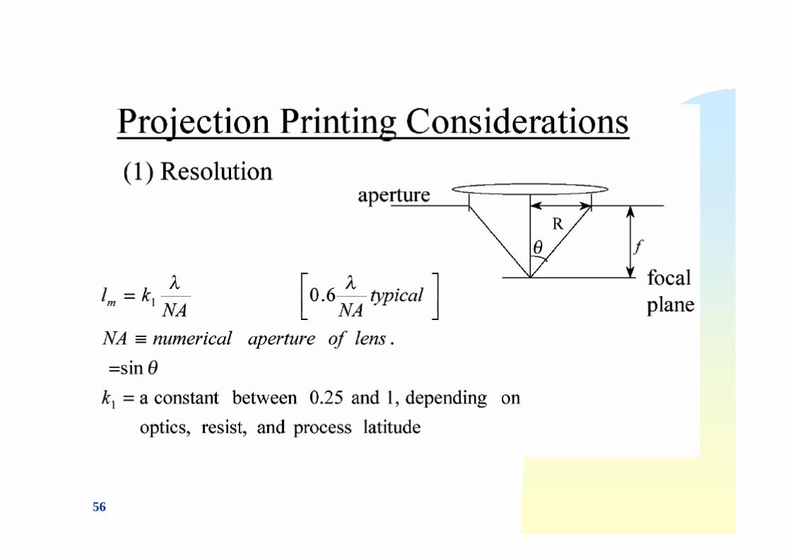
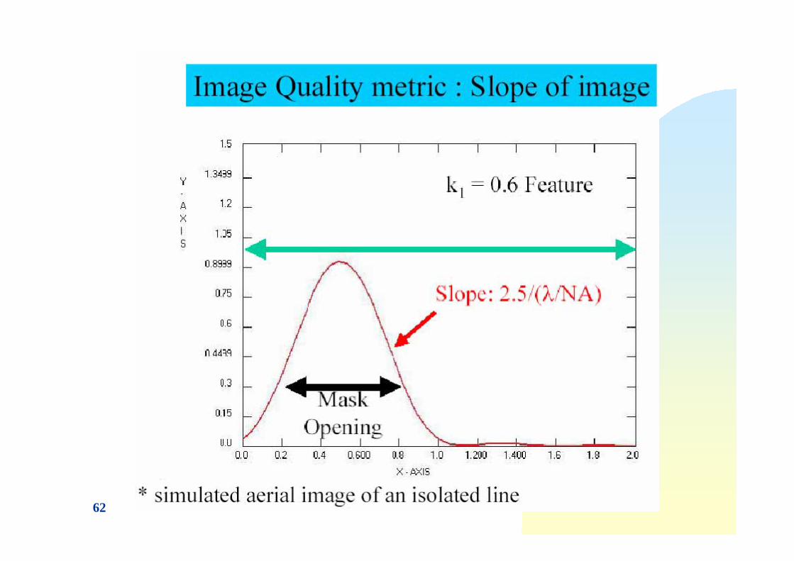
What determines the resolution ?
The resolution is proportional to the wavelength, λThe resolution is proportional to the numerical aperture, NA; larger lens collects more information.
NAksolution λ
1Re =
56
57
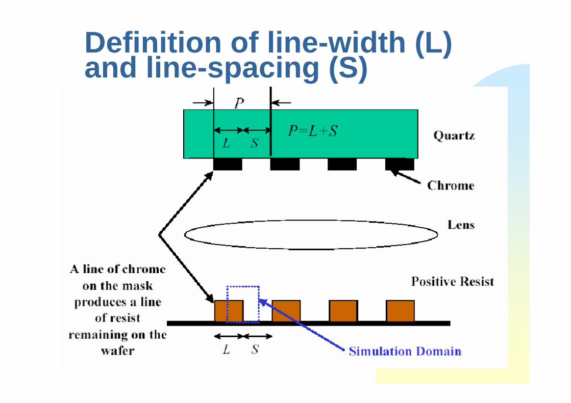
Definition of line-width (L) and line-spacing (S)
58
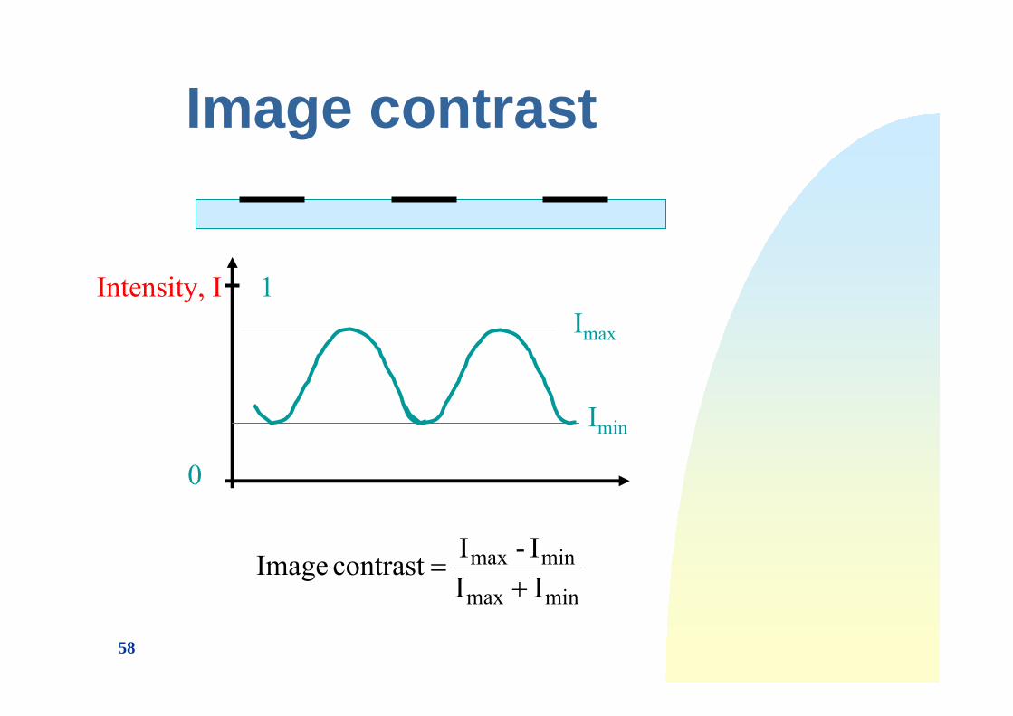
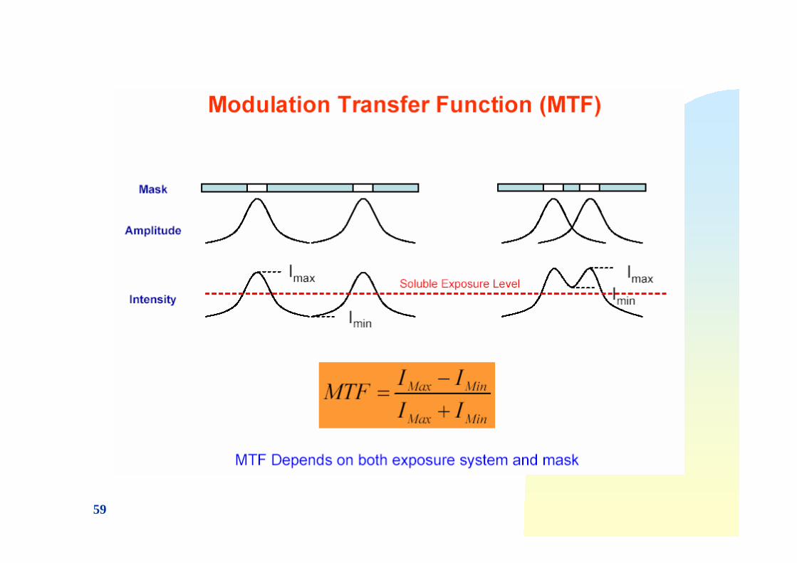
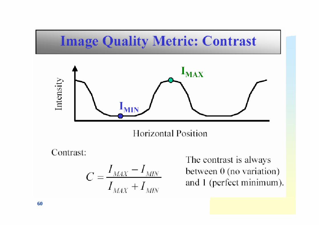
Image contrast
0
1Intensity, IImax
Imin
minmax
minmaxIII-Icontrast Image
+=
59
60
61
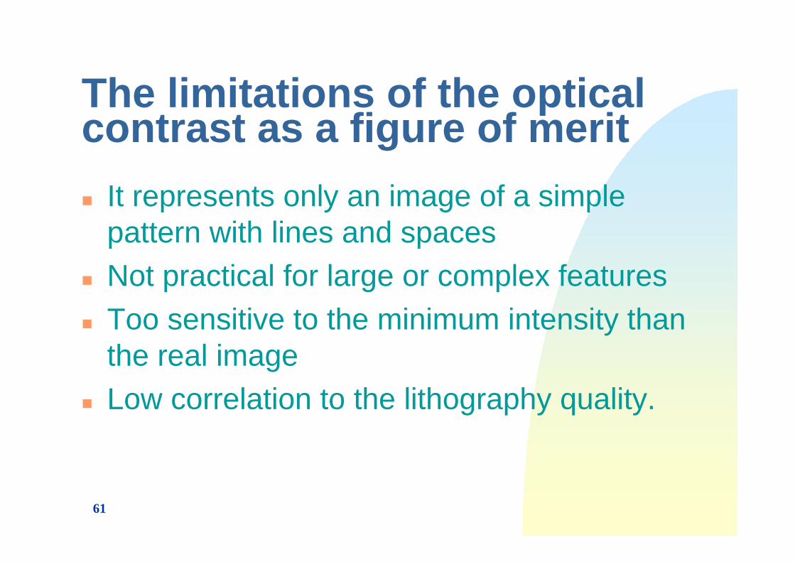
The limitations of the optical contrast as a figure of merit
It represents only an image of a simple pattern with lines and spacesNot practical for large or complex featuresToo sensitive to the minimum intensity than the real imageLow correlation to the lithography quality.
62
63
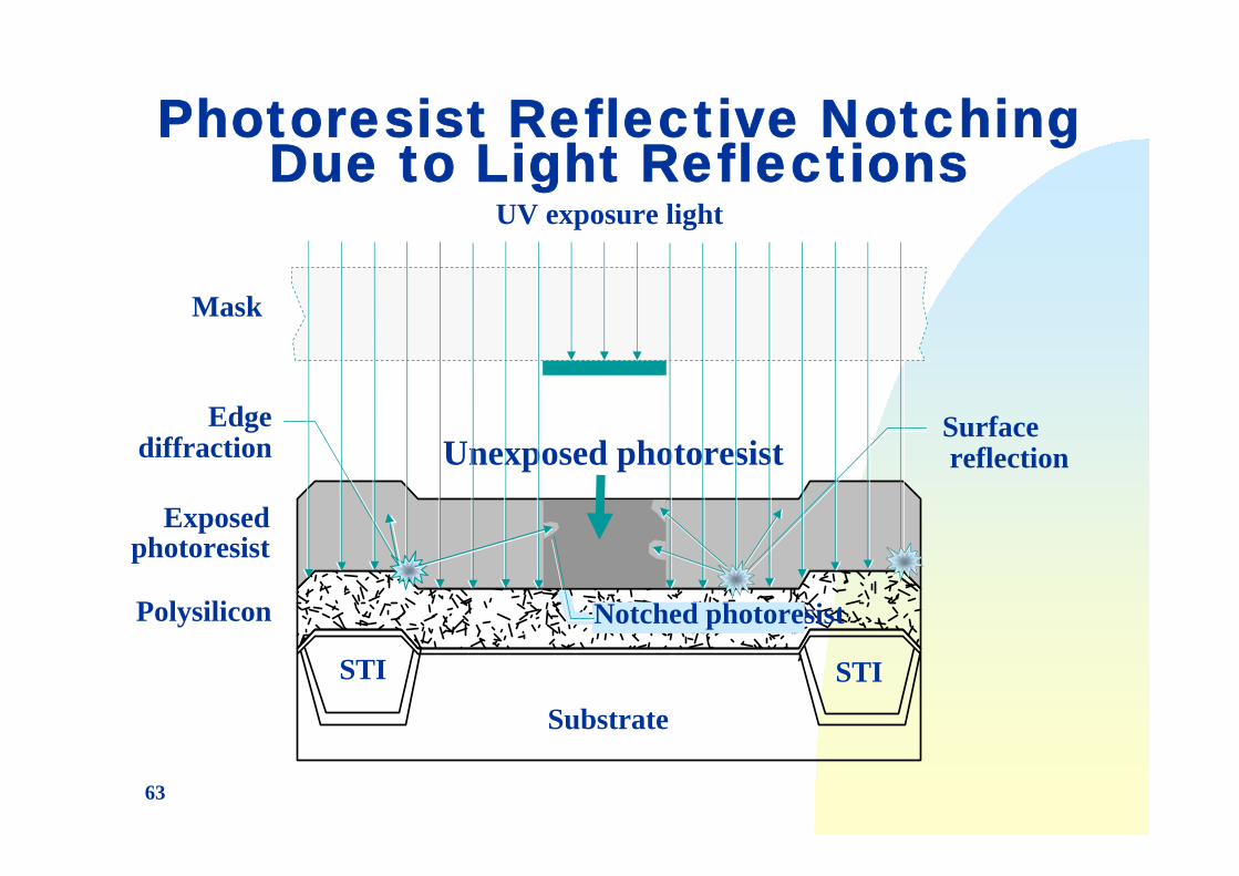
Photoresist Reflective Notching Due to Light Reflections
Exposed photoresist
Surfacereflection
Polysilicon
SubstrateSTISTI
UV exposure light
Mask
Unexposed photoresist
Notched photoresist
Edgediffraction

64
Incident and Reflected Light Wave Interference in Photoresist
Standing waves cause non-uniform exposure along the
thickness of the photoresist film.
Incident waveReflected wave
PhotoresistFilm
Substrate
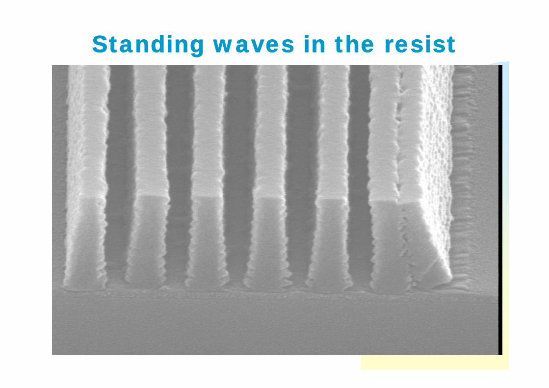
65
Standing waves in the resist
66
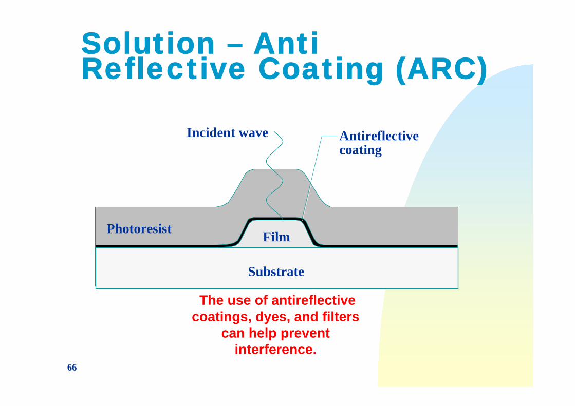
Solution – Anti Reflective Coating (ARC)
The use of antireflective coatings, dyes, and filters
can help prevent interference.
Incident wave Antireflective coating
Photoresist Film
Substrate
67
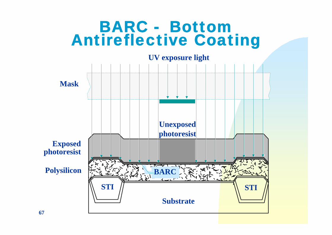
BARC - Bottom Antireflective Coating
BARCPolysilicon
Substrate
STISTI
UV exposure light
Mask
Exposed photoresist
Unexposed photoresist
68
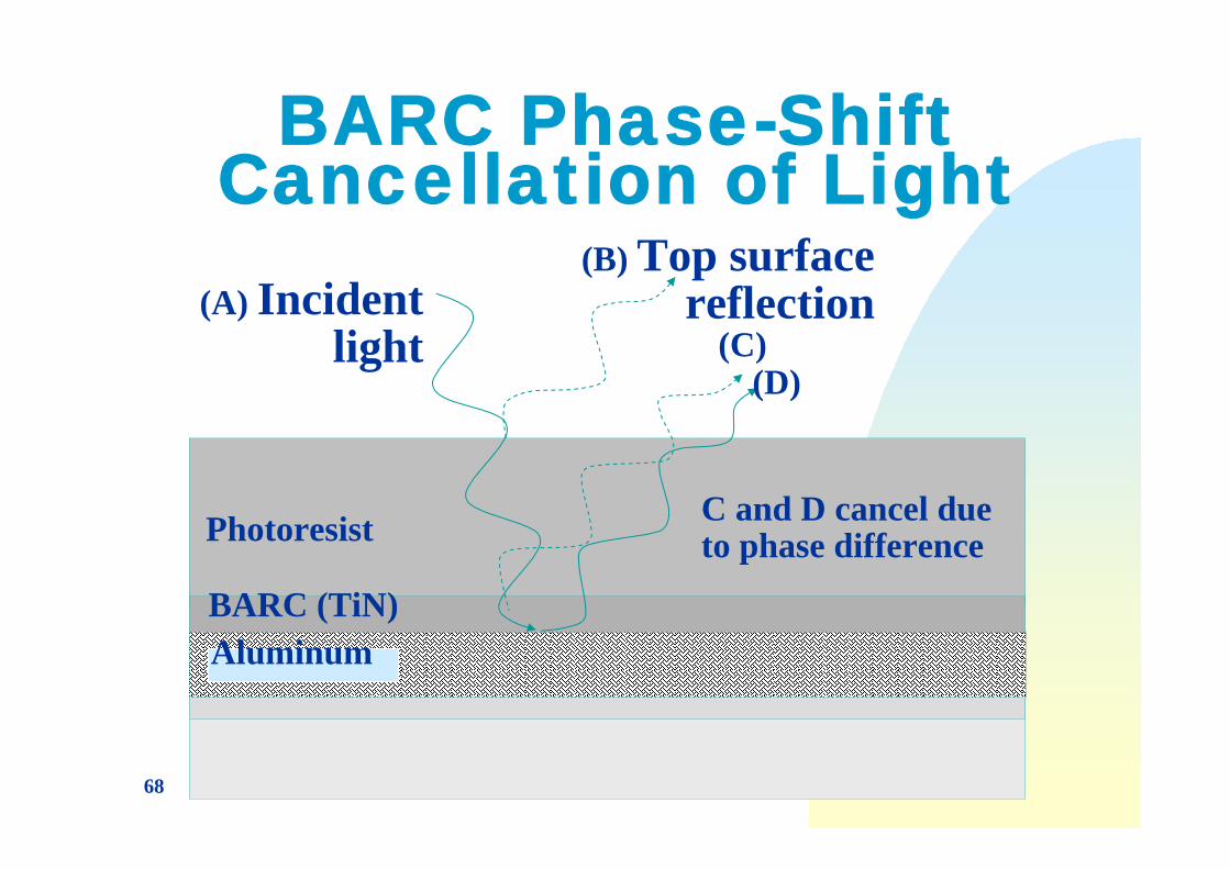
BARC Phase-Shift Cancellation of Light
(A) Incident light
Photoresist
BARC (TiN)Aluminum
C and D cancel due to phase difference
(B) Top surface reflection
(C)(D)
69
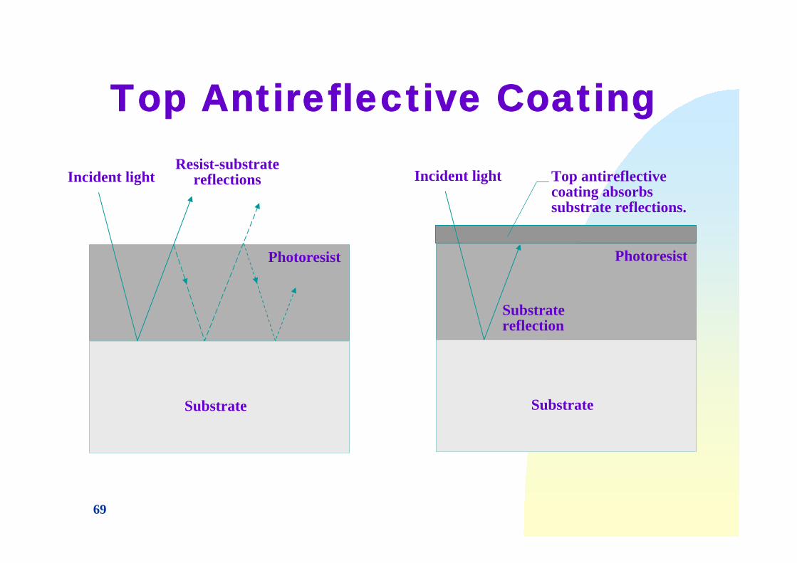
Top Antireflective Coating
Incident light
Photoresist
Resist-substrate reflections
Substrate
Incident light
Photoresist
Substrate reflection
Substrate
Top antireflective coating absorbs substrate reflections.
70
Optical Lithography
ResolutionCalculating ResolutionDepth of FocusResolution Versus Depth of Focus
Surface Planarity
71
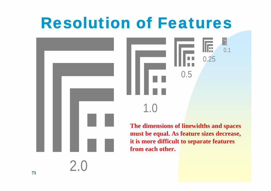
Resolution of Features
2.0
1.0
0.5
0.10.25
The dimensions of linewidths and spaces must be equal. As feature sizes decrease, it is more difficult to separate features from each other.
72
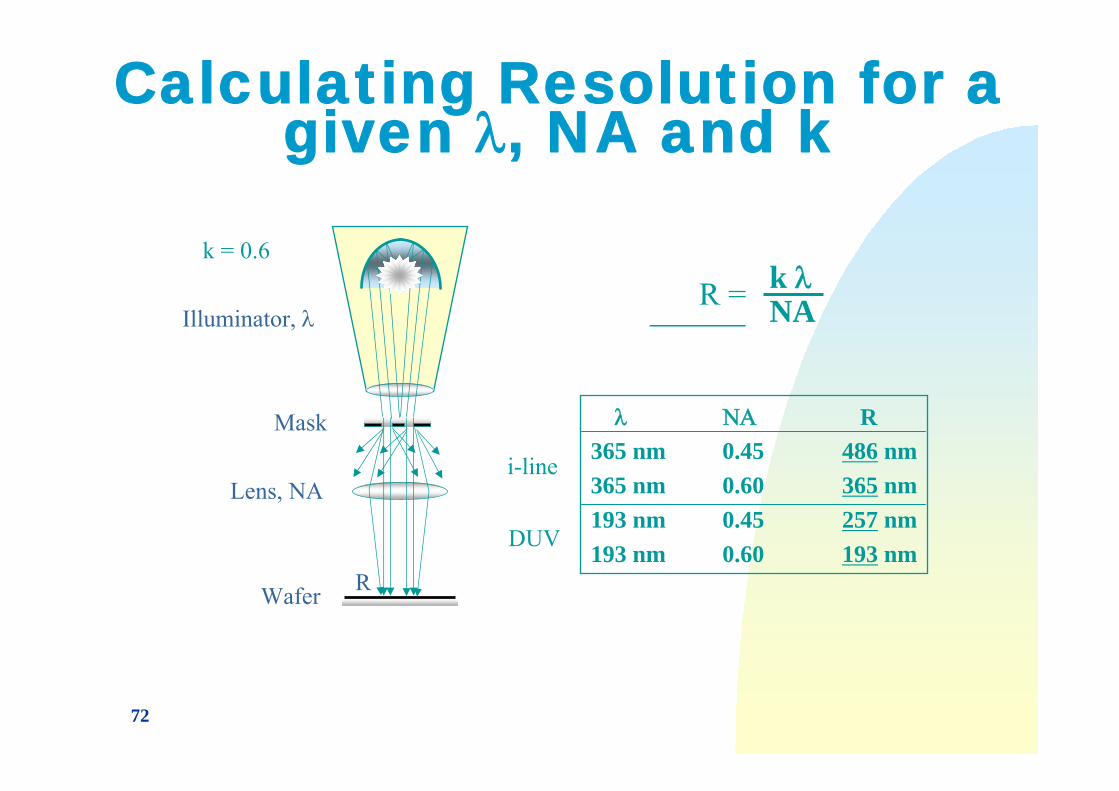
Calculating Resolution for a given λ, NA and k
Lens, NA
Wafer
Mask
Illuminator, λ
R
k = 0.6
λ ΝΑ R365 nm 0.45 486 nm365 nm 0.60 365 nm193 nm 0.45 257 nm193 nm 0.60 193 nm
i-line
DUV
k λNAR =
73
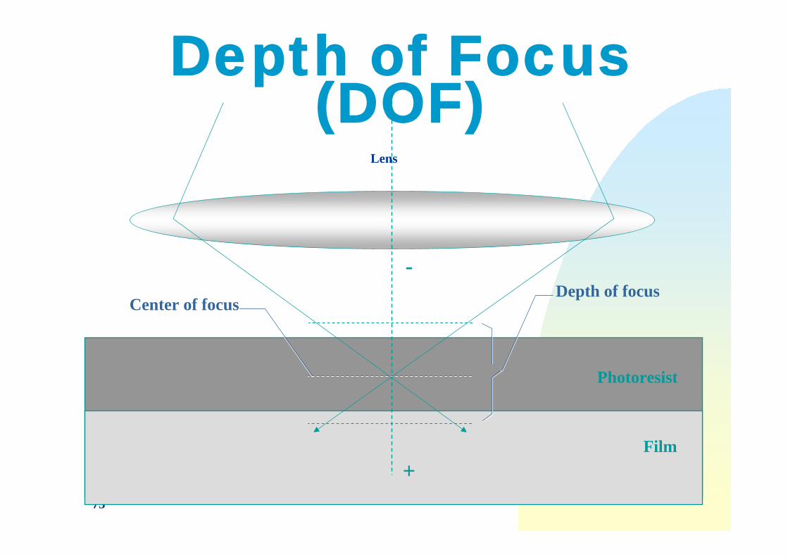
Depth of Focus (DOF)
+
-
Photoresist
Film
Depth of focusCenter of focusCenter of focus
Lens

74
75
76
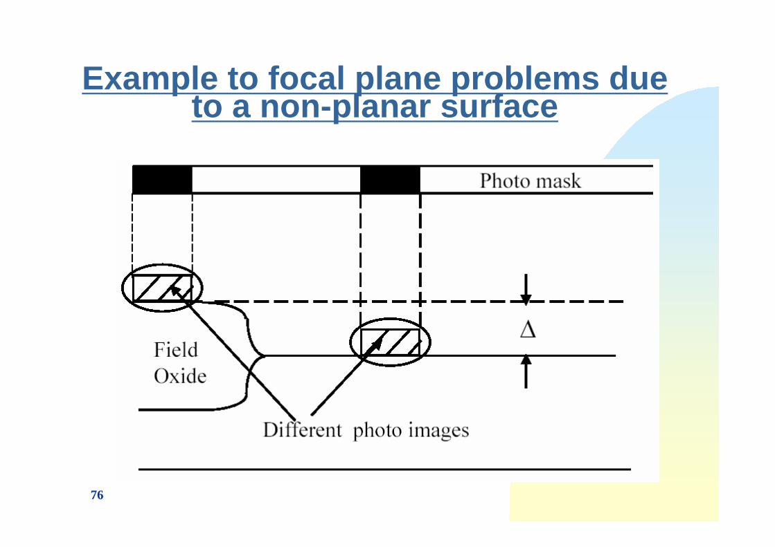
Example to focal plane problems due to a non-planar surface
77
78
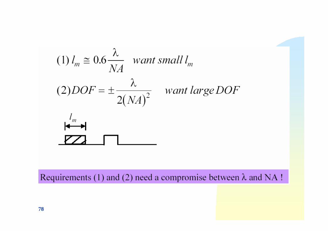
79
80
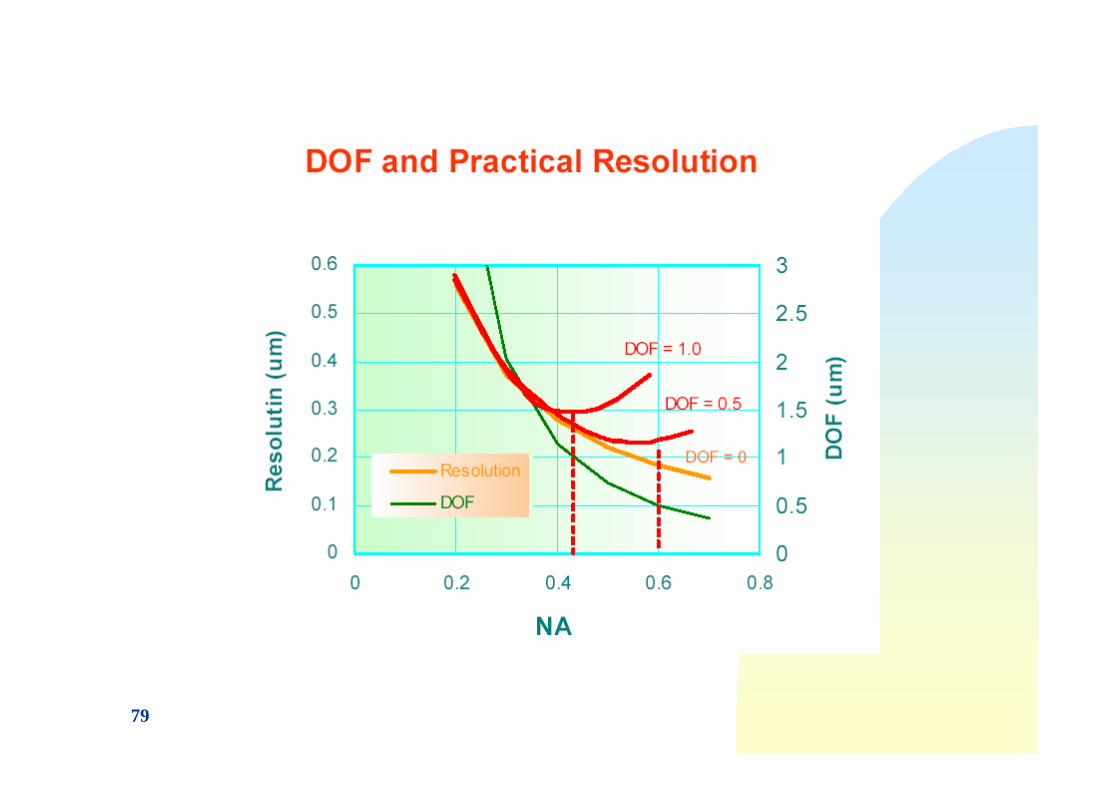
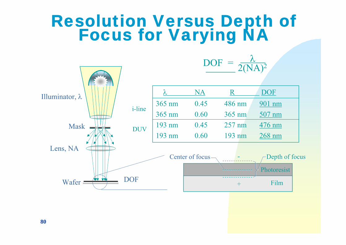
Resolution Versus Depth ofFocus for Varying NA
λ 2(NA)2DOF =
Photoresist
Film
Depth of focusDepth of focusCenter of focus
++
--Lens, NA
Wafer
Mask
Illuminator, λ
DOF
λ ΝΑ R DOF365 nm 0.45 486 nm 901 nm365 nm 0.60 365 nm 507 nm193 nm 0.45 257 nm 476 nm193 nm 0.60 193 nm 268 nm
i-line
DUV
81
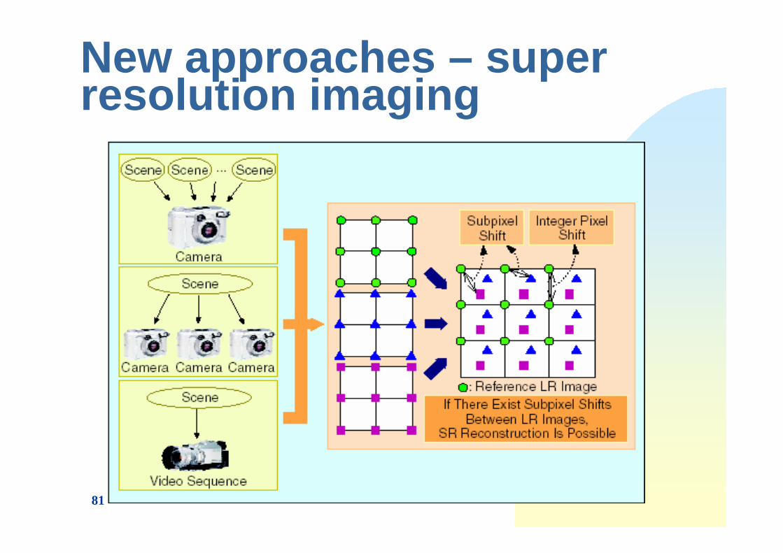
New approaches – super resolution imaging