Embed Size (px)
Citation preview
February 25, 2008
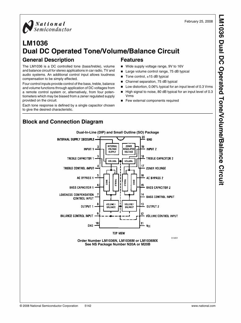
LM1036Dual DC Operated Tone/Volume/Balance CircuitGeneral DescriptionThe LM1036 is a DC controlled tone (bass/treble), volumeand balance circuit for stereo applications in car radio, TV andaudio systems. An additional control input allows loudnesscompensation to be simply effected.
Four control inputs provide control of the bass, treble, balanceand volume functions through application of DC voltages froma remote control system or, alternatively, from four poten-tiometers which may be biased from a zener regulated supplyprovided on the circuit.
Each tone response is defined by a single capacitor chosento give the desired characteristic.
Features■ Wide supply voltage range, 9V to 16V
■ Large volume control range, 75 dB typical
■ Tone control, ±15 dB typical
■ Channel separation, 75 dB typical
■ Low distortion, 0.06% typical for an input level of 0.3 Vrms
■ High signal to noise, 80 dB typical for an input level of 0.3Vrms
■ Few external components required
Block and Connection Diagram
Dual-In-Line (DIP) and Small Outline (SO) Package
514201
Order Number LM1036N, LM1036M or LM1036MXSee NS Package Number N20A or M20B
© 2008 National Semiconductor Corporation 5142 www.national.com
LM
1036 D
ual D
C O
pera
ted
To
ne/V
olu
me/B
ala
nce C
ircu
it

Absolute Maximum Ratings (Note 1)
If Military/Aerospace specified devices are required,please contact the National Semiconductor Sales Office/Distributors for availability and specifications.
Supply Voltage 16V
Control Pin Voltage (Pins 4, 7, 9, 12, 14) VCC
Operating Temperature Range 0°C to +70°C
Storage Temperature Range −65°C to +150°C
Power Dissipation 1W
Lead Temp. (Soldering, 10 seconds) 260°C
Note 1: “Absolute Maximum Ratings” indicate limits beyond which damageto the device may occur. Operating Ratings indicate conditions for which thedevice is functional, but do not guarantee specific performance limits.
Electrical CharacteristicsVCC=12V, TA=25°C (unless otherwise stated)
Parameter Conditions Min Typ Max Units
Supply Voltage Range Pin 11 9 16 V
Supply Current 35 45 mA
Zener Regulated Output Pin 17
Voltage 5.4 V
Current 5 mA
Maximum Output Voltage Pins 8, 13; f=1 kHz
VCC=9V, Maximum Gain 0.8 Vrms
VCC=12V 0.8 1.0 Vrms
Maximum Input Voltage Pins 2, 19; f=1 kHz, VCC 2V 1.3 1.6 Vrms
Gain=−10 dB
Input Resistance Pins 2, 19; f=1 kHz 20 30 kΩOutput Resistance Pins 8, 13; f=1 kHz 20 ΩMaximum Gain V(Pin 12)=V(Pin 17); f=1 kHz −2 0 2 dB
Volume Control Range f=1 kHz 70 75 dB
Gain Tracking f=1 kHz
Channel 1–Channel 2 0 dB through −40 dB 1 3 dB
−40 dB through −60 dB 2 dB
Balance Control Range Pins 8, 13; f=1 kHz 1 dB
−26 −20 dB
Bass Control Range f=40 Hz, Cb=0.39 μF
(Note 3) V(Pin 14)=V(Pin 17) 12 15 18 dB
V(Pin 14)=0V −12 −15 −18 dB
Treble Control Range f= 16 kHz, Ct,=0.01 μF
(Note 3) V(Pin 4)=V(Pin 17) 12 15 18 dB
V(Pin 4)=0V −12 −15 −18 dB
Total Harmonic Distortion f=1 kHz, VIN=0.3 Vrms
Gain=0 dB 0.06 0.3 %
Gain=−30 dB 0.03 %
Channel Separation f=1 kHz, Maximum Gain 60 75 dB
Signal/Noise Ratio Unweighted 100 Hz–20 kHz 80 dB
Maximum Gain, 0 dB=0.3 Vrms
CCIR/ARM (Note 4)
Gain=0 dB, VIN=0.3 Vrms 75 79 dB
Gain=−20 dB, VIN=1.0 Vrms 72 dB
Output Noise Voltage at CCIR/ARM (Note 4) 10 16 μV
Minimum Gain
Supply Ripple Rejection 200 mVrms, 1 kHz Ripple 35 50 dB
Control Input Currents Pins 4, 7, 9, 12, 14 (V=0V) −0.6 −2.5 μA
Frequency Response −1 dB (Flat Response 250 kHz
20 Hz–16 kHz)
www.national.com 2
LM
1036

Note 2: The maximum permissible input level is dependent on tone and volume settings. See Application Notes.
Note 3: The tone control range is defined by capacitors Cb and Ct. See Application Notes.
Note 4: Gaussian noise, measured over a period of 50 ms per channel, with a CCIR filter referenced to 2 kHz and an average-responding meter.
Typical Performance Characteristics
Volume ControlCharacteristics
514220
Balance ControlCharacteristic
514221
Tone Control Characteristic
514222
Tone Characteristic (Gainvs Frequency)
514223
Tone Characteristic (Gainvs Frequency)
514224
Loudness CompensatedVolume Characteristic
514225
3 www.national.com
LM
1036

Input Signal Handling vsSupply Voltage
514226
THD vs Gain
514227
Channel Separation vsFrequency
514228
Loudness ControlCharacteristic
514229
Output Noise Voltagevs Gain
514230
THD vs Input Voltage
514231
www.national.com 4
LM
1036

Application Notes
TONE RESPONSE
The maximum boost and cut can be optimized for individualapplications by selection of the appropriate values of Ct (tre-ble) and Cb (bass).
The tone responses are defined by the relationships:
Where ab=at=0 for maximum bass and treble boost respec-tively and ab=at=1 for maximum cut.
For the values of Cb and Ct of 0.39 μF and 0.01 μF as shownin the Application Circuit, 15 dB of boost or cut is obtained at40 Hz and 16 kHz.
ZENER VOLTAGE
A zener voltage (pin 17=5.4V) is provided which may be usedto bias the control potentiometers. Setting a DC level of onehalf of the zener voltage on the control inputs, pins 4, 9, and14, results in the balanced gain and flat response condition.Typical spread on the zener voltage is ±100 mV and this mustbe taken into account if control signals are used which are notreferenced to the zener voltage. If this is the case, then theywill need to be derived with similar accuracy.
LOUDNESS COMPENSATION
A simple loudness compensation may be effected by applyinga DC control voltage to pin 7. This operates on the tone controlstages to produce an additional boost limited by the maximumboost defined by Cb and Ct. There is no loudness compen-sation when pin 7 is connected to pin 17. Pin 7 can beconnected to pin 12 to give the loudness compensated vol-ume characteristic as illustrated without the addition of furtherexternal components. (Tone settings are for flat response,Cb and Ct as given in Application Circuit.) Modification to theloudness characteristic is possible by changing the capacitorsCb and Ct for a different basic response or, by a resistor net-work between pins 7 and 12 for a different threshold andslope.
SIGNAL HANDLING
The volume control function of the LM1036 is carried out intwo stages, controlled by the DC voltage on pin 12, to improvesignal handling capability and provide a reduction of outputnoise level at reduced gain. The first stage is before the tonecontrol processing and provides an initial 15 dB of gain re-duction, so ensuring that the tone sections are not overdrivenby large input levels when operating with a low volume setting.Any combination of tone and volume settings may be usedprovided the output level does not exceed 1 Vrms, VCC=12V(0.8 Vrms, VCC=9V). At reduced gain (<−6 dB)the input stagewill overload if the input level exceeds 1.6 Vrms, VCC=12V(1.1 Vrms, VCC=9V). As there is volume control on the inputstages, the inputs may be operated with a lower overloadmargin than would otherwise be acceptable, allowing a pos-sible improvement in signal to noise ratio.
Application Circuit
514203
5 www.national.com
LM
1036

Applications Information
OBTAINING MODIFIED RESPONSE CURVES
The LM1036 is a dual DC controlled bass, treble, balance andvolume integrated circuit ideal for stereo audio systems.
In the various applications where the LM1036 can be used,there may be requirements for responses different to those ofthe standard application circuit given in the data sheet. Thisapplication section details some of the simple variations pos-sible on the standard responses, to assist the choice of opti-mum characteristics for particular applications.
TONE CONTROLS
Summarizing the relationship given in the data sheet, basi-cally for an increase in the treble control range Ct must beincreased, and for increased bass range Cb must be reduced.
Figure 1 shows the typical tone response obtained in thestandard application circuit. (Ct=0.01 μF, Cb=0.39 μF). Re-sponse curves are given for various amounts of boost and cut.
514204
FIGURE 1. Tone Characteristic (Gain vs Frequency)
Figure 2 and Figure 3 show the effect of changing the re-sponse defining capacitors Ct and Cb to 2Ct, Cb/2 and 4Ct,Cb/4 respectively, giving increased tone control ranges. Thevalues of the bypass capacitors may become significant andaffect the lower frequencies in the bass response curves.
514205
FIGURE 2. Tone Characteristic (Gain vs Frequency)
514206
FIGURE 3. Tone Characteristic (Gain vs Frequency)
Figure 4 shows the effect of changing Ct and Cb in the oppo-site direction to Ct/2, 2Cb respectively giving reduced controlranges. The various results corresponding to the different Ctand Cb values may be mixed if it is required to give a particularemphasis to, for example, the bass control. The particularcase with Cb/2, Ct is illustrated in Figure 5.
Restriction of Tone Control Action at High or LowFrequencies
It may be desired in some applications to level off the toneresponses above or below certain frequencies for example toreduce high frequence noise.
This may be achieved for the treble response by including aresistor in series with Ct. The treble boost and cut will be 3 dBless than the standard circuit when R=XC.
A similar effect may be obtained for the bass response byreducing the value of the AC bypass capacitors on pins 5(channel 1) and 16 (channel 2). The internal resistance atthese pins is 1.3 kΩ and the bass boost/cut will be approxi-mately 3 dB less with XC at this value. An example of suchmodified response curves is shown in Figure 6. The inputcoupling capacitors may also modify the low frequency re-sponse.
It will be seen from Figure 2 and Figure 3 that modifying Ctand Cb for greater control range also has the effect of flatten-ing the tone control extremes and this may be utilized, with orwithout additional modification as outlined above, for the mostsuitable tone control range and response shape.
Other Advantages of DC Controls
The DC controls make the addition of other features easy toarrange. For example, the negative-going peaks of the outputamplifiers may be detected below a certain level, and used tobias back the bass control from a high boost condition, toprevent overloading the speaker with low frequency compo-nents.
LOUDNESS CONTROL
The loudness control is achieved through control of the tonesections by the voltage applied to pin 7; therefore, the toneand loudness functions are not independent. There is nor-mally 1 dB more bass than treble boost (40 Hz–16 kHz) withloudness control in the standard circuit. If a greater differenceis desired, it is necessary to introduce an offset by means ofCt or Cb or by changing the nominal control voltage ranges.
Figure 7 shows the typical loudness curves obtained in thestandard application circuit at various volume levels (Cb=0.39μF).
www.national.com 6
LM
1036

514207
FIGURE 4. Tone Characteristic (Gain vs Frequency)
514208
FIGURE 5. Tone Characteristic (Gain vs Frequency)
514209
FIGURE 6. Tone Characteristic (Gain vs Frequency)
514210
FIGURE 7. Loudness Compensated VolumeCharacteristic
Figure 8 and Figure 9 illustrate the loudness characteristicsobtained with Cb changed to Cb/2 and Cb/4 respectively, Ctbeing kept at the nominal 0.01 μF. These values naturallymodify the bass tone response as in Figure 2 and Figure 3.
With pins 7 (loudness) and 12 (volume) directly connected,loudness control starts at typically −8 dB volume, with mostof the control action complete by −30 dB.
Figure 10 and Figure 11 show the effect of resistively offset-ting the voltage applied to pin 7 towards the control referencevoltage (pin 17). Because the control inputs are highimpedance, this is easily done and high value resistors maybe used for minimal additional loading. It is possible to reducethe rate of onset of control to extend the active range to−50 dB volume control and below.
The control on pin 7 may also be divided down towardsground bringing the control action on earlier. This is illustratedin Figure 12, With a suitable level shifting network betweenpins 12 and 7, the onset of loudness control and its rate ofchange may be readily modified.
514211
FIGURE 8. Loudness Compensated VolumeCharacteristic
514212
FIGURE 9. Loudness Compensated VolumeCharacteristic
7 www.national.com
LM
1036

514213
FIGURE 10. Loudness Compensated VolumeCharacteristic
514214
FIGURE 11. Loudness Compensated VolumeCharacteristic
514215
FIGURE 12. Loudness Compensated VolumeCharacteristic
When adjusted for maximum boost in the usual applicationcircuit, the LM1036 cannot give additional boost from theloudness control with reducing gain. If it is required, someadditional boost can be obtained by restricting the tone controlrange and modifying Ct, Cb, to compensate. A circuit illustrat-ing this for the case of bass boost is shown in Figure 13. Theresulting responses are given in Figure 14 showing the con-tinuing loudness control action possible with bass boost pre-viously applied.
USE OF THE LM1036 ABOVE AUDIO FREQUENCIES
The LM1036 has a basic response typically 1 dB down at 250kHz (tone controls flat) and therefore by scaling Cb and Ct, itis possible to arrange for operation over a wide frequencyrange for possible use in wide band equalization applications.As an example Figure 15 shows the responses obtained cen-tered on 10 kHz with Cb=0.039 μF and Ct=0.001 μF.
www.national.com 8
LM
1036

514216
FIGURE 13. Modified Application Circuit for Additional Bass Boost with Loudness Control
514217
FIGURE 14. Loudness Compensated Volume Characteristic
514218
FIGURE 15. Tone Characteristic (Gain vs Frequency)
9 www.national.com
LM
1036

Simplified Schematic Diagram
(One Channel)
514219
*Connections reversed
www.national.com 10
LM
1036

Physical Dimensions inches (millimeters) unless otherwise noted
Molded Dual-In-Line Package (N)Order Number LM1036N
NS Package Number N20A
Small Outline (SO) PackageOrder Number LM1036M or LM1036MX
NS Package Number M20B
11 www.national.com
LM
1036

NotesL
M1036 D
ual D
C O
pera
ted
To
ne/V
olu
me/B
ala
nce C
ircu
it
For more National Semiconductor product information and proven design tools, visit the following Web sites at:
Products Design Support
Amplifiers www.national.com/amplifiers WEBENCH www.national.com/webench
Audio www.national.com/audio Analog University www.national.com/AU
Clock Conditioners www.national.com/timing App Notes www.national.com/appnotes
Data Converters www.national.com/adc Distributors www.national.com/contacts
Displays www.national.com/displays Green Compliance www.national.com/quality/green
Ethernet www.national.com/ethernet Packaging www.national.com/packaging
Interface www.national.com/interface Quality and Reliability www.national.com/quality
LVDS www.national.com/lvds Reference Designs www.national.com/refdesigns
Power Management www.national.com/power Feedback www.national.com/feedback
Switching Regulators www.national.com/switchers
LDOs www.national.com/ldo
LED Lighting www.national.com/led
PowerWise www.national.com/powerwise
Serial Digital Interface (SDI) www.national.com/sdi
Temperature Sensors www.national.com/tempsensors
Wireless (PLL/VCO) www.national.com/wireless
THE CONTENTS OF THIS DOCUMENT ARE PROVIDED IN CONNECTION WITH NATIONAL SEMICONDUCTOR CORPORATION(“NATIONAL”) PRODUCTS. NATIONAL MAKES NO REPRESENTATIONS OR WARRANTIES WITH RESPECT TO THE ACCURACYOR COMPLETENESS OF THE CONTENTS OF THIS PUBLICATION AND RESERVES THE RIGHT TO MAKE CHANGES TOSPECIFICATIONS AND PRODUCT DESCRIPTIONS AT ANY TIME WITHOUT NOTICE. NO LICENSE, WHETHER EXPRESS,IMPLIED, ARISING BY ESTOPPEL OR OTHERWISE, TO ANY INTELLECTUAL PROPERTY RIGHTS IS GRANTED BY THISDOCUMENT.
TESTING AND OTHER QUALITY CONTROLS ARE USED TO THE EXTENT NATIONAL DEEMS NECESSARY TO SUPPORTNATIONAL’S PRODUCT WARRANTY. EXCEPT WHERE MANDATED BY GOVERNMENT REQUIREMENTS, TESTING OF ALLPARAMETERS OF EACH PRODUCT IS NOT NECESSARILY PERFORMED. NATIONAL ASSUMES NO LIABILITY FORAPPLICATIONS ASSISTANCE OR BUYER PRODUCT DESIGN. BUYERS ARE RESPONSIBLE FOR THEIR PRODUCTS ANDAPPLICATIONS USING NATIONAL COMPONENTS. PRIOR TO USING OR DISTRIBUTING ANY PRODUCTS THAT INCLUDENATIONAL COMPONENTS, BUYERS SHOULD PROVIDE ADEQUATE DESIGN, TESTING AND OPERATING SAFEGUARDS.
EXCEPT AS PROVIDED IN NATIONAL’S TERMS AND CONDITIONS OF SALE FOR SUCH PRODUCTS, NATIONAL ASSUMES NOLIABILITY WHATSOEVER, AND NATIONAL DISCLAIMS ANY EXPRESS OR IMPLIED WARRANTY RELATING TO THE SALEAND/OR USE OF NATIONAL PRODUCTS INCLUDING LIABILITY OR WARRANTIES RELATING TO FITNESS FOR A PARTICULARPURPOSE, MERCHANTABILITY, OR INFRINGEMENT OF ANY PATENT, COPYRIGHT OR OTHER INTELLECTUAL PROPERTYRIGHT.
LIFE SUPPORT POLICY
NATIONAL’S PRODUCTS ARE NOT AUTHORIZED FOR USE AS CRITICAL COMPONENTS IN LIFE SUPPORT DEVICES ORSYSTEMS WITHOUT THE EXPRESS PRIOR WRITTEN APPROVAL OF THE CHIEF EXECUTIVE OFFICER AND GENERALCOUNSEL OF NATIONAL SEMICONDUCTOR CORPORATION. As used herein:
Life support devices or systems are devices which (a) are intended for surgical implant into the body, or (b) support or sustain life andwhose failure to perform when properly used in accordance with instructions for use provided in the labeling can be reasonably expectedto result in a significant injury to the user. A critical component is any component in a life support device or system whose failure to performcan be reasonably expected to cause the failure of the life support device or system or to affect its safety or effectiveness.
National Semiconductor and the National Semiconductor logo are registered trademarks of National Semiconductor Corporation. All otherbrand or product names may be trademarks or registered trademarks of their respective holders.
Copyright© 2008 National Semiconductor Corporation
For the most current product information visit us at www.national.com
National SemiconductorAmericas TechnicalSupport CenterEmail:[email protected]: 1-800-272-9959
National Semiconductor EuropeTechnical Support CenterEmail: [email protected] Tel: +49 (0) 180 5010 771English Tel: +44 (0) 870 850 4288
National Semiconductor AsiaPacific Technical Support CenterEmail: [email protected]
National Semiconductor JapanTechnical Support CenterEmail: [email protected]
www.national.com


![VYSOKÉ UČENÍ TECHNICKÉ V BRNĚTabulka 1 Základní parametry obvodu LM1036 [2] 4.1.2. Popis zapojení Zapojení korekčního předzesilovače je na Obr. 5. Integrovaný obvod LM](https://img.pdfslide.net/doc/110x75/60fdd3743731812c5f7f6748/vysok-uoeen-technick-v-brn-tabulka-1-zkladn-parametry-obvodu-lm1036.jpg)