Embed Size (px)
Citation preview
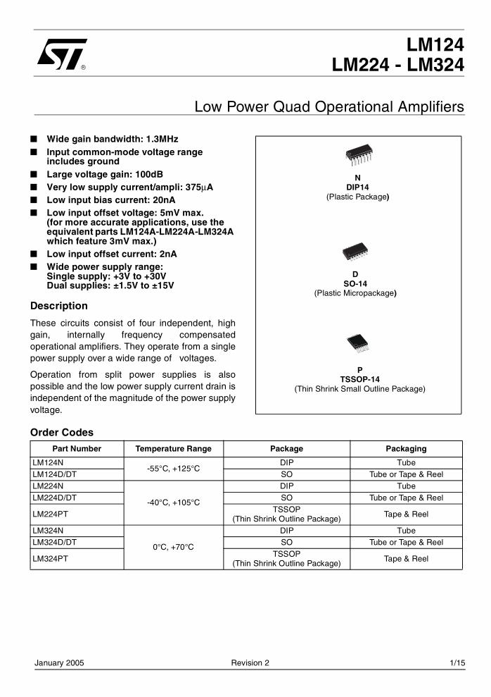
LM124LM224 - LM324
Low Power Quad Operational Amplifiers
Wide gain bandwidth: 1.3MHz Input common-mode voltage range
includes ground Large voltage gain: 100dB Very low supply current/ampli: 375µA Low input bias current: 20nA Low input offset voltage: 5mV max.
(for more accurate applications, use the equivalent parts LM124A-LM224A-LM324A which feature 3mV max.)
Low input offset current: 2nA Wide power supply range:
Single supply: +3V to +30VDual supplies: ±1.5V to ±15V
Description
These circuits consist of four independent, highgain, internally frequency compensatedoperational amplifiers. They operate from a singlepower supply over a wide range of voltages.
Operation from split power supplies is alsopossible and the low power supply current drain isindependent of the magnitude of the power supplyvoltage.
Order Codes
NDIP14
(Plastic Package)
DSO-14
(Plastic Micropackage)
PTSSOP-14
(Thin Shrink Small Outline Package)
Part Number Temperature Range Package Packaging
LM124N-55°C, +125°C
DIP TubeLM124D/DT SO Tube or Tape & ReelLM224N
-40°C, +105°C
DIP TubeLM224D/DT SO Tube or Tape & Reel
LM224PTTSSOP
(Thin Shrink Outline Package)Tape & Reel
LM324N
0°C, +70°C
DIP TubeLM324D/DT SO Tube or Tape & Reel
LM324PTTSSOP
(Thin Shrink Outline Package)Tape & Reel
January 2005 Revision 2 1/15
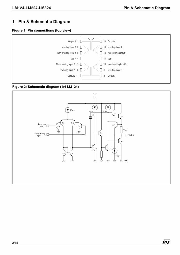
LM124-LM224-LM324 Pin & Schematic Diagram
1 Pin & Schematic Diagram
Figure 1: Pin connections (top view)
Figure 2: Schematic diagram (1/4 LM124)
Inverting Input 2
Non-inverting Input 2
Non-inverting Input 1
CCV -CCV
1
2
3
4
8
5
6
7
9
10
11
12
13
14
+
Output 3
Output 4
Non-inverting Input 4
Inverting Input 4
Non-inverting Input 3
Inverting Input 3
-
+
-
+
-
+
-
+
Output 1
Inverting Input 1
Output 2
2/15

Absolute Maximum Ratings LM124-LM224-LM324
2 Absolute Maximum Ratings
Table 1: Key parameters and their absolute maximum ratings
Symbol Parameter LM124 LM224 LM324 Unit
VCC Supply voltage ±16 or 32 VVi Input Voltage -0.3 to Vcc + 0.3 V
Vid Differential Input Voltage 1
1) Either or both input voltages must not exceed the magnitude of VCC+ or VCC
-.
-0.3 to Vcc + 0.3 V
PtotPower Dissipation N Suffix
D Suffix500 500
400500400
mWmW
Output Short-circuit Duration 2
2) Short-circuits from the output to VCC can cause excessive heating if VCC > 15V. The maximum output current is approximately 40mAindependent of the magnitude of VCC. Destructive dissipation can result from simultaneous short-circuit on all amplifiers.
Infinite
Iin Input Current 3
3) This input current only exists when the voltage at any of the input leads is driven negative. It is due to the collector-base junction of theinput PNP transistor becoming forward biased and thereby acting as input diodes clamps. In addition to this diode action, there is alsoNPN parasitic action on the IC chip. this transistor action can cause the output voltages of the op-amps to go to the VCC voltage level (orto ground for a large overdrive) for the time duration than an input is driven negative.This is not destructive and normal output will set up again for input voltage higher than -0.3V.
50 50 50 mA
Toper Operating Free-air Temperature Range -55 to +125 -40 to +105 0 to +70 °C
Tstg Storage Temperature Range -65 to +150 °C
Rthja
Thermal Resistance Junction to AmbientSO14TSSOP14DIP14
10310066
°C/W
3/15
LM124-LM224-LM324 Electrical Characteristics
3 Electrical Characteristics
Table 2: VCC+ = +5V, VCC
-= Ground, Vo = 1.4V, Tamb = +25°C (unless otherwise specified)
Symbol Parameter Min. Typ. Max. Unit
Vio
Input Offset Voltage - note 1 Tamb = +25°C LM324Tmin ≤ Tamb ≤ Tmax LM324
2 5779
mV
Iio
Input Offset Current Tamb = +25°CTmin ≤ Tamb ≤ Tmax
2 30100
nA
IibInput Bias Current - note 2
Tamb = +25°CTmin ≤ Tamb ≤ Tmax
20 150300
nA
Avd
Large Signal Voltage GainVCC
+ = +15V, RL = 2kΩ, Vo = 1.4V to 11.4VTamb = +25°CTmin ≤ Tamb ≤ Tmax
5025
100V/mV
SVR
Supply Voltage Rejection Ratio (Rs ≤ 10kΩ)
VCC+ = 5V to 30V
Tamb = +25°CTmin ≤ Tamb ≤ Tmax
6565
110dB
ICC
Supply Current, all Amp, no load Tamb = +25°C VCC = +5V VCC = +30VTmin ≤ Tamb ≤ Tmax VCC = +5V VCC = +30V
0.71.50.81.5
1.23
1.23
mA
Vicm
Input Common Mode Voltage RangeVCC
= +30V - note 3
Tamb = +25°CTmin ≤ Tamb ≤ Tmax
00
VCC -1.5VCC -2
V
CMRCommon Mode Rejection Ratio (Rs ≤ 10kΩ)
Tamb = +25°CTmin ≤ Tamb ≤ Tmax
7060
80 dB
IsourceOutput Current Source (Vid = +1V)
VCC = +15V, Vo = +2V 20 40 70mA
Isink
Output Sink Current (Vid = -1V)VCC = +15V, Vo = +2VVCC = +15V, Vo = +0.2V
1012
2050
mAµA
VOH
High Level Output VoltageVCC = +30VTamb = +25°C RL = 2kΩTmin ≤ Tamb ≤ TmaxTamb = +25°C RL = 10kΩTmin ≤ Tamb ≤ TmaxVCC = +5V, RL = 2kΩTamb = +25°CTmin ≤ Tamb ≤ Tmax
26262727
3.53
27
28
V
4/15
Electrical Characteristics LM124-LM224-LM324
VOL
Low Level Output Voltage (RL = 10kΩ)Tamb = +25°CTmin ≤ Tamb ≤ Tmax
5 2020
mV
SRSlew Rate
VCC = 15V, Vi = 0.5 to 3V, RL = 2kΩ, CL = 100pF, unity Gain 0.4V/µs
GBPGain Bandwidth Product
VCC = 30V, f =100kHz,Vin = 10mV, RL = 2kΩ, CL = 100pF 1.3MHz
THDTotal Harmonic Distortion
f = 1kHz, Av = 20dB, RL = 2kΩ, Vo = 2Vpp, CL = 100pF, VCC = 30V 0.015%
enEquivalent Input Noise Voltage
f = 1kHz, Rs = 100Ω, VCC = 30V 40
DVio Input Offset Voltage Drift 7 30 µV/°C
DIIio Input Offset Current Drift 10 200 pA/°C
Vo1/Vo2Channel Separation - note 4
1kHz ≤ f ≤ 20kHZ 120dB
1) Vo = 1.4V, Rs = 0Ω, 5V < VCC+ < 30V, 0 < Vic < VCC
+ - 1.5V
2) The direction of the input current is out of the IC. This current is essentially constant, independent of the state of the output so no loadingchange exists on the input lines.
3) The input common-mode voltage of either input signal voltage should not be allowed to go negative by more than 0.3V. The upper endof the common-mode voltage range is VCC
+ - 1.5V, but either or both inputs can go to +32V without damage.
4) Due to the proximity of external components insure that coupling is not originating via stray capacitance between these external parts.This typically can be detected as this type of capacitance increases at higher frequencies.
Table 3: Vcc+ = +15V, Vcc
- = 0V, Tamb = 25°C (unless otherwise specified)
Symbol Conditions Value Unit
Vio 0 mV
Avd RL = 2kΩ 100 V/mV
Icc No load, per amplifier 350 µA
Vicm -15 to +13.5 V
VOH RL = 2kΩ (VCC+=15V) +13.5 V
VOL RL = 10kΩ 5 mV
Ios Vo = +2V, VCC = +15V +40 mA
GBP RL = 2kΩ, CL = 100pF 1.3 MHz
SR RL = 2kΩ, CL = 100pF 0.4 V/µs
Table 2: VCC+ = +5V, VCC
-= Ground, Vo = 1.4V, Tamb = +25°C (unless otherwise specified)
Symbol Parameter Min. Typ. Max. Unit
nV
Hz------------
5/15
LM124-LM224-LM324 Electrical Characteristics
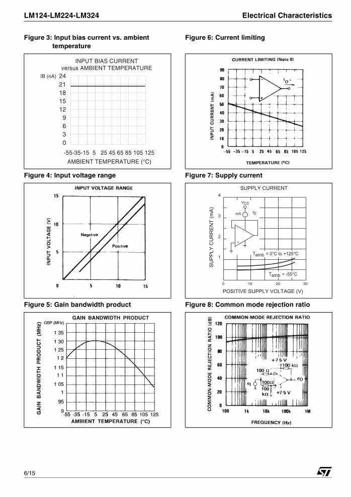
Figure 3: Input bias current vs. ambient temperature
Figure 4: Input voltage range
Figure 5: Gain bandwidth product
-55-35-15 5 25 45 65 85 105 125
AMBIENT TEMPERATURE (°C)
24211815
912
630
INPUT BIAS CURRENTversus AMBIENT TEMPERATURE
IB (nA)
Figure 6: Current limiting
Figure 7: Supply current
Figure 8: Common mode rejection ratio
6/15

Electrical Characteristics LM124-LM224-LM324
Figure 9: Electrical curves
7/15

LM124-LM224-LM324 Electrical Characteristics
Figure 10: Input current
Figure 11: Power supply & common mode rejection ratio
Figure 12: Large signal voltage gain
Figure 13: Voltage gain
8/15
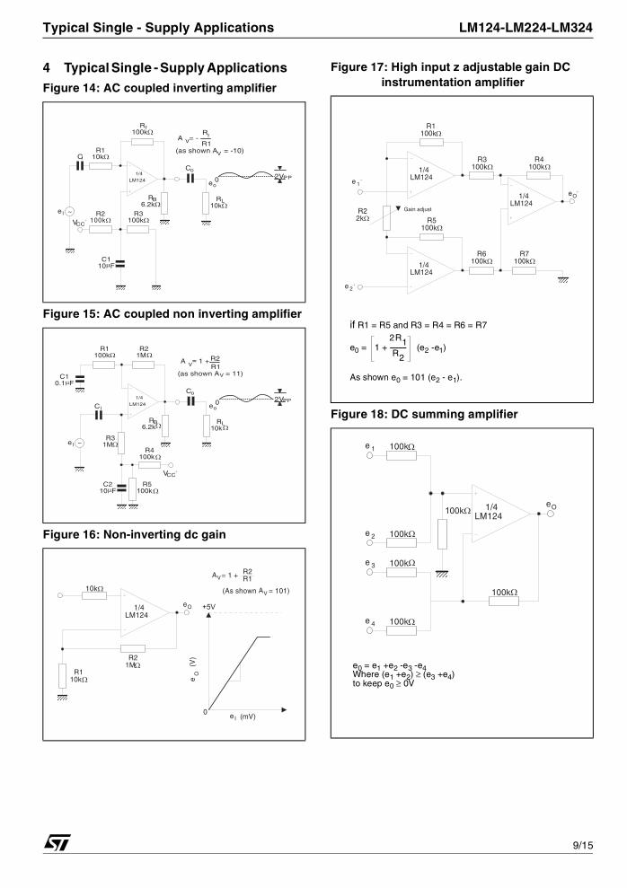
Typical Single - Supply Applications LM124-LM224-LM324
4 Typical Single - Supply Applications
Figure 14: AC coupled inverting amplifier
Figure 15: AC coupled non inverting amplifier
Figure 16: Non-inverting dc gain
Figure 17: High input z adjustable gain DCinstrumentation amplifier
Figure 18: DC summing amplifier
if R1 = R5 and R3 = R4 = R6 = R7
e0 = (e2 -e1)
As shown e0 = 101 (e2 - e1).
12R1R2
-----------+
e0 = e1 +e2 -e3 -e4Where (e1 +e2) ≥ (e3 +e4)to keep e0 ≥ 0V
9/15
LM124-LM224-LM324 Typical Single - Supply Applications
Figure 19: Low drift peak detector
Figure 20: Activer bandpass filter
Fo = 1kHz
Q = 50
Av = 100 (40dB)
Figure 21: High input Z, DC differential amplifier
Figure 22: Using symetrical amplifiers to reduce input current (general concept)
For
(CMRR depends on this resistor ratio match)
R1R2-------
R4R3-------=
e0 (e2 - e1)
As shown e0 = (e2 - e1)
1R4R3-------+⎝ ⎠
⎛ ⎞
10/15

Macromodel LM124-LM224-LM324
11/15
5 Macromodel
Warning: Please consider following remarks before using this macromodel:All models are a trade-off between accuracy and complexity (i.e. simulation time).Macromodels are not a substitute to breadboarding; rather, they confirm the validity of a design approachand help to select surrounding component values.A macromodel emulates the NOMINAL performance of a TYPICAL device within SPECIFIED OPERATINGCONDITIONS (i.e. temperature, supply voltage, etc.). Thus the macromodel is often not as exhaustive asthe datasheet, its goal is to illustrate the main parameters of the product.Data issued from macromodels used outside of its specified conditions (Vcc, Temperature, etc) or evenworse: outside of the device operating conditions (Vcc, Vicm, etc) are not reliable in any way.
** Standard Linear Ics Macromodels, 1993. ** CONNECTIONS :* 1 INVERTING INPUT* 2 NON-INVERTING INPUT* 3 OUTPUT* 4 POSITIVE POWER SUPPLY* 5 NEGATIVE POWER SUPPLY
.SUBCKT LM124 1 3 2 4 5 (analog)*******************************************************.MODEL MDTH D IS=1E-8 KF=3.104131E-15 CJO=10F* INPUT STAGECIP 2 5 1.000000E-12CIN 1 5 1.000000E-12EIP 10 5 2 5 1EIN 16 5 1 5 1RIP 10 11 2.600000E+01RIN 15 16 2.600000E+01RIS 11 15 2.003862E+02DIP 11 12 MDTH 400E-12DIN 15 14 MDTH 400E-12VOFP 12 13 DC 0 VOFN 13 14 DC 0IPOL 13 5 1.000000E-05CPS 11 15 3.783376E-09DINN 17 13 MDTH 400E-12VIN 17 5 0.000000e+00DINR 15 18 MDTH 400E-12VIP 4 18 2.000000E+00FCP 4 5 VOFP 3.400000E+01FCN 5 4 VOFN 3.400000E+01FIBP 2 5 VOFN 2.000000E-03FIBN 5 1 VOFP 2.000000E-03* AMPLIFYING STAGEFIP 5 19 VOFP 3.600000E+02FIN 5 19 VOFN 3.600000E+02RG1 19 5 3.652997E+06RG2 19 4 3.652997E+06CC 19 5 6.000000E-09DOPM 19 22 MDTH 400E-12DONM 21 19 MDTH 400E-12HOPM 22 28 VOUT 7.500000E+03VIPM 28 4 1.500000E+02HONM 21 27 VOUT 7.500000E+03VINM 5 27 1.500000E+02EOUT 26 23 19 5 1VOUT 23 5 0ROUT 26 3 20COUT 3 5 1.000000E-12DOP 19 25 MDTH 400E-12VOP 4 25 2.242230E+00DON 24 19 MDTH 400E-12VON 24 5 7.922301E-01.ENDS
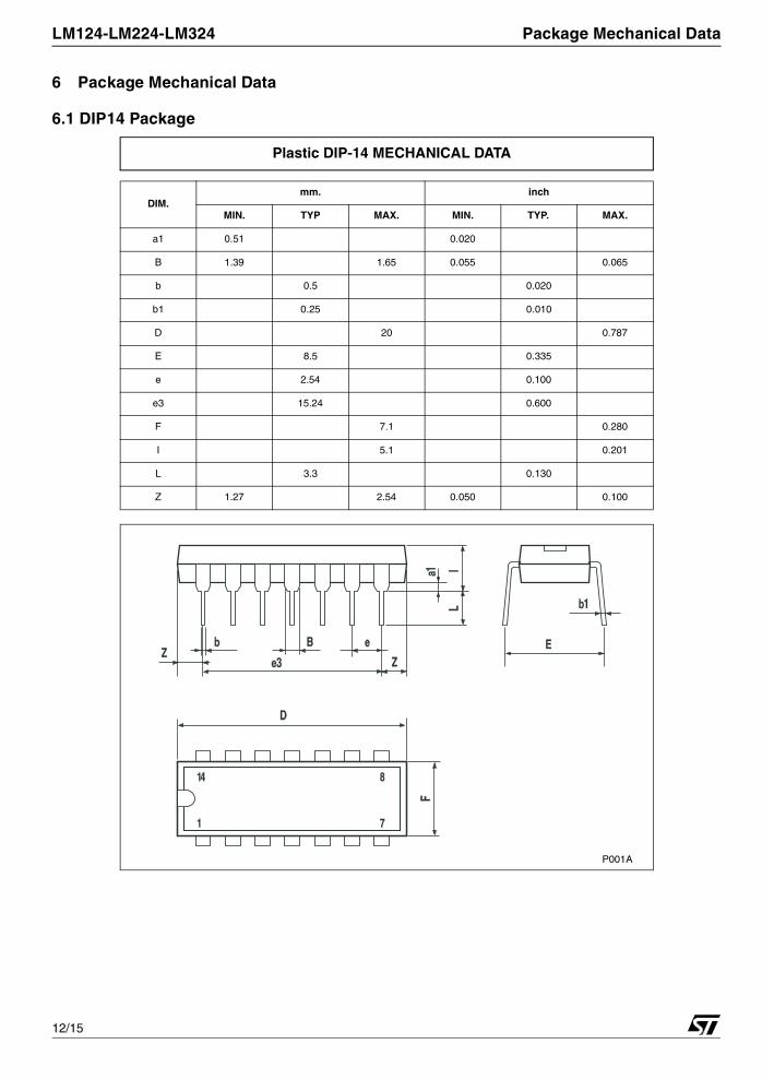
LM124-LM224-LM324 Package Mechanical Data
6 Package Mechanical Data
6.1 DIP14 Package
DIM.mm. inch
MIN. TYP MAX. MIN. TYP. MAX.
a1 0.51 0.020
B 1.39 1.65 0.055 0.065
b 0.5 0.020
b1 0.25 0.010
D 20 0.787
E 8.5 0.335
e 2.54 0.100
e3 15.24 0.600
F 7.1 0.280
I 5.1 0.201
L 3.3 0.130
Z 1.27 2.54 0.050 0.100
Plastic DIP-14 MECHANICAL DATA
P001A
12/15

Package Mechanical Data LM124-LM224-LM324
6.2 SO-14 Package
DIM.mm. inch
MIN. TYP MAX. MIN. TYP. MAX.
A 1.75 0.068
a1 0.1 0.2 0.003 0.007
a2 1.65 0.064
b 0.35 0.46 0.013 0.018
b1 0.19 0.25 0.007 0.010
C 0.5 0.019
c1 45˚ (typ.)
D 8.55 8.75 0.336 0.344
E 5.8 6.2 0.228 0.244
e 1.27 0.050
e3 7.62 0.300
F 3.8 4.0 0.149 0.157
G 4.6 5.3 0.181 0.208
L 0.5 1.27 0.019 0.050
M 0.68 0.026
S ˚ (max.)
SO-14 MECHANICAL DATA
PO13G
8
13/15
LM124-LM224-LM324 Package Mechanical Data
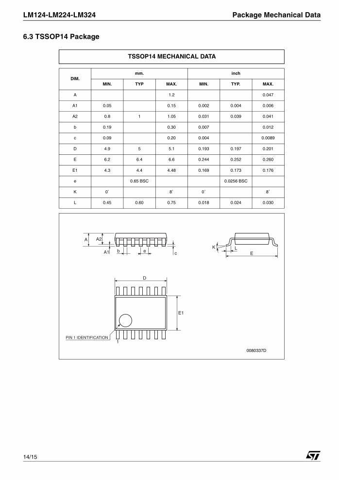
6.3 TSSOP14 Package
DIM.mm. inch
MIN. TYP MAX. MIN. TYP. MAX.
A 1.2 0.047
A1 0.05 0.15 0.002 0.004 0.006
A2 0.8 1 1.05 0.031 0.039 0.041
b 0.19 0.30 0.007 0.012
c 0.09 0.20 0.004 0.0089
D 4.9 5 5.1 0.193 0.197 0.201
E 6.2 6.4 6.6 0.244 0.252 0.260
E1 4.3 4.4 4.48 0.169 0.173 0.176
e 0.65 BSC 0.0256 BSC
K 0˚ 8˚ 0˚ 8˚
L 0.45 0.60 0.75 0.018 0.024 0.030
TSSOP14 MECHANICAL DATA
c Eb
A2A
E1
D
1PIN 1 IDENTIFICATION
A1LK
e
0080337D
14/15
Summary of Changes LM124-LM224-LM324
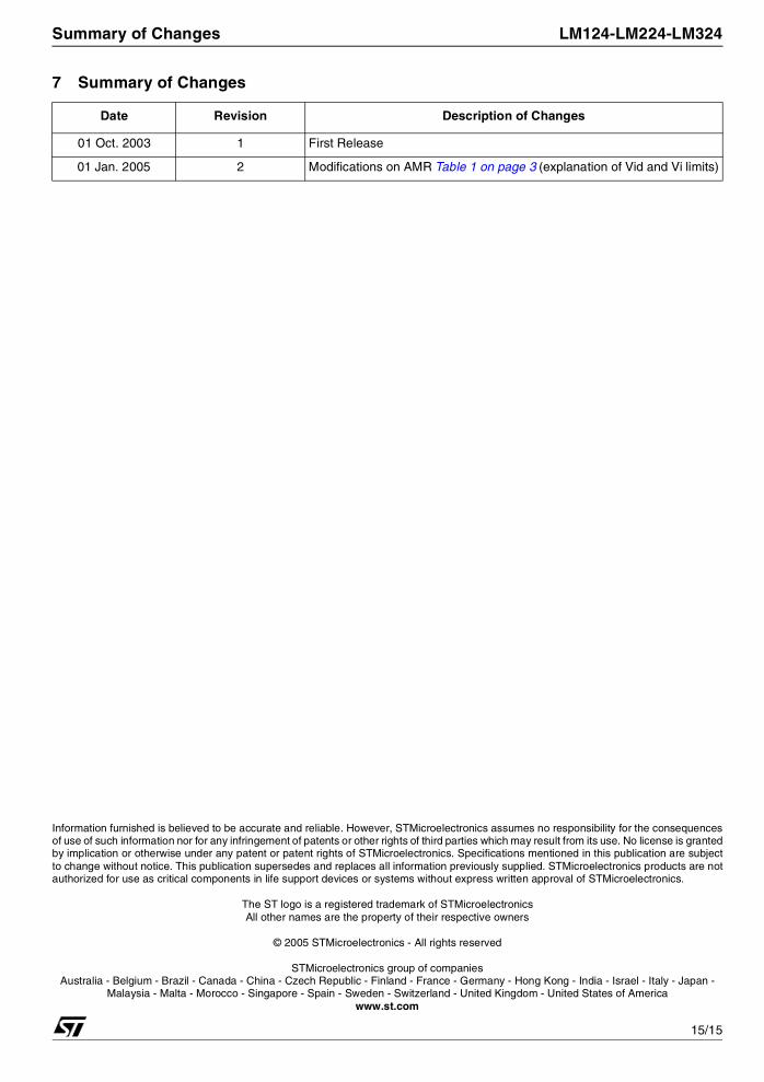
7 Summary of Changes
Date Revision Description of Changes
01 Oct. 2003 1 First Release
01 Jan. 2005 2 Modifications on AMR Table 1 on page 3 (explanation of Vid and Vi limits)
Information furnished is believed to be accurate and reliable. However, STMicroelectronics assumes no responsibility for the consequencesof use of such information nor for any infringement of patents or other rights of third parties which may result from its use. No license is grantedby implication or otherwise under any patent or patent rights of STMicroelectronics. Specifications mentioned in this publication are subjectto change without notice. This publication supersedes and replaces all information previously supplied. STMicroelectronics products are notauthorized for use as critical components in life support devices or systems without express written approval of STMicroelectronics.
The ST logo is a registered trademark of STMicroelectronicsAll other names are the property of their respective owners
© 2005 STMicroelectronics - All rights reserved
STMicroelectronics group of companiesAustralia - Belgium - Brazil - Canada - China - Czech Republic - Finland - France - Germany - Hong Kong - India - Israel - Italy - Japan -
Malaysia - Malta - Morocco - Singapore - Spain - Sweden - Switzerland - United Kingdom - United States of Americawww.st.com
15/15