Embed Size (px)
Citation preview
ILOAD (A)
0.1 1.0 10
84
86
88
90
92
94
96
EF
FIC
IEN
CY
(%
)
PVIN = 3.3V
PVIN
AVIN
EN
SS SGND PGND
SNS
SW
LM2852Y
CSS = 2.7 nF
CIN = 22 PF
VIN = 3.3V
VOUT = 2.5VILOAD = 0A to 2A
CO = 100 PF+LO = 10 PH
Product
Folder
Sample &Buy
Technical
Documents
Tools &
Software
Support &Community
LM2852SNVS325E –JANUARY 2005–REVISED JANUARY 2016
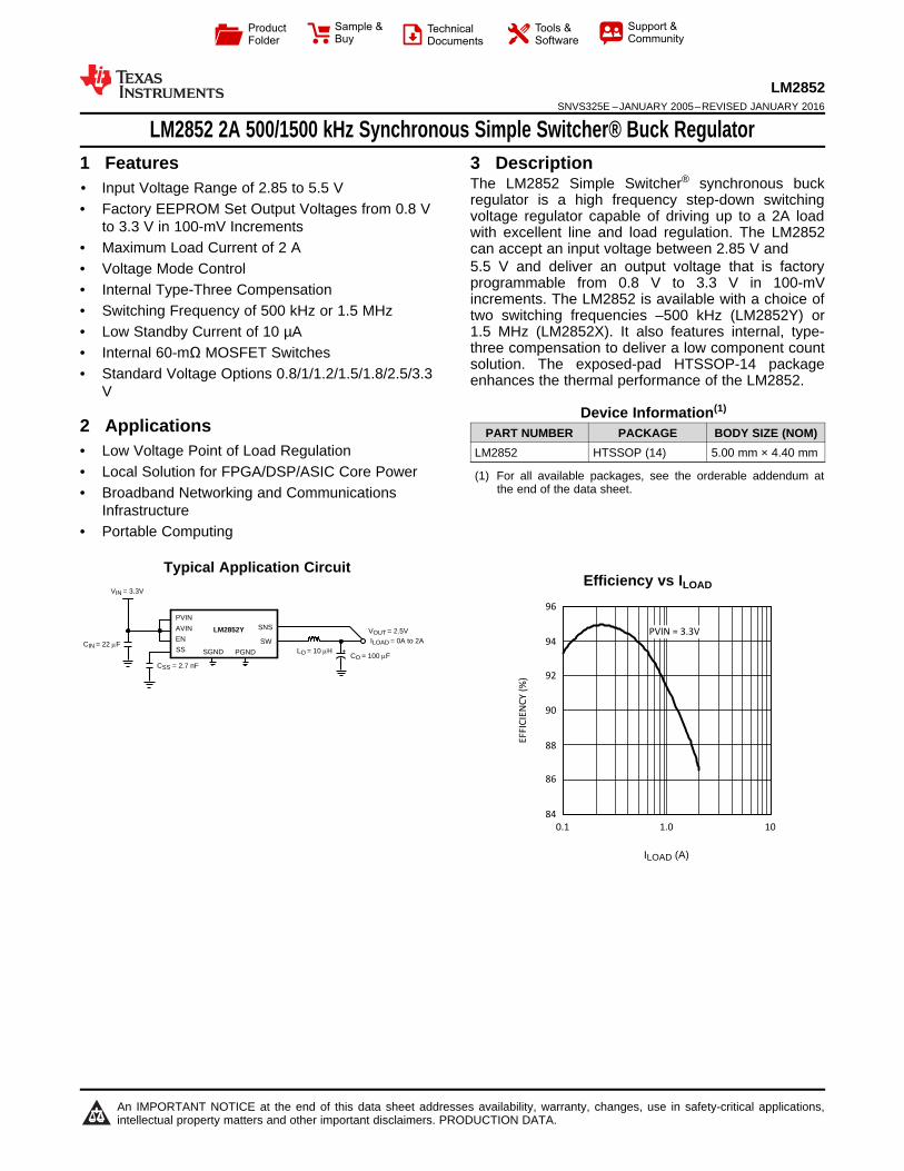
LM2852 2A 500/1500 kHz Synchronous Simple Switcher® Buck Regulator1 Features 3 Description
The LM2852 Simple Switcher® synchronous buck1• Input Voltage Range of 2.85 to 5.5 V
regulator is a high frequency step-down switching• Factory EEPROM Set Output Voltages from 0.8 V voltage regulator capable of driving up to a 2A loadto 3.3 V in 100-mV Increments with excellent line and load regulation. The LM2852
• Maximum Load Current of 2 A can accept an input voltage between 2.85 V and5.5 V and deliver an output voltage that is factory• Voltage Mode Controlprogrammable from 0.8 V to 3.3 V in 100-mV• Internal Type-Three Compensation increments. The LM2852 is available with a choice of
• Switching Frequency of 500 kHz or 1.5 MHz two switching frequencies –500 kHz (LM2852Y) or1.5 MHz (LM2852X). It also features internal, type-• Low Standby Current of 10 µAthree compensation to deliver a low component count• Internal 60-mΩ MOSFET Switchessolution. The exposed-pad HTSSOP-14 package• Standard Voltage Options 0.8/1/1.2/1.5/1.8/2.5/3.3 enhances the thermal performance of the LM2852.
VDevice Information(1)
2 Applications PART NUMBER PACKAGE BODY SIZE (NOM)• Low Voltage Point of Load Regulation LM2852 HTSSOP (14) 5.00 mm × 4.40 mm
• Local Solution for FPGA/DSP/ASIC Core Power (1) For all available packages, see the orderable addendum atthe end of the data sheet.• Broadband Networking and Communications
Infrastructure• Portable Computing
spaceTypical Application Circuit
Efficiency vs ILOAD
1
An IMPORTANT NOTICE at the end of this data sheet addresses availability, warranty, changes, use in safety-critical applications,intellectual property matters and other important disclaimers. PRODUCTION DATA.
LM2852SNVS325E –JANUARY 2005–REVISED JANUARY 2016 www.ti.com
Table of Contents7.3 Feature Description................................................. 111 Features .................................................................. 17.4 Device Functional Modes........................................ 112 Applications ........................................................... 1
8 Application and Implementation ........................ 123 Description ............................................................. 18.1 Application Information............................................ 124 Revision History..................................................... 28.2 Typical Application ................................................. 125 Pin Configuration and Functions ......................... 3
9 Power Supply Recommendations ...................... 186 Specifications......................................................... 410 Layout................................................................... 186.1 Absolute Maximum Ratings ...................................... 4
10.1 Layout Guidelines ................................................. 186.2 ESD Ratings.............................................................. 410.2 Layout Example .................................................... 186.3 Recommended Operating Conditions....................... 4
11 Device and Documentation Support ................. 196.4 Thermal Information .................................................. 411.1 Device Support...................................................... 196.5 Electrical Characteristics........................................... 511.2 Community Resources.......................................... 196.6 LM2852Y Typical Characteristics (500 kHz)............. 711.3 Trademarks ........................................................... 196.7 LM2852X Typical Characteristics (1500 kHz)........... 811.4 Electrostatic Discharge Caution............................ 196.8 LM2852 Typical Characteristics (Both Y and X
Versions) .................................................................... 9 11.5 Glossary ................................................................ 197 Detailed Description ............................................ 10 12 Mechanical, Packaging, and Orderable
Information ........................................................... 197.1 Overview ................................................................. 107.2 Functional Block Diagram ....................................... 10
4 Revision HistoryNOTE: Page numbers for previous revisions may differ from page numbers in the current version.
Changes from Revision D (April 2013) to Revision E Page
• Added ESD Ratings table, Feature Description section, Device Functional Modes, Application and Implementationsection, Power Supply Recommendations section, Layout section, Device and Documentation Support section, andMechanical, Packaging, and Orderable Information section .................................................................................................. 1
2 Submit Documentation Feedback Copyright © 2005–2016, Texas Instruments Incorporated
Product Folder Links: LM2852
EN
SGND
SS
NC
PVIN
PVIN
SNS
NC
NC
PGND
PGND
SW
SW
AVIN
LM2852
1
2
3
4
5
7
6
14
13
12
11
10
8
9
LM2852www.ti.com SNVS325E –JANUARY 2005–REVISED JANUARY 2016
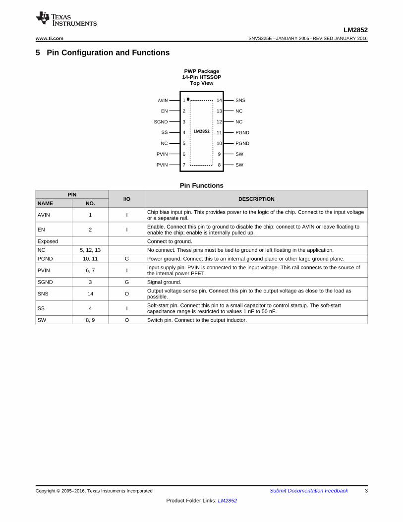
5 Pin Configuration and Functions
PWP Package14-Pin HTSSOP
Top View
Pin FunctionsPIN
I/O DESCRIPTIONNAME NO.
Chip bias input pin. This provides power to the logic of the chip. Connect to the input voltageAVIN 1 I or a separate rail.Enable. Connect this pin to ground to disable the chip; connect to AVIN or leave floating toEN 2 I enable the chip; enable is internally pulled up.
Exposed Connect to ground.NC 5, 12, 13 No connect. These pins must be tied to ground or left floating in the application.PGND 10, 11 G Power ground. Connect this to an internal ground plane or other large ground plane.
Input supply pin. PVIN is connected to the input voltage. This rail connects to the source ofPVIN 6, 7 I the internal power PFET.SGND 3 G Signal ground.
Output voltage sense pin. Connect this pin to the output voltage as close to the load asSNS 14 O possible.Soft-start pin. Connect this pin to a small capacitor to control startup. The soft-startSS 4 I capacitance range is restricted to values 1 nF to 50 nF.
SW 8, 9 O Switch pin. Connect to the output inductor.
Copyright © 2005–2016, Texas Instruments Incorporated Submit Documentation Feedback 3
Product Folder Links: LM2852
LM2852SNVS325E –JANUARY 2005–REVISED JANUARY 2016 www.ti.com
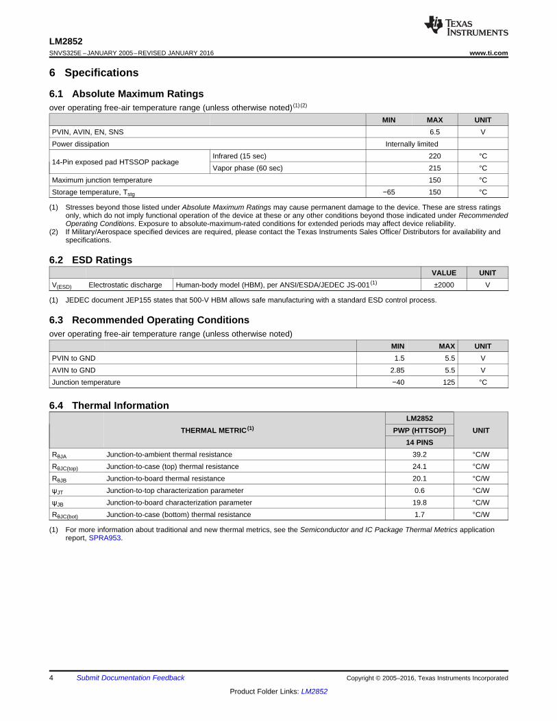
6 Specifications
6.1 Absolute Maximum Ratingsover operating free-air temperature range (unless otherwise noted) (1) (2)
MIN MAX UNITPVIN, AVIN, EN, SNS 6.5 VPower dissipation Internally limited
Infrared (15 sec) 220 °C14-Pin exposed pad HTSSOP package
Vapor phase (60 sec) 215 °CMaximum junction temperature 150 °CStorage temperature, Tstg −65 150 °C
(1) Stresses beyond those listed under Absolute Maximum Ratings may cause permanent damage to the device. These are stress ratingsonly, which do not imply functional operation of the device at these or any other conditions beyond those indicated under RecommendedOperating Conditions. Exposure to absolute-maximum-rated conditions for extended periods may affect device reliability.
(2) If Military/Aerospace specified devices are required, please contact the Texas Instruments Sales Office/ Distributors for availability andspecifications.
6.2 ESD RatingsVALUE UNIT
V(ESD) Electrostatic discharge Human-body model (HBM), per ANSI/ESDA/JEDEC JS-001 (1) ±2000 V
(1) JEDEC document JEP155 states that 500-V HBM allows safe manufacturing with a standard ESD control process.
6.3 Recommended Operating Conditionsover operating free-air temperature range (unless otherwise noted)
MIN MAX UNITPVIN to GND 1.5 5.5 VAVIN to GND 2.85 5.5 VJunction temperature −40 125 °C
6.4 Thermal InformationLM2852
THERMAL METRIC (1) PWP (HTTSOP) UNIT14 PINS
RθJA Junction-to-ambient thermal resistance 39.2 °C/WRθJC(top) Junction-to-case (top) thermal resistance 24.1 °C/WRθJB Junction-to-board thermal resistance 20.1 °C/WψJT Junction-to-top characterization parameter 0.6 °C/WψJB Junction-to-board characterization parameter 19.8 °C/WRθJC(bot) Junction-to-case (bottom) thermal resistance 1.7 °C/W
(1) For more information about traditional and new thermal metrics, see the Semiconductor and IC Package Thermal Metrics applicationreport, SPRA953.
4 Submit Documentation Feedback Copyright © 2005–2016, Texas Instruments Incorporated
Product Folder Links: LM2852
LM2852www.ti.com SNVS325E –JANUARY 2005–REVISED JANUARY 2016
6.5 Electrical CharacteristicsAVIN = PVIN = 5 V unless otherwise indicated under the Test Conditions column. Limits apply over the junction temperature(TJ) range of –40°C to 125°C (unless otherwise noted). Minimum and Maximum limits are ensured through test, design, orstatistical correlation. Typical values represent the most likely parametric norm at TJ = 25°C, and are provided for referencepurposes only.
PARAMETER TEST CONDITIONS MIN TYP MAX UNITSYSTEM PARAMETERS
VOUT = 0.8-V option 0.782 0.818VOUT = 1-V option 0.9775 1.0225VOUT = 1.2-V option 1.173 1.227VOUT = 1.5-V option 1.4663 1.5337VoltageVOUT Vtolerance (1) VOUT = 1.8-V option 1.7595 1.8405VOUT = 2.5-V option 2.4437 2.5563VOUT = 3-V option 2.9325 3.0675VOUT = 3.3-V option 3.2257 3.3743
TJ = –40°C toVOUT = 0.8 V, 1 V, 1.2 V, 1.5 V, 0.6%125°C1.8 V or 2.5 V,2.85 V ≤ AVIN ≤ 5.5 V TJ = 25°C 0.2%
ΔVOUT/ ΔAVIN Line regulation (1)TJ = –40°C to 0.6%VOUT = 3.3 V, 125°C
3.5 V ≤ AVIN ≤ 5.5 VTJ = 25°C 0.2%
ΔVOUT/ΔIO Load regulation Normal operation TJ = 25°C 8 mV/ATJ = –40°C to 2.85125°CRising VTJ = 25°C 2.47
VON UVLO threshold (AVIN)TJ = –40°C to 85 210125°CFalling hysteresis mVTJ = 25°C 150TJ = –40°C to 140125°CrDSON-P PFET ON resistance Isw = 2 A mΩTJ = 25°C 75TJ = –40°C to 120125°CrDSON-N NFET ON resistance Isw = 2 A mΩTJ = 25°C 55
RSS Soft-start resistance TJ = 25°C 400 kΩTJ = –40°C to 2.75 4.95125°CLM2852XTJ = 25°C 4Peak current limitICL Athreshold TJ = –40°C to 2.25 3.65125°CLM2852YTJ = 25°C 3TJ = –40°C to 2125°CIQ Operating current Non-switching mATJ = 25°C 0.85TJ = –40°C to 25Shutdown quiescent 125°CISD EN = 0 V µAcurrentTJ = 25°C 10
RSNS Sense pin resistance TJ = 25°C 400 kΩ
(1) VOUT measured in a non-switching, closed-loop configuration at the SNS pin.
Copyright © 2005–2016, Texas Instruments Incorporated Submit Documentation Feedback 5
Product Folder Links: LM2852
LM2852SNVS325E –JANUARY 2005–REVISED JANUARY 2016 www.ti.com
Electrical Characteristics (continued)AVIN = PVIN = 5 V unless otherwise indicated under the Test Conditions column. Limits apply over the junction temperature(TJ) range of –40°C to 125°C (unless otherwise noted). Minimum and Maximum limits are ensured through test, design, orstatistical correlation. Typical values represent the most likely parametric norm at TJ = 25°C, and are provided for referencepurposes only.
PARAMETER TEST CONDITIONS MIN TYP MAX UNITPWM
TJ = –40°C to 1050 1825125°CLM2852X 1500-kHz option. kHzTJ = 25°C 1500
fosc TJ = –40°C to 325 625125°CLM2852Y 500-kHz option. kHzTJ = 25°C 500
Drange Duty cycle 0% 100%ENABLE CONTROL (2)
EN pin minimum high % ofVIH 75input AVINEN pin maximum low % ofVIL 25input AVIN
IEN EN pin pullup current EN = 0 V TJ = 25°C 1.2 µATHERMAL CONTROLSTSD TJ for thermal shutdown TJ = 25°C 165 °C
Hysteresis for thermalTSD-HYS TJ = 25°C 10 °Cshutdown
(2) The enable pin is internally pulled up, so the LM2852 is automatically enabled unless an external enable voltage is applied.
6 Submit Documentation Feedback Copyright © 2005–2016, Texas Instruments Incorporated
Product Folder Links: LM2852
0.1 1.0 10
87
88
89
90
91
92
93
94
95
EF
FIC
IEN
CY
(%
)
ILOAD (A)
PVIN = 5.0V
-50 -25 0 25 50 75 100 125 150
TEMPERATURE (oC)
480
490
500
510
520
530
540
550
560
FR
EQ
UE
NC
Y (
kH
z)
VIN = 3.3V
VIN = 5V
0.1 1.0 10
76
78
80
82
84
86
88
90
92
EF
FIC
IEN
CY
(%
)
ILOAD (A)
PVIN = 3.3V
PVIN = 5.0V
0.1 1.0 1084
86
88
90
92
94
96
PVIN = 3.3V
ILOAD (A)
EF
FIC
IEN
CY
(%
)
PVIN = 5.0V
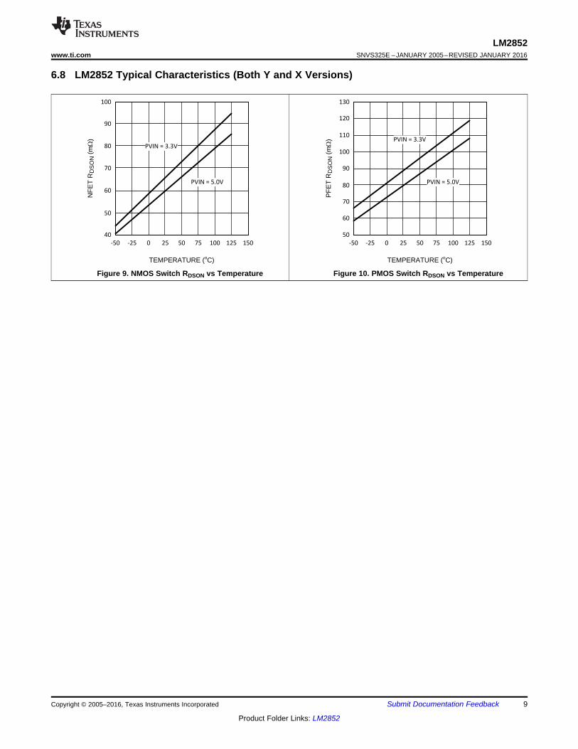
LM2852www.ti.com SNVS325E –JANUARY 2005–REVISED JANUARY 2016
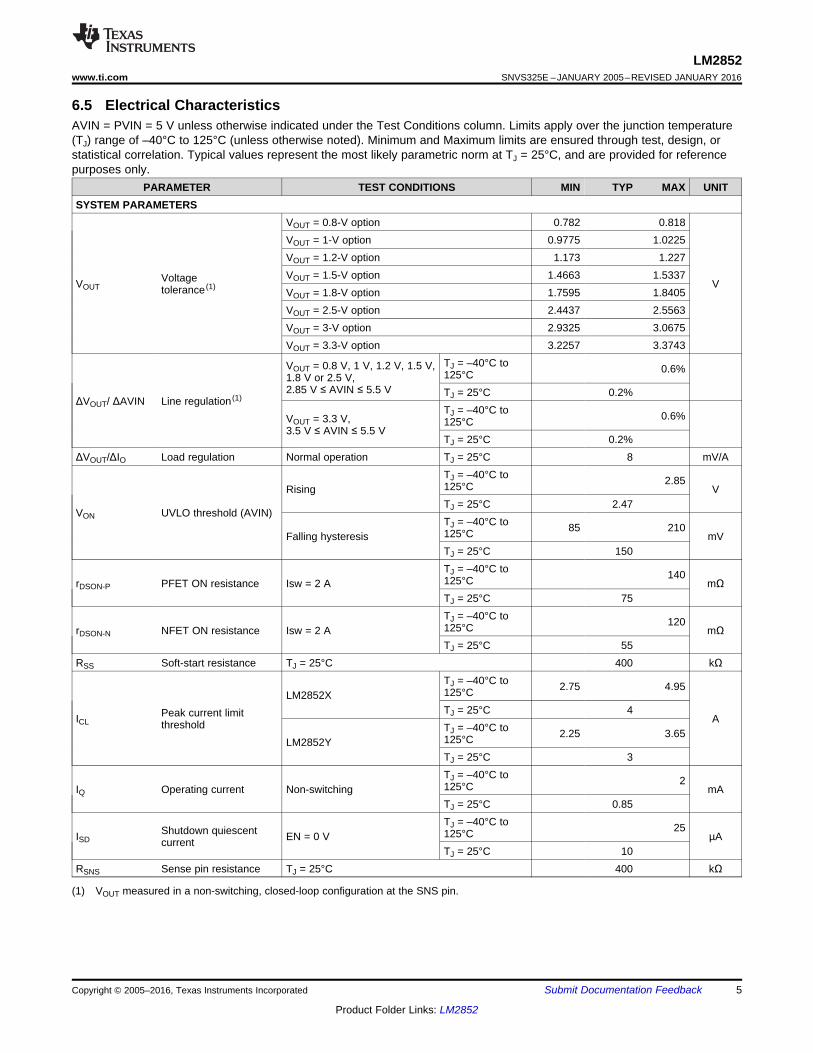
6.6 LM2852Y Typical Characteristics (500 kHz)
Figure 2. Efficiency vs ILoad VOUT = 2.5 VFigure 1. Efficiency vs ILoad VOUT = 1.5 V
Figure 4. Frequency vs TemperatureFigure 3. Efficiency vs ILoad VOUT = 3.3 V
Copyright © 2005–2016, Texas Instruments Incorporated Submit Documentation Feedback 7
Product Folder Links: LM2852
0.1 1.0 10
50
55
60
65
70
75
80
85
90
EF
FIC
IEN
CY
(%
)
ILOAD (A)
PVIN = 5.0V
-50 -25 0 25 50 75 80 85 90
TEMPERATURE (oC)
FR
EQ
UE
NC
Y (
kHz)
PVIN = 3.3V
PVIN = 5.0V
1200
1250
1300
1350
1400
1450
1500
1550
1600
0.1 1.0 10
45
50
55
60
65
70
75
80
85
EF
FIC
IEN
CY
(%
)
ILOAD (A)
PVIN = 3.3V
PVIN = 5.0V
ILOAD (A)
0.1 1.0 10
40
50
60
70
80
90
100
EF
FIC
IEN
CY
(%
)
PVIN = 3.3V
PVIN = 5.0V
LM2852SNVS325E –JANUARY 2005–REVISED JANUARY 2016 www.ti.com
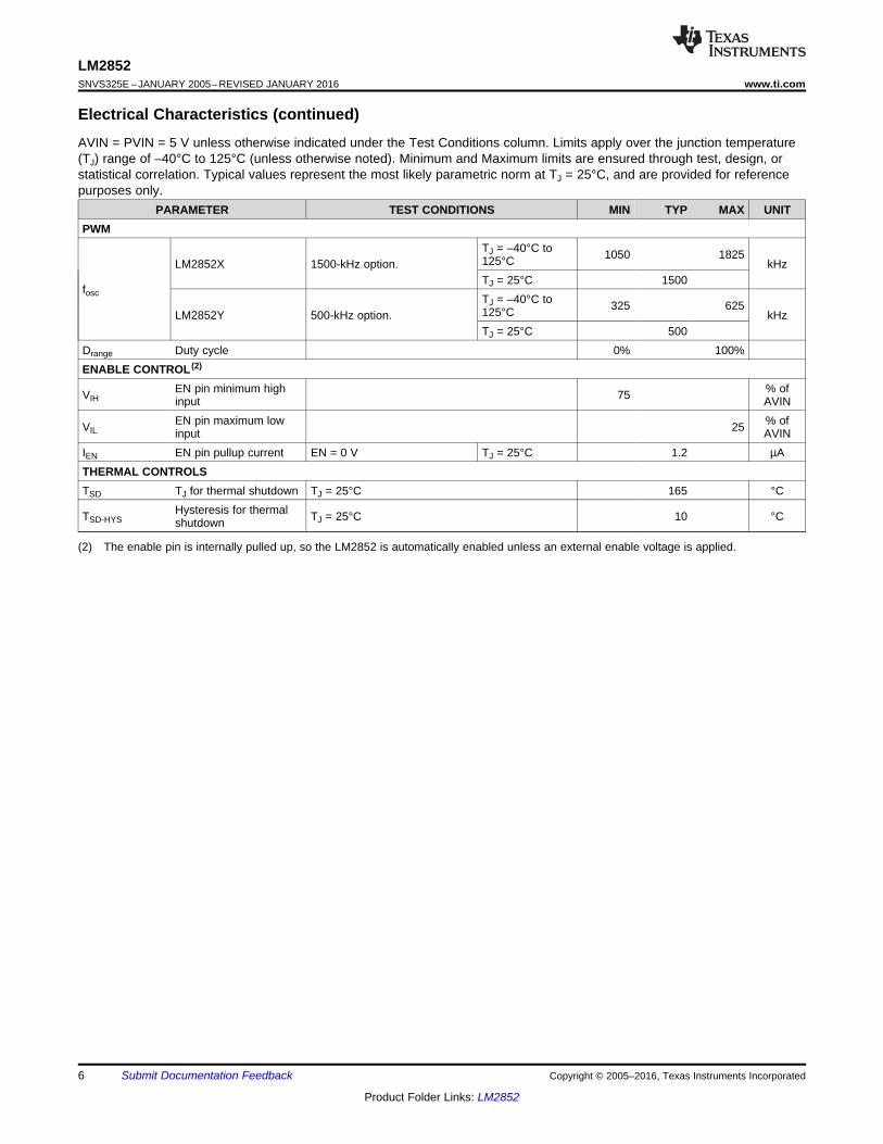
6.7 LM2852X Typical Characteristics (1500 kHz)
Figure 5. Efficiency vs ILoad VOUT = 1.5 V Figure 6. Efficiency vs ILoad VOUT = 2.5 V
Figure 8. Frequency vs TemperatureFigure 7. Efficiency vs ILoad VOUT = 3.3 V
8 Submit Documentation Feedback Copyright © 2005–2016, Texas Instruments Incorporated
Product Folder Links: LM2852
-50 -25 0 25 50 75 100 125 150
TEMPERATURE (oC)
40
50
60
70
80
90
100
NF
ET
RD
SO
N (
m:
)
PVIN = 3.3V
PVIN = 5.0V
-50 -25 0 25 50 75 100 125 150
TEMPERATURE (oC)
50
60
70
80
90
100
110
120
130
PF
ET
RD
SO
N (
m:
) PVIN = 3.3V
PVIN = 5.0V
LM2852www.ti.com SNVS325E –JANUARY 2005–REVISED JANUARY 2016
6.8 LM2852 Typical Characteristics (Both Y and X Versions)
Figure 9. NMOS Switch RDSON vs Temperature Figure 10. PMOS Switch RDSON vs Temperature
Copyright © 2005–2016, Texas Instruments Incorporated Submit Documentation Feedback 9
Product Folder Links: LM2852
Ramp and ClockGenerator
AVIN
EN
PVIN
GateDrive
SW
PGND
+-+
-
SS
SNS
ErrorAmp
PWMComp
OscillatorReference
UVLO DAC
Zc2
400 k:
200 k:200 k:
20 pF
SGND
Zc1
Current Limit
LM2852SNVS325E –JANUARY 2005–REVISED JANUARY 2016 www.ti.com
7 Detailed Description
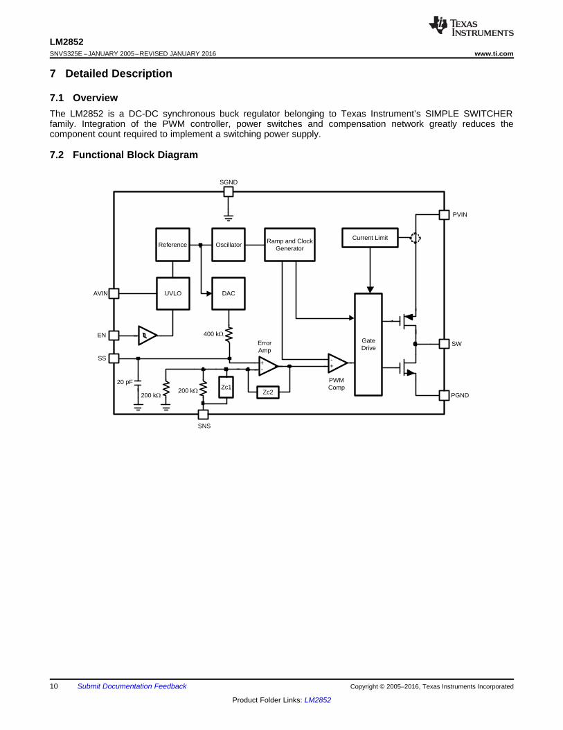
7.1 OverviewThe LM2852 is a DC-DC synchronous buck regulator belonging to Texas Instrument’s SIMPLE SWITCHERfamily. Integration of the PWM controller, power switches and compensation network greatly reduces thecomponent count required to implement a switching power supply.
7.2 Functional Block Diagram
10 Submit Documentation Feedback Copyright © 2005–2016, Texas Instruments Incorporated
Product Folder Links: LM2852
CSS = 3.3 nF
CO = 100 PF
PVIN
AVIN
EN
SS SGND PGND
SNS
SW
LM2852Y
+
VOUT = 1.5VILOAD = 0A to 2A
LO = 10 PH
CIN = 47 PF1 PF
PVIN = 3.3V
AVIN = 5V
LM2852www.ti.com SNVS325E –JANUARY 2005–REVISED JANUARY 2016
7.3 Feature Description
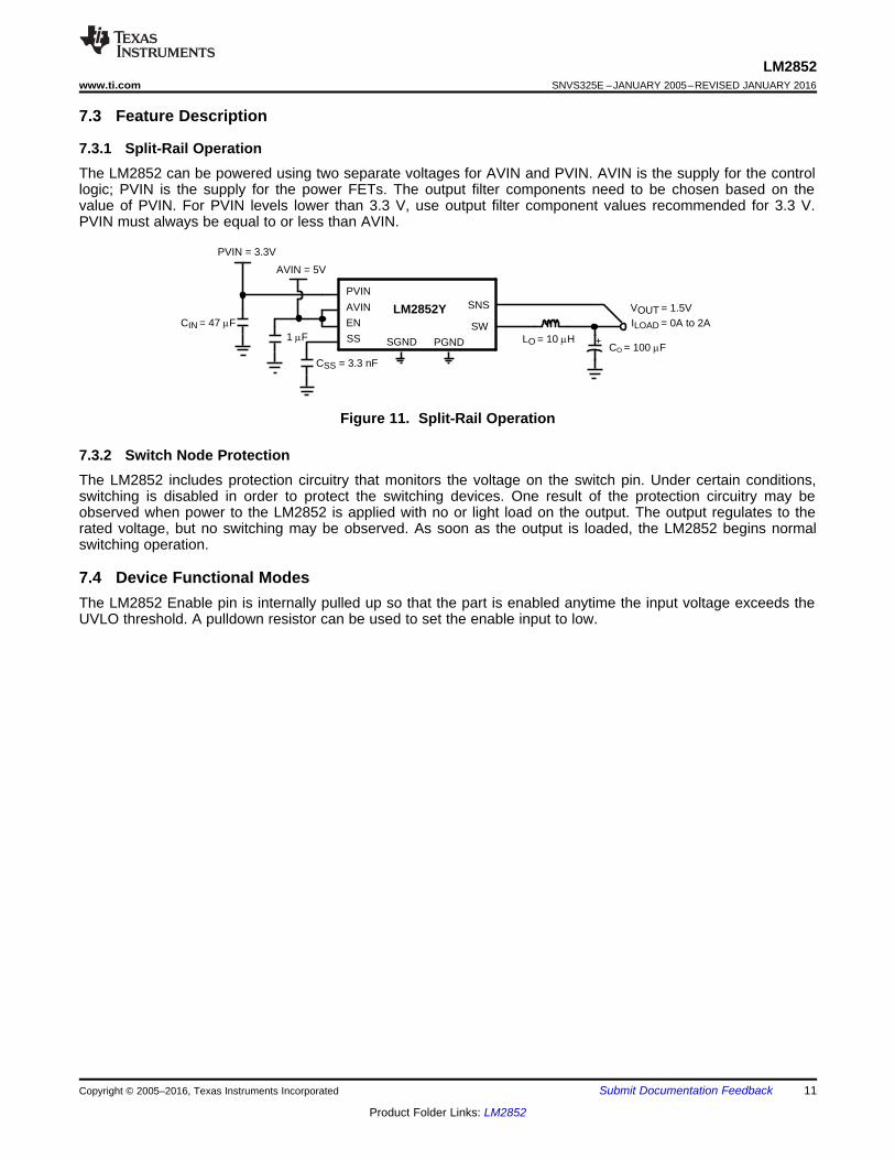
7.3.1 Split-Rail OperationThe LM2852 can be powered using two separate voltages for AVIN and PVIN. AVIN is the supply for the controllogic; PVIN is the supply for the power FETs. The output filter components need to be chosen based on thevalue of PVIN. For PVIN levels lower than 3.3 V, use output filter component values recommended for 3.3 V.PVIN must always be equal to or less than AVIN.
Figure 11. Split-Rail Operation
7.3.2 Switch Node ProtectionThe LM2852 includes protection circuitry that monitors the voltage on the switch pin. Under certain conditions,switching is disabled in order to protect the switching devices. One result of the protection circuitry may beobserved when power to the LM2852 is applied with no or light load on the output. The output regulates to therated voltage, but no switching may be observed. As soon as the output is loaded, the LM2852 begins normalswitching operation.
7.4 Device Functional ModesThe LM2852 Enable pin is internally pulled up so that the part is enabled anytime the input voltage exceeds theUVLO threshold. A pulldown resistor can be used to set the enable input to low.
Copyright © 2005–2016, Texas Instruments Incorporated Submit Documentation Feedback 11
Product Folder Links: LM2852

IRMS = ILOAD D(1-D)
CSS
PVIN
AVIN
EN
SS SGND PGND
SNS
SW
LM2852
+
VOUT = 1.8VILOAD = 0A to 2A
LOCIN
VIN = 3.3V
CfRf
CINXCO
U1
LM2852SNVS325E –JANUARY 2005–REVISED JANUARY 2016 www.ti.com
8 Application and Implementation
NOTEInformation in the following applications sections is not part of the TI componentspecification, and TI does not warrant its accuracy or completeness. TI’s customers areresponsible for determining suitability of components for their purposes. Customers mustvalidate and test their design implementation to confirm system functionality.
8.1 Application InformationThe LM2852 is a DC-DC synchronous buck regulator capable of driving a maximum load current of 2A, with aninput range of 2.85 V to 5.5 V and a variable output range of 0.8 V to 3.3 V. Figure 12 is a schematic example ofa typical application.
8.2 Typical Application
Figure 12. LM2852 Example Circuit Schematic
8.2.1 Design RequirementsA typical application requires only four components: an input capacitor, a soft-start capacitor, an output filtercapacitor and an output filter inductor. To properly size the components for the application, the designer needsthe following parameters: input voltage range, output voltage, output current range, and required switchingfrequency. These four main parameters affect the choices of component available to achieve a proper systembehavior.
8.2.2 Detailed Design Procedure
8.2.2.1 Input Capacitor (CIN)Fast switching of large currents in the buck converter places a heavy demand on the voltage source supplyingPVIN. The input capacitor, CIN, supplies extra charge when the switcher needs to draw a burst of current fromthe supply. The RMS current rating and the voltage rating of the CIN capacitor are therefore important in theselection of CIN. The RMS current specification can be approximated by Equation 1:
where• D is the duty cycle, VOUT/VIN. CIN also provides filtering of the supply. (1)
Trace resistance and inductance degrade the benefits of the input capacitor, so CIN must be placed very close toPVIN in the layout. A 22-µF or 47-µF ceramic capacitor is typically sufficient for CIN. In parallel with the largeinput capacitance a smaller capacitor may be added such as a 1-µF ceramic for higher frequency filtering.
12 Submit Documentation Feedback Copyright © 2005–2016, Texas Instruments Incorporated
Product Folder Links: LM2852
't = CI'V
= 100 PF3A3V
= 100 Ps
LM2852www.ti.com SNVS325E –JANUARY 2005–REVISED JANUARY 2016
Typical Application (continued)8.2.2.2 Soft-Start Capacitor (CSS)The DAC that sets the reference voltage of the error amp sources a current through a resistor to set thereference voltage. The reference voltage is one half of the output voltage of the switcher due to the 200 kΩdivider connected to the SNS pin. Upon start-up, the output voltage of the switcher tracks the reference voltagewith a two to one ratio as the DAC current charges the capacitance connected to the reference voltage node.Internal capacitance of 20 pF is permanently attached to the reference voltage node which is also connected tothe soft-start pin, SS. Adding a soft-start capacitor externally increases the time it takes for the output voltage toreach its final level.
The charging time required for the reference voltage can be estimated using the RC time constant of the DACresistor and the capacitance connected to the SS pin. Three RC time constant periods are needed for thereference voltage to reach 95% of its final value. The actual start-up time varies with differences in the DACresistance and higher-order effects.
If little or no soft-start capacitance is connected, then the start-up time may be determined by the time requiredfor the current limit current to charge the output filter capacitance. The capacitor charging equation I = C ΔV/Δtcan be used to estimate the start-up time in this case. For example, a part with a 3-V output, a 100-µF outputcapacitance and a 3-A current limit threshold would require a time of 100 µs, seen in Equation 2:
(2)
Since it is undesirable for the power supply to start up in current limit, a soft-start capacitor must be chosen toforce the LM2852 to start up in a more controlled fashion based on the charging of the soft-start capacitance. Inthis example, suppose a 3 ms start time is desired. Three time constants are required for charging the soft-startcapacitor to 95% of the final reference voltage. So in this case RC = 1 ms. The DAC resistor, R, is 400 kΩ so Ccan be calculated to be 2.5 nF. A 2.7-nF ceramic capacitor can be chosen to yield approximately a 3 ms start-uptime.
8.2.2.3 Soft-Start Capacitor (CSS) and Fault ConditionsVarious fault conditions such as short circuit and UVLO of the LM2852 activate internal circuitry designed tocontrol the voltage on the soft-start capacitor. For example, during a short circuit current limit event, the outputvoltage typically falls to a low voltage. During this time, the soft-start voltage is forced to track the output so thatonce the short is removed, the LM2852 can restart gracefully from whatever voltage the output reached duringthe short circuit event. The range of soft-start capacitors is therefore restricted to values 1 nF to 50 nF.
8.2.2.4 CompensationThe LM2852 provides a highly integrated solution to power supply design. The compensation of the LM2852,which is type-three, is included on-chip. The benefit to integrated compensation is straightforward, simple powersupply design. Since the output filter capacitor and inductor values impact the compensation of the control loop,the range of L, C and CESR values is restricted in order to ensure stability.
Copyright © 2005–2016, Texas Instruments Incorporated Submit Documentation Feedback 13
Product Folder Links: LM2852
LM2852SNVS325E –JANUARY 2005–REVISED JANUARY 2016 www.ti.com
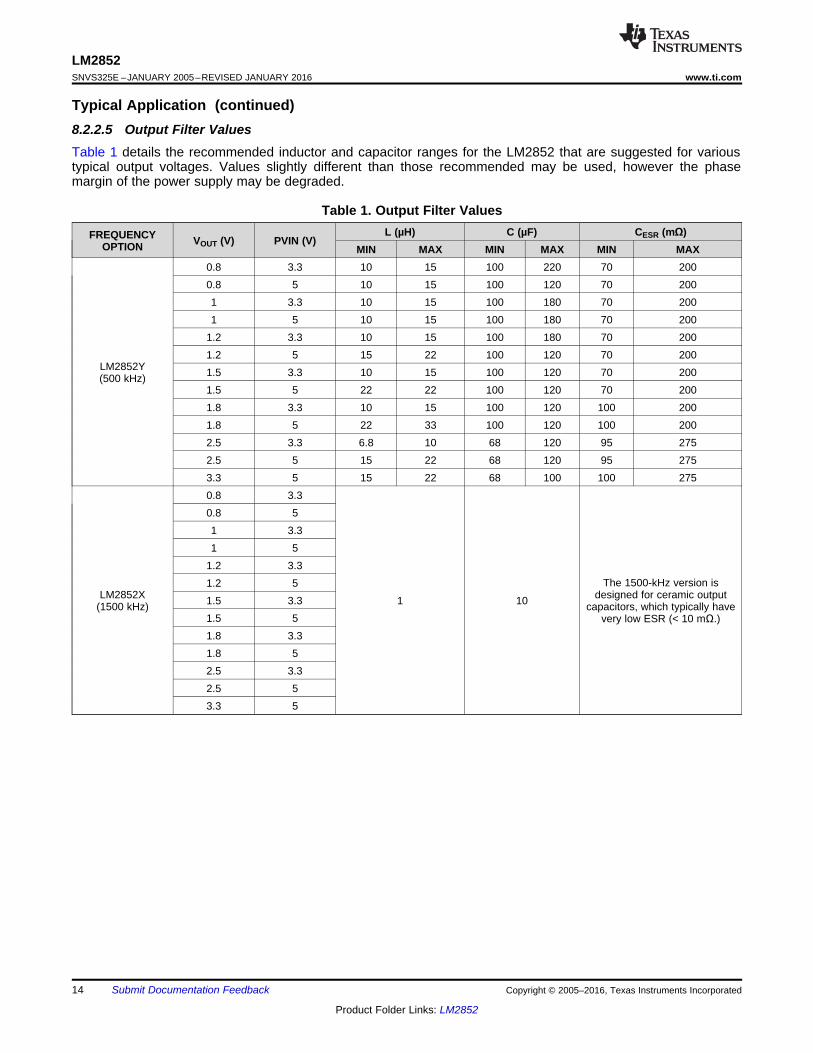
Typical Application (continued)8.2.2.5 Output Filter ValuesTable 1 details the recommended inductor and capacitor ranges for the LM2852 that are suggested for varioustypical output voltages. Values slightly different than those recommended may be used, however the phasemargin of the power supply may be degraded.
Table 1. Output Filter ValuesL (µH) C (µF) CESR (mΩ)FREQUENCY VOUT (V) PVIN (V)OPTION MIN MAX MIN MAX MIN MAX
0.8 3.3 10 15 100 220 70 2000.8 5 10 15 100 120 70 2001 3.3 10 15 100 180 70 2001 5 10 15 100 180 70 200
1.2 3.3 10 15 100 180 70 2001.2 5 15 22 100 120 70 200
LM2852Y 1.5 3.3 10 15 100 120 70 200(500 kHz)1.5 5 22 22 100 120 70 2001.8 3.3 10 15 100 120 100 2001.8 5 22 33 100 120 100 2002.5 3.3 6.8 10 68 120 95 2752.5 5 15 22 68 120 95 2753.3 5 15 22 68 100 100 2750.8 3.30.8 51 3.31 5
1.2 3.3The 1500-kHz version is1.2 5
LM2852X designed for ceramic output1.5 3.3 1 10(1500 kHz) capacitors, which typically have1.5 5 very low ESR (< 10 mΩ.)1.8 3.31.8 52.5 3.32.5 53.3 5
14 Submit Documentation Feedback Copyright © 2005–2016, Texas Instruments Incorporated
Product Folder Links: LM2852
'IL =500 kHz x 15 PH
1.2Vx
5V(5V - 1.2V)
= 121.6 mA
'IL =f x L
D x (VIN - VOUT)
LM2852www.ti.com SNVS325E –JANUARY 2005–REVISED JANUARY 2016
8.2.2.6 Choosing an Inductance ValueThe current ripple present in the output filter inductor is determined by the input voltage, output voltage, switchingfrequency and inductance according to Equation 3:
where• ΔIL is the peak-to-peak current ripple.• D is the duty cycle VOUT/VIN.
• VIN is the input voltage applied to the PVIN pin.• VOUT is the output voltage of the switcher.• f is the switching frequency.• L is the inductance of the output filter inductor. (3)
Knowing the current ripple is important for inductor selection since the peak current through the inductor is theload current plus one half the ripple current. Care must be taken to ensure the peak inductor current does notreach a level high enough to trip the current limit circuitry of the LM2852.
As an example, consider a 5-V to 1.2-V conversion and a 500-kHz switching frequency. According to Table 1, a15-µH inductor may be used. Calculating the expected peak-to-peak ripple, as seen in Equation 4.
(4)
The maximum inductor current for a 2-A load would therefore be 2 A plus 60.8 mA, 2.0608 A. As shown in theripple equation, the current ripple is inversely proportional to inductance.
8.2.2.7 Output Filter InductorsOnce the inductance value is chosen, the key parameter for selecting the output filter inductor is its saturationcurrent (Isat) specification. Typically Isat is given by the manufacturer as the current at which the inductance of thecoil falls to a certain percentage of the nominal inductance. The Isat of an inductor used in an application must begreater than the maximum expected inductor current to avoid saturation. Table 2 lists the inductors that may besuitable in LM2852 applications.
Table 2. LM2852 Output Filter InductorsINDUCTANCE (µH) PART NUMBER VENDOR
1 DO1608C-102 Coilcraft1 DO1813P-102HC Coilcraft
6.8 DO3316P-682 Coilcraft7 MSS1038-702NBC Coilcraft10 DO3316P-103 Coilcraft10 MSS1038-103NBC Coilcraft12 MSS1038-123NBC Coilcraft15 D03316P-153 Coilcraft15 MSS1038-153NBC Coilcraft18 MSS1038-183NBC Coilcraft22 DO3316P-223 Coilcraft22 MSS1038-223NBC Coilcraft22 DO3340P-223 Coilcraft27 MSS1038-273NBC Coilcraft33 MSS1038-333NBC Coilcraft33 DO3340P-333 Coilcraft
Copyright © 2005–2016, Texas Instruments Incorporated Submit Documentation Feedback 15
Product Folder Links: LM2852

LM2852SNVS325E –JANUARY 2005–REVISED JANUARY 2016 www.ti.com
8.2.2.8 Output Filter CapacitorsThe capacitors that may be used in the output filter with the LM2852 are limited in value and ESR rangeaccording to Table 1. Table 3 lists some examples of capacitors that can typically be used in an LM2852application.
Table 3. LM2852 Output Filter CapacitorsCAPACITANCE (µF) PART NUMBER CHEMISTRY VENDOR
10 GRM31MR61A106KE19 Ceramic Murata10 GRM32DR61E106K Ceramic Murata68 595D686X_010C2T Tantalum Vishay - Sprague68 595D686X_016D2T Tantalum Vishay - Sprague100 595D107X_6R3C2T Tantalum Vishay - Sprague100 595D107X_016D2T Tantalum Vishay - Sprague100 NOSC107M004R0150 Niobium Oxide AVX100 NOSD107M006R0100 Niobium Oxide AVX120 595D127X_004C2T Tantalum Vishay - Sprague120 595D127X_010D2T Tantalum Vishay - Sprague150 595D157X_004C2T Tantalum Vishay - Sprague150 595D157X_016D2T Tantalum Vishay - Sprague150 NOSC157M004R0150 Niobium Oxide AVX150 NOSD157M006R0100 Niobium Oxide AVX220 595D227X_004D2T Tantalum Vishay - Sprague220 NOSD227M004R0100 Niobium Oxide AVX220 NOSE227M006R0100 Niobium Oxide AVX
Table 4. Bill of Materials for 500kHz (LM2852Y) 3.3 VIN to 1.8 VOUT ConversionID PART NUMBER TYPE SIZE PARAMETERS QTY VENDORU1 LM2852YMXA-1.8 2-A buck HTSSOP-14 1 TILO DO3316P-153 Inductor 15 µH 1 Coilcraft
CO* 595D107X_6R3C2T Capacitor Case Code “C” 100 µF ±20% 1 Vishay-SpragueCIN GRM32ER60J476ME20B Capacitor 1210 47 µF/X5R/6.3V 1 MurataCINX GRM21BR71C105KA01B Capacitor 0805 1 µF/X7R/16V 1 MurataCSS VJ0805Y272KXXA Capacitor 0805 2.7 nF ±10% 1 Vishay-VitramonRf CRCW060310R0F Resistor 0603 10 Ω ±10% 1 Vishay-DaleCf GRM21BR71C105KA01B Capacitor 0805 1 µF/X7R/16V 1 Murata
Table 5. Bill of Materials for 1500-kHz (LM2852X) 3.3-V to 1.8-V ConversionID PART NUMBER TYPE SIZE PARAMETERS QTY VENDORU1 LM2852XMXA-1.8 2-A buck HTSSOP-14 1 TIL0 DO1813P-102HC Inductor 1 µH 1 CoilcraftC0 GRM32DR61E106K Capacitor 1210 10 µF/X5R/25V 1 MurataCIN GRM32ER60J476ME20B Capacitor 1210 47 µF/X5R/6.3V 1 MurataCINX GRM21BR71C105KA01B Capacitor 0805 1 µF/X7R/16V 1 MurataCSS VJ0805Y272KXXA Capacitor 0805 2.7 nF ±10% 1 Vishay-VitramonRf CRCW060310R0F Resistor 0603 10 Ω ±10% 1 Vishay-DaleCf GRM21BR71C105KA01B Capacitor 0805 1 µF/X7R/16V 1 Murata
16 Submit Documentation Feedback Copyright © 2005–2016, Texas Instruments Incorporated
Product Folder Links: LM2852
2.5 3 3.5 4 4.5 5 5.5
VIN (V)
5
7
9
11
13
15
17
I Q S
HU
TD
OW
N (P
A)
25oC
85oC
125oC
-40oC
2.5 3 3.5 4 4.5 5 5.5
VIN (V)
500
600
700
800
900
1000
1100
I Q (P
A)
25oC
85oC
125oC
-40oC
LM2852www.ti.com SNVS325E –JANUARY 2005–REVISED JANUARY 2016
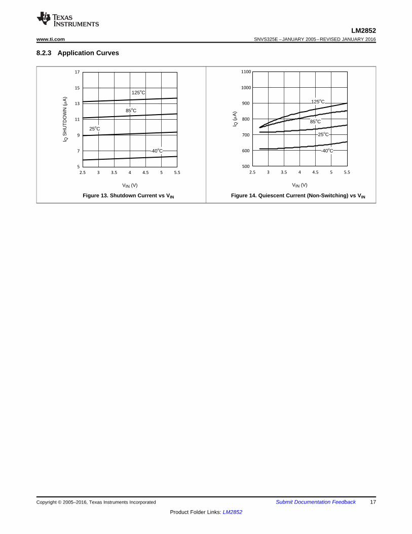
8.2.3 Application Curves
Figure 13. Shutdown Current vs VIN Figure 14. Quiescent Current (Non-Switching) vs VIN
Copyright © 2005–2016, Texas Instruments Incorporated Submit Documentation Feedback 17
Product Folder Links: LM2852
LM2852SNVS325E –JANUARY 2005–REVISED JANUARY 2016 www.ti.com
9 Power Supply RecommendationsThe LM2852 is designed to operate from various DC power supplies. If so, VIN input must be protected fromreversal voltage and voltage dump over 6.5 V. The impedance of the input supply rail must be low enough thatthe input current transient does not cause drop below VIN UVLO level. If the input supply is connected by usinglong wires, additional bulk capacitance may be required in addition to normal input capacitor.
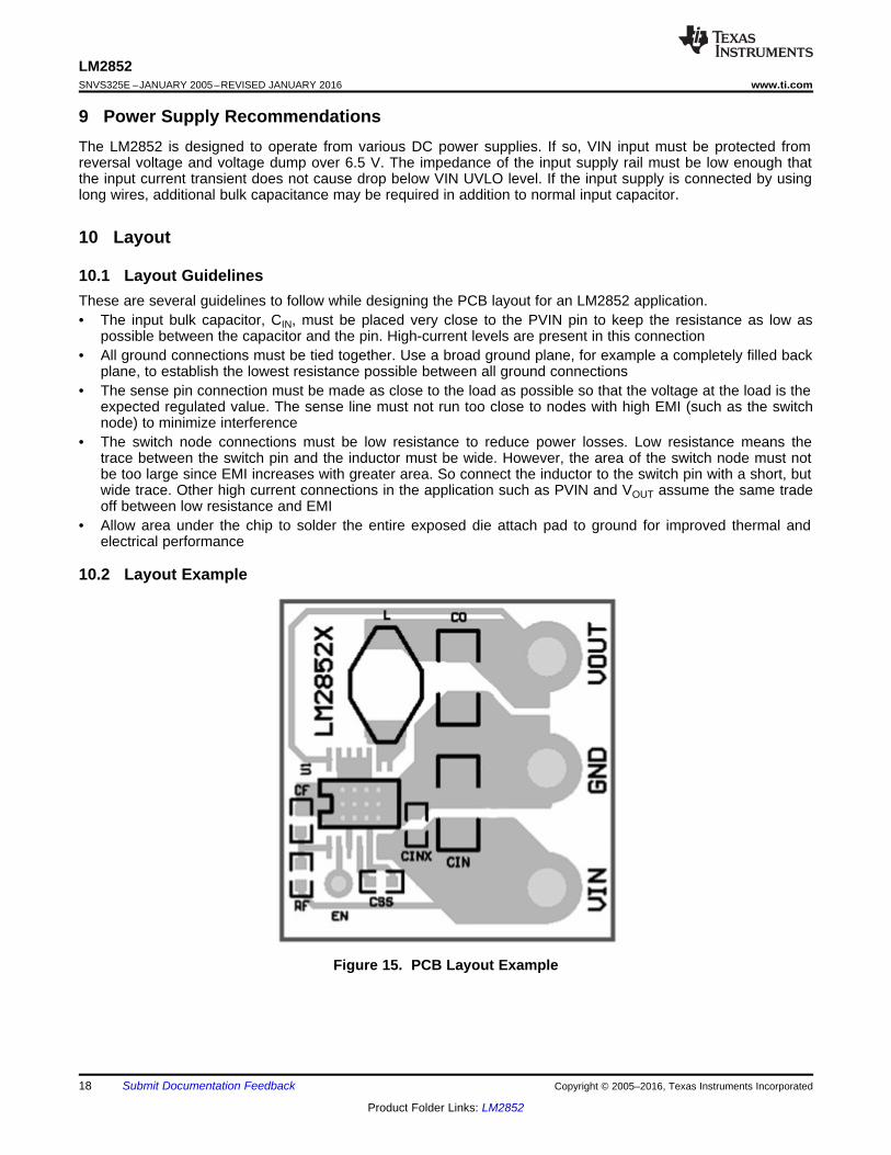
10 Layout
10.1 Layout GuidelinesThese are several guidelines to follow while designing the PCB layout for an LM2852 application.• The input bulk capacitor, CIN, must be placed very close to the PVIN pin to keep the resistance as low as
possible between the capacitor and the pin. High-current levels are present in this connection• All ground connections must be tied together. Use a broad ground plane, for example a completely filled back
plane, to establish the lowest resistance possible between all ground connections• The sense pin connection must be made as close to the load as possible so that the voltage at the load is the
expected regulated value. The sense line must not run too close to nodes with high EMI (such as the switchnode) to minimize interference
• The switch node connections must be low resistance to reduce power losses. Low resistance means thetrace between the switch pin and the inductor must be wide. However, the area of the switch node must notbe too large since EMI increases with greater area. So connect the inductor to the switch pin with a short, butwide trace. Other high current connections in the application such as PVIN and VOUT assume the same tradeoff between low resistance and EMI
• Allow area under the chip to solder the entire exposed die attach pad to ground for improved thermal andelectrical performance
10.2 Layout Example
Figure 15. PCB Layout Example
18 Submit Documentation Feedback Copyright © 2005–2016, Texas Instruments Incorporated
Product Folder Links: LM2852
LM2852www.ti.com SNVS325E –JANUARY 2005–REVISED JANUARY 2016
11 Device and Documentation Support
11.1 Device Support
11.1.1 Third-Party Products DisclaimerTI'S PUBLICATION OF INFORMATION REGARDING THIRD-PARTY PRODUCTS OR SERVICES DOES NOTCONSTITUTE AN ENDORSEMENT REGARDING THE SUITABILITY OF SUCH PRODUCTS OR SERVICESOR A WARRANTY, REPRESENTATION OR ENDORSEMENT OF SUCH PRODUCTS OR SERVICES, EITHERALONE OR IN COMBINATION WITH ANY TI PRODUCT OR SERVICE.
11.2 Community ResourcesThe following links connect to TI community resources. Linked contents are provided "AS IS" by the respectivecontributors. They do not constitute TI specifications and do not necessarily reflect TI's views; see TI's Terms ofUse.
TI E2E™ Online Community TI's Engineer-to-Engineer (E2E) Community. Created to foster collaborationamong engineers. At e2e.ti.com, you can ask questions, share knowledge, explore ideas and helpsolve problems with fellow engineers.
Design Support TI's Design Support Quickly find helpful E2E forums along with design support tools andcontact information for technical support.
11.3 TrademarksE2E is a trademark of Texas Instruments.Simple Switcher is a registered trademark of Texas Instruments.All other trademarks are the property of their respective owners.
11.4 Electrostatic Discharge CautionThese devices have limited built-in ESD protection. The leads should be shorted together or the device placed in conductive foamduring storage or handling to prevent electrostatic damage to the MOS gates.
11.5 GlossarySLYZ022 — TI Glossary.
This glossary lists and explains terms, acronyms, and definitions.
12 Mechanical, Packaging, and Orderable InformationThe following pages include mechanical, packaging, and orderable information. This information is the mostcurrent data available for the designated devices. This data is subject to change without notice and revision ofthis document. For browser-based versions of this data sheet, refer to the left-hand navigation.
Copyright © 2005–2016, Texas Instruments Incorporated Submit Documentation Feedback 19
Product Folder Links: LM2852

PACKAGE OPTION ADDENDUM
www.ti.com 3-Nov-2015
Addendum-Page 1
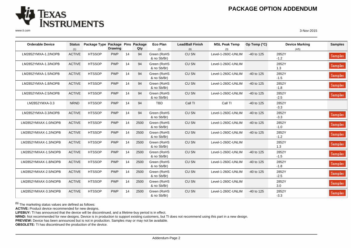
PACKAGING INFORMATION
Orderable Device Status(1)
Package Type PackageDrawing
Pins PackageQty
Eco Plan(2)
Lead/Ball Finish(6)
MSL Peak Temp(3)
Op Temp (°C) Device Marking(4/5)
Samples
LM2852XMXA-0.8/NOPB ACTIVE HTSSOP PWP 14 94 Green (RoHS& no Sb/Br)
CU SN Level-1-260C-UNLIM -40 to 125 2852X0.8
LM2852XMXA-1.0/NOPB ACTIVE HTSSOP PWP 14 94 Green (RoHS& no Sb/Br)
CU SN Level-1-260C-UNLIM -40 to 125 2852X1.0
LM2852XMXA-1.2 NRND HTSSOP PWP 14 TBD Call TI Call TI -40 to 125 2852X1.2
LM2852XMXA-1.2/NOPB ACTIVE HTSSOP PWP 14 94 Green (RoHS& no Sb/Br)
CU SN Level-1-260C-UNLIM -40 to 125 2852X1.2
LM2852XMXA-1.5 NRND HTSSOP PWP 14 TBD Call TI Call TI -40 to 125 2852X1.5
LM2852XMXA-1.5/NOPB ACTIVE HTSSOP PWP 14 94 Green (RoHS& no Sb/Br)
CU SN Level-1-260C-UNLIM -40 to 125 2852X1.5
LM2852XMXA-1.8/NOPB ACTIVE HTSSOP PWP 14 94 Green (RoHS& no Sb/Br)
CU SN Level-1-260C-UNLIM -40 to 125 2852X1.8
LM2852XMXA-2.5 NRND HTSSOP PWP 14 TBD Call TI Call TI -40 to 125 2852X2.5
LM2852XMXA-2.5/NOPB ACTIVE HTSSOP PWP 14 94 Green (RoHS& no Sb/Br)
CU SN Level-1-260C-UNLIM -40 to 125 2852X2.5
LM2852XMXA-3.0/NOPB ACTIVE HTSSOP PWP 14 94 Green (RoHS& no Sb/Br)
CU SN Level-1-260C-UNLIM 2852X3.0
LM2852XMXA-3.3/NOPB ACTIVE HTSSOP PWP 14 94 Green (RoHS& no Sb/Br)
CU SN Level-1-260C-UNLIM -40 to 125 2852X3.3
LM2852XMXAX-1.2/NOPB ACTIVE HTSSOP PWP 14 2500 Green (RoHS& no Sb/Br)
CU SN Level-1-260C-UNLIM -40 to 125 2852X1.2
LM2852XMXAX-1.5/NOPB ACTIVE HTSSOP PWP 14 2500 Green (RoHS& no Sb/Br)
CU SN Level-1-260C-UNLIM -40 to 125 2852X1.5
LM2852XMXAX-1.8/NOPB ACTIVE HTSSOP PWP 14 2500 Green (RoHS& no Sb/Br)
CU SN Level-1-260C-UNLIM -40 to 125 2852X1.8
LM2852XMXAX-2.5/NOPB ACTIVE HTSSOP PWP 14 2500 Green (RoHS& no Sb/Br)
CU SN Level-1-260C-UNLIM -40 to 125 2852X2.5
LM2852XMXAX-3.3/NOPB ACTIVE HTSSOP PWP 14 2500 Green (RoHS& no Sb/Br)
CU SN Level-1-260C-UNLIM -40 to 125 2852X3.3
LM2852YMXA-1.0/NOPB ACTIVE HTSSOP PWP 14 94 Green (RoHS& no Sb/Br)
CU SN Level-1-260C-UNLIM -40 to 125 2852Y-1.0
PACKAGE OPTION ADDENDUM
www.ti.com 3-Nov-2015
Addendum-Page 2
Orderable Device Status(1)
Package Type PackageDrawing
Pins PackageQty
Eco Plan(2)
Lead/Ball Finish(6)
MSL Peak Temp(3)
Op Temp (°C) Device Marking(4/5)
Samples
LM2852YMXA-1.2/NOPB ACTIVE HTSSOP PWP 14 94 Green (RoHS& no Sb/Br)
CU SN Level-1-260C-UNLIM -40 to 125 2852Y-1.2
LM2852YMXA-1.3/NOPB ACTIVE HTSSOP PWP 14 94 Green (RoHS& no Sb/Br)
CU SN Level-1-260C-UNLIM 2852Y1.3
LM2852YMXA-1.5/NOPB ACTIVE HTSSOP PWP 14 94 Green (RoHS& no Sb/Br)
CU SN Level-1-260C-UNLIM -40 to 125 2852Y-1.5
LM2852YMXA-1.8/NOPB ACTIVE HTSSOP PWP 14 94 Green (RoHS& no Sb/Br)
CU SN Level-1-260C-UNLIM -40 to 125 2852Y-1.8
LM2852YMXA-2.5/NOPB ACTIVE HTSSOP PWP 14 94 Green (RoHS& no Sb/Br)
CU SN Level-1-260C-UNLIM -40 to 125 2852Y-2.5
LM2852YMXA-3.3 NRND HTSSOP PWP 14 94 TBD Call TI Call TI -40 to 125 2852Y-3.3
LM2852YMXA-3.3/NOPB ACTIVE HTSSOP PWP 14 94 Green (RoHS& no Sb/Br)
CU SN Level-1-260C-UNLIM -40 to 125 2852Y-3.3
LM2852YMXAX-1.0/NOPB ACTIVE HTSSOP PWP 14 2500 Green (RoHS& no Sb/Br)
CU SN Level-1-260C-UNLIM -40 to 125 2852Y-1.0
LM2852YMXAX-1.2/NOPB ACTIVE HTSSOP PWP 14 2500 Green (RoHS& no Sb/Br)
CU SN Level-1-260C-UNLIM -40 to 125 2852Y-1.2
LM2852YMXAX-1.3/NOPB ACTIVE HTSSOP PWP 14 2500 Green (RoHS& no Sb/Br)
CU SN Level-1-260C-UNLIM 2852Y1.3
LM2852YMXAX-1.5/NOPB ACTIVE HTSSOP PWP 14 2500 Green (RoHS& no Sb/Br)
CU SN Level-1-260C-UNLIM -40 to 125 2852Y-1.5
LM2852YMXAX-1.8/NOPB ACTIVE HTSSOP PWP 14 2500 Green (RoHS& no Sb/Br)
CU SN Level-1-260C-UNLIM -40 to 125 2852Y-1.8
LM2852YMXAX-2.5/NOPB ACTIVE HTSSOP PWP 14 2500 Green (RoHS& no Sb/Br)
CU SN Level-1-260C-UNLIM -40 to 125 2852Y-2.5
LM2852YMXAX-3.0/NOPB ACTIVE HTSSOP PWP 14 2500 Green (RoHS& no Sb/Br)
CU SN Level-1-260C-UNLIM 2852Y3.0
LM2852YMXAX-3.3/NOPB ACTIVE HTSSOP PWP 14 2500 Green (RoHS& no Sb/Br)
CU SN Level-1-260C-UNLIM -40 to 125 2852Y-3.3
(1) The marketing status values are defined as follows:ACTIVE: Product device recommended for new designs.LIFEBUY: TI has announced that the device will be discontinued, and a lifetime-buy period is in effect.NRND: Not recommended for new designs. Device is in production to support existing customers, but TI does not recommend using this part in a new design.PREVIEW: Device has been announced but is not in production. Samples may or may not be available.OBSOLETE: TI has discontinued the production of the device.
PACKAGE OPTION ADDENDUM
www.ti.com 3-Nov-2015
Addendum-Page 3
(2) Eco Plan - The planned eco-friendly classification: Pb-Free (RoHS), Pb-Free (RoHS Exempt), or Green (RoHS & no Sb/Br) - please check http://www.ti.com/productcontent for the latest availabilityinformation and additional product content details.TBD: The Pb-Free/Green conversion plan has not been defined.Pb-Free (RoHS): TI's terms "Lead-Free" or "Pb-Free" mean semiconductor products that are compatible with the current RoHS requirements for all 6 substances, including the requirement thatlead not exceed 0.1% by weight in homogeneous materials. Where designed to be soldered at high temperatures, TI Pb-Free products are suitable for use in specified lead-free processes.Pb-Free (RoHS Exempt): This component has a RoHS exemption for either 1) lead-based flip-chip solder bumps used between the die and package, or 2) lead-based die adhesive used betweenthe die and leadframe. The component is otherwise considered Pb-Free (RoHS compatible) as defined above.Green (RoHS & no Sb/Br): TI defines "Green" to mean Pb-Free (RoHS compatible), and free of Bromine (Br) and Antimony (Sb) based flame retardants (Br or Sb do not exceed 0.1% by weightin homogeneous material)
(3) MSL, Peak Temp. - The Moisture Sensitivity Level rating according to the JEDEC industry standard classifications, and peak solder temperature.
(4) There may be additional marking, which relates to the logo, the lot trace code information, or the environmental category on the device.
(5) Multiple Device Markings will be inside parentheses. Only one Device Marking contained in parentheses and separated by a "~" will appear on a device. If a line is indented then it is a continuationof the previous line and the two combined represent the entire Device Marking for that device.
(6) Lead/Ball Finish - Orderable Devices may have multiple material finish options. Finish options are separated by a vertical ruled line. Lead/Ball Finish values may wrap to two lines if the finishvalue exceeds the maximum column width.
Important Information and Disclaimer:The information provided on this page represents TI's knowledge and belief as of the date that it is provided. TI bases its knowledge and belief on informationprovided by third parties, and makes no representation or warranty as to the accuracy of such information. Efforts are underway to better integrate information from third parties. TI has taken andcontinues to take reasonable steps to provide representative and accurate information but may not have conducted destructive testing or chemical analysis on incoming materials and chemicals.TI and TI suppliers consider certain information to be proprietary, and thus CAS numbers and other limited information may not be available for release.
In no event shall TI's liability arising out of such information exceed the total purchase price of the TI part(s) at issue in this document sold by TI to Customer on an annual basis.
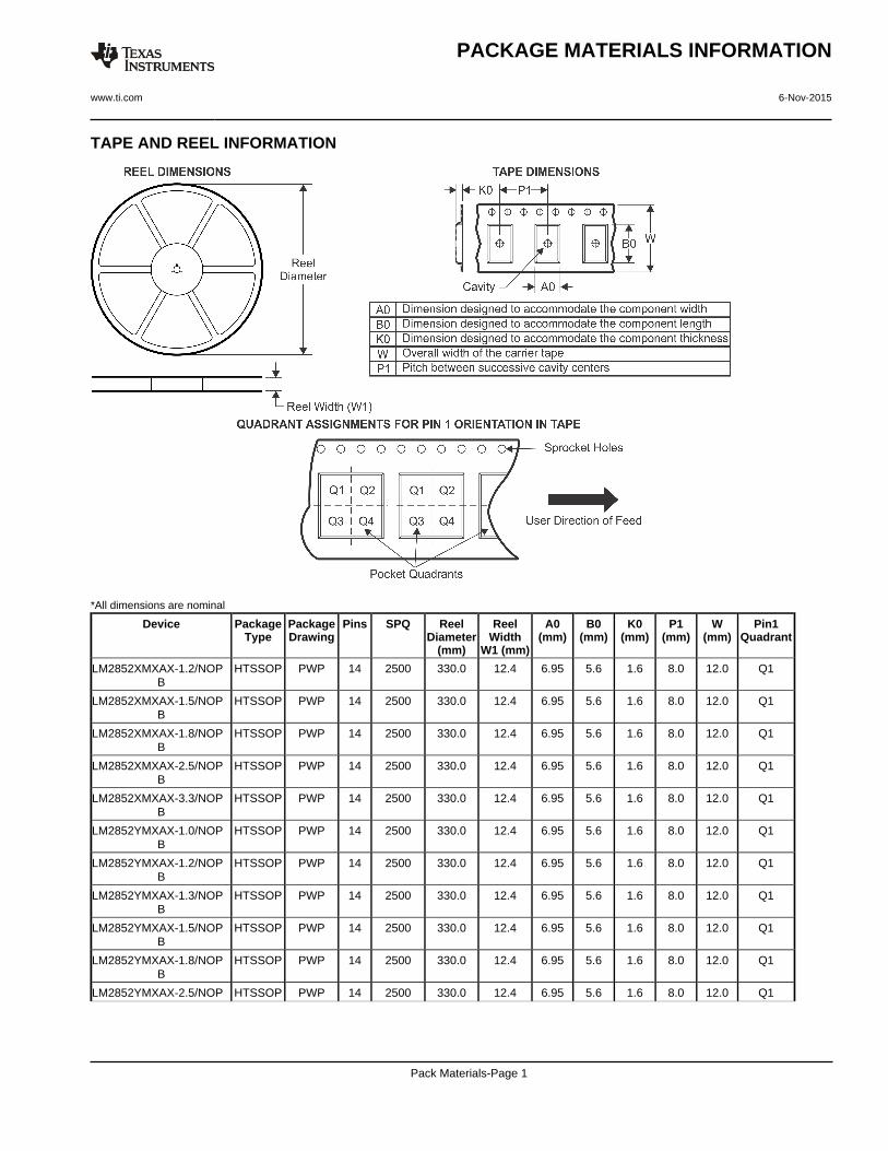
TAPE AND REEL INFORMATION
*All dimensions are nominal
Device PackageType
PackageDrawing
Pins SPQ ReelDiameter
(mm)
ReelWidth
W1 (mm)
A0(mm)
B0(mm)
K0(mm)
P1(mm)
W(mm)
Pin1Quadrant
LM2852XMXAX-1.2/NOPB
HTSSOP PWP 14 2500 330.0 12.4 6.95 5.6 1.6 8.0 12.0 Q1
LM2852XMXAX-1.5/NOPB
HTSSOP PWP 14 2500 330.0 12.4 6.95 5.6 1.6 8.0 12.0 Q1
LM2852XMXAX-1.8/NOPB
HTSSOP PWP 14 2500 330.0 12.4 6.95 5.6 1.6 8.0 12.0 Q1
LM2852XMXAX-2.5/NOPB
HTSSOP PWP 14 2500 330.0 12.4 6.95 5.6 1.6 8.0 12.0 Q1
LM2852XMXAX-3.3/NOPB
HTSSOP PWP 14 2500 330.0 12.4 6.95 5.6 1.6 8.0 12.0 Q1
LM2852YMXAX-1.0/NOPB
HTSSOP PWP 14 2500 330.0 12.4 6.95 5.6 1.6 8.0 12.0 Q1
LM2852YMXAX-1.2/NOPB
HTSSOP PWP 14 2500 330.0 12.4 6.95 5.6 1.6 8.0 12.0 Q1
LM2852YMXAX-1.3/NOPB
HTSSOP PWP 14 2500 330.0 12.4 6.95 5.6 1.6 8.0 12.0 Q1
LM2852YMXAX-1.5/NOPB
HTSSOP PWP 14 2500 330.0 12.4 6.95 5.6 1.6 8.0 12.0 Q1
LM2852YMXAX-1.8/NOPB
HTSSOP PWP 14 2500 330.0 12.4 6.95 5.6 1.6 8.0 12.0 Q1
LM2852YMXAX-2.5/NOP HTSSOP PWP 14 2500 330.0 12.4 6.95 5.6 1.6 8.0 12.0 Q1
PACKAGE MATERIALS INFORMATION
www.ti.com 6-Nov-2015
Pack Materials-Page 1
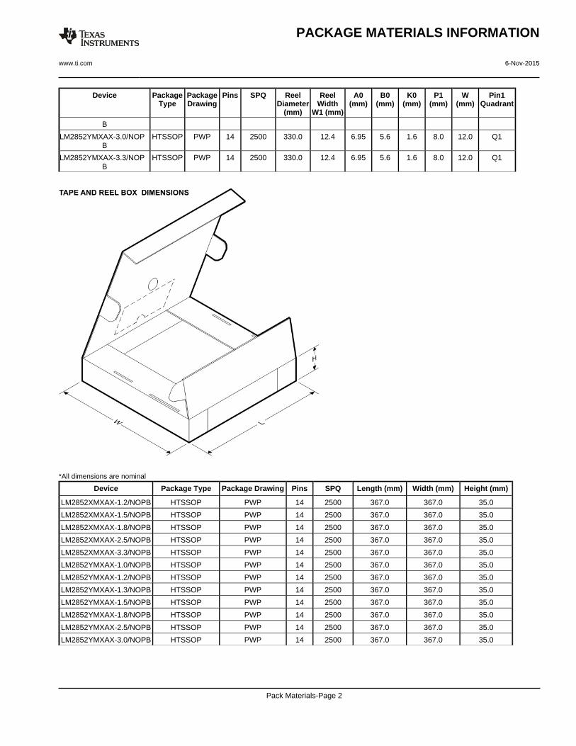
Device PackageType
PackageDrawing
Pins SPQ ReelDiameter
(mm)
ReelWidth
W1 (mm)
A0(mm)
B0(mm)
K0(mm)
P1(mm)
W(mm)
Pin1Quadrant
B
LM2852YMXAX-3.0/NOPB
HTSSOP PWP 14 2500 330.0 12.4 6.95 5.6 1.6 8.0 12.0 Q1
LM2852YMXAX-3.3/NOPB
HTSSOP PWP 14 2500 330.0 12.4 6.95 5.6 1.6 8.0 12.0 Q1
*All dimensions are nominal
Device Package Type Package Drawing Pins SPQ Length (mm) Width (mm) Height (mm)
LM2852XMXAX-1.2/NOPB HTSSOP PWP 14 2500 367.0 367.0 35.0
LM2852XMXAX-1.5/NOPB HTSSOP PWP 14 2500 367.0 367.0 35.0
LM2852XMXAX-1.8/NOPB HTSSOP PWP 14 2500 367.0 367.0 35.0
LM2852XMXAX-2.5/NOPB HTSSOP PWP 14 2500 367.0 367.0 35.0
LM2852XMXAX-3.3/NOPB HTSSOP PWP 14 2500 367.0 367.0 35.0
LM2852YMXAX-1.0/NOPB HTSSOP PWP 14 2500 367.0 367.0 35.0
LM2852YMXAX-1.2/NOPB HTSSOP PWP 14 2500 367.0 367.0 35.0
LM2852YMXAX-1.3/NOPB HTSSOP PWP 14 2500 367.0 367.0 35.0
LM2852YMXAX-1.5/NOPB HTSSOP PWP 14 2500 367.0 367.0 35.0
LM2852YMXAX-1.8/NOPB HTSSOP PWP 14 2500 367.0 367.0 35.0
LM2852YMXAX-2.5/NOPB HTSSOP PWP 14 2500 367.0 367.0 35.0
LM2852YMXAX-3.0/NOPB HTSSOP PWP 14 2500 367.0 367.0 35.0
PACKAGE MATERIALS INFORMATION
www.ti.com 6-Nov-2015
Pack Materials-Page 2

Device Package Type Package Drawing Pins SPQ Length (mm) Width (mm) Height (mm)
LM2852YMXAX-3.3/NOPB HTSSOP PWP 14 2500 367.0 367.0 35.0
PACKAGE MATERIALS INFORMATION
www.ti.com 6-Nov-2015
Pack Materials-Page 3
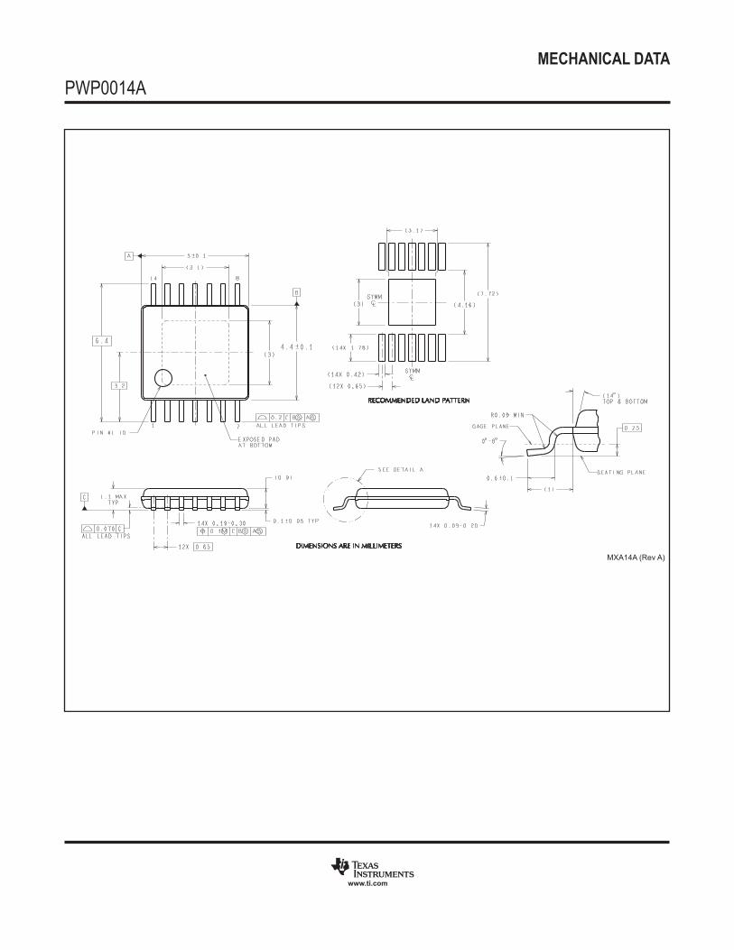
MECHANICAL DATA
PWP0014A
www.ti.com
MXA14A (Rev A)
IMPORTANT NOTICE
Texas Instruments Incorporated and its subsidiaries (TI) reserve the right to make corrections, enhancements, improvements and otherchanges to its semiconductor products and services per JESD46, latest issue, and to discontinue any product or service per JESD48, latestissue. Buyers should obtain the latest relevant information before placing orders and should verify that such information is current andcomplete. All semiconductor products (also referred to herein as “components”) are sold subject to TI’s terms and conditions of salesupplied at the time of order acknowledgment.TI warrants performance of its components to the specifications applicable at the time of sale, in accordance with the warranty in TI’s termsand conditions of sale of semiconductor products. Testing and other quality control techniques are used to the extent TI deems necessaryto support this warranty. Except where mandated by applicable law, testing of all parameters of each component is not necessarilyperformed.TI assumes no liability for applications assistance or the design of Buyers’ products. Buyers are responsible for their products andapplications using TI components. To minimize the risks associated with Buyers’ products and applications, Buyers should provideadequate design and operating safeguards.TI does not warrant or represent that any license, either express or implied, is granted under any patent right, copyright, mask work right, orother intellectual property right relating to any combination, machine, or process in which TI components or services are used. Informationpublished by TI regarding third-party products or services does not constitute a license to use such products or services or a warranty orendorsement thereof. Use of such information may require a license from a third party under the patents or other intellectual property of thethird party, or a license from TI under the patents or other intellectual property of TI.Reproduction of significant portions of TI information in TI data books or data sheets is permissible only if reproduction is without alterationand is accompanied by all associated warranties, conditions, limitations, and notices. TI is not responsible or liable for such altereddocumentation. Information of third parties may be subject to additional restrictions.Resale of TI components or services with statements different from or beyond the parameters stated by TI for that component or servicevoids all express and any implied warranties for the associated TI component or service and is an unfair and deceptive business practice.TI is not responsible or liable for any such statements.Buyer acknowledges and agrees that it is solely responsible for compliance with all legal, regulatory and safety-related requirementsconcerning its products, and any use of TI components in its applications, notwithstanding any applications-related information or supportthat may be provided by TI. Buyer represents and agrees that it has all the necessary expertise to create and implement safeguards whichanticipate dangerous consequences of failures, monitor failures and their consequences, lessen the likelihood of failures that might causeharm and take appropriate remedial actions. Buyer will fully indemnify TI and its representatives against any damages arising out of the useof any TI components in safety-critical applications.In some cases, TI components may be promoted specifically to facilitate safety-related applications. With such components, TI’s goal is tohelp enable customers to design and create their own end-product solutions that meet applicable functional safety standards andrequirements. Nonetheless, such components are subject to these terms.No TI components are authorized for use in FDA Class III (or similar life-critical medical equipment) unless authorized officers of the partieshave executed a special agreement specifically governing such use.Only those TI components which TI has specifically designated as military grade or “enhanced plastic” are designed and intended for use inmilitary/aerospace applications or environments. Buyer acknowledges and agrees that any military or aerospace use of TI componentswhich have not been so designated is solely at the Buyer's risk, and that Buyer is solely responsible for compliance with all legal andregulatory requirements in connection with such use.TI has specifically designated certain components as meeting ISO/TS16949 requirements, mainly for automotive use. In any case of use ofnon-designated products, TI will not be responsible for any failure to meet ISO/TS16949.
Products ApplicationsAudio www.ti.com/audio Automotive and Transportation www.ti.com/automotiveAmplifiers amplifier.ti.com Communications and Telecom www.ti.com/communicationsData Converters dataconverter.ti.com Computers and Peripherals www.ti.com/computersDLP® Products www.dlp.com Consumer Electronics www.ti.com/consumer-appsDSP dsp.ti.com Energy and Lighting www.ti.com/energyClocks and Timers www.ti.com/clocks Industrial www.ti.com/industrialInterface interface.ti.com Medical www.ti.com/medicalLogic logic.ti.com Security www.ti.com/securityPower Mgmt power.ti.com Space, Avionics and Defense www.ti.com/space-avionics-defenseMicrocontrollers microcontroller.ti.com Video and Imaging www.ti.com/videoRFID www.ti-rfid.comOMAP Applications Processors www.ti.com/omap TI E2E Community e2e.ti.comWireless Connectivity www.ti.com/wirelessconnectivity
Mailing Address: Texas Instruments, Post Office Box 655303, Dallas, Texas 75265Copyright © 2016, Texas Instruments Incorporated


![g]kfnL nf sjftf] tyf nf{ ]shLjg](https://img.pdfslide.net/doc/110x75/62091bd4c59e5d1fdc43555b/gkfnl-nf-sjftf-tyf-nf-shljg.jpg)