Embed Size (px)
Citation preview

LM3311
www.ti.com SNVS320G –AUGUST 2005–REVISED APRIL 2013
LM3311 Step-Up PWM DC/DC Converter with Integrated LDO, Op-Amp, and Gate PulseModulation SwitchCheck for Samples: LM3311
1FEATURES DESCRIPTIONThe LM3311 is a step-up DC/DC converter integrated
2• Boost Converter with a 2A, 0.18Ω Switchwith an LDO, an Operational Amplifier, and a gate
• Boost Output Voltage Adjustable up to 20V pulse modulation switch. The boost (step-up)• Operating Voltage Range of 2.5V to 7V converter is used to generate an adjustable output
voltage and features a low RDSON internal switch for• 660kHz/1.28MHz Pin Selectable Switchingmaximum efficiency. The operating frequency isFrequencyselectable between 660kHz and 1.28MHz allowing for
• Adjustable Soft-Start Function the use of small external components. An external• Input Undervoltage Protection soft-start pin enables the user to tailor the soft-start
time to a specific application and limit the inrush• Over Temperature Protectioncurrent. The LDO also has an adjustable output• Adjustable Low Dropout Linear Regulator voltage and is stable using ceramic output capacitors.
(LDO) The Op-Amp is capable of sourcing/sinking 135mA of• Integrated Op-Amp current (typical) for the standard version and 200mA
(typical) for the HIOP version. The gate pulse• Integrated Gate Pulse Modulation (GPM)modulation switch can operate with a VGH voltage ofSwitch5V to 30V. The LM3311 is available in a low profile
• 24-Lead WQFN Package 24-lead WQFN package.
APPLICATIONS• TFT Bias Supplies• Portable Applications
1
Please be aware that an important notice concerning availability, standard warranty, and use in critical applications ofTexas Instruments semiconductor products and disclaimers thereto appears at the end of this data sheet.
2All trademarks are the property of their respective owners.
PRODUCTION DATA information is current as of publication date. Copyright © 2005–2013, Texas Instruments IncorporatedProducts conform to specifications per the terms of the TexasInstruments standard warranty. Production processing does notnecessarily include testing of all parameters.

NC
VGHM
VFLK
NE
G
VDPM
PO
S
AG
ND
VDD
AD
J
AVIN
OU
T
SW
VIN
VC
121110987
13
14
18
17
16
15
1
2
3
4
5
6
21222324
LVIN
SS
VO
UT
FREQLM3311
1920
PG
ND
RE
CE
VG
H
SH
DN
FB
VDD
LVIN
CSS
VOUT
CIN
COUT
VIN
FB
SW
ADJ
SS
AGNDVOUT
POS
NEG
SHDN FREQ
LM3311
VC
D3D2
C2 C1
D1L
RFB1
RFB2
VIN
CC
RC
PGND
OUT
VDPM
VGHM
VFLK
CERE
VGH
RE CE
= 2 X
LDO Output
LDO Input
AVIN
RADJ1
RADJ2
C3 C4
R1
R2
VOUT
VOH
LM3311
SNVS320G –AUGUST 2005–REVISED APRIL 2013 www.ti.com
Typical Application Circuit
Connection Diagram
Figure 1. 24-Lead WQFN (Top View)See RTW0024A Package
θJA=37°C/W
Pin DescriptionsPin Name Function
1 NC Not internally connected.
2 Submit Documentation Feedback Copyright © 2005–2013, Texas Instruments Incorporated
Product Folder Links: LM3311

LM3311
www.ti.com SNVS320G –AUGUST 2005–REVISED APRIL 2013
Pin Descriptions (continued)
Pin Name Function
2 VGHM Output of GPM circuit. This output directly drives the supply for the gate driver circuits.
3 VFLK Determines when the TFT LCD is on or off. This is controlled by the timing controller in the LCDmodule.
4 VDPM VDPM pin is the enable signal for the GPM block. Pulling this pin high enables the GPM whilepulling this pin low disables it. VDPM is used for timing sequence control.
5 VDD Reference input for gate pulse modulation (GPM) circuit. The voltage at VDD is used to set the lowerVGHM voltage. If the GPM function is not used connect VDD to VIN.
6 AVIN Op-Amp analog power input.
7 OUT Output of the Op-Amp.
8 NEG Negative input terminal of the Op-Amp.
9 POS Positive input terminal of the Op-Amp.
10 AGND Analog ground for the step-up regulator, LDO, and Op-Amp. Connect directly to DAP and PGNDbeneath the device.
11 ADJ LDO output voltage feedback input.
12 VOUT LDO regulator output.
13 LVIN LDO power input.
14 SS Boost converter soft start pin.
15 VC Boost compensation network connection. Connected to the output of the voltage error amplifier.
16 FREQ Switching frequency select input. Connect this pin to VIN for 1.28MHz operation and AGND for660kHz operation.
17 VIN Boost converter and GPM power input.
18 SW Boost power switch input. Switch connected between SW pin and PGND pin.
19 SHDN Shutdown pin. Active low, pulling this pin low will disable the LM3311.
20 FB Boost output voltage feedback input.
21 PGND Power Ground. Source connection of the step-up regulator NMOS switch and ground for the GPMcircuit. Connect AGND and PGND directly to the DAP beneath the device.
22 CE Connect capacitor from this pin to AGND.
23 RE Connect a resistor between RE and PGND.
24 VGH GPM power supply input. VGH range is 5V to 30V.
DAP Die Attach Pad. Internally connected to GND. Connect AGND and PGND pins directly to this padbeneath the device.
Copyright © 2005–2013, Texas Instruments Incorporated Submit Documentation Feedback 3
Product Folder Links: LM3311

Boost Converter
+
-
+
-
+
-
+
- R
SQ
Current
Sense
osc
+
-
Softstart
Bandgap
+
-
BG
REF
D REF
VIN
BG
T REF
BG
PWM
Comp
EAMP
LLcomp
Dcomp
Driver
N1UVP
Comp
TSD
Comp
Reset
UVPREF
20
15
21
18
19
350 k:
17
V IN
16
14
PGND
10
AGND
AGND PGND
SHDN
FB
VC
V IN FREQ
SW
SSISS
VIN
LM3311
SNVS320G –AUGUST 2005–REVISED APRIL 2013 www.ti.com
Block Diagrams
Figure 2.
4 Submit Documentation Feedback Copyright © 2005–2013, Texas Instruments Incorporated
Product Folder Links: LM3311

+
-
xBG
+
-Reset
BG
AGND
AGND
PGND
10
AGND
AGND 21
PGND
PGND
24
2
23
4
22
3
5
VDD
VGH
VGHM
RE
VDPM
CE
VFLK
PGND
PGND
350 k:
350 k:
1 k:
9R
R
AGND
CE
P2
P3
N2
N3
AGND
2x or 3x Charge
Pump
PGND
R1
R2
RE
VIN
ICE
GPM Block
LM3311
www.ti.com SNVS320G –AUGUST 2005–REVISED APRIL 2013
Figure 3.
Copyright © 2005–2013, Texas Instruments Incorporated Submit Documentation Feedback 5
Product Folder Links: LM3311

+
-
10AGND
7
6
9
8
OUTPOS
NEG
AVIN
Reset
Op-Amp
+
-
+
-
13
12
11
BG
Reset
SS
10
AGND
AGND
0.84V
Input
Amplifier
Short Circuit
CompADJ
LVIN
VOUTP1
LDO
LM3311
SNVS320G –AUGUST 2005–REVISED APRIL 2013 www.ti.com
Figure 4.
Figure 5.
These devices have limited built-in ESD protection. The leads should be shorted together or the device placed in conductive foamduring storage or handling to prevent electrostatic damage to the MOS gates.
6 Submit Documentation Feedback Copyright © 2005–2013, Texas Instruments Incorporated
Product Folder Links: LM3311

LM3311
www.ti.com SNVS320G –AUGUST 2005–REVISED APRIL 2013
Absolute Maximum Ratings (1) (2)
VIN 7.5V
SW Voltage 21V
FB Voltage VIN
VC Voltage (3) 1.265V ± 0.3V
SHDN Voltage 7.5V
FREQ VIN
AVIN 14.5V
Amplifier Inputs/Output Rail-to-Rail
LVIN 7.5V
ADJ Voltage LVIN
VOUT LVIN
VGH Voltage 31V
VGHM Voltage VGH
VFLK, VDPM, VDD Voltage 7.5V
CE Voltage (3) 1.265 + 0.3V
RE Voltage VGH
Maximum Junction Temperature 150°C
Power Dissipation (4) Internally Limited
Lead Temperature 300°C
Vapor Phase (60 sec.) 215°C
Infrared (15 sec.) 220°C
ESD Susceptibility (5)
Human Body Model 2kV
(1) Absolute maximum ratings are limits beyond which damage to the device may occur. Operating Ratings are conditions for which thedevice is intended to be functional, but device parameter specifications may not be ensured. For ensured specifications and testconditions, see the Electrical Characteristics.
(2) If Military/Aerospace specified devices are required, please contact the Texas Instruments Sales Office/ Distributors for availability andspecifications.
(3) Under normal operation the VC and CE pins may go to voltages above this value. The maximum rating is for the possibility of a voltagebeing applied to the pin, however the VC and CE pins should never have a voltage directly applied to them.
(4) The maximum allowable power dissipation is a function of the maximum junction temperature, TJ(MAX), the junction-to-ambient thermalresistance, θJA, and the ambient temperature, TA. See the Electrical Characteristics table for the thermal resistance of various layouts.The maximum allowable power dissipation at any ambient temperature is calculated using: PD (MAX) = (TJ(MAX) − TA)/θJA. Exceedingthe maximum allowable power dissipation will cause excessive die temperature, and the regulator will go into thermal shutdown.
(5) The human body model is a 100pF capacitor discharged through a 1.5kΩ resistor into each pin per JEDEC standard JESD22-A114.
Operating ConditionsOperating Junction Temperature Range (1) −40°C to +125°C
Storage Temperature −65°C to +150°C
Supply Voltage 2.5V to 7V
Maximum SW Voltage 20V
VGH Voltage Range 5V to 30V
Op-Amp Supply, AVIN 4V to 14V
LDO Supply, LVIN 2.5V to 7V
(1) All limits specified at room temperature (standard typeface) and at temperature extremes (bold typeface). All room temperature limits are100% production tested. All limits at temperature extremes are specified via correlation using standard Statistical Quality Control (SQC)methods. All limits are used to calculate Average Outgoing Quality Level (AOQL).
Copyright © 2005–2013, Texas Instruments Incorporated Submit Documentation Feedback 7
Product Folder Links: LM3311

LM3311
SNVS320G –AUGUST 2005–REVISED APRIL 2013 www.ti.com
Electrical CharacteristicsSpecifications in standard type face are for TJ = 25°C and those with boldface type apply over the full OperatingTemperature Range ( TJ = −40°C to +125°C). Unless otherwise specified, VIN = LVIN = 2.5V and IL = 0A.
Min Typ MaxSymbol Parameter Conditions Units(1) (2) (1)
IQ Quiescent Current FB = 2V (Not Switching) 690 1100µAVSHDN = 0V 0.50.04 8.5
660kHz Switching 2.1 2.8mA
1.28MHz Switching 3.1 4.0
VFB Feedback Voltage 1.231 1.263 1.287 V
%VFB/ΔVIN Feedback Voltage Line 2.5V ≤ VIN ≤ 7V -0.26 0.089 0.42 %/VRegulation
ICL Switch Current Limit (3) (4) 2.0 2.6 A
IB FB Pin Bias Current (5) 27 160 nA
ISS SS Pin Current 8.5 11 13.5 µA
VSS SS Pin Voltage 1.20 1.24 1.28 V
VIN Input Voltage Range 2.5 7 V
gm Error Amp Transconductance ΔI = 5µA 26 74 133 µmho
AV Error Amp Voltage Gain 69 V/V
DMAX Maximum Duty Cycle fS = 660kHz 80 91%
fS = 1.28MHz 80 89
fS Switching Frequency FREQ = Ground 440 660 760 kHz
FREQ = VIN 1.0 1.28 1.5 MHz
ISHDN Shutdown Pin Current VSHDN = 2.5V 8 13.5 µA
VSHDN = 0.3V 1 2
IL Switch Leakage Current VSW = 20V 0.03 5 µA
RDSON Switch RDSON ISW = 500mA 0.18 0.35 ΩThSHDN SHDN Threshold Output High, VIN = 2.5V to 7V 1.4 V
Output Low, VIN = 2.5V to 7V 0.4
UVP Undervoltage Protection On Threshold (Switch On) 2.5 2.4VThreshold Off Threshold (Switch Off) 2.3 2.1
IFREQ FREQ Pin Current FREQ = VIN = 2.5V 2.7 13.5 µA
Operational Amplifier
VOS Input Offset Voltage Buffer configuration, VO = 5.7 15AVIN/2, no loadmV
Buffer configuration, VO = 5.7 16AVIN/2, no load (HIOP version)
IB Input Bias Current (POS Pin) Buffer configuration, VO = 200 550 nAAVIN/2, no load (5)
VOUT Swing Buffer, RL=2kΩ, VO min. 0.001 0.03V
Buffer, RL=2kΩ, VO max. 7.9 7.97
AVIN Supply Voltage 4 14 V
Is+ Supply Current Buffer, VO = AVIN/2, No Load 1.5 7.8mABuffer, VO = AVIN/2, No Load 2.5 9(HIOP version)
(1) All limits specified at room temperature (standard typeface) and at temperature extremes (bold typeface). All room temperature limits are100% production tested. All limits at temperature extremes are specified via correlation using standard Statistical Quality Control (SQC)methods. All limits are used to calculate Average Outgoing Quality Level (AOQL).
(2) Typical numbers are at 25°C and represent the most likely norm.(3) Duty cycle affects current limit due to ramp generator.(4) Current limit at 0% duty cycle. See Typical Performance Characteristics section for Switch Current Limit vs. VIN(5) Bias current flows into pin.
8 Submit Documentation Feedback Copyright © 2005–2013, Texas Instruments Incorporated
Product Folder Links: LM3311

LM3311
www.ti.com SNVS320G –AUGUST 2005–REVISED APRIL 2013
Electrical Characteristics (continued)Specifications in standard type face are for TJ = 25°C and those with boldface type apply over the full OperatingTemperature Range ( TJ = −40°C to +125°C). Unless otherwise specified, VIN = LVIN = 2.5V and IL = 0A.
Min Typ MaxSymbol Parameter Conditions Units(1) (2) (1)
IOUT Output Current Source 90 138 195
Sink 105 135 175mA
Source (HIOP version) 140 215 270
Sink (HIOP version) 175 205 260
SR Slew Rate CL = 10pF (6) 50 V/µs
GBW Gain Bandwidth -3dB, CL = 100pF 3.3 MHz
Gate Pulse Modulation
VFLK VFLK Voltage Levels Rising edge threshold 1.4V
Falling edge threshold 0.4
VDPM VDPM Voltage Levels Rising edge threshold 1.4V
Falling edge threshold 0.4
VDD(TH) VDD Threshold VGHM = 30V 2.8 3 3.3V
VGHM = 5V 0.4 0.5 0.7
IVFLK VFLK Current VFLK = 1.5V 4.8 11µA
VFLK = 0.3V 1.1 2.5
IVDPM VDPM Current VDPM = 1.5V 4.8 11µA
VDPM = 0.3V 1.1 2.5
IVGH VGH Bias Current VGH = 30V, VFLK High 59 300µA
VGH = 30V, VFLK Low 11 35.5
RVGH-VGHM VGH to VGHM Resistance 20mA Current, VGH = 30V 14 28.5ΩRVGHM-RE VGHM to RE Resistance 20mA Current, VGH = VGHM 27 55= 30V
RVGHM(OFF) VGH Resistance VDPM is Low, VGHM = 2V 1.2 1.7 kΩICE CE Current CE = 0V 40 57 71 µA
VCE(TH) CE Voltage Threshold 1.16 1.22 1.30 V
Low Dropout Linear Regulator (LDO)
LVIN Input Voltage Range 2.5 7 V
VADJ ADJ Pin Voltage LVIN = 3V and 7V 1.197 1.263 1.289 V
IADJ ADJ Pin Current (7) 28 380 nA
%VADJ/ΔVIN ADJ Voltage Line Regulation LVIN = 3V to 7V, LDOOUT = -2.6 0.032 1.4 %2.8V, no load
%VADJ/ΔIL LDOOUT Load Regulation IOUT = 10mA to 300mA, LVIN = -11.6 2.931 8 %3.3V, LDOOUT = 2.8V
IQL LVIN Quiescent Current Device enabled 290 425µA
Device shut down 10.5
VDO Dropout Voltage 350mA load, LDOOUT = 2.8V 218 409 674 mV
VADJ(LOW) VADJ Short Circuit Disable LVIN = 3.3V 0.85 0.9 VThreshold
(6) Input signal is overdriven to force the output to swing rail to rail.(7) Bias current flows into pin.
Copyright © 2005–2013, Texas Instruments Incorporated Submit Documentation Feedback 9
Product Folder Links: LM3311

2.5 3.0 3.5 4.0 4.5 5.0 5.5 6.0 6.5 7.0
INPUT VOLTAGE (V)
CE
PIN
CU
RR
EN
T (P
A)
50.4
52.4
54.4
56.4
58.4
60.4
62.4
64.4
66.4
J= 125°CT
J= 25°CT
J= -40°CT
VDPM PIN VOLTAGE (V)
0
5
10
15
20
25
VD
PM
PIN
CU
RR
EN
T (P
A)
0.5 1.5 2.5 3.5 4.5 5.5 6.50.0 1.0 2.0 3.0 4.0 5.0 6.0 7.0
TJ = 25°C
JT = -40°C
JT = 125°C
FB = 1.265V
0
10
20
30
40
50
60
-40 -25 -10 5 20 35 50 65 80 95 110 125
JUNCTION TEMPERATURE (°C)
V = 7.0VIN
V = 2.5VIN
FB
PIN
CU
RR
EN
T (
nA)
2.5 3.0 3.5 4.0 4.5 5.0 5.5 6.0 6.5 7.0
INPUT VOLTAGE (V)
FR
EQ
PIN
CU
RR
EN
T (P
A)
TJ = 25°C
1.5
2.0
2.5
3.0
3.5
4.0
4.5
6.5
7.0
TJ = 125°C
TJ = -40°C
5.0
5.5
6.0
SHDN PIN VOLTAGE (V)
0
5
10
15
20
30
SH
DN
PIN
CU
RR
EN
T (P
A)
0.5 1.5 2.5 3.5 4.5 5.5 6.50.0 1.0 2.0 3.0 4.0 5.0 6.0 7.0
TJ = 25°C
JT = -40°C
T = 125°CJ
25
2.5 3.0 3.5 4.0 4.5 5.0 5.5 6.0 6.5 7.0
INPUT VOLTAGE (V)
TJ = 25°C
TJ = -40°C
TJ = 125°C
SS
PIN
CU
RR
EN
T (P
A)
10.4
10.6
10.8
11.0
11.2
11.4
11.6
11.8
12.0
LM3311
SNVS320G –AUGUST 2005–REVISED APRIL 2013 www.ti.com
Typical Performance Characteristics
SHDN Pin Current SS Pin Currentvs. vs.
SHDN Pin Voltage Input Voltage
Figure 6. Figure 7.
FREQ Pin Current FB Pin Currentvs. vs.
Input Voltage Temperature
Figure 8. Figure 9.
CE Pin Current VDPM Pin Currentvs. vs.
Input Voltage VDPM Pin Voltage
Figure 10. Figure 11.
10 Submit Documentation Feedback Copyright © 2005–2013, Texas Instruments Incorporated
Product Folder Links: LM3311

-25 -10 5 20 35 50 65 80 95 110125
JUNCTION TEMPERATURE (oC)
550
560
570
580
590
600
610
SW
ITC
HIN
G F
RE
QU
EN
CY
(kH
z)
-40
VIN = 2.5V
VIN = 7.0V
2.8
3.2
3.6
4.0
4.4
4.8
5.2
5.6
6.0
6.4
6.8
-40 -25 -10 5 20 35 50 65 80 95 110 125
JUNCTION TEMPERATURE (°C)
SW
ITC
HIN
G I Q
(m
A)
V = 2.5VIN
V = 7.0VIN
-25 -10 5 20 35 50 65 80 95 110125
JUNCTION TEMPERATURE (oC)
1.8
2.2
2.6
3.0
3.4
3.8
4.2
SW
ITC
HIN
G I Q
(m
A)
-40
VIN = 2.5V
2.0
2.4
2.8
3.2
3.6
4.0 VIN = 7.0V
2.5 3.0 3.5 4.0 4.5 5.0 5.5 6.0 6.5 7.0
INPUT VOLTAGE (V)
SW
ITC
HIN
G I Q
(m
A)
TJ = 25°C
2.75
3.25
3.75
4.25
4.75
5.25
5.75
6.25
6.75
TJ = -40°C
TJ = 125°C
2.5 7.01.8
2.0
2.4
2.8
3.0
3.2
3.6
3.8
4.0
SW
ITC
HIN
G I Q
(m
A)
INPUT VOLTAGE (V)
2.2
3.0 3.5 4.0 4.5 5.0 5.5 6.0 6.5
3.4
2.6TJ = 125oC
TJ = -40oC
TJ = 25oC
VFLK PIN VOLTAGE (V)
0
5
10
15
20
25
VF
LK P
IN C
UR
RE
NT
(P
A)
0.5 1.5 2.5 3.5 4.5 5.5 6.50.0 1.0 2.0 3.0 4.0 5.0 6.0 7.0
TJ = 25°C
JT = -40°C
JT = 125°C
LM3311
www.ti.com SNVS320G –AUGUST 2005–REVISED APRIL 2013
Typical Performance Characteristics (continued)VFLK Pin Current 660kHz Switching Quiescent Current
vs. vs.VFLK Pin Voltage Input Voltage
Figure 12. Figure 13.
1.28MHz Switching Quiescent Current 660kHz Switching Quiescent Currentvs. vs.
Input Voltage Temperature
Figure 14. Figure 15.
1.28MHz Switching Quiescent Current 660kHz Switching Frequencyvs. vs.
Temperature Temperature
Figure 16. Figure 17.
Copyright © 2005–2013, Texas Instruments Incorporated Submit Documentation Feedback 11
Product Folder Links: LM3311

JUNCTION TEMPERATURE (°C)
NO
N-S
WIT
CH
ING
I Q (
mA
)
0.66
0.69
0.72
0.75
0.78
0.81
0.84
-40 -25 -10 5 20 35 50 65 80 95 110 125
VIN = 7.0V
VIN = 2.5V
GPM Disabled
JUNCTION TEMPERATURE (°C)
NO
N-S
WIT
CH
ING
I Q (
mA
)
0.93
0.99
1.02
1.08
1.14
1.23
-40 -25 -10 5 20 35 50 65 80 95 110 125
GPM Enabled
VIN = 7.0V
VIN = 2.5V
0.96
1.05
1.11
1.17
1.20
2.5 3.0 3.5 4.0 4.5 5.0 5.5 6.0 6.5 7.0
INPUT VOLTAGE (V)
NO
N-S
WIT
CH
ING
I Q (
mA
)
0.66
0.69
0.72
0.75
0.78
0.81
0.84
J= -40°CT
J= 25°CT
J= 125°CT
GPM Disabled
2.5 3.0 3.5 4.0 4.5 5.0 5.5 6.0 6.5 7.0
INPUT VOLTAGE (V)
NO
N-S
WIT
CH
ING
I Q (
mA
)
0.93
0.96
1.02
1.05
1.11
1.14
1.20
J= 125°CT
J= 25°CT
J= -40°CT
0.99
1.08
1.17GPM Enabled
3.3 3.9 4.5 5.1 5.7 6.3 6.9
INPUT VOLTAGE (V)
2.12
2.14
2.16
2.18
2.2
2.22
2.24
2.26
2.28
2.3
2.32
SW
ITC
H C
UR
RE
NT
LIM
IT (
A)
2.7
VOUT = 8V
VOUT = 10V
1.16
1.18
1.20
1.22
1.24
1.26
1.28
1.30
1.32
1.34
1.36
1.38
-40 -25 -10 5 20 35 50 65 80 95 110 125
JUNCTION TEMPERATURE (°C)
SW
ITC
HIN
G F
RE
QU
EN
CY
(M
Hz)
V = 2.5VIN
V = 7.0VIN
LM3311
SNVS320G –AUGUST 2005–REVISED APRIL 2013 www.ti.com
Typical Performance Characteristics (continued)1.28MHz Switching Frequency Switch Current Limit
vs. vs.Temperature Input Voltage
Figure 18. Figure 19.
Non-Switching Quiescent Current Non-Switching Quiescent Currentvs. vs.
Input Voltage Input VoltageGPM Disabled GPM Enabled
Figure 20. Figure 21.
Non-Switching Quiescent Current Non-Switching Quiescent Currentvs. vs.
Temperature TemperatureGPM Disabled GPM Enabled
Figure 22. Figure 23.
12 Submit Documentation Feedback Copyright © 2005–2013, Texas Instruments Incorporated
Product Folder Links: LM3311

65
70
75
80
85
90
95
0.01 0.10 1.00
LOAD CURRENT (A)
EF
FIC
IEN
CY
(%
)
VOUT = 8.5V VIN = 5.5V
VIN = 3.3V
VIN = 2.5V
VIN = 4.2V
JUNCTION TEMPERATURE (°C)
MA
XIM
UM
DU
TY
CY
CLE
(%
)
89.0-40 -25 -10 5 20 35 50 65 80 95 110 125
VIN = 7.0V
VIN = 2.5V
89.5
90.0
91.0
92.0
93.5
90.5
91.5
92.5
93.0
-25 -10 5 20 35 50 65 80 95 110 125
JUNCTION TEMPERATURE (oC)
90.5
93.0
MA
XIM
UM
DU
TY
CY
CLE
(%
)
-40
92.5
92.0
91.5
91.0
VIN = 7.0V
VIN = 2.5V
2.5 3.0 3.5 4.0 4.5 5.0 5.5 6.0 6.5 7.0
INPUT VOLTAGE (V)
MA
XIM
UM
DU
TY
CY
CLE
(%
) J= -40°CT
89.0
90.0
90.5
91.5
92.5
94.0
89.5
91.0
92.0
93.0
93.5
J= 25°CT
J= 125°CT
90.5
91.0
91.5
92.0
92.5
93.0
INPUT VOLTAGE (V)
MA
XIM
UM
DU
TY
CY
CLE
(%
)
2.5 3 3.5 4 4.5 5 5.5 6 6.5 7
TJ = 25oC
TJ = 125oC
TJ = -40oC
2.5 3.0 3.5 4.0 4.5 5.0 5.5 6.0 6.5 7.0
INPUT VOLTAGE (V)
PO
WE
R N
MO
S R
DS
ON
(:
)
0.09
0.11
0.13
0.15
0.17
0.19
0.21
0.23
0.25
TA = 100°C
TA = 25°C
TA = -40°C
ISW = 1A
LM3311
www.ti.com SNVS320G –AUGUST 2005–REVISED APRIL 2013
Typical Performance Characteristics (continued)Power NMOS RDSON 660kHz Max. Duty Cycle
vs. vs.Input Voltage Input Voltage
Figure 24. Figure 25.
1.28MHz Max. Duty Cycle 660kHz Max. Duty Cyclevs. vs.
Input Voltage Temperature
Figure 26. Figure 27.
1.28MHz Max. Duty Cyclevs.
Temperature 1.28MHz Application Efficiency
Figure 28. Figure 29.
Copyright © 2005–2013, Texas Instruments Incorporated Submit Documentation Feedback 13
Product Folder Links: LM3311

-40 -25 -10 5 20 35 50 65 80 95 110 125
JUNCTION TEMPERATURE (°C)
1150
1200
1250
1300
1350
1400
1450V IN =2.5V
VG
HM
OF
F R
ES
IST
AN
CE
(:
)
5 8 10 13 15 18 20 23 25 28 30
VGHM PIN VOLTAGE (V)
18
23
28
33
38
43
48
GP
M P
MO
S 3
RD
SO
N (:
) J= 125°CT
J= 25°CT
J= -40°CT
VGH=VGHMIRE = 20 mA
0 4 8 12 16 20 24 28 32
VGH PIN VOLTAGE (V)
0
10
20
30
40
50
60
70
80
VG
H P
IN C
UR
RE
NT
(P
A)
VFLK = high
TJ = 125°C
TJ = -40°C
TJ = 25°C
4 8 12 16 20 24 28 32
VGH PIN VOLTAGE (V)
10
12
14
16
18
20
22
24
26
28
GP
M P
MO
S 2
RD
SO
N (:
)
IVGHM = 20 mA
TJ = 125°C
TJ = 25°C
TJ = -40°C
0 4 8 12 16 20 24 28 32
VGH PIN VOLTAGE (V)
0
2
4
6
8
10
12
14
16
VG
H P
IN C
UR
RE
NT
(P
A)
VFLK = low
TJ = 125°C
TJ = -40°C
TJ = 25°C
65
70
75
80
85
90
95
0.01 0.10 1.00
LOAD CURRENT (A)
EF
FIC
IEN
CY
(%
)
VOUT = 10.5V
VIN = 4.2V
VIN = 3.0V
VIN = 5.0V
LM3311
SNVS320G –AUGUST 2005–REVISED APRIL 2013 www.ti.com
Typical Performance Characteristics (continued)VGH Pin Bias Current
vs.1.28MHz Application Efficiency VGH Pin Voltage
Figure 30. Figure 31.
VGH Pin Bias Current VGH-VGHM PMOS RDSONvs. vs.
VGH Pin Voltage VGH Pin Voltage
Figure 32. Figure 33.
VGHM-RE PMOS RDSON VGHM OFF Resistancevs. vs.
VGHM Pin Voltage Temperature
Figure 34. Figure 35.
14 Submit Documentation Feedback Copyright © 2005–2013, Texas Instruments Incorporated
Product Folder Links: LM3311

4 5 6 7 8 9 10 11 12
OP-AMP INPUT VOLTAGE (V)
100
110
120
130
140
150
160
170
OP
-AM
P S
OU
RC
E C
UR
RE
NT
(m
A)
POS-NEG = 0.2V
TA = 125oC
TA = 25oC
TA = -40oC
4 5 6 7 8 9 10 11 12
OP-AMP INPUT VOLTAGE (V)
100
110
120
130
140
150
160
OP
-AM
P S
INK
CU
RR
EN
T (
mA
)
NEG-POS = 0.2V
TA = 125oC
TA = -40oC
TA = 25oC
50 100 150 200 250 300 350
LDO OUTPUT CURRENT (mA)
0
100
200
300
400
500
LDO
DR
OP
OU
T V
OLT
AG
E (
mV
)
0
50
150
250
350
450
75 125 175 225 275 32525
VOUT = 2.5V
VOUT = 3.0V
VOUT = 2.8V
50100
150200
250300
350400
450500
550600
650
LDO OUTPUT CURRENT (mA)
2.3
2.4
2.5
2.6
2.7
2.8
2.9
3.0
3.1
LDO
OU
TP
UT
VO
LTA
GE
(V
)
0
VOUT = 2.5V
LVIN = 3.3V
VOUT = 2.8V
VOUT = 3.0V
-25 -10 5 20 35 50 65 80 95 110125
JUNCTION TEMPERATURE (oC)
300
320
340
360
380
400
420
LDO
I Q (P
A)
-40
LVIN = 2.5V
LVIN = 7.0V
2.5 3.0 3.5 4.0 4.5 5.0 5.5 6.0 6.5 7.0
LDO INPUT VOLTAGE (V)
310
320
330
340
350
360
370
380
390
400LD
O I Q
(P
A)
TJ = 125oC
TJ = -40oC
TJ = 25oC
LM3311
www.ti.com SNVS320G –AUGUST 2005–REVISED APRIL 2013
Typical Performance Characteristics (continued)LVIN Quiescent Current LVIN Quiescent Current
vs. vs.LVIN Voltage Temperature
Figure 36. Figure 37.
LDO Dropout Voltage LDO VOUTvs. vs.
Load Current Load Current
Figure 38. Figure 39.
Op-Amp Source Current Op-Amp Sink Currentvs. vs.
AVIN AVIN(Standard Version) (Standard Version)
Figure 40. Figure 41.
Copyright © 2005–2013, Texas Instruments Incorporated Submit Documentation Feedback 15
Product Folder Links: LM3311

0 20 40 60 80 100 120-10
10
70
90
110
170
190
210
OU
T -
PO
S (
mV
)
OP-AMP LOAD CURRENT (mA)
140
150
130
30
50
AVIN = 12V
Unity Gain, POS = AVIN/2
AVIN = 8V
AVIN = 4V
0.50
0.75
1.00
1.25
1.50
1.75
2.00
2.25
2.50
2.75
OP
-AM
P I Q
(m
A)
4 5 6 7 8 9 10 11 12
OP-AMP INPUT VOLTAGE (V)
TJ = 125oC
Unity Gain, POS = AVIN/2
TJ = 25oC
TJ = -40oC
-5.7
-5.6
-5.5
-5.4
-5.3
-5.2
-5.1
-5.0
-4.9
-4.8
OU
T -
PO
S (
mV
)
4 5 6 7 8 9 10 11 12
OP-AMP INPUT VOLTAGE (V)
TJ = 125oC
Unity Gain, POS = AVIN/2
TJ = 25oC
TJ = -40oC
LM3311
SNVS320G –AUGUST 2005–REVISED APRIL 2013 www.ti.com
Typical Performance Characteristics (continued)Op-Amp Quiescent Current Op-Amp Offset Voltage
vs. vs.AVIN AVIN
(Standard Version) (Standard Version, No Load)
Figure 42. Figure 43.
Op-Amp Offset Voltagevs.
Load Current(Standard Version) 1.28MHz, 8.5V Application Boost Load Step
VOUT = 8.5V, VIN = 3.3V, COUT = 20µF1) VOUT, 200mV/div, AC3) ILOAD, 200mA/div, DCT = 200µs/div
Figure 44. Figure 45.
1.28MHz, 8.5V Application Boost Startup Waveform 1.28MHz, 8.5V Application Boost Startup Waveform
VOUT = 8.5V, VIN = 3.3V, COUT = 20µF, RLOAD = 20Ω, CSS = 100nFVOUT = 8.5V, VIN = 3.3V, COUT = 20µF, RLOAD = 20Ω, CSS = 10nF1) VSHDN, 2V/div, DC1) VSHDN, 2V/div, DC2) VOUT, 5V/div, DC2) VOUT, 5V/div, DC3) IIN, 500mA/div, DC3) IIN, 500mA/div, DCT = 1ms/divT = 200µs/div
Figure 46. Figure 47.
16 Submit Documentation Feedback Copyright © 2005–2013, Texas Instruments Incorporated
Product Folder Links: LM3311
LM3311
www.ti.com SNVS320G –AUGUST 2005–REVISED APRIL 2013
Typical Performance Characteristics (continued)1.28MHz, 8.5V Application Boost Startup Waveform LDO Load Transient Waveform
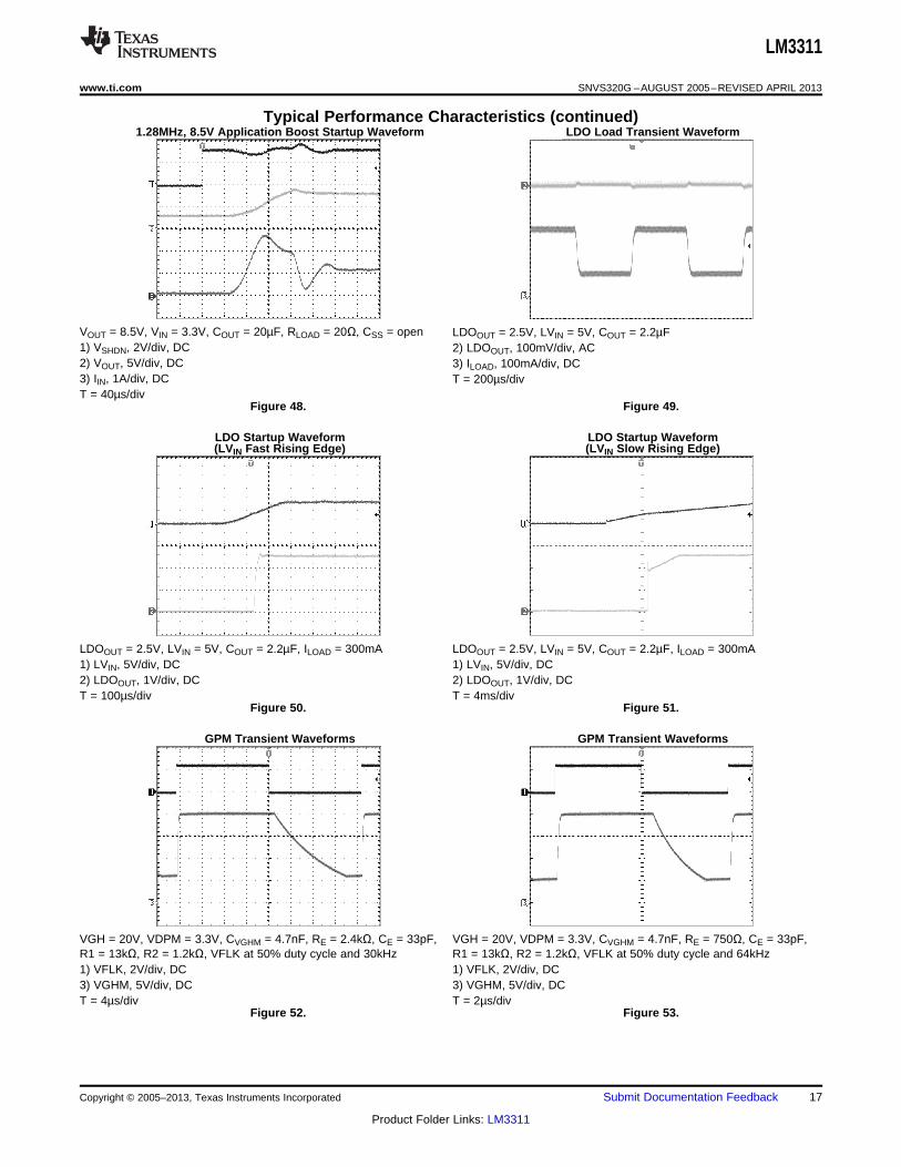
VOUT = 8.5V, VIN = 3.3V, COUT = 20µF, RLOAD = 20Ω, CSS = open LDOOUT = 2.5V, LVIN = 5V, COUT = 2.2µF1) VSHDN, 2V/div, DC 2) LDOOUT, 100mV/div, AC2) VOUT, 5V/div, DC 3) ILOAD, 100mA/div, DC3) IIN, 1A/div, DC T = 200µs/divT = 40µs/div
Figure 48. Figure 49.
LDO Startup Waveform LDO Startup Waveform(LVIN Fast Rising Edge) (LVIN Slow Rising Edge)
LDOOUT = 2.5V, LVIN = 5V, COUT = 2.2µF, ILOAD = 300mA LDOOUT = 2.5V, LVIN = 5V, COUT = 2.2µF, ILOAD = 300mA1) LVIN, 5V/div, DC 1) LVIN, 5V/div, DC2) LDOOUT, 1V/div, DC 2) LDOOUT, 1V/div, DCT = 100µs/div T = 4ms/div
Figure 50. Figure 51.
GPM Transient Waveforms GPM Transient Waveforms
VGH = 20V, VDPM = 3.3V, CVGHM = 4.7nF, RE = 2.4kΩ, CE = 33pF, VGH = 20V, VDPM = 3.3V, CVGHM = 4.7nF, RE = 750Ω, CE = 33pF,R1 = 13kΩ, R2 = 1.2kΩ, VFLK at 50% duty cycle and 30kHz R1 = 13kΩ, R2 = 1.2kΩ, VFLK at 50% duty cycle and 64kHz1) VFLK, 2V/div, DC 1) VFLK, 2V/div, DC3) VGHM, 5V/div, DC 3) VGHM, 5V/div, DCT = 4µs/div T = 2µs/div
Figure 52. Figure 53.
Copyright © 2005–2013, Texas Instruments Incorporated Submit Documentation Feedback 17
Product Folder Links: LM3311

LM3311
SNVS320G –AUGUST 2005–REVISED APRIL 2013 www.ti.com
Typical Performance Characteristics (continued)GPM Transient Waveforms GPM Transient Waveforms
VGH = 20V, VDPM = 3.3V, CVGHM = 4.7nF, RE = 2.4kΩ, CE = open, VGH = 20V, VDPM = 3.3V, CVGHM = 4.7nF, RE = 750Ω, CE = open,R1 = 13kΩ, R2 = 1.2kΩ, VFLK at 50% duty cycle and 30kHz R1 = 13kΩ, R2 = 1.2kΩ, VFLK at 50% duty cycle and 64kHz1) VFLK, 2V/div, DC 1) VFLK, 2V/div, DC3) VGHM, 5V/div, DC 3) VGHM, 5V/div, DCT = 4µs/div T = 2µs/div
Figure 54. Figure 55.
18 Submit Documentation Feedback Copyright © 2005–2013, Texas Instruments Incorporated
Product Folder Links: LM3311

:RADJ1 = RADJ2 xLDO out - 1.263
1.263(LDO)
:RFB1 = RFB2 xVOUT - 1.263
1.263(Boost)
VOUT =VIN
1-D, D' = (1-D) =
VIN
VOUT
VIN COUT
PWM
L
RLOAD
VIN
L
COUT RLOAD
X
V IN
L
COUT RLOAD
Cycle 1 Cycle 2(a) (b)
+
VOUT
-
+
VOUT
-
D
LM3311
www.ti.com SNVS320G –AUGUST 2005–REVISED APRIL 2013
OPERATION
(a) First Cycle of Operation(b) Second Cycle Of Operation
Figure 56. Simplified Boost Converter Diagram
CONTINUOUS CONDUCTION MODE
The LM3311 contains a current-mode, PWM boost regulator. A boost regulator steps the input voltage up to ahigher output voltage. In continuous conduction mode (when the inductor current never reaches zero at steadystate), the boost regulator operates in two cycles.
In the first cycle of operation, shown in Figure 56 (a), the transistor is closed and the diode is reverse biased.Energy is collected in the inductor and the load current is supplied by COUT.
The second cycle is shown in Figure 56 (b). During this cycle, the transistor is open and the diode is forwardbiased. The energy stored in the inductor is transferred to the load and output capacitor.
The ratio of these two cycles determines the output voltage. The output voltage is defined approximately as:
where• D is the duty cycle of the switch• D and D′ will be required for design calculations (1)
SETTING THE OUTPUT VOLTAGE (BOOST CONVERTER AND LDO)
The output voltage is set using the feedback pin and a resistor divider connected to the output as shown in theTypical Application Circuit. The feedback pin voltage is 1.263V for both the boost regulator and the LDO, so theratio of the feedback resistors sets the output voltage according to the following equations:
(2)
(3)
Copyright © 2005–2013, Texas Instruments Incorporated Submit Documentation Feedback 19
Product Folder Links: LM3311

LM3311
SNVS320G –AUGUST 2005–REVISED APRIL 2013 www.ti.com
SOFT-START CAPACITOR
The LM3311 has a soft-start pin that can be used to limit the inductor inrush current on start-up. The external SSpin is used to tailor the soft-start for a specific application (see the LINEAR REGULATOR (LDO) section for theminimum value of CSS). When used, a current source charges the external soft-start capacitor CSS until it reachesits typical clamp voltage, VSS. The soft-start time can be estimated as:
TSS = CSS*VSS/ISS (4)
THERMAL SHUTDOWN
The LM3311 includes thermal shutdown. If the die temperature reaches 145°C the device will shut down until itcools to a safe temperature at which point the device will resume operation. If the adverse condition that isheating the device is not removed (ambient temperature too high, short circuit conditions, etc...) the device willcontinue to cycle on and off to keep the die temperature below 145°C. The thermal shutdown has approximately20°C of hysteresis. When in thermal shutdown the boost regulator, LDO, Op-Amp, and GPM blocks will all bedisabled.
INPUT UNDER-VOLTAGE PROTECTION
The LM3311 includes input under-voltage protection (UVP). The purpose of the UVP is to protect the device bothduring start-up and during normal operation from trying to operate with insufficient input voltage. During start-upusing a ramping input voltage the UVP circuitry ensures that the device does not begin switching until the inputvoltage reaches the UVP On threshold. If the input voltage is present and the shutdown pin is pulled high theUVP circuitry will prevent the device from switching if the input voltage present is lower than the UVP Onthreshold. During normal operation the UVP circuitry will disable the device if the input voltage falls below theUVP Off threshold for any reason. In this case the device will not turn back on until the UVP On threshold voltageis exceeded.
LINEAR REGULATOR (LDO)
The LM3311 includes a Low Dropout Linear Regulator. The LDO is designed to operate with ceramic input andoutput capacitors with values as low as 2.2µF. The efficiency of the LDO is approximately the output voltagedivided by the input voltage. When using higher input voltages special care should be taken to not dissipate toomuch power and cause excessive heating of the die. The power dissipated in the LDO section is approximately:
PD(LDO) = (VIN - VOUT)*IOUT (5)
The LDO has an output undervoltage lockout feature. This feature is to ensure the LDO will shut itself down inthe event of an output overload or short condition. When the output is overloaded the output voltage will fallcausing the ADJ voltage to fall. When the ADJ voltage falls to VADJ(LOW) the LDO will shut off. In this event theSHDN pin or the input UVP must be cycled to turn the LDO back on.
The LDO output undervoltage lockout is controlled by the SS voltage. The LDO startup time must be less thanthe following:
TS = CSS*0.5V/ISS (6)
When SS is less than 0.5V the output undervoltage lockout is disabled and allows the LDO to start up. When SSis greater than 0.5V the undervoltage lockout is active. If the LDO feedback voltage is not greater than VADJ(LOW)when SS reaches 0.5V the LDO may enter an undervoltage lockout condition. In most cases CSS = 10nF orgreater is sufficient. If a supply other than that used to power VIN is used to power LVIN care must be taken toapply the input voltage to LVIN prior to applying voltage to VIN.
OPERATIONAL AMPLIFIER
Compensation:
The architecture used for the amplifier in the LM3311 requires external compensation on the output. Dependingon the equivalent resistive and capacitive distributed load of the TFT-LCD panel, external components at theamplifier outputs may or may not be necessary. If the capacitance presented by the load is equal to or greaterthan an equivalent distibutive load of 50Ω in series with 4.7nF no external components are needed as the TFT-LCD panel will act as compensation itself. Distributed resistive and capacitive loads enhance stability andincrease performance of the amplifiers. If the capacitance and resistance presented by the load is less than 50Ωin series with 4.7nF, external components will be required as the load itself will not ensure stability. No external
20 Submit Documentation Feedback Copyright © 2005–2013, Texas Instruments Incorporated
Product Folder Links: LM3311

LM3311
www.ti.com SNVS320G –AUGUST 2005–REVISED APRIL 2013
compensation in this case will lead to oscillation of the amplifier and an increase in power consumption. A goodchoice for compensation in this case is to add a 50Ω in series with a 4.7nF capacitor from the output of theamplifier to ground. This allows for driving zero to infinite capacitance loads with no oscillations, minimalovershoot, and a higher slew rate than using a single large capacitor. The high phase margin created by theexternal compensation will ensure stability and good performance for all conditions.
Layout and Filtering considerations:
When the power supply for the amplifier (AVIN) is connected to the output of the switching regulator, the outputripple of the regulator will produce ripple at the output of the amplifiers. This can be minimized by directlybypassing the AVIN pin to ground with a low ESR ceramic capacitor. For best noise reduction a resistor on theorder of 5Ω to 20Ω from the supply being used to the AVIN pin will create and RC filter and give you a cleanersupply to the amplifier. The bypass capacitor should be placed as close to the AVIN pin as possible andconnected directly to the AGND plane.
For best noise immunity all bias and feedback resistors should be in the low kΩ range due to the high inputimpedance of the amplifier. It is good practice to use a small capacitance at the high impedance input terminalsas well to reduce noise susceptibility. All resistors and capacitors should be placed as close to the input pins aspossible.
Special care should also be taken in routing of the PCB traces. All traces should be as short and direct aspossible. The output pin trace must never be routed near any trace going to the positive input. If this happenscross talk from the output trace to the positive input trace will cause the circuit to oscillate.
The op-amp is not a three terminal device it has 5 terminals: positive voltage power pin, AGND, positive input,negative input, and the output. The op-amp "routes" current from the power pin and AGND to the output pin. Soin effect an opamp has not two inputs but four, all of which must be kept noise free relative to the external circuitswhich are being driven by the op-amp. The current from the power pins goes through the output pin and into theload and feedback loop. The current exiting the load and feedback loops then must have a return path back tothe op-amp power supply pins. Ideally this return path must follow the same path as the output pin trace to theload. Any deviation that makes the loop area larger between the output current path and the return current pathadds to the probability of noise pick up.
GATE PULSE MODULATION
The Gate Pulse Modulation (GPM) block is designed to provide a modulated voltage to the gate driver circuitry ofa TFT LCD display. Operation is best understood by referring to the GPM block diagram in the Block Diagramssection, the drawing in Figure 57 and the transient waveforms in Figure 58 and Figure 59.
There are two control signals in the GPM block, VDPM and VFLK. VDPM is the enable pin for the GPM block. IfVDPM is high, the GPM block is active and will respond to the VFLK drive signal from the timing controller.However, if VDPM is low, the GPM block will be disabled and both PMOS switches P2 and P3 will be turned off.The VGHM node will be discharged through a 1kΩ resistor and the NMOS switch N2.
When VDPM is high, typical waveforms for the GPM block can be seen in Figure 57. The pin VGH is typicallydriven by a 2x or 3x charge pump. In most cases, the 2x or 3x charge pump is a discrete solution driven from theSW pin and the output of the boost switching regulator. When VFLK is high, the PMOS switch P2 is turned onand the PMOS switch P3 is turned off. With P2 on, the VGHM pin is pulled to the same voltage applied to theVGH pin. This provides a high gate drive voltage, VGHMMAX, and can source current to the gate drive circuitry.When VFLK is high, NMOS switch N3 is on which discharges the capacitor CE.
Copyright © 2005–2013, Texas Instruments Incorporated Submit Documentation Feedback 21
Product Folder Links: LM3311

VGHMMAX
VGHMMIN
MR
~1.94V
0
0
0
t
t
t
VGHM
VFLK
CE
~1.265V
tDELAY
LM3311
SNVS320G –AUGUST 2005–REVISED APRIL 2013 www.ti.com
Figure 57.
When VFLK is low, the NMOS switch N3 is turned off which allows current to charge the CE capacitor. Thiscreates a delay, tDELAY, given by the following equations:
tDELAY ≊ 1.265V(CE + 15pF)/ICE (7)
When the voltage on CE reaches about 1.265V and the VFLK signal is low, the PMOS switch P2 will turn off andthe PMOS switch P3 will turn on connecting resistor R3 to the VGHM pin through P3. This will discharge thevoltage at VGHM at some rate determined by R3 creating a slope, MR, as shown in Figure 57. The VGHM pin isno longer a current source, it is now sinking current from the gate drive circuitry.
As VGHM is discharged through R3, the comparator connected to the pin VDD monitors the VGHM voltage.PMOS switch P3 will turn off when the following is true:
VGHMMIN ≊ 10VXR2/(R1 + R2)
where• VX is some voltage connected to the resistor divider on pin VDD (8)
VX is typically connected to the output of the boost switching regulator. When PMOS switch P3 turns off, VGHMwill be high impedance until the VFLK pin is high again.
Figure 58 and Figure 59 give typical transient waveforms for the GPM block. Waveform (1) is the VGHM pin, (2)is the VFLK and (3) is the VDPM. The output of the boost switching regulator is operating at 8.5V and there is a3x discrete charge pump (~23.5V) supplying the VGH pin. In Figure 58 and Figure 59, the VGHM pin is driving apurely capacitive load, 4.7nF. The value of resistor R1 is 15kohm, R2 is 1.1kΩ and R3 is 750Ω. In both transientplots, there is no CE delay capacitor.
22 Submit Documentation Feedback Copyright © 2005–2013, Texas Instruments Incorporated
Product Folder Links: LM3311

LM3311
www.ti.com SNVS320G –AUGUST 2005–REVISED APRIL 2013
Figure 58. Waveform
Figure 59. Waveform
In the GPM block diagram, a signal called “Reset” is shown. This signal is generated from the VIN under-voltagelockout, thermal shutdown, or the SHDN pin. If the VIN supply voltage drops below 2.3V, typically, then the GPMblock will be disabled and the VGHM pin will discharge through NMOS switch N2 and the 1kΩ resistor. Thisapplies also if the junction temperature of the device exceeds 145°C or if the SHDN signal is low. As shown inthe Block Diagrams, both VDPM and VFLK have internal 350kΩ pull down resistors. This puts both VDPM andVFLK in normally “off” states. Typical VDPM and VFLK pin currents can be found in the Typical PerformanceCharacteristics section.
Copyright © 2005–2013, Texas Instruments Incorporated Submit Documentation Feedback 23
Product Folder Links: LM3311

t (s)
t (s)
Li'IL_AVG
ID_AVG
=IOUT_AVG
D*Ts Ts
D*Ts Ts
IL (A)
ID (A)
LVIN
LVV OUTIN
LVV OUTIN
(a)
(b)
LM3311
SNVS320G –AUGUST 2005–REVISED APRIL 2013 www.ti.com
INTRODUCTION TO COMPENSATION (BOOST CONVERTER)
(a) Inductor current(b) Diode current
Figure 60.
The LM3311 is a current mode PWM boost converter. The signal flow of this control scheme has two feedbackloops, one that senses switch current and one that senses output voltage.
To keep a current programmed control converter stable above duty cycles of 50%, the inductor must meetcertain criteria. The inductor, along with input and output voltage, will determine the slope of the current throughthe inductor (see Figure 60 (a)). If the slope of the inductor current is too great, the circuit will be unstable aboveduty cycles of 50%. A 10µH inductor is recommended for most 660 kHz applications, while a 4.7µH inductor maybe used for most 1.28 MHz applications. If the duty cycle is approaching the maximum of 85%, it may benecessary to increase the inductance by as much as 2X. See INDUCTOR AND DIODE SELECTION for moredetailed inductor sizing.
The LM3311 provides a compensation pin (VC) to customize the voltage loop feedback. It is recommended that aseries combination of RC and CC be used for the compensation network, as shown in the Typical ApplicationCircuit. For any given application, there exists a unique combination of RC and CC that will optimize theperformance of the LM3311 circuit in terms of its transient response. The series combination of RC and CCintroduces a pole-zero pair according to the following equations:
24 Submit Documentation Feedback Copyright © 2005–2013, Texas Instruments Incorporated
Product Folder Links: LM3311

iL(AVE) + 'iL iL(PEAK) |
IOUT
KD'iL(AVE) |
'iL = (in Amps)VIND
2Lfs
VINRDSON
0.144 fsL >
D
D'- 1 (in H)
Hz1
2S(RC + RO)CCfPC =
Hz1
fZC = 2SRCCC
LM3311
www.ti.com SNVS320G –AUGUST 2005–REVISED APRIL 2013
(9)
where• RO is the output impedance of the error amplifier, approximately 900kΩ (10)
For most applications, performance can be optimized by choosing values within the range 5kΩ ≤ RC ≤ 100kΩ (RCcan be higher values if CC2 is used, see HIGH OUTPUT CAPACITOR ESR COMPENSATION) and 68pF ≤ CC ≤4.7nF. Refer to the Application Information section for recommended values for specific circuits and conditions.Refer to the COMPENSATION section for other design requirement.
COMPENSATION
This section will present a general design procedure to help insure a stable and operational circuit. The designsin this datasheet are optimized for particular requirements. If different conversions are required, some of thecomponents may need to be changed to ensure stability. Below is a set of general guidelines in designing astable circuit for continuous conduction operation, in most all cases this will provide for stability duringdiscontinuous operation as well. The power components and their effects will be determined first, then thecompensation components will be chosen to produce stability.
INDUCTOR AND DIODE SELECTION
Although the inductor sizes mentioned earlier are fine for most applications, a more exact value can becalculated. To ensure stability at duty cycles above 50%, the inductor must have some minimum valuedetermined by the minimum input voltage and the maximum output voltage. This equation is:
where• fs is the switching frequency• D is the duty cycle• RDSON is the ON resistance of the internal power switch (11)
This equation is only good for duty cycles greater than 50% (D>0.5), for duty cycles less than 50% therecommended values may be used. The value given by this equation is the inductance necessary to supresssub-harmonic oscillations. In some cases the value given by this equation may be too small for a givenapplication. In this case the average inductor current and the inductor current ripple must be considered.
The corresponding inductor current ripple, average inductor current, and peak inductor current as shown inFigure 60 (a) is given by:
(12)
(13)
(14)
Continuous conduction mode occurs when ΔiL is less than the average inductor current and discontinuousconduction mode occurs when ΔiL is greater than the average inductor current. Care must be taken to make surethat the switch will not reach its current limit during normal operation. The inductor must also be sizedaccordingly. It should have a saturation current rating higher than the peak inductor current expected. The outputvoltage ripple is also affected by the total ripple current.
Copyright © 2005–2013, Texas Instruments Incorporated Submit Documentation Feedback 25
Product Folder Links: LM3311
m1 #VINRDSON
L(in V/s)
n = 1+2mc
m1(no unit)
Leff = L
(D')2
Zc (in rad/s)2fs
nD'#
ADC(DB) = 20log10 [(ZcLeff)// RL]//RL (in dB)RFB1 + RFB2
RFB2
( )gmROD'
RDSON
LM3311
SNVS320G –AUGUST 2005–REVISED APRIL 2013 www.ti.com
The output diode for a boost regulator must be chosen correctly depending on the output voltage and the outputcurrent. The typical current waveform for the diode in continuous conduction mode is shown in Figure 60 (b). Thediode must be rated for a reverse voltage equal to or greater than the output voltage used. The average currentrating must be greater than the maximum load current expected, and the peak current rating must be greaterthan the peak inductor current. During short circuit testing, or if short circuit conditions are possible in theapplication, the diode current rating must exceed the switch current limit. Using Schottky diodes with lowerforward voltage drop will decrease power dissipation and increase efficiency.
DC GAIN AND OPEN-LOOP GAIN
Since the control stage of the converter forms a complete feedback loop with the power components, it forms aclosed-loop system that must be stabilized to avoid positive feedback and instability. A value for open-loop DCgain will be required, from which you can calculate, or place, poles and zeros to determine the crossoverfrequency and the phase margin. A high phase margin (greater than 45°) is desired for the best stability andtransient response. For the purpose of stabilizing the LM3311, choosing a crossover point well below where theright half plane zero is located will ensure sufficient phase margin.
To ensure a bandwidth of ½ or less of the frequency of the RHP zero, calculate the open-loop DC gain, ADC.After this value is known, you can calculate the crossover visually by placing a −20dB/decade slope at each pole,and a +20dB/decade slope for each zero. The point at which the gain plot crosses unity gain, or 0dB, is thecrossover frequency. If the crossover frequency is less than ½ the RHP zero, the phase margin should be highenough for stability. The phase margin can also be improved by adding CC2 as discussed later in this section.The equation for ADC is given below with additional equations required for the calculation:
where• RL is the minimum load resistance• gm is the error amplifier transconductance found in the Electrical Characteristics table (15)
(16)
(17)
(18)mc ≊ 0.072fs (in V/s) (19)
• VIN is the minimum input voltage• RDSON is the value chosen from the graph "NMOS RDSON vs. Input Voltage" in the Typical Performance
Characteristics (20)
INPUT AND OUTPUT CAPACITOR SELECTION
The switching action of a boost regulator causes a triangular voltage waveform at the input. A capacitor isrequired to reduce the input ripple and noise for proper operation of the regulator. The size used is dependant onthe application and board layout. If the regulator will be loaded uniformly, with very little load changes, and atlower current outputs, the input capacitor size can often be reduced. The size can also be reduced if the input ofthe regulator is very close to the source output. The size will generally need to be larger for applications wherethe regulator is supplying nearly the maximum rated output or if large load steps are expected. A minimum valueof 10µF should be used for the less stressful condtions while a 22µF to 47µF capacitor may be required forhigher power and dynamic loads. Larger values and/or lower ESR may be needed if the application requires verylow ripple on the input source voltage.
26 Submit Documentation Feedback Copyright © 2005–2013, Texas Instruments Incorporated
Product Folder Links: LM3311

fZC =1
2SCCRC(in Hz)
fPC =1
2S(RC + RO)CC(in Hz)
(in Hz)RHPzero =VOUT(D')2
2S,LOADL
fZ1 =1
2SRESRCOUT(in Hz)
fP1 =1
2S(RESR + RL)COUT(in Hz)
LM3311
www.ti.com SNVS320G –AUGUST 2005–REVISED APRIL 2013
The choice of output capacitors is also somewhat arbitrary and depends on the design requirements for outputvoltage ripple. It is recommended that low ESR (Equivalent Series Resistance, denoted RESR) capacitors be usedsuch as ceramic, polymer electrolytic, or low ESR tantalum. Higher ESR capacitors may be used but will requiremore compensation which will be explained later on in the section. The ESR is also important because itdetermines the peak to peak output voltage ripple according to the approximate equation:
ΔVOUT ≊ 2ΔiLRESR (in Volts) (21)
A minimum value of 10µF is recommended and may be increased to a larger value. After choosing the outputcapacitor you can determine a pole-zero pair introduced into the control loop by the following equations:
where• RL is the minimum load resistance corresponding to the maximum load current (22)
(23)
The zero created by the ESR of the output capacitor is generally very high frequency if the ESR is small. If lowESR capacitors are used it can be neglected. If higher ESR capacitors are used see the HIGH OUTPUTCAPACITOR ESR COMPENSATION section. Some suitable capacitor vendors include Vishay, Taiyo-Yuden,and TDK.
RIGHT HALF PLANE ZERO
A current mode control boost regulator has an inherent right half plane zero (RHP zero). This zero has the effectof a zero in the gain plot, causing an imposed +20dB/decade on the rolloff, but has the effect of a pole in thephase, subtracting another 90° in the phase plot. This can cause undesirable effects if the control loop isinfluenced by this zero. To ensure the RHP zero does not cause instability issues, the control loop should bedesigned to have a bandwidth of less than ½ the frequency of the RHP zero. This zero occurs at a frequency of:
where• ILOAD is the maximum load current (24)
SELECTING THE COMPENSATION COMPONENTS
The first step in selecting the compensation components RC and CC is to set a dominant low frequency pole inthe control loop. Simply choose values for RC and CC within the ranges given in the Introduction toCompensation section to set this pole in the area of 10Hz to 500Hz. The frequency of the pole created isdetermined by the equation:
where• RO is the output impedance of the error amplifier, approximately 900kΩ (25)
Since RC is generally much less than RO, it does not have much effect on the above equation and can beneglected until a value is chosen to set the zero fZC. fZC is created to cancel out the pole created by the outputcapacitor, fP1. The output capacitor pole will shift with different load currents as shown by the equation, so settingthe zero is not exact. Determine the range of fP1 over the expected loads and then set the zero fZC to a pointapproximately in the middle. The frequency of this zero is determined by:
(26)
Now RC can be chosen with the selected value for CC. Check to make sure that the pole fPC is still in the 10Hz to500Hz range, change each value slightly if needed to ensure both component values are in the recommendedrange.
Copyright © 2005–2013, Texas Instruments Incorporated Submit Documentation Feedback 27
Product Folder Links: LM3311

fPC2 =1
2SCC2(RC //RO)(in Hz)
LM3311
SNVS320G –AUGUST 2005–REVISED APRIL 2013 www.ti.com
HIGH OUTPUT CAPACITOR ESR COMPENSATION
When using an output capacitor with a high ESR value, or just to improve the overall phase margin of the controlloop, another pole may be introduced to cancel the zero created by the ESR. This is accomplished by addinganother capacitor, CC2, directly from the compensation pin VC to ground, in parallel with the series combination ofRC and CC. The pole should be placed at the same frequency as fZ1, the ESR zero. The equation for this polefollows:
(27)
To ensure this equation is valid, and that CC2 can be used without negatively impacting the effects of RC and CC,fPC2 must be greater than 10fZC.
CHECKING THE DESIGN
With all the poles and zeros calculated the crossover frequency can be checked as described in the section DCGAIN AND OPEN-LOOP GAIN. The compensation values can be changed a little more to optimize performanceif desired. This is best done in the lab on a bench, checking the load step response with different values until theringing and overshoot on the output voltage at the edge of the load steps is minimal. This should produce astable, high performance circuit. For improved transient response, higher values of RC should be chosen. Thiswill improve the overall bandwidth which makes the regulator respond more quickly to transients. If more detail isrequired, or the most optimum performance is desired, refer to a more in depth discussion of compensatingcurrent mode DC/DC switching regulators.
POWER DISSIPATION
The output power of the LM3311 is limited by its maximum power dissipation. The maximum power dissipation isdetermined by the formula
PD = (Tjmax - TA)/θJA
where• Tjmax is the maximum specified junction temperature (125°C)• TA is the ambient temperature• θJA is the thermal resistance of the package (28)
LAYOUT CONSIDERATIONS
The input bypass capacitor CIN, as shown in the Typical Application Circuit, must be placed close to the IC. Thiswill reduce copper trace resistance which effects input voltage ripple of the IC. For additional input voltagefiltering, a 100nF bypass capacitor can be placed in parallel with CIN, close to the VIN pin, to shunt any highfrequency noise to ground. The output capacitor, COUT, should also be placed close to the IC. Any copper traceconnections for the COUT capacitor can increase the series resistance, which directly effects output voltage ripple.The feedback network, resistors RFB1 and RFB2, should be kept close to the FB pin, and away from the inductor,to minimize copper trace connections that can inject noise into the system. RE and CE should also be close to theRE and CE pins to minimize noise in the GPM circuitry. Trace connections made to the inductor and schottkydiode should be minimized to reduce power dissipation and increase overall efficiency. For more detail onswitching power supply layout considerations see Application Note AN-1149: Layout Guidelines for SwitchingPower Supplies (SNVA021).
The input capacitor, output capacitor, and feedback resistors for the LDO should be placed as close to the deviceas possible to minimize noise and increase stability. Keep the feedback traces short and connect RADJ2 directly toAGND close to the device.
For Op-Amp layout please refer to the OPERATIONAL AMPLIFIER section.
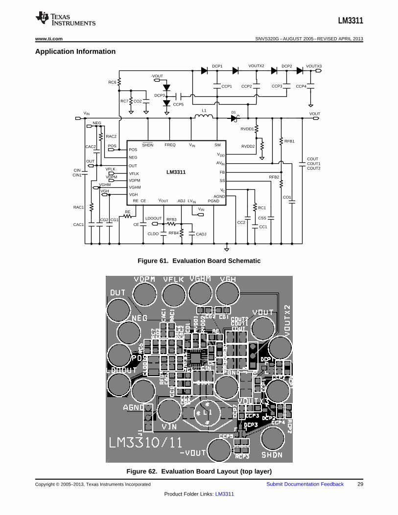
Figure 61, Figure 62, and Figure 63 in the Application Information section following show the schematic and anexample of a good layout as used in the LM3310/11 evaluation board.
28 Submit Documentation Feedback Copyright © 2005–2013, Texas Instruments Incorporated
Product Folder Links: LM3311
VDD
LVIN
CINCIN1
COUTCOUT1COUT2
VIN
FB
SW
ADJ
SS
AGNDVOUT
POS
NEG
SHDN FREQ
LM3311
VC
DCP1
CADJ
D1L1
RFB1
VIN
PGND
OUT
VDPM
VGHM
VFLK
CERE
VGH
RE
CE
LDOOUT
AVIN
CCP1
RVDD1
RVDD2
VOUTX2
RFB2
RFB3
RFB4CLDO
CSS
CC1
RC1VIN
CC2
VOUT
CCP2
DCP2
CCP3
VOUTX3
CCP4
CCP5
DCP3
-VOUT
CG1CG2
POS
RC6
RC7 CO2
NEG
RAC2
CAC2
CAC1
RAC1
OUT
VFLK
VDPM
VGHM
VGH
CO1
LM3311
www.ti.com SNVS320G –AUGUST 2005–REVISED APRIL 2013
Application Information
Figure 61. Evaluation Board Schematic
Figure 62. Evaluation Board Layout (top layer)
Copyright © 2005–2013, Texas Instruments Incorporated Submit Documentation Feedback 29
Product Folder Links: LM3311

VDD
LVIN
CSS
CIN
COUT
VIN
FB
SW
ADJ
SS
AGNDVOUT
POS
NEG
SHDN FREQ
LM3311
VC
D3D2
C2 C1
D1L
RFB1160k
VIN
CC
RC
PGND
OUT
VDPM
VGHM
VFLK
CERE
VGH
RE
CE
= 15V
LDO Output2.5V
AVIN
RADJ1
RADJ2
C3 C4
R1
R2
VOUT
VOH
22 PF
2 X 10 PFceramic
RFB230k
10 PH
2.4k
33 pF
12k
12k2.2 PF 2.2 PF
13k
1.2k
10 nF
1 nF
30k
1 PF 1 PF
= 8V = 2.9V - 4.2V
VIN
Connect to VGH
68 pFCC2
LM3311
SNVS320G –AUGUST 2005–REVISED APRIL 2013 www.ti.com
Figure 63. Evaluation Board Layout (bottom layer)
Figure 64. Li-Ion to 8V, 1.28MHz Application
30 Submit Documentation Feedback Copyright © 2005–2013, Texas Instruments Incorporated
Product Folder Links: LM3311
VDD
LVIN
CSS
CIN
COUT
VIN
FB
SW
ADJ
SS
AGNDVOUT
POS
NEG
SHDN FREQ
LM3311
VC
D3D2
C2 C1
D1L
RFB116k
VIN
CC
RC
PGND
OUT
VDPM
VGHM
VFLK
CERE
VGH
RE
CE
= 20V
LDO Output2.5V
AVIN
RADJ1
RADJ2
C3 C4
R1
R2
VOUT
VOH
22 PF
4 X 10 PFceramic
RFB22.2k
10 PH
2.4k
33 pF
12k
12k2.2 PF 2.2 PF
13k
1.2k
10 nF
100 pF
33k
CFF33 pF
1 PF 1 PF
= 10.5V = 5V
VIN
Connect to VGH
LM3311
www.ti.com SNVS320G –AUGUST 2005–REVISED APRIL 2013
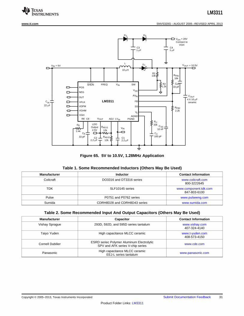
Figure 65. 5V to 10.5V, 1.28MHz Application
Table 1. Some Recommended Inductors (Others May Be Used)
Manufacturer Inductor Contact Information
Coilcraft DO3316 and DT3316 series www.coilcraft.com800-3222645
TDK SLF10145 series www.component.tdk.com847-803-6100
Pulse P0751 and P0762 series www.pulseeng.com
Sumida CDRH8D28 and CDRH8D43 series www.sumida.com
Table 2. Some Recommended Input And Output Capacitors (Others May Be Used)
Manufacturer Capacitor Contact Information
Vishay Sprague 293D, 592D, and 595D series tantalum www.vishay.com407-324-4140
Taiyo Yuden High capacitance MLCC ceramic www.t-yuden.com408-573-4150
ESRD seriec Polymer Aluminum ElectrolyticCornell Dubilier www.cde.comSPV and AFK series V-chip series
High capacitance MLCC ceramicPanasonic www.panasonic.comEEJ-L series tantalum
Copyright © 2005–2013, Texas Instruments Incorporated Submit Documentation Feedback 31
Product Folder Links: LM3311

LM3311
SNVS320G –AUGUST 2005–REVISED APRIL 2013 www.ti.com
REVISION HISTORY
Changes from Revision F (April 2013) to Revision G Page
• Changed layout of National Data Sheet to TI format .......................................................................................................... 31
32 Submit Documentation Feedback Copyright © 2005–2013, Texas Instruments Incorporated
Product Folder Links: LM3311

PACKAGE OPTION ADDENDUM
www.ti.com 23-Sep-2013
Addendum-Page 1
PACKAGING INFORMATION
Orderable Device Status(1)
Package Type PackageDrawing
Pins PackageQty
Eco Plan(2)
Lead/Ball Finish MSL Peak Temp(3)
Op Temp (°C) Device Marking(4/5)
Samples
LM3311SQ-HIOP ACTIVE WQFN RTW 24 TBD Call TI Call TI L3311HP
LM3311SQ-HIOP/NOPB ACTIVE WQFN RTW 24 1000 Green (RoHS& no Sb/Br)
CU SN Level-1-260C-UNLIM L3311HP
LM3311SQX ACTIVE WQFN RTW 24 TBD Call TI Call TI -40 to 125 L3311SQ
LM3311SQX-HIOP ACTIVE WQFN RTW 24 TBD Call TI Call TI -40 to 125 L3311HP
LM3311SQX-HIOP/NOPB ACTIVE WQFN RTW 24 4500 Green (RoHS& no Sb/Br)
CU SN Level-1-260C-UNLIM -40 to 125 L3311HP
LM3311SQX/NOPB ACTIVE WQFN RTW 24 4500 Green (RoHS& no Sb/Br)
CU SN Level-1-260C-UNLIM -40 to 125 L3311SQ
(1) The marketing status values are defined as follows:ACTIVE: Product device recommended for new designs.LIFEBUY: TI has announced that the device will be discontinued, and a lifetime-buy period is in effect.NRND: Not recommended for new designs. Device is in production to support existing customers, but TI does not recommend using this part in a new design.PREVIEW: Device has been announced but is not in production. Samples may or may not be available.OBSOLETE: TI has discontinued the production of the device.
(2) Eco Plan - The planned eco-friendly classification: Pb-Free (RoHS), Pb-Free (RoHS Exempt), or Green (RoHS & no Sb/Br) - please check http://www.ti.com/productcontent for the latest availabilityinformation and additional product content details.TBD: The Pb-Free/Green conversion plan has not been defined.Pb-Free (RoHS): TI's terms "Lead-Free" or "Pb-Free" mean semiconductor products that are compatible with the current RoHS requirements for all 6 substances, including the requirement thatlead not exceed 0.1% by weight in homogeneous materials. Where designed to be soldered at high temperatures, TI Pb-Free products are suitable for use in specified lead-free processes.Pb-Free (RoHS Exempt): This component has a RoHS exemption for either 1) lead-based flip-chip solder bumps used between the die and package, or 2) lead-based die adhesive used betweenthe die and leadframe. The component is otherwise considered Pb-Free (RoHS compatible) as defined above.Green (RoHS & no Sb/Br): TI defines "Green" to mean Pb-Free (RoHS compatible), and free of Bromine (Br) and Antimony (Sb) based flame retardants (Br or Sb do not exceed 0.1% by weightin homogeneous material)
(3) MSL, Peak Temp. -- The Moisture Sensitivity Level rating according to the JEDEC industry standard classifications, and peak solder temperature.
(4) There may be additional marking, which relates to the logo, the lot trace code information, or the environmental category on the device.
(5) Multiple Device Markings will be inside parentheses. Only one Device Marking contained in parentheses and separated by a "~" will appear on a device. If a line is indented then it is a continuationof the previous line and the two combined represent the entire Device Marking for that device.

PACKAGE OPTION ADDENDUM
www.ti.com 23-Sep-2013
Addendum-Page 2
Important Information and Disclaimer:The information provided on this page represents TI's knowledge and belief as of the date that it is provided. TI bases its knowledge and belief on informationprovided by third parties, and makes no representation or warranty as to the accuracy of such information. Efforts are underway to better integrate information from third parties. TI has taken andcontinues to take reasonable steps to provide representative and accurate information but may not have conducted destructive testing or chemical analysis on incoming materials and chemicals.TI and TI suppliers consider certain information to be proprietary, and thus CAS numbers and other limited information may not be available for release.
In no event shall TI's liability arising out of such information exceed the total purchase price of the TI part(s) at issue in this document sold by TI to Customer on an annual basis.

TAPE AND REEL INFORMATION
*All dimensions are nominal
Device PackageType
PackageDrawing
Pins SPQ ReelDiameter
(mm)
ReelWidth
W1 (mm)
A0(mm)
B0(mm)
K0(mm)
P1(mm)
W(mm)
Pin1Quadrant
LM3311SQ-HIOP/NOPB WQFN RTW 24 1000 178.0 12.4 4.3 4.3 1.3 8.0 12.0 Q1
LM3311SQX-HIOP/NOPB WQFN RTW 24 4500 330.0 12.4 4.3 4.3 1.3 8.0 12.0 Q1
LM3311SQX/NOPB WQFN RTW 24 4500 330.0 12.4 4.3 4.3 1.3 8.0 12.0 Q1
PACKAGE MATERIALS INFORMATION
www.ti.com 23-Sep-2013
Pack Materials-Page 1

*All dimensions are nominal
Device Package Type Package Drawing Pins SPQ Length (mm) Width (mm) Height (mm)
LM3311SQ-HIOP/NOPB WQFN RTW 24 1000 203.0 190.0 41.0
LM3311SQX-HIOP/NOPB WQFN RTW 24 4500 367.0 367.0 35.0
LM3311SQX/NOPB WQFN RTW 24 4500 367.0 367.0 35.0
PACKAGE MATERIALS INFORMATION
www.ti.com 23-Sep-2013
Pack Materials-Page 2

MECHANICAL DATA
RTW0024A
www.ti.com
SQA24A (Rev B)

IMPORTANT NOTICE
Texas Instruments Incorporated and its subsidiaries (TI) reserve the right to make corrections, enhancements, improvements and otherchanges to its semiconductor products and services per JESD46, latest issue, and to discontinue any product or service per JESD48, latestissue. Buyers should obtain the latest relevant information before placing orders and should verify that such information is current andcomplete. All semiconductor products (also referred to herein as “components”) are sold subject to TI’s terms and conditions of salesupplied at the time of order acknowledgment.
TI warrants performance of its components to the specifications applicable at the time of sale, in accordance with the warranty in TI’s termsand conditions of sale of semiconductor products. Testing and other quality control techniques are used to the extent TI deems necessaryto support this warranty. Except where mandated by applicable law, testing of all parameters of each component is not necessarilyperformed.
TI assumes no liability for applications assistance or the design of Buyers’ products. Buyers are responsible for their products andapplications using TI components. To minimize the risks associated with Buyers’ products and applications, Buyers should provideadequate design and operating safeguards.
TI does not warrant or represent that any license, either express or implied, is granted under any patent right, copyright, mask work right, orother intellectual property right relating to any combination, machine, or process in which TI components or services are used. Informationpublished by TI regarding third-party products or services does not constitute a license to use such products or services or a warranty orendorsement thereof. Use of such information may require a license from a third party under the patents or other intellectual property of thethird party, or a license from TI under the patents or other intellectual property of TI.
Reproduction of significant portions of TI information in TI data books or data sheets is permissible only if reproduction is without alterationand is accompanied by all associated warranties, conditions, limitations, and notices. TI is not responsible or liable for such altereddocumentation. Information of third parties may be subject to additional restrictions.
Resale of TI components or services with statements different from or beyond the parameters stated by TI for that component or servicevoids all express and any implied warranties for the associated TI component or service and is an unfair and deceptive business practice.TI is not responsible or liable for any such statements.
Buyer acknowledges and agrees that it is solely responsible for compliance with all legal, regulatory and safety-related requirementsconcerning its products, and any use of TI components in its applications, notwithstanding any applications-related information or supportthat may be provided by TI. Buyer represents and agrees that it has all the necessary expertise to create and implement safeguards whichanticipate dangerous consequences of failures, monitor failures and their consequences, lessen the likelihood of failures that might causeharm and take appropriate remedial actions. Buyer will fully indemnify TI and its representatives against any damages arising out of the useof any TI components in safety-critical applications.
In some cases, TI components may be promoted specifically to facilitate safety-related applications. With such components, TI’s goal is tohelp enable customers to design and create their own end-product solutions that meet applicable functional safety standards andrequirements. Nonetheless, such components are subject to these terms.
No TI components are authorized for use in FDA Class III (or similar life-critical medical equipment) unless authorized officers of the partieshave executed a special agreement specifically governing such use.
Only those TI components which TI has specifically designated as military grade or “enhanced plastic” are designed and intended for use inmilitary/aerospace applications or environments. Buyer acknowledges and agrees that any military or aerospace use of TI componentswhich have not been so designated is solely at the Buyer's risk, and that Buyer is solely responsible for compliance with all legal andregulatory requirements in connection with such use.
TI has specifically designated certain components as meeting ISO/TS16949 requirements, mainly for automotive use. In any case of use ofnon-designated products, TI will not be responsible for any failure to meet ISO/TS16949.
Products Applications
Audio www.ti.com/audio Automotive and Transportation www.ti.com/automotive
Amplifiers amplifier.ti.com Communications and Telecom www.ti.com/communications
Data Converters dataconverter.ti.com Computers and Peripherals www.ti.com/computers
DLP® Products www.dlp.com Consumer Electronics www.ti.com/consumer-apps
DSP dsp.ti.com Energy and Lighting www.ti.com/energy
Clocks and Timers www.ti.com/clocks Industrial www.ti.com/industrial
Interface interface.ti.com Medical www.ti.com/medical
Logic logic.ti.com Security www.ti.com/security
Power Mgmt power.ti.com Space, Avionics and Defense www.ti.com/space-avionics-defense
Microcontrollers microcontroller.ti.com Video and Imaging www.ti.com/video
RFID www.ti-rfid.com
OMAP Applications Processors www.ti.com/omap TI E2E Community e2e.ti.com
Wireless Connectivity www.ti.com/wirelessconnectivity
Mailing Address: Texas Instruments, Post Office Box 655303, Dallas, Texas 75265Copyright © 2013, Texas Instruments Incorporated