Embed Size (px)
Citation preview
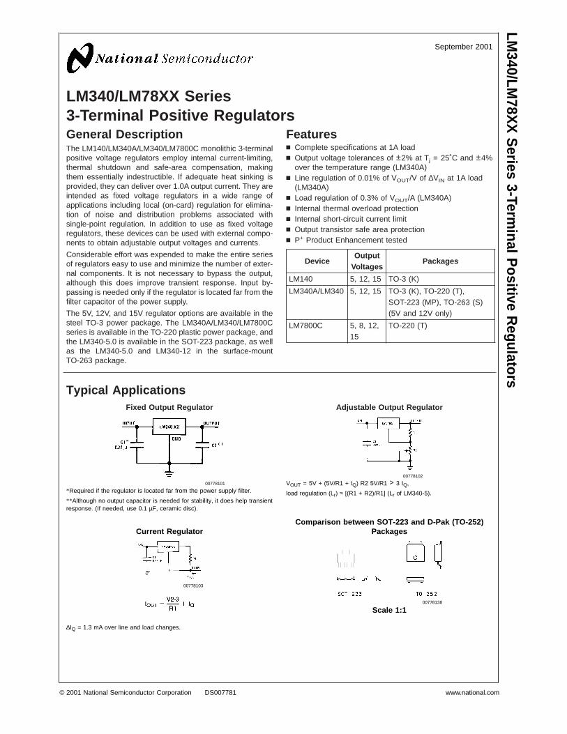
LM340/LM78XX Series3-Terminal Positive RegulatorsGeneral DescriptionThe LM140/LM340A/LM340/LM7800C monolithic 3-terminalpositive voltage regulators employ internal current-limiting,thermal shutdown and safe-area compensation, makingthem essentially indestructible. If adequate heat sinking isprovided, they can deliver over 1.0A output current. They areintended as fixed voltage regulators in a wide range ofapplications including local (on-card) regulation for elimina-tion of noise and distribution problems associated withsingle-point regulation. In addition to use as fixed voltageregulators, these devices can be used with external compo-nents to obtain adjustable output voltages and currents.
Considerable effort was expended to make the entire seriesof regulators easy to use and minimize the number of exter-nal components. It is not necessary to bypass the output,although this does improve transient response. Input by-passing is needed only if the regulator is located far from thefilter capacitor of the power supply.
The 5V, 12V, and 15V regulator options are available in thesteel TO-3 power package. The LM340A/LM340/LM7800Cseries is available in the TO-220 plastic power package, andthe LM340-5.0 is available in the SOT-223 package, as wellas the LM340-5.0 and LM340-12 in the surface-mountTO-263 package.
Featuresn Complete specifications at 1A loadn Output voltage tolerances of ±2% at Tj = 25˚C and ±4%
over the temperature range (LM340A)n Line regulation of 0.01% of VOUT/V of ∆VIN at 1A load
(LM340A)n Load regulation of 0.3% of VOUT/A (LM340A)n Internal thermal overload protectionn Internal short-circuit current limitn Output transistor safe area protectionn P+ Product Enhancement tested
DeviceOutput
VoltagesPackages
LM140 5, 12, 15 TO-3 (K)
LM340A/LM340 5, 12, 15 TO-3 (K), TO-220 (T),SOT-223 (MP), TO-263 (S)(5V and 12V only)
LM7800C 5, 8, 12,15
TO-220 (T)
Typical ApplicationsFixed Output Regulator Adjustable Output Regulator
00778101
*Required if the regulator is located far from the power supply filter.
**Although no output capacitor is needed for stability, it does help transientresponse. (If needed, use 0.1 µF, ceramic disc).
00778102
VOUT = 5V + (5V/R1 + IQ) R2 5V/R1 > 3 IQ,
load regulation (Lr) ≈ [(R1 + R2)/R1] (Lr of LM340-5).
Current RegulatorComparison between SOT-223 and D-Pak (TO-252)
Packages
00778103
∆IQ = 1.3 mA over line and load changes.
00778138
Scale 1:1
September 2001LM
340/LM78X
XS
eries3-Term
inalPositive
Regulators
© 2001 National Semiconductor Corporation DS007781 www.national.com
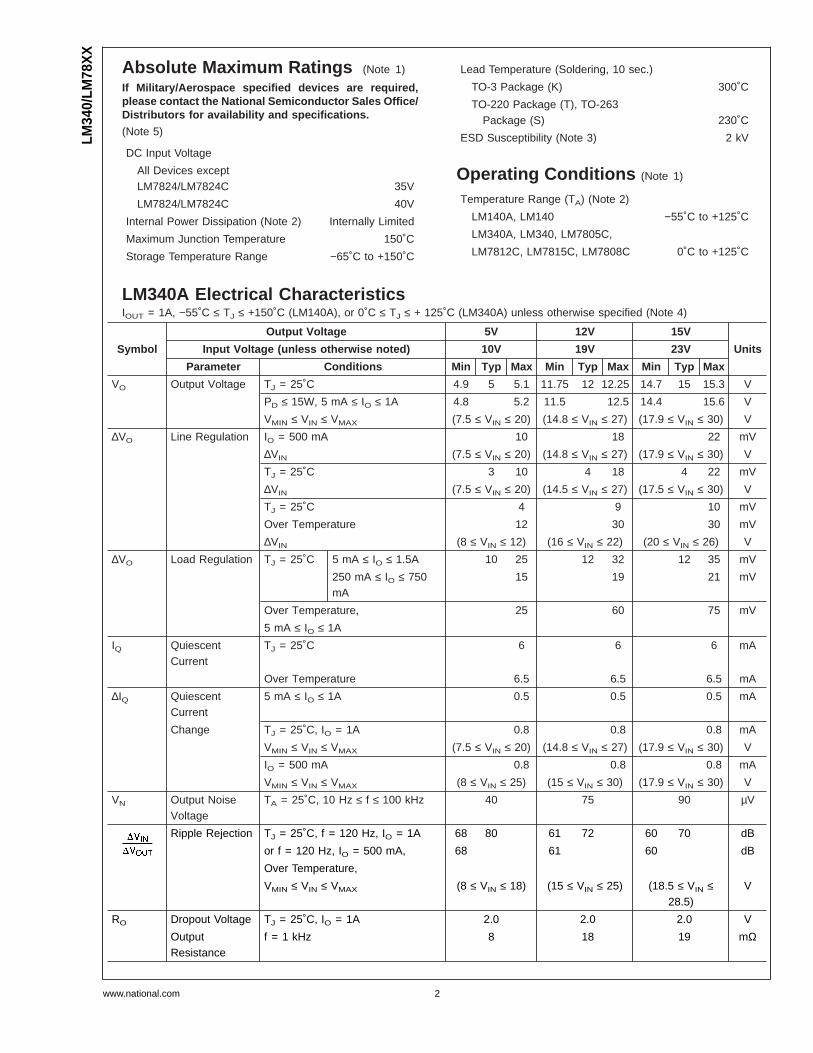
Absolute Maximum Ratings (Note 1)
If Military/Aerospace specified devices are required,please contact the National Semiconductor Sales Office/Distributors for availability and specifications.
(Note 5)
DC Input Voltage
All Devices exceptLM7824/LM7824C 35V
LM7824/LM7824C 40V
Internal Power Dissipation (Note 2) Internally Limited
Maximum Junction Temperature 150˚C
Storage Temperature Range −65˚C to +150˚C
Lead Temperature (Soldering, 10 sec.)
TO-3 Package (K) 300˚C
TO-220 Package (T), TO-263Package (S) 230˚C
ESD Susceptibility (Note 3) 2 kV
Operating Conditions (Note 1)
Temperature Range (TA) (Note 2)
LM140A, LM140 −55˚C to +125˚C
LM340A, LM340, LM7805C,
LM7812C, LM7815C, LM7808C 0˚C to +125˚C
LM340A Electrical CharacteristicsIOUT = 1A, −55˚C ≤ TJ ≤ +150˚C (LM140A), or 0˚C ≤ TJ ≤ + 125˚C (LM340A) unless otherwise specified (Note 4)
Output Voltage 5V 12V 15V
Symbol Input Voltage (unless otherwise noted) 10V 19V 23V Units
Parameter Conditions Min Typ Max Min Typ Max Min Typ Max
VO Output Voltage TJ = 25˚C 4.9 5 5.1 11.75 12 12.25 14.7 15 15.3 V
PD ≤ 15W, 5 mA ≤ IO ≤ 1A 4.8 5.2 11.5 12.5 14.4 15.6 V
VMIN ≤ VIN ≤ VMAX (7.5 ≤ VIN ≤ 20) (14.8 ≤ VIN ≤ 27) (17.9 ≤ VIN ≤ 30) V
∆VO Line Regulation IO = 500 mA 10 18 22 mV
∆VIN (7.5 ≤ VIN ≤ 20) (14.8 ≤ VIN ≤ 27) (17.9 ≤ VIN ≤ 30) V
TJ = 25˚C 3 10 4 18 4 22 mV
∆VIN (7.5 ≤ VIN ≤ 20) (14.5 ≤ VIN ≤ 27) (17.5 ≤ VIN ≤ 30) V
TJ = 25˚C 4 9 10 mV
Over Temperature 12 30 30 mV
∆VIN (8 ≤ VIN ≤ 12) (16 ≤ VIN ≤ 22) (20 ≤ VIN ≤ 26) V
∆VO Load Regulation TJ = 25˚C 5 mA ≤ IO ≤ 1.5A 10 25 12 32 12 35 mV
250 mA ≤ IO ≤ 750mA
15 19 21 mV
Over Temperature, 25 60 75 mV
5 mA ≤ IO ≤ 1A
IQ QuiescentCurrent
TJ = 25˚C 6 6 6 mA
Over Temperature 6.5 6.5 6.5 mA
∆IQ QuiescentCurrent
5 mA ≤ IO ≤ 1A 0.5 0.5 0.5 mA
Change TJ = 25˚C, IO = 1A 0.8 0.8 0.8 mA
VMIN ≤ VIN ≤ VMAX (7.5 ≤ VIN ≤ 20) (14.8 ≤ VIN ≤ 27) (17.9 ≤ VIN ≤ 30) V
IO = 500 mA 0.8 0.8 0.8 mA
VMIN ≤ VIN ≤ VMAX (8 ≤ VIN ≤ 25) (15 ≤ VIN ≤ 30) (17.9 ≤ VIN ≤ 30) V
VN Output NoiseVoltage
TA = 25˚C, 10 Hz ≤ f ≤ 100 kHz 40 75 90 µV
Ripple Rejection TJ = 25˚C, f = 120 Hz, IO = 1A 68 80 61 72 60 70 dB
or f = 120 Hz, IO = 500 mA, 68 61 60 dB
Over Temperature,
VMIN ≤ VIN ≤ VMAX (8 ≤ VIN ≤ 18) (15 ≤ VIN ≤ 25) (18.5 ≤ VIN ≤28.5)
V
RO Dropout Voltage TJ = 25˚C, IO = 1A 2.0 2.0 2.0 V
OutputResistance
f = 1 kHz 8 18 19 mΩ
LM34
0/LM
78X
X
www.national.com 2
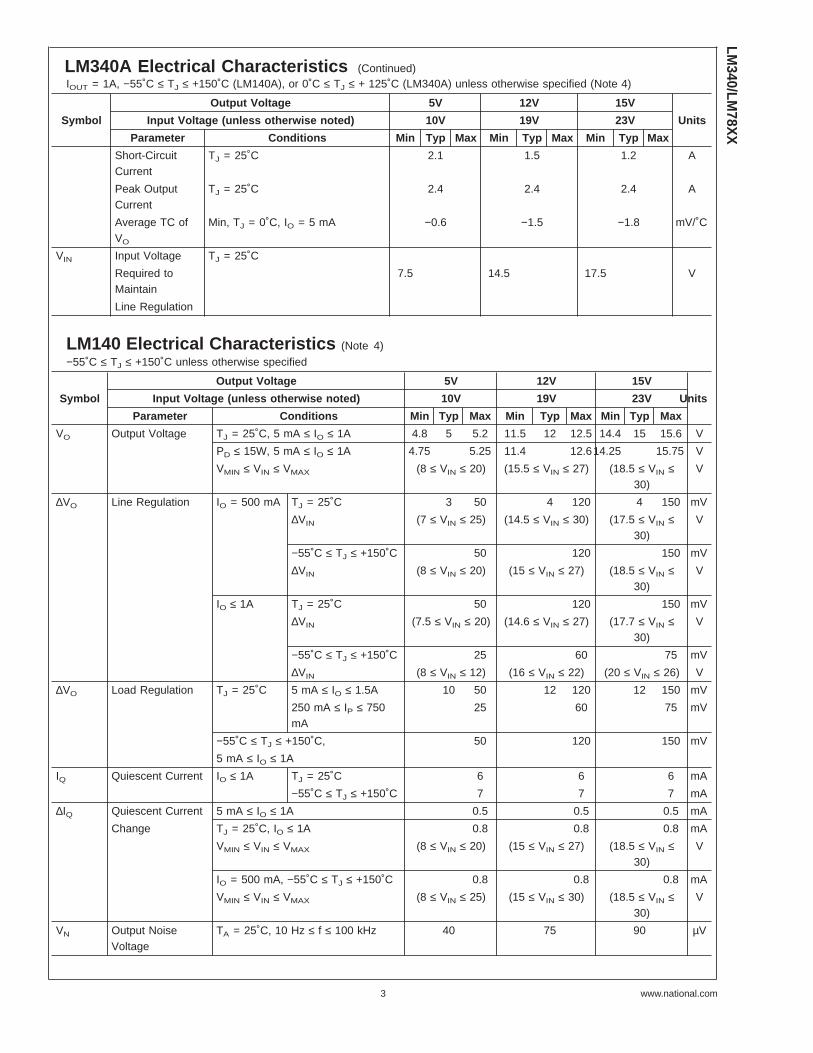
LM340A Electrical Characteristics (Continued)IOUT = 1A, −55˚C ≤ TJ ≤ +150˚C (LM140A), or 0˚C ≤ TJ ≤ + 125˚C (LM340A) unless otherwise specified (Note 4)
Output Voltage 5V 12V 15V
Symbol Input Voltage (unless otherwise noted) 10V 19V 23V Units
Parameter Conditions Min Typ Max Min Typ Max Min Typ Max
Short-CircuitCurrent
TJ = 25˚C 2.1 1.5 1.2 A
Peak OutputCurrent
TJ = 25˚C 2.4 2.4 2.4 A
Average TC ofVO
Min, TJ = 0˚C, IO = 5 mA −0.6 −1.5 −1.8 mV/˚C
VIN Input Voltage TJ = 25˚C
Required toMaintain
7.5 14.5 17.5 V
Line Regulation
LM140 Electrical Characteristics (Note 4)
−55˚C ≤ TJ ≤ +150˚C unless otherwise specified
Output Voltage 5V 12V 15V
Symbol Input Voltage (unless otherwise noted) 10V 19V 23V Units
Parameter Conditions Min Typ Max Min Typ Max Min Typ Max
VO Output Voltage TJ = 25˚C, 5 mA ≤ IO ≤ 1A 4.8 5 5.2 11.5 12 12.5 14.4 15 15.6 V
PD ≤ 15W, 5 mA ≤ IO ≤ 1A 4.75 5.25 11.4 12.614.25 15.75 V
VMIN ≤ VIN ≤ VMAX (8 ≤ VIN ≤ 20) (15.5 ≤ VIN ≤ 27) (18.5 ≤ VIN ≤30)
V
∆VO Line Regulation IO = 500 mA TJ = 25˚C 3 50 4 120 4 150 mV
∆VIN (7 ≤ VIN ≤ 25) (14.5 ≤ VIN ≤ 30) (17.5 ≤ VIN ≤30)
V
−55˚C ≤ TJ ≤ +150˚C 50 120 150 mV
∆VIN (8 ≤ VIN ≤ 20) (15 ≤ VIN ≤ 27) (18.5 ≤ VIN ≤30)
V
IO ≤ 1A TJ = 25˚C 50 120 150 mV
∆VIN (7.5 ≤ VIN ≤ 20) (14.6 ≤ VIN ≤ 27) (17.7 ≤ VIN ≤30)
V
−55˚C ≤ TJ ≤ +150˚C 25 60 75 mV
∆VIN (8 ≤ VIN ≤ 12) (16 ≤ VIN ≤ 22) (20 ≤ VIN ≤ 26) V
∆VO Load Regulation TJ = 25˚C 5 mA ≤ IO ≤ 1.5A 10 50 12 120 12 150 mV
250 mA ≤ IP ≤ 750mA
25 60 75 mV
−55˚C ≤ TJ ≤ +150˚C, 50 120 150 mV
5 mA ≤ IO ≤ 1A
IQ Quiescent Current IO ≤ 1A TJ = 25˚C 6 6 6 mA
−55˚C ≤ TJ ≤ +150˚C 7 7 7 mA
∆IQ Quiescent Current 5 mA ≤ IO ≤ 1A 0.5 0.5 0.5 mA
Change TJ = 25˚C, IO ≤ 1A 0.8 0.8 0.8 mA
VMIN ≤ VIN ≤ VMAX (8 ≤ VIN ≤ 20) (15 ≤ VIN ≤ 27) (18.5 ≤ VIN ≤30)
V
IO = 500 mA, −55˚C ≤ TJ ≤ +150˚C 0.8 0.8 0.8 mA
VMIN ≤ VIN ≤ VMAX (8 ≤ VIN ≤ 25) (15 ≤ VIN ≤ 30) (18.5 ≤ VIN ≤30)
V
VN Output NoiseVoltage
TA = 25˚C, 10 Hz ≤ f ≤ 100 kHz 40 75 90 µV
LM340/LM
78XX
www.national.com3
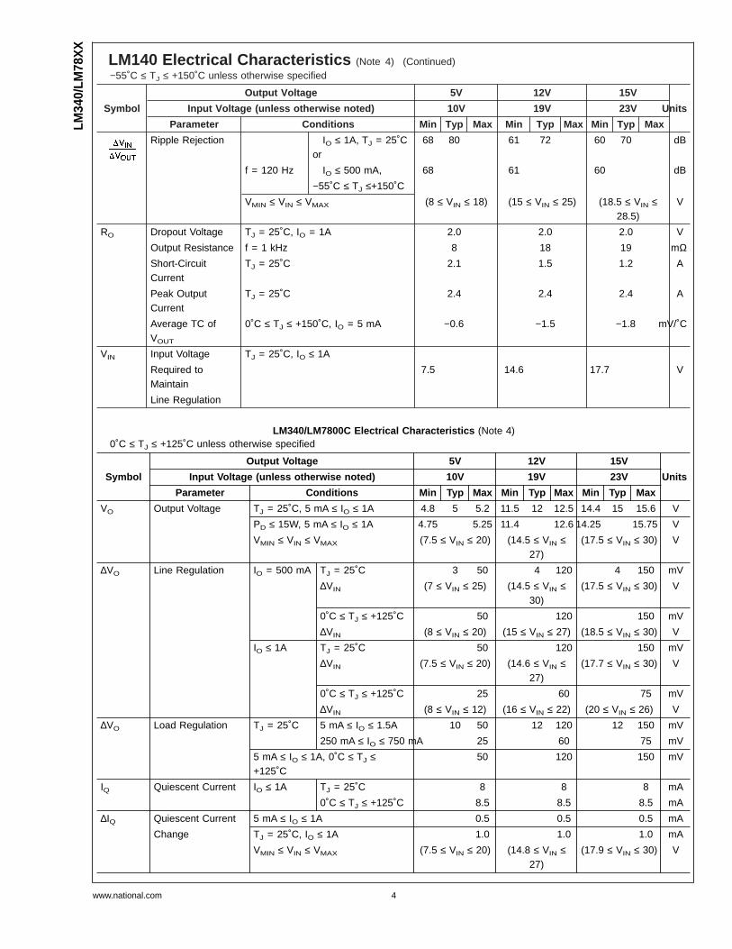
LM140 Electrical Characteristics (Note 4) (Continued)−55˚C ≤ TJ ≤ +150˚C unless otherwise specified
Output Voltage 5V 12V 15V
Symbol Input Voltage (unless otherwise noted) 10V 19V 23V Units
Parameter Conditions Min Typ Max Min Typ Max Min Typ Max
Ripple Rejection IO ≤ 1A, TJ = 25˚Cor
68 80 61 72 60 70 dB
f = 120 Hz IO ≤ 500 mA, 68 61 60 dB
−55˚C ≤ TJ ≤+150˚C
VMIN ≤ VIN ≤ VMAX (8 ≤ VIN ≤ 18) (15 ≤ VIN ≤ 25) (18.5 ≤ VIN ≤28.5)
V
RO Dropout Voltage TJ = 25˚C, IO = 1A 2.0 2.0 2.0 V
Output Resistance f = 1 kHz 8 18 19 mΩShort-CircuitCurrent
TJ = 25˚C 2.1 1.5 1.2 A
Peak OutputCurrent
TJ = 25˚C 2.4 2.4 2.4 A
Average TC ofVOUT
0˚C ≤ TJ ≤ +150˚C, IO = 5 mA −0.6 −1.5 −1.8 mV/˚C
VIN Input Voltage TJ = 25˚C, IO ≤ 1A
Required toMaintain
7.5 14.6 17.7 V
Line Regulation
LM340/LM7800C Electrical Characteristics (Note 4)0˚C ≤ TJ ≤ +125˚C unless otherwise specified
Output Voltage 5V 12V 15V
Symbol Input Voltage (unless otherwise noted) 10V 19V 23V Units
Parameter Conditions Min Typ Max Min Typ Max Min Typ Max
VO Output Voltage TJ = 25˚C, 5 mA ≤ IO ≤ 1A 4.8 5 5.2 11.5 12 12.5 14.4 15 15.6 V
PD ≤ 15W, 5 mA ≤ IO ≤ 1A 4.75 5.25 11.4 12.6 14.25 15.75 V
VMIN ≤ VIN ≤ VMAX (7.5 ≤ VIN ≤ 20) (14.5 ≤ VIN ≤27)
(17.5 ≤ VIN ≤ 30) V
∆VO Line Regulation IO = 500 mA TJ = 25˚C 3 50 4 120 4 150 mV
∆VIN (7 ≤ VIN ≤ 25) (14.5 ≤ VIN ≤30)
(17.5 ≤ VIN ≤ 30) V
0˚C ≤ TJ ≤ +125˚C 50 120 150 mV
∆VIN (8 ≤ VIN ≤ 20) (15 ≤ VIN ≤ 27) (18.5 ≤ VIN ≤ 30) V
IO ≤ 1A TJ = 25˚C 50 120 150 mV
∆VIN (7.5 ≤ VIN ≤ 20) (14.6 ≤ VIN ≤27)
(17.7 ≤ VIN ≤ 30) V
0˚C ≤ TJ ≤ +125˚C 25 60 75 mV
∆VIN (8 ≤ VIN ≤ 12) (16 ≤ VIN ≤ 22) (20 ≤ VIN ≤ 26) V
∆VO Load Regulation TJ = 25˚C 5 mA ≤ IO ≤ 1.5A 10 50 12 120 12 150 mV
250 mA ≤ IO ≤ 750 mA 25 60 75 mV
5 mA ≤ IO ≤ 1A, 0˚C ≤ TJ ≤+125˚C
50 120 150 mV
IQ Quiescent Current IO ≤ 1A TJ = 25˚C 8 8 8 mA
0˚C ≤ TJ ≤ +125˚C 8.5 8.5 8.5 mA
∆IQ Quiescent Current 5 mA ≤ IO ≤ 1A 0.5 0.5 0.5 mA
Change TJ = 25˚C, IO ≤ 1A 1.0 1.0 1.0 mA
VMIN ≤ VIN ≤ VMAX (7.5 ≤ VIN ≤ 20) (14.8 ≤ VIN ≤27)
(17.9 ≤ VIN ≤ 30) V
LM34
0/LM
78X
X
www.national.com 4
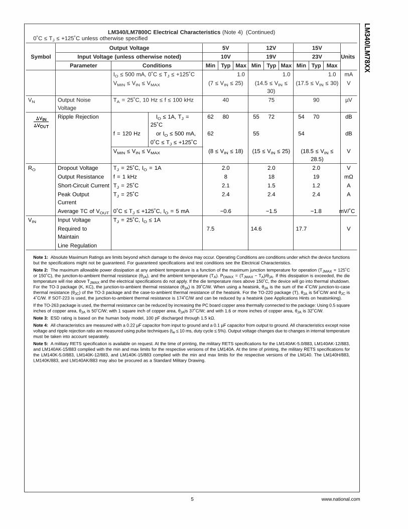
LM340/LM7800C Electrical Characteristics (Note 4) (Continued)0˚C ≤ TJ ≤ +125˚C unless otherwise specified
Output Voltage 5V 12V 15V
Symbol Input Voltage (unless otherwise noted) 10V 19V 23V Units
Parameter Conditions Min Typ Max Min Typ Max Min Typ Max
IO ≤ 500 mA, 0˚C ≤ TJ ≤ +125˚C 1.0 1.0 1.0 mA
VMIN ≤ VIN ≤ VMAX (7 ≤ VIN ≤ 25) (14.5 ≤ VIN ≤30)
(17.5 ≤ VIN ≤ 30) V
VN Output NoiseVoltage
TA = 25˚C, 10 Hz ≤ f ≤ 100 kHz 40 75 90 µV
Ripple Rejection IO ≤ 1A, TJ =25˚C
62 80 55 72 54 70 dB
f = 120 Hz or IO ≤ 500 mA, 62 55 54 dB
0˚C ≤ TJ ≤ +125˚C
VMIN ≤ VIN ≤ VMAX (8 ≤ VIN ≤ 18) (15 ≤ VIN ≤ 25) (18.5 ≤ VIN ≤28.5)
V
RO Dropout Voltage TJ = 25˚C, IO = 1A 2.0 2.0 2.0 V
Output Resistance f = 1 kHz 8 18 19 mΩShort-Circuit Current TJ = 25˚C 2.1 1.5 1.2 A
Peak OutputCurrent
TJ = 25˚C 2.4 2.4 2.4 A
Average TC of VOUT 0˚C ≤ TJ ≤ +125˚C, IO = 5 mA −0.6 −1.5 −1.8 mV/˚C
VIN Input Voltage TJ = 25˚C, IO ≤ 1A
Required toMaintain
7.5 14.6 17.7 V
Line Regulation
Note 1: Absolute Maximum Ratings are limits beyond which damage to the device may occur. Operating Conditions are conditions under which the device functionsbut the specifications might not be guaranteed. For guaranteed specifications and test conditions see the Electrical Characteristics.
Note 2: The maximum allowable power dissipation at any ambient temperature is a function of the maximum junction temperature for operation (TJMAX = 125˚Cor 150˚C), the junction-to-ambient thermal resistance (θJA), and the ambient temperature (TA). PDMAX = (TJMAX − TA)/θJA. If this dissipation is exceeded, the dietemperature will rise above TJMAX and the electrical specifications do not apply. If the die temperature rises above 150˚C, the device will go into thermal shutdown.For the TO-3 package (K, KC), the junction-to-ambient thermal resistance (θJA) is 39˚C/W. When using a heatsink, θJA is the sum of the 4˚C/W junction-to-casethermal resistance (θJC) of the TO-3 package and the case-to-ambient thermal resistance of the heatsink. For the TO-220 package (T), θJA is 54˚C/W and θJC is4˚C/W. If SOT-223 is used, the junction-to-ambient thermal resistance is 174˚C/W and can be reduced by a heatsink (see Applications Hints on heatsinking).
If the TO-263 package is used, the thermal resistance can be reduced by increasing the PC board copper area thermally connected to the package: Using 0.5 squareinches of copper area, θJA is 50˚C/W; with 1 square inch of copper area, θJAis 37˚C/W; and with 1.6 or more inches of copper area, θJA is 32˚C/W.
Note 3: ESD rating is based on the human body model, 100 pF discharged through 1.5 kΩ.
Note 4: All characteristics are measured with a 0.22 µF capacitor from input to ground and a 0.1 µF capacitor from output to ground. All characteristics except noisevoltage and ripple rejection ratio are measured using pulse techniques (tw ≤ 10 ms, duty cycle ≤ 5%). Output voltage changes due to changes in internal temperaturemust be taken into account separately.
Note 5: A military RETS specification is available on request. At the time of printing, the military RETS specifications for the LM140AK-5.0/883, LM140AK-12/883,and LM140AK-15/883 complied with the min and max limits for the respective versions of the LM140A. At the time of printing, the military RETS specifications forthe LM140K-5.0/883, LM140K-12/883, and LM140K-15/883 complied with the min and max limits for the respective versions of the LM140. The LM140H/883,LM140K/883, and LM140AK/883 may also be procured as a Standard Military Drawing.
LM340/LM
78XX
www.national.com5
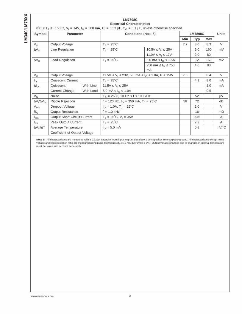
LM7808CElectrical Characteristics
0˚C ≤ TJ ≤ +150˚C, VI = 14V, IO = 500 mA, CI = 0.33 µF, CO = 0.1 µF, unless otherwise specified
Symbol Parameter Conditions (Note 6) LM7808C Units
Min Typ Max
VO Output Voltage TJ = 25˚C 7.7 8.0 8.3 V
∆VO Line Regulation TJ = 25˚C 10.5V ≤ VI ≤ 25V 6.0 160 mV
11.0V ≤ VI ≤ 17V 2.0 80
∆VO Load Regulation TJ = 25˚C 5.0 mA ≤ IO ≤ 1.5A 12 160 mV
250 mA ≤ IO ≤ 750mA
4.0 80
VO Output Voltage 11.5V ≤ VI ≤ 23V, 5.0 mA ≤ IO ≤ 1.0A, P ≤ 15W 7.6 8.4 V
IQ Quiescent Current TJ = 25˚C 4.3 8.0 mA
∆IQ Quiescent With Line 11.5V ≤ VI ≤ 25V 1.0 mA
Current Change With Load 5.0 mA ≤ IO ≤ 1.0A 0.5
VN Noise TA = 25˚C, 10 Hz ≤ f ≤ 100 kHz 52 µV
∆VI/∆VO Ripple Rejection f = 120 Hz, IO = 350 mA, TJ = 25˚C 56 72 dB
VDO Dropout Voltage IO = 1.0A, TJ = 25˚C 2.0 V
RO Output Resistance f = 1.0 kHz 16 mΩIOS Output Short Circuit Current TJ = 25˚C, VI = 35V 0.45 A
IPK Peak Output Current TJ = 25˚C 2.2 A
∆VO/∆T Average Temperature IO = 5.0 mA 0.8 mV/˚C
Coefficient of Output Voltage
Note 6: All characteristics are measured with a 0.22 µF capacitor from input to ground and a 0.1 µF capacitor from output to ground. All characteristics except noisevoltage and ripple rejection ratio are measured using pulse techniques (tw ≤ 10 ms, duty cycle ≤ 5%). Output voltage changes due to changes in internal temperaturemust be taken into account separately.
LM34
0/LM
78X
X
www.national.com 6
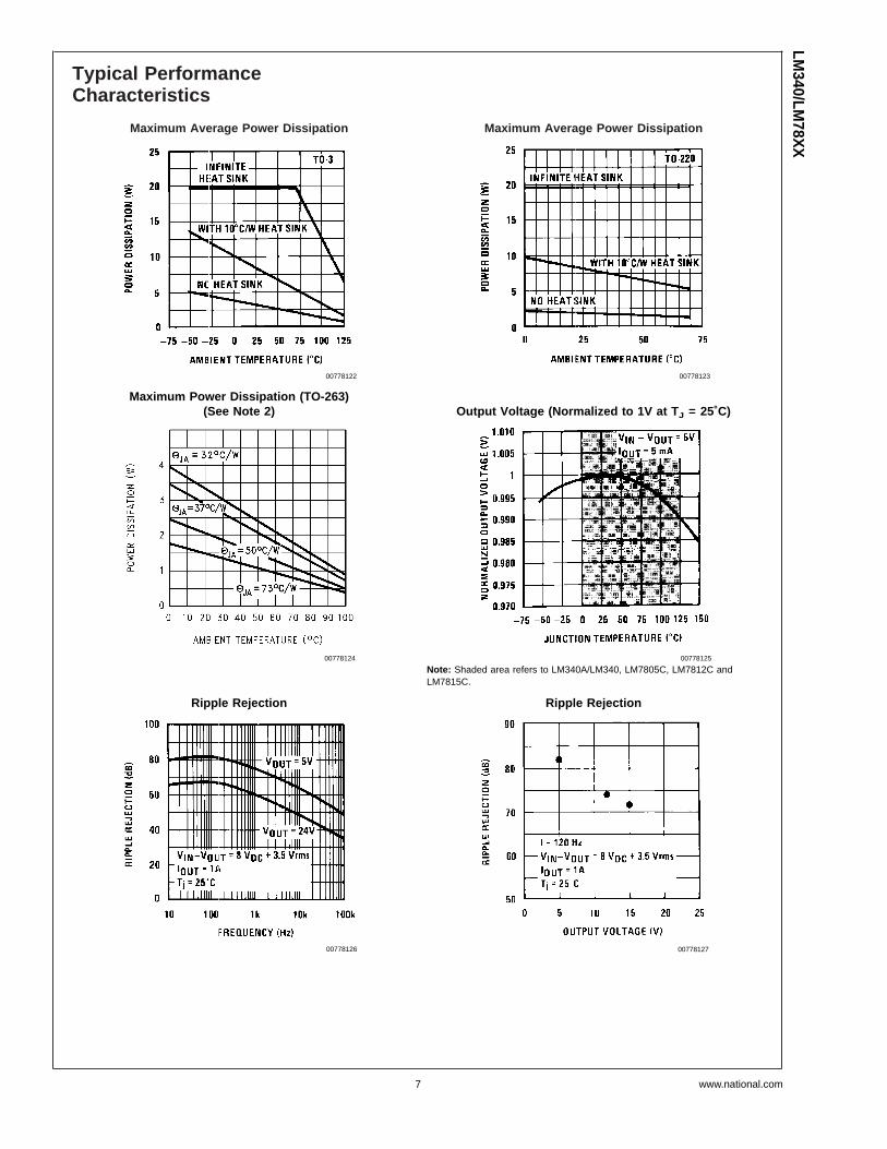
Typical PerformanceCharacteristics
Maximum Average Power Dissipation Maximum Average Power Dissipation
00778122 00778123
Maximum Power Dissipation (TO-263)(See Note 2) Output Voltage (Normalized to 1V at T J = 25˚C)
00778124 00778125
Note: Shaded area refers to LM340A/LM340, LM7805C, LM7812C andLM7815C.
Ripple Rejection Ripple Rejection
00778126 00778127
LM340/LM
78XX
www.national.com7
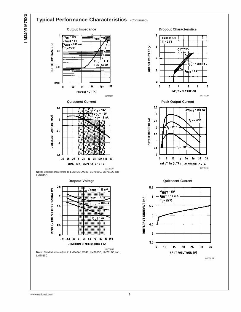
Typical Performance Characteristics (Continued)
Output Impedance Dropout Characteristics
00778128 00778129
Quiescent Current Peak Output Current
00778130
Note: Shaded area refers to LM340A/LM340, LM7805C, LM7812C andLM7815C.
00778131
Dropout Voltage Quiescent Current
00778132
Note: Shaded area refers to LM340A/LM340, LM7805C, LM7812C andLM7815C.
00778133
LM34
0/LM
78X
X
www.national.com 8
Line Regulation140AK-5.0, IOUT = 1A, TA = 25˚C
Line Regulation140AK-5.0, VIN = 10V, TA = 25˚C
00778105 00778106
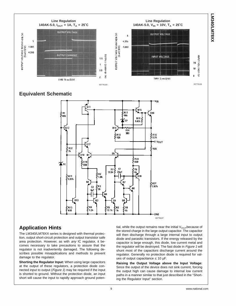
Equivalent Schematic
00778107
Application HintsThe LM340/LM78XX series is designed with thermal protec-tion, output short-circuit protection and output transistor safearea protection. However, as with any IC regulator, it be-comes necessary to take precautions to assure that theregulator is not inadvertently damaged. The following de-scribes possible misapplications and methods to preventdamage to the regulator.
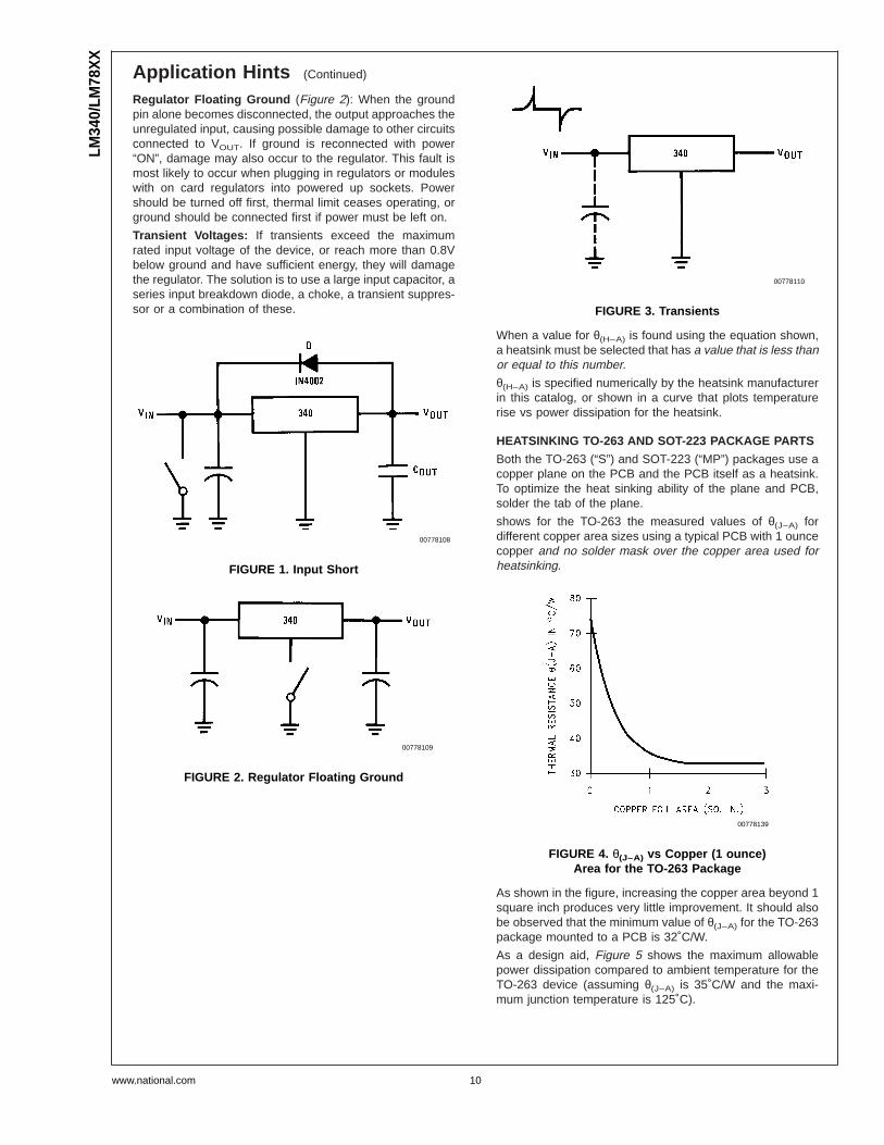
Shorting the Regulator Input: When using large capacitorsat the output of these regulators, a protection diode con-nected input to output (Figure 1) may be required if the inputis shorted to ground. Without the protection diode, an inputshort will cause the input to rapidly approach ground poten-
tial, while the output remains near the initial VOUTbecause ofthe stored charge in the large output capacitor. The capacitorwill then discharge through a large internal input to outputdiode and parasitic transistors. If the energy released by thecapacitor is large enough, this diode, low current metal andthe regulator will be destroyed. The fast diode in Figure 1 willshunt most of the capacitors discharge current around theregulator. Generally no protection diode is required for val-ues of output capacitance ≤ 10 µF.
Raising the Output Voltage above the Input Voltage:Since the output of the device does not sink current, forcingthe output high can cause damage to internal low currentpaths in a manner similar to that just described in the “Short-ing the Regulator Input” section.
LM340/LM
78XX
www.national.com9
Application Hints (Continued)
Regulator Floating Ground (Figure 2): When the groundpin alone becomes disconnected, the output approaches theunregulated input, causing possible damage to other circuitsconnected to VOUT. If ground is reconnected with power“ON”, damage may also occur to the regulator. This fault ismost likely to occur when plugging in regulators or moduleswith on card regulators into powered up sockets. Powershould be turned off first, thermal limit ceases operating, orground should be connected first if power must be left on.
Transient Voltages: If transients exceed the maximumrated input voltage of the device, or reach more than 0.8Vbelow ground and have sufficient energy, they will damagethe regulator. The solution is to use a large input capacitor, aseries input breakdown diode, a choke, a transient suppres-sor or a combination of these.
When a value for θ(H–A) is found using the equation shown,a heatsink must be selected that has a value that is less thanor equal to this number.
θ(H–A) is specified numerically by the heatsink manufacturerin this catalog, or shown in a curve that plots temperaturerise vs power dissipation for the heatsink.
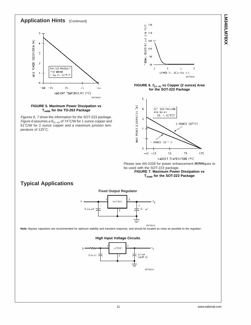
HEATSINKING TO-263 AND SOT-223 PACKAGE PARTS
Both the TO-263 (“S”) and SOT-223 (“MP”) packages use acopper plane on the PCB and the PCB itself as a heatsink.To optimize the heat sinking ability of the plane and PCB,solder the tab of the plane.
shows for the TO-263 the measured values of θ(J–A) fordifferent copper area sizes using a typical PCB with 1 ouncecopper and no solder mask over the copper area used forheatsinking.
As shown in the figure, increasing the copper area beyond 1square inch produces very little improvement. It should alsobe observed that the minimum value of θ(J–A) for the TO-263package mounted to a PCB is 32˚C/W.
As a design aid, Figure 5 shows the maximum allowablepower dissipation compared to ambient temperature for theTO-263 device (assuming θ(J–A) is 35˚C/W and the maxi-mum junction temperature is 125˚C).
00778108
FIGURE 1. Input Short
00778109
FIGURE 2. Regulator Floating Ground
00778110
FIGURE 3. Transients
00778139
FIGURE 4. θ(J–A) vs Copper (1 ounce)Area for the TO-263 Package
LM34
0/LM
78X
X
www.national.com 10
Application Hints (Continued)
Figures 6, 7 show the information for the SOT-223 package.Figure 6 assumes a θ(J–A) of 74˚C/W for 1 ounce copper and51˚C/W for 2 ounce copper and a maximum junction tem-perature of 125˚C.
Please see AN-1028 for power enhancement techniques tobe used with the SOT-223 package.
Typical ApplicationsFixed Output Regulator
00778113
Note: Bypass capacitors are recommended for optimum stability and transient response, and should be located as close as possible to the regulator.
High Input Voltage Circuits
00778114
00778140
FIGURE 5. Maximum Power Dissipation vsTAMB for the TO-263 Package
00778141
FIGURE 6. θ(J–A) vs Copper (2 ounce) Areafor the SOT-223 Package
00778142
FIGURE 7. Maximum Power Dissipation vsTAMB for the SOT-223 Package
LM340/LM
78XX
www.national.com11
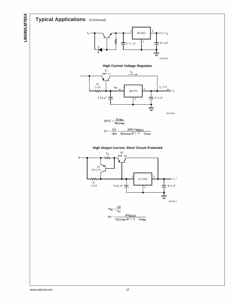
Typical Applications (Continued)
00778115
High Current Voltage Regulator
00778116
High Output Current, Short Circuit Protected
00778117
LM34
0/LM
78X
X
www.national.com 12
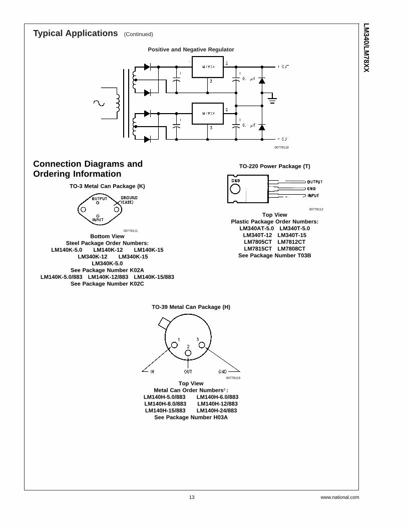
Typical Applications (Continued)
Positive and Negative Regulator
00778118
Connection Diagrams andOrdering Information
TO-3 Metal Can Package (K)
00778111
Bottom ViewSteel Package Order Numbers:
LM140K-5.0 LM140K-12 LM140K-15LM340K-12 LM340K-15
LM340K-5.0See Package Number K02A
LM140K-5.0/883 LM140K-12/883 LM140K-15/883See Package Number K02C
TO-220 Power Package (T)
00778112
Top ViewPlastic Package Order Numbers:
LM340AT-5.0 LM340T-5.0LM340T-12 LM340T-15LM7805CT LM7812CTLM7815CT LM7808CT
See Package Number T03B
TO-39 Metal Can Package (H)
00778119
Top ViewMetal Can Order Numbers †:
LM140H-5.0/883 LM140H-6.0/883LM140H-8.0/883 LM140H-12/883LM140H-15/883 LM140H-24/883
See Package Number H03A
LM340/LM
78XX
www.national.com13
Connection Diagrams andOrdering Information (Continued)
TO-263 Surface-Mount Package (S)
00778120
Top View
00778121
Side ViewSurface-Mount Package Order Numbers:
LM340S-5.0 LM340S-12See Package Number TS3B
3-Lead SOT-223(Front View)
Order Number LM340MP-5.0Package Marked NO0A
See Package Number MA04A
00778143
†The specifications for the LM140H/883 devices are not contained in this datasheet. If specifications for these devicesare required, contact the National Semiconductor Sales Office/Distributors.
LM34
0/LM
78X
X
www.national.com 14
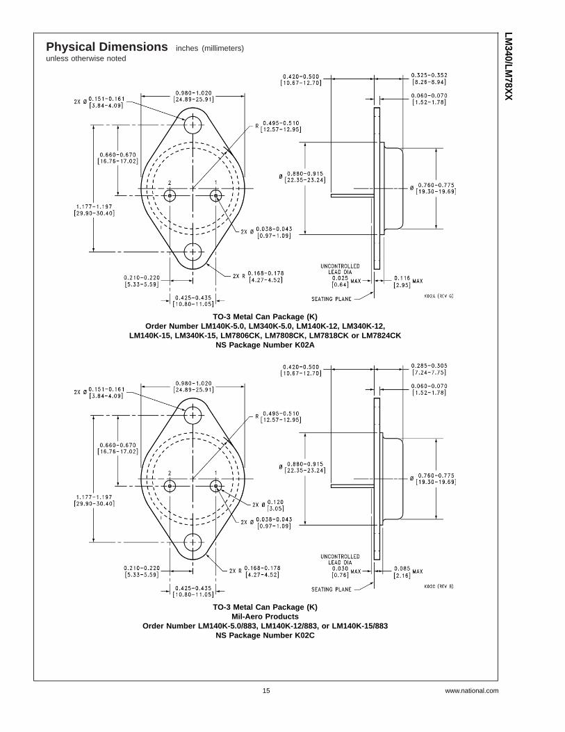
Physical Dimensions inches (millimeters)unless otherwise noted
TO-3 Metal Can Package (K)Order Number LM140K-5.0, LM340K-5.0, LM140K-12, LM340K-12,
LM140K-15, LM340K-15, LM7806CK, LM7808CK, LM7818CK or LM7824CKNS Package Number K02A
TO-3 Metal Can Package (K)Mil-Aero Products
Order Number LM140K-5.0/883, LM140K-12/883, or LM140K-15/883NS Package Number K02C
LM340/LM
78XX
www.national.com15
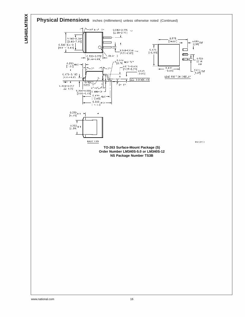
Physical Dimensions inches (millimeters) unless otherwise noted (Continued)
TO-263 Surface-Mount Package (S)Order Number LM340S-5.0 or LM340S-12
NS Package Number TS3B
LM34
0/LM
78X
X
www.national.com 16
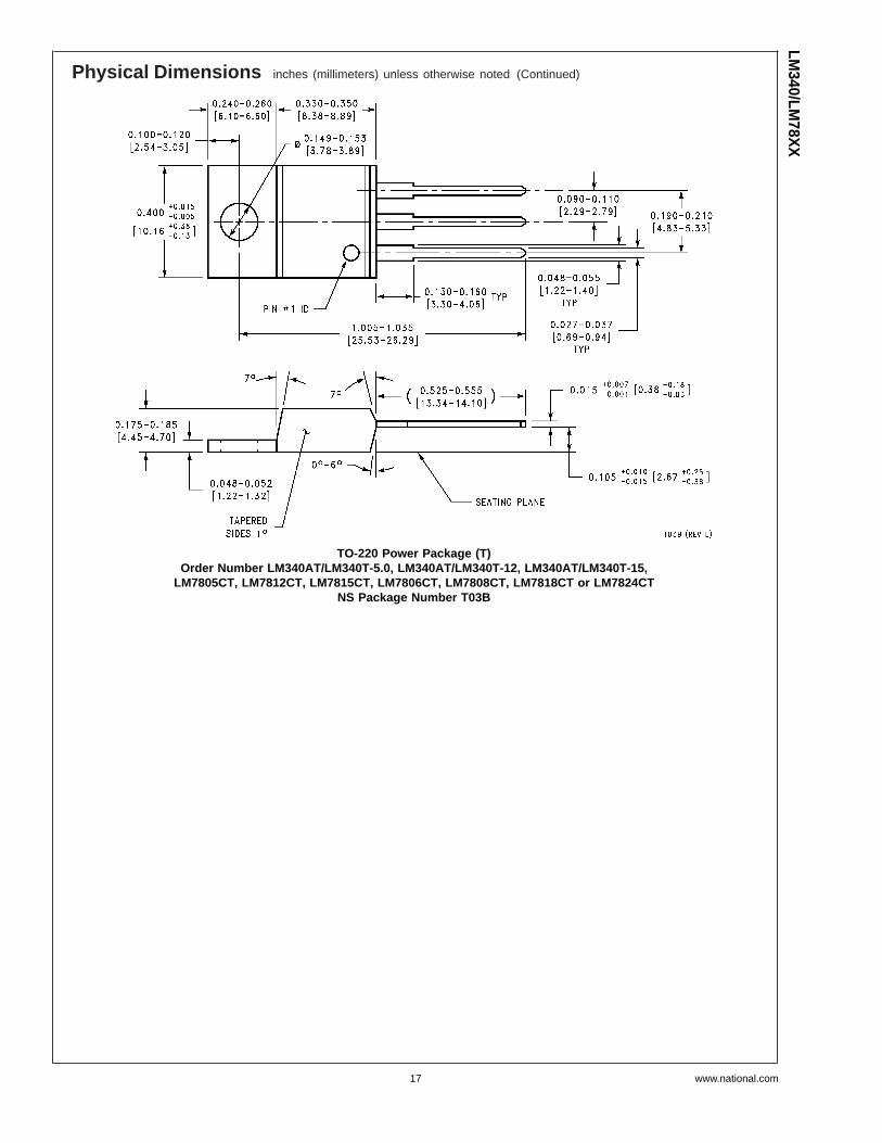
Physical Dimensions inches (millimeters) unless otherwise noted (Continued)
TO-220 Power Package (T)Order Number LM340AT/LM340T-5.0, LM340AT/LM340T-12, LM340AT/LM340T-15,
LM7805CT, LM7812CT, LM7815CT, LM7806CT, LM7808CT, LM7818CT or LM7824CTNS Package Number T03B
LM340/LM
78XX
www.national.com17
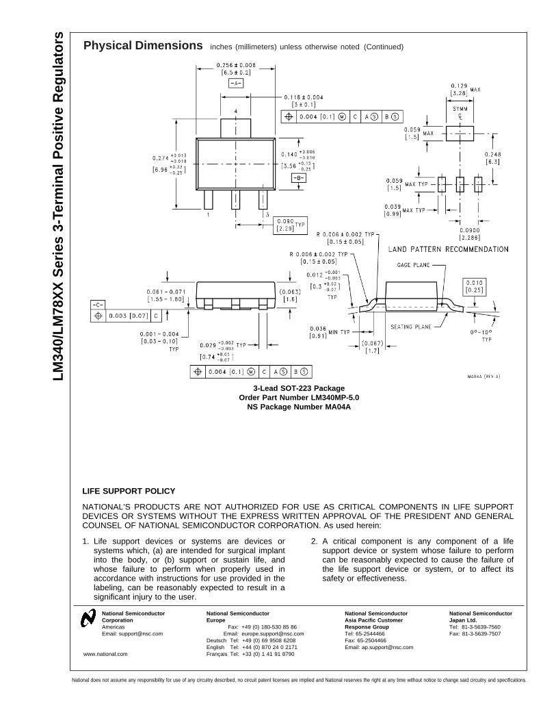
Physical Dimensions inches (millimeters) unless otherwise noted (Continued)
3-Lead SOT-223 PackageOrder Part Number LM340MP-5.0
NS Package Number MA04A
LIFE SUPPORT POLICY
NATIONAL’S PRODUCTS ARE NOT AUTHORIZED FOR USE AS CRITICAL COMPONENTS IN LIFE SUPPORTDEVICES OR SYSTEMS WITHOUT THE EXPRESS WRITTEN APPROVAL OF THE PRESIDENT AND GENERALCOUNSEL OF NATIONAL SEMICONDUCTOR CORPORATION. As used herein:
1. Life support devices or systems are devices orsystems which, (a) are intended for surgical implantinto the body, or (b) support or sustain life, andwhose failure to perform when properly used inaccordance with instructions for use provided in thelabeling, can be reasonably expected to result in asignificant injury to the user.
2. A critical component is any component of a lifesupport device or system whose failure to performcan be reasonably expected to cause the failure ofthe life support device or system, or to affect itssafety or effectiveness.
National SemiconductorCorporationAmericasEmail: [email protected]
National SemiconductorEurope
Fax: +49 (0) 180-530 85 86Email: [email protected]
Deutsch Tel: +49 (0) 69 9508 6208English Tel: +44 (0) 870 24 0 2171Français Tel: +33 (0) 1 41 91 8790
National SemiconductorAsia Pacific CustomerResponse GroupTel: 65-2544466Fax: 65-2504466Email: [email protected]
National SemiconductorJapan Ltd.Tel: 81-3-5639-7560Fax: 81-3-5639-7507
www.national.com
LM34
0/LM
78X
XS
erie
s3-
Term
inal
Pos
itive
Reg
ulat
ors
National does not assume any responsibility for use of any circuitry described, no circuit patent licenses are implied and National reserves the right at any time without notice to change said circuitry and specifications.


![LM340, A Series MOTOROLA ANALOG IC DEVICE DATA 3 LM340–5.0 ELECTRICAL CHARACTERISTICS (Vin = 10 V, IO = 500 mA, TJ = Tlow to Thigh [Note 1], unless otherwise noted.) Characteristics](https://img.pdfslide.net/doc/110x75/5e89a025c703964db07d8133/lm340-a-series-motorola-analog-ic-device-data-3-lm340a50-electrical-characteristics.jpg)