Embed Size (px)
Citation preview
LM4128
Input OutputVREF
EN
GND
Enable
CIN COUT* *
VIN
LM4128, LM4128Q
www.ti.com SNVS475E –NOVEMBER 2006–REVISED APRIL 2013
LM4128/LM4128Q SOT-23 Precision Micropower Series Voltage ReferenceCheck for Samples: LM4128, LM4128Q
1FEATURES DESCRIPTIONIdeal for space critical applications, the LM4128
2• Output Voltage Initial Accuracy 0.1%precision voltage reference is available in the SOT-23
• Low Temperature Coefficient 75 ppm/°C surface-mount package. The LM4128’s advanced• Low Supply Current, 60 µA design eliminates the need for an external stabilizing
capacitor while ensuring stability with capacitive loads• Enable Pin Allowing a 3 µA Shutdown Modeup to 10 µF, thus making the LM4128 easy to use.• Up to 20 mA Output CurrentSeries references provide lower power consumption• Voltage Options 1.8V, 2.048V, 2.5V, 3.0V, 3.3V,than shunt references, since they do not have to idle4.096Vthe maximum possible load current under no load
• Custom Voltage Options Available (1.8V to conditions. This advantage, the low quiescent current4.096V) (60 µA), and the low dropout voltage (400 mV) make
the LM4128 ideal for battery-powered solutions.• VIN Range of VREF + 400 mV to 5.5V @10 mA• Stable with Low ESR Ceramic Capacitors The LM4128 is available in four grades (A, B, C, and
D) for greater flexibility. The best grade devices (A)• 5-Pin SOT-23 Packagehave an initial accuracy of 0.1% with ensured• −40°C to 125°C Junction Temperature Rangetemperature coefficient of 75 ppm/°C or less, while
• LM4128AQ/BQ/CQ/DQ are AEC-Q100 Grade 1 the lowest grade parts (D) have an initial accuracy ofQualified and are Manufactured on an 1.0% and a tempco of 100 ppm/°C.Automotive Grade Flow
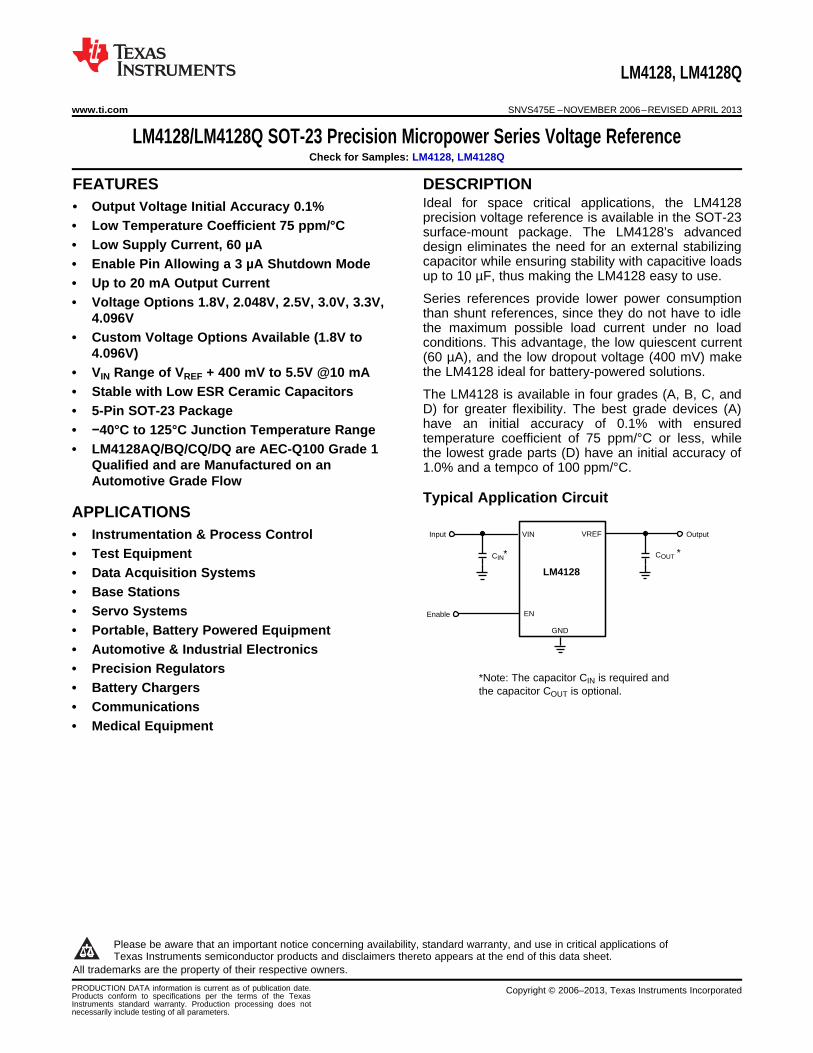
Typical Application CircuitAPPLICATIONS• Instrumentation & Process Control• Test Equipment• Data Acquisition Systems• Base Stations• Servo Systems• Portable, Battery Powered Equipment• Automotive & Industrial Electronics• Precision Regulators
*Note: The capacitor CIN is required and• Battery Chargers the capacitor COUT is optional.
• Communications• Medical Equipment
1
Please be aware that an important notice concerning availability, standard warranty, and use in critical applications ofTexas Instruments semiconductor products and disclaimers thereto appears at the end of this data sheet.
2All trademarks are the property of their respective owners.
PRODUCTION DATA information is current as of publication date. Copyright © 2006–2013, Texas Instruments IncorporatedProducts conform to specifications per the terms of the TexasInstruments standard warranty. Production processing does notnecessarily include testing of all parameters.
VIN
1
2
3
5
4EN
GND
N/C VREF
LM4128, LM4128Q
SNVS475E –NOVEMBER 2006–REVISED APRIL 2013 www.ti.com
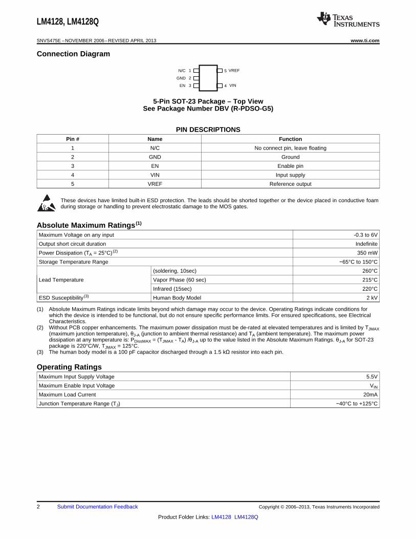
Connection Diagram
5-Pin SOT-23 Package – Top ViewSee Package Number DBV (R-PDSO-G5)
PIN DESCRIPTIONSPin # Name Function
1 N/C No connect pin, leave floating
2 GND Ground
3 EN Enable pin
4 VIN Input supply
5 VREF Reference output
These devices have limited built-in ESD protection. The leads should be shorted together or the device placed in conductive foamduring storage or handling to prevent electrostatic damage to the MOS gates.
Absolute Maximum Ratings (1)
Maximum Voltage on any input -0.3 to 6V
Output short circuit duration Indefinite
Power Dissipation (TA = 25°C) (2) 350 mW
Storage Temperature Range −65°C to 150°C
(soldering, 10sec) 260°C
Lead Temperature Vapor Phase (60 sec) 215°C
Infrared (15sec) 220°C
ESD Susceptibility (3) Human Body Model 2 kV
(1) Absolute Maximum Ratings indicate limits beyond which damage may occur to the device. Operating Ratings indicate conditions forwhich the device is intended to be functional, but do not ensure specific performance limits. For ensured specifications, see ElectricalCharacteristics.
(2) Without PCB copper enhancements. The maximum power dissipation must be de-rated at elevated temperatures and is limited by TJMAX(maximum junction temperature), θJ-A (junction to ambient thermal resistance) and TA (ambient temperature). The maximum powerdissipation at any temperature is: PDissMAX = (TJMAX - TA) /θJ-A up to the value listed in the Absolute Maximum Ratings. θJ-A for SOT-23package is 220°C/W, TJMAX = 125°C.
(3) The human body model is a 100 pF capacitor discharged through a 1.5 kΩ resistor into each pin.
Operating RatingsMaximum Input Supply Voltage 5.5V
Maximum Enable Input Voltage VIN
Maximum Load Current 20mA
Junction Temperature Range (TJ) −40°C to +125°C
2 Submit Documentation Feedback Copyright © 2006–2013, Texas Instruments Incorporated
Product Folder Links: LM4128 LM4128Q

LM4128, LM4128Q
www.ti.com SNVS475E –NOVEMBER 2006–REVISED APRIL 2013
Electrical CharacteristicsLM4128-1.8 (VOUT = 1.8V)Limits in standard type are for TJ = 25°C only, and limits in boldface type apply over the junction temperature (TJ) range of -40°C to +125°C unless otherwise specified. Minimum and Maximum limits are ensured through test, design, or statisticalcorrelation. Typical values represent the most likely parametric norm at TJ = 25°C, and are provided for reference purposesonly. Unless otherwise specified VIN = 5V and ILOAD = 0A.
Symbol Parameter Conditions Min (1) Typ (2) Max (1) Unit
VREF Output Voltage Initial Accuracy
LM4128A-1.8 (A Grade - 0.1%) -0.1 +0.1
LM4128B-1.8 (B Grade - 0.2%) -0.2 +0.2%
LM4128C-1.8 (C Grade - 0.5%) -0.5 +0.5
LM4128D-1.8 (D Grade - 1.0%) -1.0 +1.0
TCVREF / °C (3) LM4128A-1.8 75
LM4128B-1.8 75Temperature Coefficient ppm / °C
LM4128C-1.8 100
LM4128D-1.8 100
IQ Supply Current 60 100 µA
IQ_SD Supply Current in Shutdown EN = 0V 3 7 µA
ΔVREF/ΔVIN Line Regulation VREF + 400 mV ≤ VIN ≤ 5.5V 30 ppm / V
ΔVREF/ΔILOAD Load Regulation 0 mA ≤ ILOAD ≤ 20 mA 25 120 ppm / mA
ΔVREF Long Term Stability (4) 1000 Hrs 50ppm
Thermal Hysteresis (5) -40°C ≤ TJ ≤ +125°C 75
VIN - VREF Dropout Voltage (6) ILOAD = 10 mA 200 400 mV
VN Output Noise Voltage 0.1 Hz to 10 Hz 170 µVPP
ISC Short Circuit Current 75 mA
VIL Enable Pin Maximum Low Input Level 35 %V
VIH Enable Pin Minimum High Input Level 65 %V
(1) Limits are 100% production tested at 25°C. Limits over the operating temperature range are ensured through correlation using StatisticalQuality Control.
(2) Typical numbers are at 25°C and represent the most likely parametric norm.(3) Temperature coefficient is measured by the "Box" method; i.e., the maximum ΔVREF is divided by the maximum ΔT.(4) Long term stability is VREF @25°C measured during 1000 hrs.(5) Thermal hysteresis is defined as the change in +25°C output voltage before and after cycling the device from (-40°C to 125°C).(6) Dropout voltage is defined as the minimum input to output differential at which the output voltage drops by 0.5% below the value
measured with a 5V input.
Copyright © 2006–2013, Texas Instruments Incorporated Submit Documentation Feedback 3
Product Folder Links: LM4128 LM4128Q
LM4128, LM4128Q
SNVS475E –NOVEMBER 2006–REVISED APRIL 2013 www.ti.com
Electrical CharacteristicsLM4128-2.0 (VOUT = 2.048V)Limits in standard type are for TJ = 25°C only, and limits in boldface type apply over the junction temperature (TJ) range of -40°C to +125°C unless otherwise specified. Minimum and Maximum limits are ensured through test, design, or statisticalcorrelation. Typical values represent the most likely parametric norm at TJ = 25°C, and are provided for reference purposesonly. Unless otherwise specified VIN = 5V and ILOAD = 0A.
Symbol Parameter Conditions Min (1) Typ (2) Max (1) Unit
VREF Output Voltage Initial Accuracy
LM4128A-2.0 (A Grade - 0.1%) -0.1 +0.1
LM4128B-2.0 (B Grade - 0.2%) -0.2 +0.2%
LM4128C-2.0 (C Grade - 0.5%) -0.5 +0.5
LM4128D-2.0 (D Grade - 1.0%) -1.0 +1.0
TCVREF / °C (3) LM4128A-2.0 75
LM4128B-2.0 75Temperature Coefficient ppm / °C
LM4128C-2.0 100
LM4128D-2.0 100
IQ Supply Current 60 100 µA
IQ_SD Supply Current in Shutdown EN = 0V 3 7 µA
ΔVREF/ΔVIN Line Regulation VREF + 400 mV ≤ VIN ≤ 5.5V 30 ppm / V
ΔVREF/ΔILOAD Load Regulation 0 mA ≤ ILOAD ≤ 20 mA 25 120 ppm / mA
ΔVREF Long Term Stability (4) 1000 Hrs 50ppm
Thermal Hysteresis (5) -40°C ≤ TJ ≤ +125°C 75
VIN - VREF Dropout Voltage (6) ILOAD = 10 mA 175 400 mV
VN Output Noise Voltage 0.1 Hz to 10 Hz 190 µVPP
ISC Short Circuit Current 75 mA
VIL Enable Pin Maximum Low Input Level 35 %V
VIH Enable Pin Minimum High Input Level 65 %V
(1) Limits are 100% production tested at 25°C. Limits over the operating temperature range are ensured through correlation using StatisticalQuality Control.
(2) Typical numbers are at 25°C and represent the most likely parametric norm.(3) Temperature coefficient is measured by the "Box" method; i.e., the maximum ΔVREF is divided by the maximum ΔT.(4) Long term stability is VREF @25°C measured during 1000 hrs.(5) Thermal hysteresis is defined as the change in +25°C output voltage before and after cycling the device from (-40°C to 125°C).(6) Dropout voltage is defined as the minimum input to output differential at which the output voltage drops by 0.5% below the value
measured with a 5V input.
4 Submit Documentation Feedback Copyright © 2006–2013, Texas Instruments Incorporated
Product Folder Links: LM4128 LM4128Q
LM4128, LM4128Q
www.ti.com SNVS475E –NOVEMBER 2006–REVISED APRIL 2013
Electrical CharacteristicsLM4128-2.5 (VOUT = 2.5V)Limits in standard type are for TJ = 25°C only, and limits in boldface type apply over the junction temperature (TJ) range of -40°C to +125°C unless otherwise specified. Minimum and Maximum limits are ensured through test, design, or statisticalcorrelation. Typical values represent the most likely parametric norm at TJ = 25°C, and are provided for reference purposesonly. Unless otherwise specified VIN = 5V and ILOAD = 0A.
Symbol Parameter Conditions Min (1) Typ (2) Max (1) Unit
VREF Output Voltage Initial Accuracy
LM4128A-2.5 (A Grade - 0.1%) -0.1 +0.1
LM4128B-2.5 (B Grade - 0.2%) -0.2 +0.2%
LM4128C-2.5 (C Grade - 0.5%) -0.5 +0.5
LM4128D-2.5 (D Grade - 1.0%) -1.0 +1.0
TCVREF / °C (3) LM4128A-2.5 75
LM4128B-2.5 75Temperature Coefficient ppm / °C
LM4128C-2.5 100
LM4128D-2.5 100
IQ Supply Current 60 100 µA
IQ_SD Supply Current in Shutdown EN = 0V 3 7 µA
ΔVREF/ΔVIN Line Regulation VREF + 400 mV ≤ VIN ≤ 5.5V 50 ppm / V
ΔVREF/ΔILOAD Load Regulation 0 mA ≤ ILOAD ≤ 20 mA 25 120 ppm / mA
ΔVREF Long Term Stability (4) 1000 Hrs 50ppm
Thermal Hysteresis (5) -40°C ≤ TJ ≤ +125°C 75
VIN - VREF Dropout Voltage (6) ILOAD = 10 mA 175 400 mV
VN Output Noise Voltage 0.1 Hz to 10 Hz 275 µVPP
ISC Short Circuit Current 75 mA
VIL Enable Pin Maximum Low Input Level 35 %V
VIH Enable Pin Minimum High Input Level 65 %V
(1) Limits are 100% production tested at 25°C. Limits over the operating temperature range are ensured through correlation using StatisticalQuality Control.
(2) Typical numbers are at 25°C and represent the most likely parametric norm.(3) Temperature coefficient is measured by the "Box" method; i.e., the maximum ΔVREF is divided by the maximum ΔT.(4) Long term stability is VREF @25°C measured during 1000 hrs.(5) Thermal hysteresis is defined as the change in +25°C output voltage before and after cycling the device from (-40°C to 125°C).(6) Dropout voltage is defined as the minimum input to output differential at which the output voltage drops by 0.5% below the value
measured with a 5V input.
Copyright © 2006–2013, Texas Instruments Incorporated Submit Documentation Feedback 5
Product Folder Links: LM4128 LM4128Q
LM4128, LM4128Q
SNVS475E –NOVEMBER 2006–REVISED APRIL 2013 www.ti.com
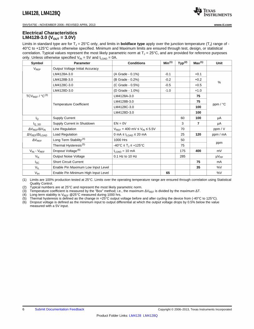
Electrical CharacteristicsLM4128-3.0 (VOUT = 3.0V)Limits in standard type are for TJ = 25°C only, and limits in boldface type apply over the junction temperature (TJ) range of -40°C to +125°C unless otherwise specified. Minimum and Maximum limits are ensured through test, design, or statisticalcorrelation. Typical values represent the most likely parametric norm at TJ = 25°C, and are provided for reference purposesonly. Unless otherwise specified VIN = 5V and ILOAD = 0A.
Symbol Parameter Conditions Min (1) Typ (2) Max (1) Unit
VREF Output Voltage Initial Accuracy
LM4128A-3.0 (A Grade - 0.1%) -0.1 +0.1
LM4128B-3.0 (B Grade - 0.2%) -0.2 +0.2%
LM4128C-3.0 (C Grade - 0.5%) -0.5 +0.5
LM4128D-3.0 (D Grade - 1.0%) -1.0 +1.0
TCVREF / °C (3) LM4128A-3.0 75
LM4128B-3.0 75Temperature Coefficient ppm / °C
LM4128C-3.0 100
LM4128D-3.0 100
IQ Supply Current 60 100 µA
IQ_SD Supply Current in Shutdown EN = 0V 3 7 µA
ΔVREF/ΔVIN Line Regulation VREF + 400 mV ≤ VIN ≤ 5.5V 70 ppm / V
ΔVREF/ΔILOAD Load Regulation 0 mA ≤ ILOAD ≤ 20 mA 25 120 ppm / mA
ΔVREF Long Term Stability (4) 1000 Hrs 50ppm
Thermal Hysteresis (5) -40°C ≤ TJ ≤ +125°C 75
VIN - VREF Dropout Voltage (6) ILOAD = 10 mA 175 400 mV
VN Output Noise Voltage 0.1 Hz to 10 Hz 285 µVPP
ISC Short Circuit Current 75 mA
VIL Enable Pin Maximum Low Input Level 35 %V
VIH Enable Pin Minimum High Input Level 65 %V
(1) Limits are 100% production tested at 25°C. Limits over the operating temperature range are ensured through correlation using StatisticalQuality Control.
(2) Typical numbers are at 25°C and represent the most likely parametric norm.(3) Temperature coefficient is measured by the "Box" method; i.e., the maximum ΔVREF is divided by the maximum ΔT.(4) Long term stability is VREF @25°C measured during 1000 hrs.(5) Thermal hysteresis is defined as the change in +25°C output voltage before and after cycling the device from (-40°C to 125°C).(6) Dropout voltage is defined as the minimum input to output differential at which the output voltage drops by 0.5% below the value
measured with a 5V input.
6 Submit Documentation Feedback Copyright © 2006–2013, Texas Instruments Incorporated
Product Folder Links: LM4128 LM4128Q

LM4128, LM4128Q
www.ti.com SNVS475E –NOVEMBER 2006–REVISED APRIL 2013
Electrical CharacteristicsLM4128-3.3 (VOUT = 3.3V)Limits in standard type are for TJ = 25°C only, and limits in boldface type apply over the junction temperature (TJ) range of -40°C to +125°C unless otherwise specified. Minimum and Maximum limits are ensured through test, design, or statisticalcorrelation. Typical values represent the most likely parametric norm at TJ = 25°C, and are provided for reference purposesonly. Unless otherwise specified VIN = 5V and ILOAD = 0A.
Symbol Parameter Conditions Min (1) Typ (2) Max (1) Unit
VREF Output Voltage Initial Accuracy
LM4128A-3.3 (A Grade - 0.1%) -0.1 +0.1
LM4128B-3.3 (B Grade - 0.2%) -0.2 +0.2%
LM4128C-3.3 (C Grade - 0.5%) -0.5 +0.5
LM4128D-3.3 (D Grade - 1.0%) -1.0 +1.0
TCVREF / °C (3) LM4128A-3.3 75
LM4128B-3.3 75Temperature Coefficient ppm / °C
LM4128C-3.3 100
LM4128D-3.3 100
IQ Supply Current 60 100 µA
IQ_SD Supply Current in Shutdown EN = 0V 3 7 µA
ΔVREF/ΔVIN Line Regulation VREF + 400 mV ≤ VIN ≤ 5.5V 85 ppm / V
ΔVREF/ΔILOAD Load Regulation 0 mA ≤ ILOAD ≤ 20 mA 25 120 ppm / mA
ΔVREF Long Term Stability (4) 1000 Hrs 50ppm
Thermal Hysteresis (5) -40°C ≤ TJ ≤ +125°C 75
VIN - VREF Dropout Voltage (6) ILOAD = 10 mA 175 400 mV
VN Output Noise Voltage 0.1 Hz to 10 Hz 310 µVPP
ISC Short Circuit Current 75 mA
VIL Enable Pin Maximum Low Input Level 35 %V
VIH Enable Pin Minimum High Input Level 65 %V
(1) Limits are 100% production tested at 25°C. Limits over the operating temperature range are ensured through correlation using StatisticalQuality Control.
(2) Typical numbers are at 25°C and represent the most likely parametric norm.(3) Temperature coefficient is measured by the "Box" method; i.e., the maximum ΔVREF is divided by the maximum ΔT.(4) Long term stability is VREF @25°C measured during 1000 hrs.(5) Thermal hysteresis is defined as the change in +25°C output voltage before and after cycling the device from (-40°C to 125°C).(6) Dropout voltage is defined as the minimum input to output differential at which the output voltage drops by 0.5% below the value
measured with a 5V input.
Copyright © 2006–2013, Texas Instruments Incorporated Submit Documentation Feedback 7
Product Folder Links: LM4128 LM4128Q

LM4128, LM4128Q
SNVS475E –NOVEMBER 2006–REVISED APRIL 2013 www.ti.com
Electrical CharacteristicsLM4128-4.1 (VOUT = 4.096V)Limits in standard type are for TJ = 25°C only, and limits in boldface type apply over the junction temperature (TJ) range of -40°C to +125°C unless otherwise specified. Minimum and Maximum limits are ensured through test, design, or statisticalcorrelation. Typical values represent the most likely parametric norm at TJ = 25°C, and are provided for reference purposesonly. Unless otherwise specified VIN = 5V and ILOAD = 0A.
Symbol Parameter Conditions Min (1) Typ (2) Max (1) Unit
VREF Output Voltage Initial Accuracy
LM4128A-4.1 (A Grade - 0.1%) -0.1 +0.1
LM4128B-4.1 (B Grade - 0.2%) -0.2 +0.2%
LM4128C-4.1 (C Grade - 0.5%) -0.5 +0.5
LM4128D-4.1 (D Grade - 1.0%) -1.0 +1.0
TCVREF / °C (3) LM4128A-4.1 75
LM4128B-4.1 75Temperature Coefficient ppm / °C
LM4128C-4.1 100
LM4128D-4.1 100
IQ Supply Current 60 100 µA
IQ_SD Supply Current in Shutdown EN = 0V 3 7 µA
ΔVREF/ΔVIN Line Regulation VREF + 400 mV ≤ VIN ≤ 5.5V 100 ppm / V
ΔVREF/ΔILOAD Load Regulation 0 mA ≤ ILOAD ≤ 20 mA 25 120 ppm / mA
ΔVREF Long Term Stability (4) 1000 Hrs 50ppm
Thermal Hysteresis (5) -40°C ≤ TJ ≤ +125°C 75
VIN - VREF Dropout Voltage (6) ILOAD = 10 mA 175 400 mV
VN Output Noise Voltage 0.1 Hz to 10 Hz 350 µVPP
ISC Short Circuit Current 75 mA
VIL Enable Pin Maximum Low Input Level 35 %V
VIH Enable Pin Minimum High Input Level 65 %V
(1) Limits are 100% production tested at 25°C. Limits over the operating temperature range are ensured through correlation using StatisticalQuality Control.
(2) Typical numbers are at 25°C and represent the most likely parametric norm.(3) Temperature coefficient is measured by the "Box" method; i.e., the maximum ΔVREF is divided by the maximum ΔT.(4) Long term stability is VREF @25°C measured during 1000 hrs.(5) Thermal hysteresis is defined as the change in +25°C output voltage before and after cycling the device from (-40°C to 125°C).(6) Dropout voltage is defined as the minimum input to output differential at which the output voltage drops by 0.5% below the value
measured with a 5V input.
8 Submit Documentation Feedback Copyright © 2006–2013, Texas Instruments Incorporated
Product Folder Links: LM4128 LM4128Q
10 100 1000 10000
FREQUENCY (Hz)
OU
TP
UT
NO
ISE
VO
LTA
GE
(P
Vrm
s/rt
(Hz)
)
4.096V
3.3V
3.0V
2.5V
2.0V
1.8V
0
5
10
15
20
25
30
35
10 100 1k 10k 100k 1M0
90
PO
WE
R S
UP
PLY
RE
JEC
TIO
N R
AT
IO (
dB)
FREQUENCY (Hz)
10
20
30
40
50
60
70
80
COUT = 1 PF
No COUT
C OU
T =
0.1
PF
3.0 3.5 4.0 4.5 5.0 5.52.497
2.498
2.499
2.500
2.501
2.502
OU
TP
UT
VO
LTA
GE
(V
)
INPUT VOLTAGE (V)
125°C
25°C
-40°C
-40 -20 0 20 40 60 80 100 120
TEMPERATURE (oC)
2.4925
2.495
2.4975
2.5
2.5025
2.505
2.5075
OU
TP
UT
VO
LTA
GE
(V
) 5 Typical Units
1 10 100 1000 10000 100000
OU
TP
UT
VO
LTA
GE
(V
)
LOAD CURRENT (PA)
2.496
2.497
2.498
2.499
2.500
2.501
2.502
2.503
2.504
2.505
2.506
-40°C
25°C
125°C
LM4128, LM4128Q
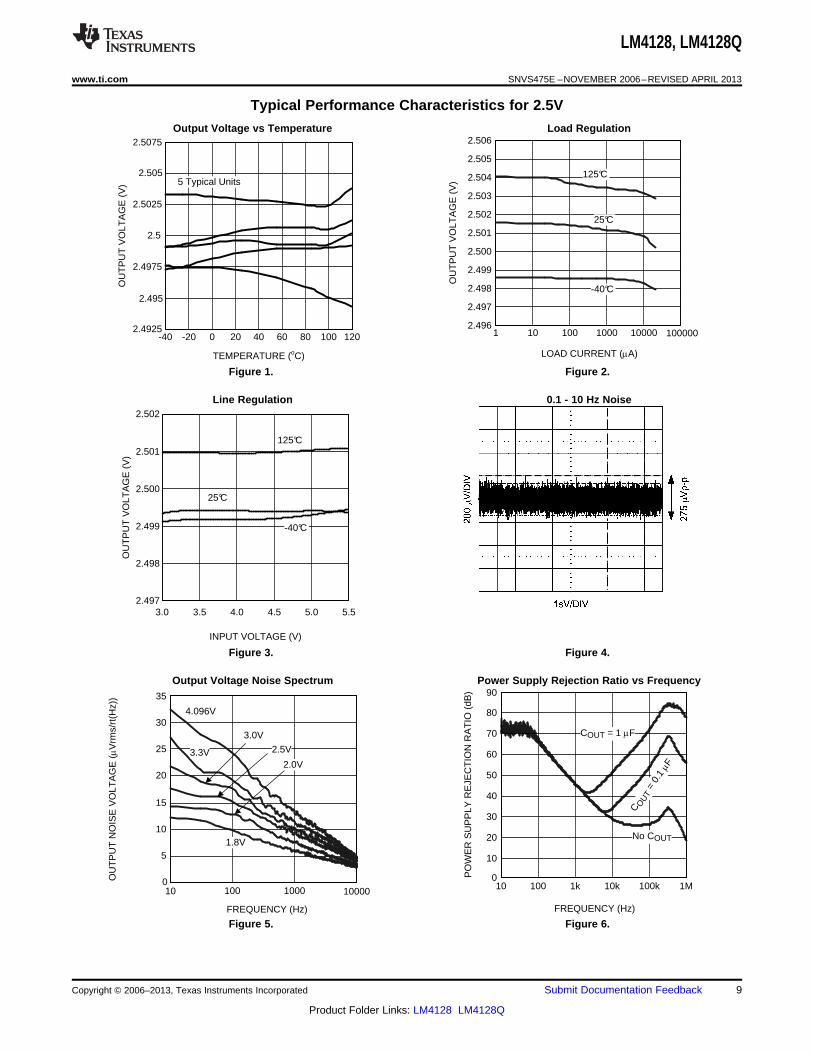
www.ti.com SNVS475E –NOVEMBER 2006–REVISED APRIL 2013
Typical Performance Characteristics for 2.5V
Output Voltage vs Temperature Load Regulation
Figure 1. Figure 2.
Line Regulation 0.1 - 10 Hz Noise
Figure 3. Figure 4.
Output Voltage Noise Spectrum Power Supply Rejection Ratio vs Frequency
Figure 5. Figure 6.
Copyright © 2006–2013, Texas Instruments Incorporated Submit Documentation Feedback 9
Product Folder Links: LM4128 LM4128Q
0 200
10
20
30
40
50
60
70
80
90
100
GR
OU
ND
CU
RR
EN
T (P
A)
LOAD CURRENT (mA)
5 10 15
125oC
25oC
-40oC
2.0 2.5 3.0 3.5 4.0 4.5 5.0
INPUT VOLTAGE (V)
2.0
2.5
3.0
3.5
4.0
4.5
5.0
SH
UT
DO
WN
I Q (P
A) 125°C
25°C
-40°C
5.50 1 2 3 4 50
10
20
30
40
50
60
70
80
90
100
SU
PP
LY C
UR
RE
NT
(P
A)
INPUT VOLTAGE (V)
0 200 400 600 800 1000-200
-150
-100
-50
0
50
100
150
200
DR
IFT
(pp
m)
TIME (Hours)
1 TYPICAL UNIT FROM EACHVOLTAGE OPTION
0 5 10 15 200
600V
DR
OP
OU
T (
mV
)
LOAD CURRENT (mA)
200
400
125°
C
25°C
-40°C
LM4128, LM4128Q
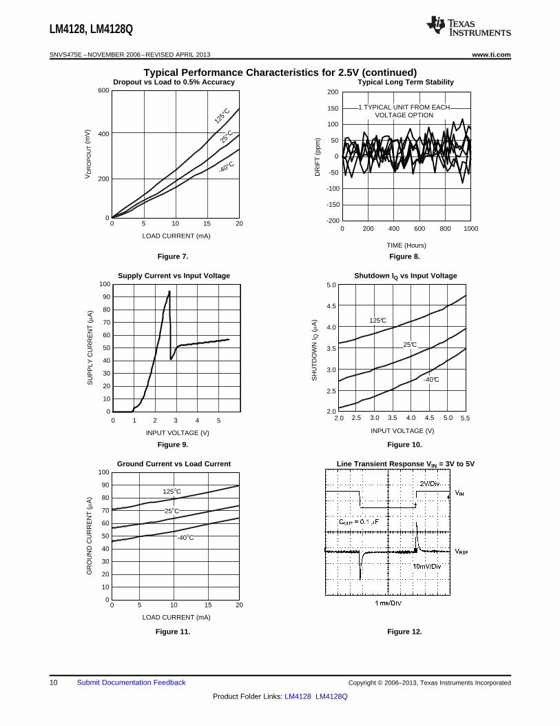
SNVS475E –NOVEMBER 2006–REVISED APRIL 2013 www.ti.com
Typical Performance Characteristics for 2.5V (continued)Dropout vs Load to 0.5% Accuracy Typical Long Term Stability
Figure 7. Figure 8.
Supply Current vs Input Voltage Shutdown IQ vs Input Voltage
Figure 9. Figure 10.
Ground Current vs Load Current Line Transient Response VIN = 3V to 5V
Figure 11. Figure 12.
10 Submit Documentation Feedback Copyright © 2006–2013, Texas Instruments Incorporated
Product Folder Links: LM4128 LM4128Q
LM4128, LM4128Q
www.ti.com SNVS475E –NOVEMBER 2006–REVISED APRIL 2013
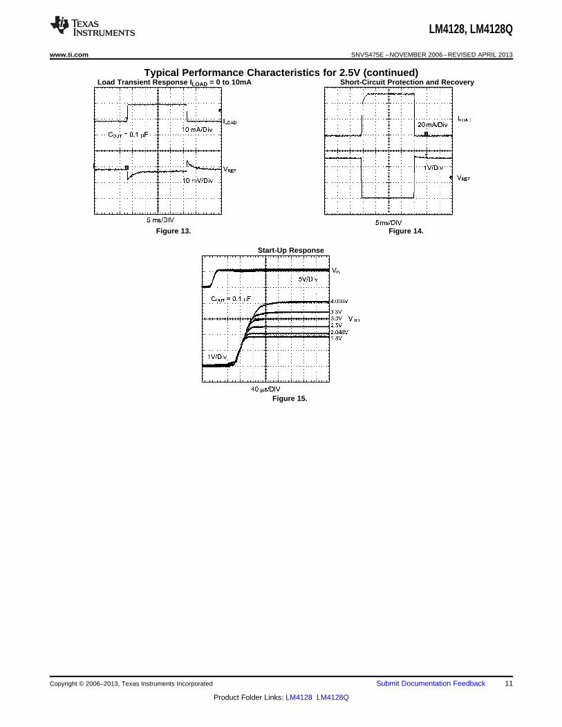
Typical Performance Characteristics for 2.5V (continued)Load Transient Response ILOAD = 0 to 10mA Short-Circuit Protection and Recovery
Figure 13. Figure 14.
Start-Up Response
Figure 15.
Copyright © 2006–2013, Texas Instruments Incorporated Submit Documentation Feedback 11
Product Folder Links: LM4128 LM4128Q
LM4128, LM4128Q
SNVS475E –NOVEMBER 2006–REVISED APRIL 2013 www.ti.com
APPLICATION INFORMATION
THEORY OF OPERATION
The foundation of any voltage reference is the band-gap circuit. While the reference in the LM4128 is developedfrom the gate-source voltage of transistors in the IC, principles of the band-gap circuit are easily understoodusing a bipolar example. For a detailed analysis of the bipolar band-gap circuit, see the AN-56 Application Report(SNVA514).
SUPPLY AND ENABLE VOLTAGES
To ensure proper operation, VEN and VIN must be within a specified range. An acceptable range of input voltagesis
VIN > VREF + 400 mV (ILOAD ≤ 10 mA) (1)
The enable pin uses an internal pull-up current source (IPULL_UP ≊ 2 µA) that may be left floating or triggered byan external source. If the part is not enabled by an external source, it may be connected to VIN. An acceptablerange of enable voltages is given by the enable transfer characteristics. See the Electrical Characteristics sectionand Enable Transfer Characteristics figure for more detail. Note, the part will not operate correctly for VEN > VIN.
COMPONENT SELECTION
A small ceramic (X5R or X7R) capacitor on the input must be used to ensure stable operation. The value of CINmust be sized according to the output capacitor value. The value of CIN must satisfy the relationship CIN ≥ COUT.When no output capacitor is used, CIN must have a minimum value of 0.1 µF. Noise on the power-supply inputmay affect the output noise. Larger input capacitor values (typically 4.7 µF to 22 µF) may help reduce noise onthe output and significantly reduce overshoot during startup. Use of an additional optional bypass capacitorbetween the input and ground may help further reduce noise on the output. With an input capacitor, the LM4128will drive any combination of resistance and capacitance up to VREF/20 mA and 10 µF respectively.
The LM4128 is designed to operate with or without an output capacitor and is stable with capacitive loads up to10 µF. Connecting a capacitor between the output and ground will significantly improve the load transientresponse when switching from a light load to a heavy load. The output capacitor should not be made arbitrarilylarge because it will effect the turn-on time as well as line and load transients.
While a variety of capacitor chemistry types may be used, it is typically advisable to use low esr ceramiccapacitors. Such capacitors provide a low impedance to high frequency signals, effectively bypassing them toground. Bypass capacitors should be mounted close to the part. Mounting bypass capacitors close to the part willhelp reduce the parasitic trace components thereby improving performance.
SHORT CIRCUITED OUTPUT
The LM4128 features indefinite short circuit protection. This protection limits the output current to 75 mA whenthe output is shorted to ground.
TURN ON TIME
Turn on time is defined as the time taken for the output voltage to rise to 90% of the preset value. The turn ontime depends on the load. The turn on time is typically 33.2 µs when driving a 1µF load and 78.8 µs when drivinga 10 µF load. Some users may experience an extended turn on time (up to 10 ms) under brown out conditionsand low temperatures (-40°C).
THERMAL HYSTERESIS
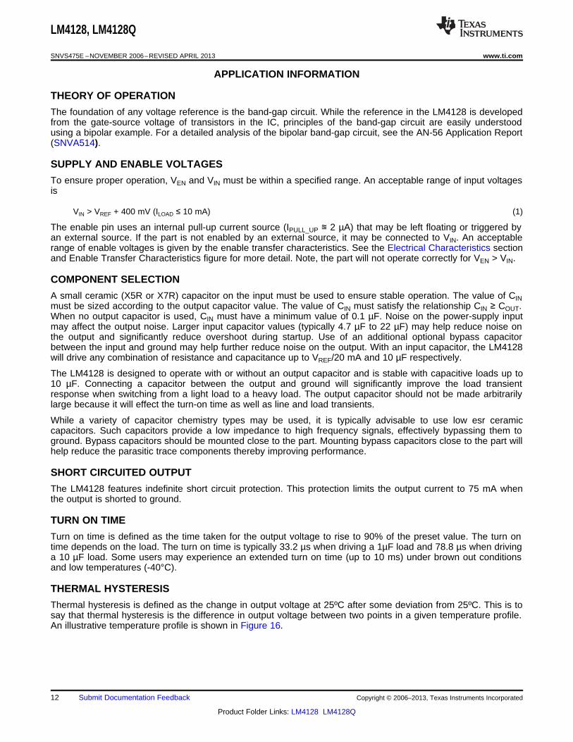
Thermal hysteresis is defined as the change in output voltage at 25ºC after some deviation from 25ºC. This is tosay that thermal hysteresis is the difference in output voltage between two points in a given temperature profile.An illustrative temperature profile is shown in Figure 16.
12 Submit Documentation Feedback Copyright © 2006–2013, Texas Instruments Incorporated
Product Folder Links: LM4128 LM4128Q
Temperature Range
Voltage
Temperature
VREF_MAX
Cha
nge
in O
utpu
t Vol
tage
VREF_MIN
VHYS =lVREF1 - VREF2l
VREFx 103 mV
-40°C
VREF1
Time
VREF2
25°C
125°C
LM4128, LM4128Q
www.ti.com SNVS475E –NOVEMBER 2006–REVISED APRIL 2013
Figure 16. Illustrative Temperature Profile
This may be expressed analytically as the following:
where• VHYS = Thermal hysteresis expressed in ppm• VREF = Nominal preset output voltage• VREF1 = VREF before temperature fluctuation• VREF2 = VREF after temperature fluctuation (2)
The LM4128 features a low thermal hysteresis of 190 µV from -40°C to 125°C.
TEMPERATURE COEFFICIENT
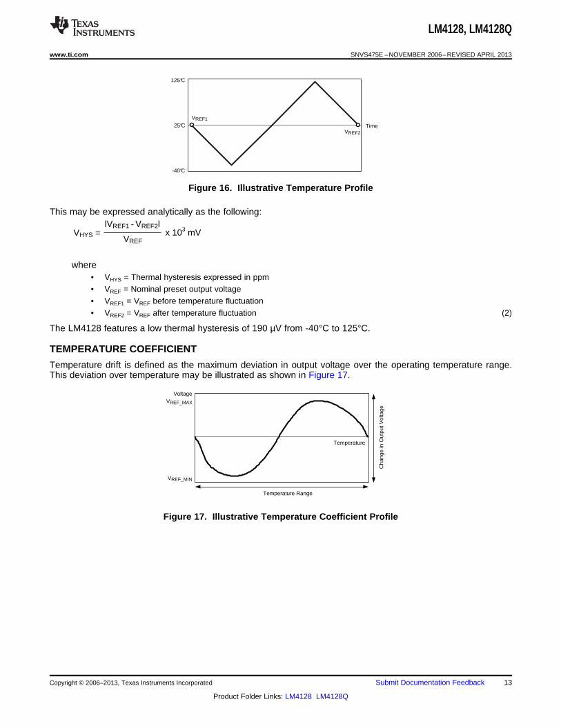
Temperature drift is defined as the maximum deviation in output voltage over the operating temperature range.This deviation over temperature may be illustrated as shown in Figure 17.
Figure 17. Illustrative Temperature Coefficient Profile
Copyright © 2006–2013, Texas Instruments Incorporated Submit Documentation Feedback 13
Product Folder Links: LM4128 LM4128Q
x 0.1VREF
= Percent_ErrorVERROR
x 103
VREF= ppmERROR
VERROR
x 103VREF
2n = VERROR
= VERROR103
VREF x ppmERROR
TD =VREF x 'T
x 106 ppm(VREF_MAX - VREF_MIN)
LM4128, LM4128Q
SNVS475E –NOVEMBER 2006–REVISED APRIL 2013 www.ti.com
Temperature coefficient may be expressed analytically as the following:
where• TD = Temperature drift• VREF = Nominal preset output voltage• VREF_MIN = Minimum output voltage over operating temperature range• VREF_MAX = Maximum output voltage over operating temperature range• ΔT = Operating temperature range (3)
The LM4128 features a low temperature drift of 75 ppm (max) to 100 ppm (max), depending on the grade, from -40°C to 125°C.
LONG TERM STABILITY
Long-term stability refers to the fluctuation in output voltage over a long period of time (1000 hours). The LM4128features a typical long-term stability of 50 ppm over 1000 hours. The measurements are made using 5 units ofeach voltage option, at a nominal input voltage (5V), with no load, at room temperature.
EXPRESSION OF ELECTRICAL CHARACTERISTICS
Electrical characteristics are typically expressed in mV, ppm, or a percentage of the nominal value. Dependingon the application, one expression may be more useful than the other. To convert one quantity to the other onemay apply the following:
ppm to mV error in output voltage:
where• VREF is in volts (V) and VERROR is in milli-volts (mV) (4)
Bit error (1 bit) to voltage error (mV):
where• VREF is in volts (V)• VERROR is in milli-volts (mV)• and n is the number of bits (5)
mV to ppm error in output voltage:
where• VREF is in volts (V)• VERROR is in milli-volts (mV) (6)
Voltage error (mV) to percentage error (percent):
where• VREF is in volts (V)• VERROR is in milli-volts (mV) (7)
14 Submit Documentation Feedback Copyright © 2006–2013, Texas Instruments Incorporated
Product Folder Links: LM4128 LM4128Q
LM4128
VIN
ENGND
VREFInput
Enable
Output
CIN
R1500 :
RSET
1 k:
IOUT
R L
0.1 µF
IGNDIOUT = (VREF/(R1 + RSET)) + IGND
LM4128
VIN
ENGND
VREFInput
Enable
+5V
100 k:
0.1 µF
V
V
REF_FORCE
REF_SENSE
CIN
LM4128
VIN
ENGND
VREFInput
Enable
VREF
CIN COUTR
R
R/2
-VREF
+5V
-5V
4.7 µF < C OUT < 10 µF
LM4128, LM4128Q
www.ti.com SNVS475E –NOVEMBER 2006–REVISED APRIL 2013
PRINTED CIRCUIT BOARD and LAYOUT CONSIDERATIONS
References in SOT packages are generally less prone to PC board mounting than devices in Small Outline(SOIC) packages. To minimize the mechanical stress due to PC board mounting that can cause the outputvoltage to shift from its initial value, mount the reference on a low flex area of the PC board, such as near theedge or a corner.
The part may be isolated mechanically by cutting a U shape slot on the PCB for mounting the device. Thisapproach also provides some thermal isolation from the rest of the circuit.
Bypass capacitors must be mounted close to the part. Mounting bypass capacitors close to the part will reducethe parasitic trace components thereby improving performance.
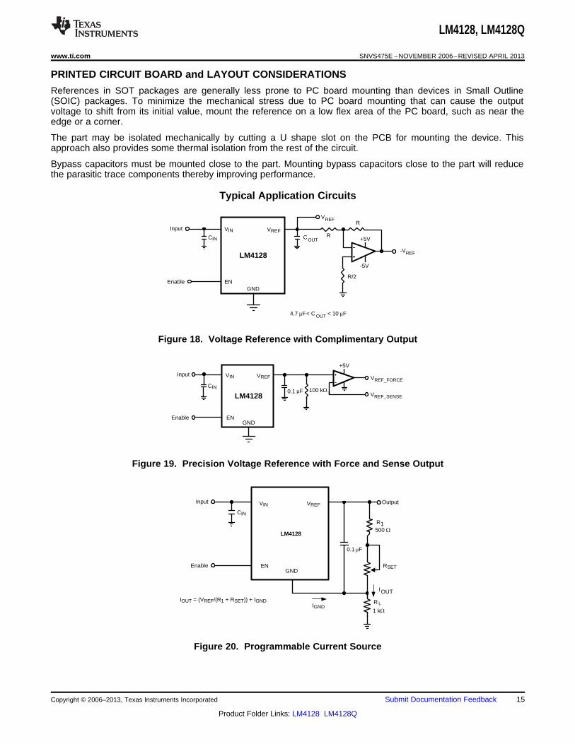
Typical Application Circuits
Figure 18. Voltage Reference with Complimentary Output
Figure 19. Precision Voltage Reference with Force and Sense Output
Figure 20. Programmable Current Source
Copyright © 2006–2013, Texas Instruments Incorporated Submit Documentation Feedback 15
Product Folder Links: LM4128 LM4128Q
LM4128, LM4128Q
SNVS475E –NOVEMBER 2006–REVISED APRIL 2013 www.ti.com
REVISION HISTORY
Changes from Revision D (April 2013) to Revision E Page
• Changed layout of National Data Sheet to TI format .......................................................................................................... 15
16 Submit Documentation Feedback Copyright © 2006–2013, Texas Instruments Incorporated
Product Folder Links: LM4128 LM4128Q
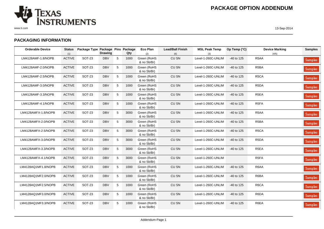
PACKAGE OPTION ADDENDUM
www.ti.com 13-Sep-2014
Addendum-Page 1
PACKAGING INFORMATION
Orderable Device Status(1)
Package Type PackageDrawing
Pins PackageQty
Eco Plan(2)
Lead/Ball Finish(6)
MSL Peak Temp(3)
Op Temp (°C) Device Marking(4/5)
Samples
LM4128AMF-1.8/NOPB ACTIVE SOT-23 DBV 5 1000 Green (RoHS& no Sb/Br)
CU SN Level-1-260C-UNLIM -40 to 125 R5AA
LM4128AMF-2.0/NOPB ACTIVE SOT-23 DBV 5 1000 Green (RoHS& no Sb/Br)
CU SN Level-1-260C-UNLIM -40 to 125 R5BA
LM4128AMF-2.5/NOPB ACTIVE SOT-23 DBV 5 1000 Green (RoHS& no Sb/Br)
CU SN Level-1-260C-UNLIM -40 to 125 R5CA
LM4128AMF-3.0/NOPB ACTIVE SOT-23 DBV 5 1000 Green (RoHS& no Sb/Br)
CU SN Level-1-260C-UNLIM -40 to 125 R5DA
LM4128AMF-3.3/NOPB ACTIVE SOT-23 DBV 5 1000 Green (RoHS& no Sb/Br)
CU SN Level-1-260C-UNLIM -40 to 125 R5EA
LM4128AMF-4.1/NOPB ACTIVE SOT-23 DBV 5 1000 Green (RoHS& no Sb/Br)
CU SN Level-1-260C-UNLIM -40 to 125 R5FA
LM4128AMFX-1.8/NOPB ACTIVE SOT-23 DBV 5 3000 Green (RoHS& no Sb/Br)
CU SN Level-1-260C-UNLIM -40 to 125 R5AA
LM4128AMFX-2.0/NOPB ACTIVE SOT-23 DBV 5 3000 Green (RoHS& no Sb/Br)
CU SN Level-1-260C-UNLIM -40 to 125 R5BA
LM4128AMFX-2.5/NOPB ACTIVE SOT-23 DBV 5 3000 Green (RoHS& no Sb/Br)
CU SN Level-1-260C-UNLIM -40 to 125 R5CA
LM4128AMFX-3.0/NOPB ACTIVE SOT-23 DBV 5 3000 Green (RoHS& no Sb/Br)
CU SN Level-1-260C-UNLIM -40 to 125 R5DA
LM4128AMFX-3.3/NOPB ACTIVE SOT-23 DBV 5 3000 Green (RoHS& no Sb/Br)
CU SN Level-1-260C-UNLIM -40 to 125 R5EA
LM4128AMFX-4.1/NOPB ACTIVE SOT-23 DBV 5 3000 Green (RoHS& no Sb/Br)
CU SN Level-1-260C-UNLIM R5FA
LM4128AQ1MF1.8/NOPB ACTIVE SOT-23 DBV 5 1000 Green (RoHS& no Sb/Br)
CU SN Level-1-260C-UNLIM -40 to 125 R6AA
LM4128AQ1MF2.0/NOPB ACTIVE SOT-23 DBV 5 1000 Green (RoHS& no Sb/Br)
CU SN Level-1-260C-UNLIM -40 to 125 R6BA
LM4128AQ1MF2.5/NOPB ACTIVE SOT-23 DBV 5 1000 Green (RoHS& no Sb/Br)
CU SN Level-1-260C-UNLIM -40 to 125 R6CA
LM4128AQ1MF3.0/NOPB ACTIVE SOT-23 DBV 5 1000 Green (RoHS& no Sb/Br)
CU SN Level-1-260C-UNLIM -40 to 125 R6DA
LM4128AQ1MF3.3/NOPB ACTIVE SOT-23 DBV 5 1000 Green (RoHS& no Sb/Br)
CU SN Level-1-260C-UNLIM -40 to 125 R6EA
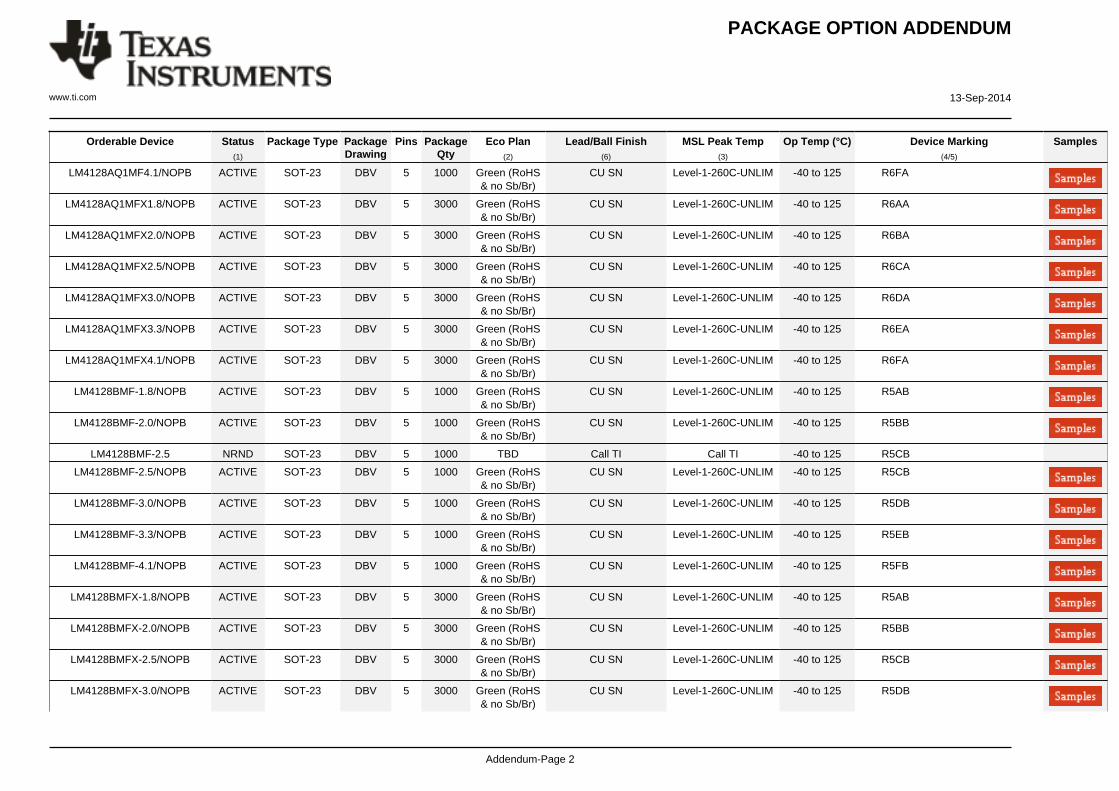
PACKAGE OPTION ADDENDUM
www.ti.com 13-Sep-2014
Addendum-Page 2
Orderable Device Status(1)
Package Type PackageDrawing
Pins PackageQty
Eco Plan(2)
Lead/Ball Finish(6)
MSL Peak Temp(3)
Op Temp (°C) Device Marking(4/5)
Samples
LM4128AQ1MF4.1/NOPB ACTIVE SOT-23 DBV 5 1000 Green (RoHS& no Sb/Br)
CU SN Level-1-260C-UNLIM -40 to 125 R6FA
LM4128AQ1MFX1.8/NOPB ACTIVE SOT-23 DBV 5 3000 Green (RoHS& no Sb/Br)
CU SN Level-1-260C-UNLIM -40 to 125 R6AA
LM4128AQ1MFX2.0/NOPB ACTIVE SOT-23 DBV 5 3000 Green (RoHS& no Sb/Br)
CU SN Level-1-260C-UNLIM -40 to 125 R6BA
LM4128AQ1MFX2.5/NOPB ACTIVE SOT-23 DBV 5 3000 Green (RoHS& no Sb/Br)
CU SN Level-1-260C-UNLIM -40 to 125 R6CA
LM4128AQ1MFX3.0/NOPB ACTIVE SOT-23 DBV 5 3000 Green (RoHS& no Sb/Br)
CU SN Level-1-260C-UNLIM -40 to 125 R6DA
LM4128AQ1MFX3.3/NOPB ACTIVE SOT-23 DBV 5 3000 Green (RoHS& no Sb/Br)
CU SN Level-1-260C-UNLIM -40 to 125 R6EA
LM4128AQ1MFX4.1/NOPB ACTIVE SOT-23 DBV 5 3000 Green (RoHS& no Sb/Br)
CU SN Level-1-260C-UNLIM -40 to 125 R6FA
LM4128BMF-1.8/NOPB ACTIVE SOT-23 DBV 5 1000 Green (RoHS& no Sb/Br)
CU SN Level-1-260C-UNLIM -40 to 125 R5AB
LM4128BMF-2.0/NOPB ACTIVE SOT-23 DBV 5 1000 Green (RoHS& no Sb/Br)
CU SN Level-1-260C-UNLIM -40 to 125 R5BB
LM4128BMF-2.5 NRND SOT-23 DBV 5 1000 TBD Call TI Call TI -40 to 125 R5CB
LM4128BMF-2.5/NOPB ACTIVE SOT-23 DBV 5 1000 Green (RoHS& no Sb/Br)
CU SN Level-1-260C-UNLIM -40 to 125 R5CB
LM4128BMF-3.0/NOPB ACTIVE SOT-23 DBV 5 1000 Green (RoHS& no Sb/Br)
CU SN Level-1-260C-UNLIM -40 to 125 R5DB
LM4128BMF-3.3/NOPB ACTIVE SOT-23 DBV 5 1000 Green (RoHS& no Sb/Br)
CU SN Level-1-260C-UNLIM -40 to 125 R5EB
LM4128BMF-4.1/NOPB ACTIVE SOT-23 DBV 5 1000 Green (RoHS& no Sb/Br)
CU SN Level-1-260C-UNLIM -40 to 125 R5FB
LM4128BMFX-1.8/NOPB ACTIVE SOT-23 DBV 5 3000 Green (RoHS& no Sb/Br)
CU SN Level-1-260C-UNLIM -40 to 125 R5AB
LM4128BMFX-2.0/NOPB ACTIVE SOT-23 DBV 5 3000 Green (RoHS& no Sb/Br)
CU SN Level-1-260C-UNLIM -40 to 125 R5BB
LM4128BMFX-2.5/NOPB ACTIVE SOT-23 DBV 5 3000 Green (RoHS& no Sb/Br)
CU SN Level-1-260C-UNLIM -40 to 125 R5CB
LM4128BMFX-3.0/NOPB ACTIVE SOT-23 DBV 5 3000 Green (RoHS& no Sb/Br)
CU SN Level-1-260C-UNLIM -40 to 125 R5DB
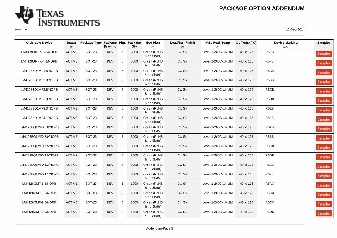
PACKAGE OPTION ADDENDUM
www.ti.com 13-Sep-2014
Addendum-Page 3
Orderable Device Status(1)
Package Type PackageDrawing
Pins PackageQty
Eco Plan(2)
Lead/Ball Finish(6)
MSL Peak Temp(3)
Op Temp (°C) Device Marking(4/5)
Samples
LM4128BMFX-3.3/NOPB ACTIVE SOT-23 DBV 5 3000 Green (RoHS& no Sb/Br)
CU SN Level-1-260C-UNLIM -40 to 125 R5EB
LM4128BMFX-4.1/NOPB ACTIVE SOT-23 DBV 5 3000 Green (RoHS& no Sb/Br)
CU SN Level-1-260C-UNLIM -40 to 125 R5FB
LM4128BQ1MF1.8/NOPB ACTIVE SOT-23 DBV 5 1000 Green (RoHS& no Sb/Br)
CU SN Level-1-260C-UNLIM -40 to 125 R6AB
LM4128BQ1MF2.0/NOPB ACTIVE SOT-23 DBV 5 1000 Green (RoHS& no Sb/Br)
CU SN Level-1-260C-UNLIM -40 to 125 R6BB
LM4128BQ1MF2.5/NOPB ACTIVE SOT-23 DBV 5 1000 Green (RoHS& no Sb/Br)
CU SN Level-1-260C-UNLIM -40 to 125 R6CB
LM4128BQ1MF3.0/NOPB ACTIVE SOT-23 DBV 5 1000 Green (RoHS& no Sb/Br)
CU SN Level-1-260C-UNLIM -40 to 125 R6DB
LM4128BQ1MF3.3/NOPB ACTIVE SOT-23 DBV 5 1000 Green (RoHS& no Sb/Br)
CU SN Level-1-260C-UNLIM -40 to 125 R6EB
LM4128BQ1MF4.1/NOPB ACTIVE SOT-23 DBV 5 1000 Green (RoHS& no Sb/Br)
CU SN Level-1-260C-UNLIM -40 to 125 R6FB
LM4128BQ1MFX1.8/NOPB ACTIVE SOT-23 DBV 5 3000 Green (RoHS& no Sb/Br)
CU SN Level-1-260C-UNLIM -40 to 125 R6AB
LM4128BQ1MFX2.0/NOPB ACTIVE SOT-23 DBV 5 3000 Green (RoHS& no Sb/Br)
CU SN Level-1-260C-UNLIM -40 to 125 R6BB
LM4128BQ1MFX2.5/NOPB ACTIVE SOT-23 DBV 5 3000 Green (RoHS& no Sb/Br)
CU SN Level-1-260C-UNLIM -40 to 125 R6CB
LM4128BQ1MFX3.0/NOPB ACTIVE SOT-23 DBV 5 3000 Green (RoHS& no Sb/Br)
CU SN Level-1-260C-UNLIM -40 to 125 R6DB
LM4128BQ1MFX3.3/NOPB ACTIVE SOT-23 DBV 5 3000 Green (RoHS& no Sb/Br)
CU SN Level-1-260C-UNLIM -40 to 125 R6EB
LM4128BQ1MFX4.1/NOPB ACTIVE SOT-23 DBV 5 3000 Green (RoHS& no Sb/Br)
CU SN Level-1-260C-UNLIM -40 to 125 R6FB
LM4128CMF-1.8/NOPB ACTIVE SOT-23 DBV 5 1000 Green (RoHS& no Sb/Br)
CU SN Level-1-260C-UNLIM -40 to 125 R5AC
LM4128CMF-2.0/NOPB ACTIVE SOT-23 DBV 5 1000 Green (RoHS& no Sb/Br)
CU SN Level-1-260C-UNLIM -40 to 125 R5BC
LM4128CMF-2.5/NOPB ACTIVE SOT-23 DBV 5 1000 Green (RoHS& no Sb/Br)
CU SN Level-1-260C-UNLIM -40 to 125 R5CC
LM4128CMF-3.0/NOPB ACTIVE SOT-23 DBV 5 1000 Green (RoHS& no Sb/Br)
CU SN Level-1-260C-UNLIM -40 to 125 R5DC
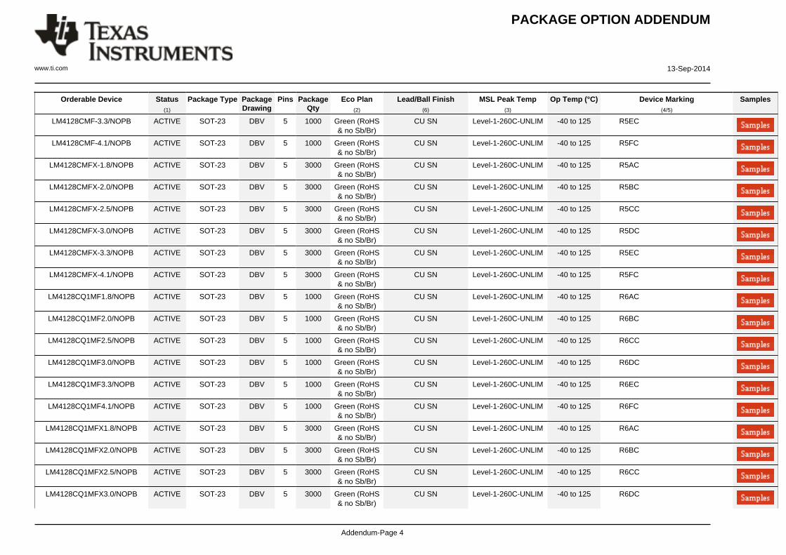
PACKAGE OPTION ADDENDUM
www.ti.com 13-Sep-2014
Addendum-Page 4
Orderable Device Status(1)
Package Type PackageDrawing
Pins PackageQty
Eco Plan(2)
Lead/Ball Finish(6)
MSL Peak Temp(3)
Op Temp (°C) Device Marking(4/5)
Samples
LM4128CMF-3.3/NOPB ACTIVE SOT-23 DBV 5 1000 Green (RoHS& no Sb/Br)
CU SN Level-1-260C-UNLIM -40 to 125 R5EC
LM4128CMF-4.1/NOPB ACTIVE SOT-23 DBV 5 1000 Green (RoHS& no Sb/Br)
CU SN Level-1-260C-UNLIM -40 to 125 R5FC
LM4128CMFX-1.8/NOPB ACTIVE SOT-23 DBV 5 3000 Green (RoHS& no Sb/Br)
CU SN Level-1-260C-UNLIM -40 to 125 R5AC
LM4128CMFX-2.0/NOPB ACTIVE SOT-23 DBV 5 3000 Green (RoHS& no Sb/Br)
CU SN Level-1-260C-UNLIM -40 to 125 R5BC
LM4128CMFX-2.5/NOPB ACTIVE SOT-23 DBV 5 3000 Green (RoHS& no Sb/Br)
CU SN Level-1-260C-UNLIM -40 to 125 R5CC
LM4128CMFX-3.0/NOPB ACTIVE SOT-23 DBV 5 3000 Green (RoHS& no Sb/Br)
CU SN Level-1-260C-UNLIM -40 to 125 R5DC
LM4128CMFX-3.3/NOPB ACTIVE SOT-23 DBV 5 3000 Green (RoHS& no Sb/Br)
CU SN Level-1-260C-UNLIM -40 to 125 R5EC
LM4128CMFX-4.1/NOPB ACTIVE SOT-23 DBV 5 3000 Green (RoHS& no Sb/Br)
CU SN Level-1-260C-UNLIM -40 to 125 R5FC
LM4128CQ1MF1.8/NOPB ACTIVE SOT-23 DBV 5 1000 Green (RoHS& no Sb/Br)
CU SN Level-1-260C-UNLIM -40 to 125 R6AC
LM4128CQ1MF2.0/NOPB ACTIVE SOT-23 DBV 5 1000 Green (RoHS& no Sb/Br)
CU SN Level-1-260C-UNLIM -40 to 125 R6BC
LM4128CQ1MF2.5/NOPB ACTIVE SOT-23 DBV 5 1000 Green (RoHS& no Sb/Br)
CU SN Level-1-260C-UNLIM -40 to 125 R6CC
LM4128CQ1MF3.0/NOPB ACTIVE SOT-23 DBV 5 1000 Green (RoHS& no Sb/Br)
CU SN Level-1-260C-UNLIM -40 to 125 R6DC
LM4128CQ1MF3.3/NOPB ACTIVE SOT-23 DBV 5 1000 Green (RoHS& no Sb/Br)
CU SN Level-1-260C-UNLIM -40 to 125 R6EC
LM4128CQ1MF4.1/NOPB ACTIVE SOT-23 DBV 5 1000 Green (RoHS& no Sb/Br)
CU SN Level-1-260C-UNLIM -40 to 125 R6FC
LM4128CQ1MFX1.8/NOPB ACTIVE SOT-23 DBV 5 3000 Green (RoHS& no Sb/Br)
CU SN Level-1-260C-UNLIM -40 to 125 R6AC
LM4128CQ1MFX2.0/NOPB ACTIVE SOT-23 DBV 5 3000 Green (RoHS& no Sb/Br)
CU SN Level-1-260C-UNLIM -40 to 125 R6BC
LM4128CQ1MFX2.5/NOPB ACTIVE SOT-23 DBV 5 3000 Green (RoHS& no Sb/Br)
CU SN Level-1-260C-UNLIM -40 to 125 R6CC
LM4128CQ1MFX3.0/NOPB ACTIVE SOT-23 DBV 5 3000 Green (RoHS& no Sb/Br)
CU SN Level-1-260C-UNLIM -40 to 125 R6DC

PACKAGE OPTION ADDENDUM
www.ti.com 13-Sep-2014
Addendum-Page 5
Orderable Device Status(1)
Package Type PackageDrawing
Pins PackageQty
Eco Plan(2)
Lead/Ball Finish(6)
MSL Peak Temp(3)
Op Temp (°C) Device Marking(4/5)
Samples
LM4128CQ1MFX3.3/NOPB ACTIVE SOT-23 DBV 5 3000 Green (RoHS& no Sb/Br)
CU SN Level-1-260C-UNLIM -40 to 125 R6EC
LM4128CQ1MFX4.1/NOPB ACTIVE SOT-23 DBV 5 3000 Green (RoHS& no Sb/Br)
CU SN Level-1-260C-UNLIM -40 to 125 R6FC
LM4128DMF-1.8/NOPB ACTIVE SOT-23 DBV 5 1000 Green (RoHS& no Sb/Br)
CU SN Level-1-260C-UNLIM -40 to 125 R5AD
LM4128DMF-2.0/NOPB ACTIVE SOT-23 DBV 5 1000 Green (RoHS& no Sb/Br)
CU SN Level-1-260C-UNLIM -40 to 125 R5BD
LM4128DMF-2.5/NOPB ACTIVE SOT-23 DBV 5 1000 Green (RoHS& no Sb/Br)
CU SN Level-1-260C-UNLIM -40 to 125 R5CD
LM4128DMF-3.0/NOPB ACTIVE SOT-23 DBV 5 1000 Green (RoHS& no Sb/Br)
CU SN Level-1-260C-UNLIM -40 to 125 R5DD
LM4128DMF-3.3/NOPB ACTIVE SOT-23 DBV 5 1000 Green (RoHS& no Sb/Br)
CU SN Level-1-260C-UNLIM -40 to 125 R5ED
LM4128DMF-4.1/NOPB ACTIVE SOT-23 DBV 5 1000 Green (RoHS& no Sb/Br)
CU SN Level-1-260C-UNLIM -40 to 125 R5FD
LM4128DMFX-1.8/NOPB ACTIVE SOT-23 DBV 5 3000 Green (RoHS& no Sb/Br)
CU SN Level-1-260C-UNLIM -40 to 125 R5AD
LM4128DMFX-2.0/NOPB ACTIVE SOT-23 DBV 5 3000 Green (RoHS& no Sb/Br)
CU SN Level-1-260C-UNLIM -40 to 125 R5BD
LM4128DMFX-2.5/NOPB ACTIVE SOT-23 DBV 5 3000 Green (RoHS& no Sb/Br)
CU SN Level-1-260C-UNLIM -40 to 125 R5CD
LM4128DMFX-3.0/NOPB ACTIVE SOT-23 DBV 5 3000 Green (RoHS& no Sb/Br)
CU SN Level-1-260C-UNLIM -40 to 125 R5DD
LM4128DMFX-3.3/NOPB ACTIVE SOT-23 DBV 5 3000 Green (RoHS& no Sb/Br)
CU SN Level-1-260C-UNLIM -40 to 125 R5ED
LM4128DMFX-4.1/NOPB ACTIVE SOT-23 DBV 5 3000 Green (RoHS& no Sb/Br)
CU SN Level-1-260C-UNLIM -40 to 125 R5FD
LM4128DQ1MF1.8/NOPB ACTIVE SOT-23 DBV 5 1000 Green (RoHS& no Sb/Br)
CU SN Level-1-260C-UNLIM -40 to 125 R6AD
LM4128DQ1MF2.0/NOPB ACTIVE SOT-23 DBV 5 1000 Green (RoHS& no Sb/Br)
CU SN Level-1-260C-UNLIM -40 to 125 R6BD
LM4128DQ1MF2.5/NOPB ACTIVE SOT-23 DBV 5 1000 Green (RoHS& no Sb/Br)
CU SN Level-1-260C-UNLIM -40 to 125 R6CD
LM4128DQ1MF3.0/NOPB ACTIVE SOT-23 DBV 5 1000 Green (RoHS& no Sb/Br)
CU SN Level-1-260C-UNLIM -40 to 125 R6DD
PACKAGE OPTION ADDENDUM
www.ti.com 13-Sep-2014
Addendum-Page 6
Orderable Device Status(1)
Package Type PackageDrawing
Pins PackageQty
Eco Plan(2)
Lead/Ball Finish(6)
MSL Peak Temp(3)
Op Temp (°C) Device Marking(4/5)
Samples
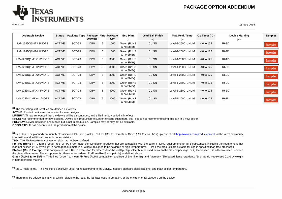
LM4128DQ1MF3.3/NOPB ACTIVE SOT-23 DBV 5 1000 Green (RoHS& no Sb/Br)
CU SN Level-1-260C-UNLIM -40 to 125 R6ED
LM4128DQ1MF4.1/NOPB ACTIVE SOT-23 DBV 5 1000 Green (RoHS& no Sb/Br)
CU SN Level-1-260C-UNLIM -40 to 125 R6FD
LM4128DQ1MFX1.8/NOPB ACTIVE SOT-23 DBV 5 3000 Green (RoHS& no Sb/Br)
CU SN Level-1-260C-UNLIM -40 to 125 R6AD
LM4128DQ1MFX2.0/NOPB ACTIVE SOT-23 DBV 5 3000 Green (RoHS& no Sb/Br)
CU SN Level-1-260C-UNLIM -40 to 125 R6BD
LM4128DQ1MFX2.5/NOPB ACTIVE SOT-23 DBV 5 3000 Green (RoHS& no Sb/Br)
CU SN Level-1-260C-UNLIM -40 to 125 R6CD
LM4128DQ1MFX3.0/NOPB ACTIVE SOT-23 DBV 5 3000 Green (RoHS& no Sb/Br)
CU SN Level-1-260C-UNLIM -40 to 125 R6DD
LM4128DQ1MFX3.3/NOPB ACTIVE SOT-23 DBV 5 3000 Green (RoHS& no Sb/Br)
CU SN Level-1-260C-UNLIM -40 to 125 R6ED
LM4128DQ1MFX4.1/NOPB ACTIVE SOT-23 DBV 5 3000 Green (RoHS& no Sb/Br)
CU SN Level-1-260C-UNLIM -40 to 125 R6FD
(1) The marketing status values are defined as follows:ACTIVE: Product device recommended for new designs.LIFEBUY: TI has announced that the device will be discontinued, and a lifetime-buy period is in effect.NRND: Not recommended for new designs. Device is in production to support existing customers, but TI does not recommend using this part in a new design.PREVIEW: Device has been announced but is not in production. Samples may or may not be available.OBSOLETE: TI has discontinued the production of the device.
(2) Eco Plan - The planned eco-friendly classification: Pb-Free (RoHS), Pb-Free (RoHS Exempt), or Green (RoHS & no Sb/Br) - please check http://www.ti.com/productcontent for the latest availabilityinformation and additional product content details.TBD: The Pb-Free/Green conversion plan has not been defined.Pb-Free (RoHS): TI's terms "Lead-Free" or "Pb-Free" mean semiconductor products that are compatible with the current RoHS requirements for all 6 substances, including the requirement thatlead not exceed 0.1% by weight in homogeneous materials. Where designed to be soldered at high temperatures, TI Pb-Free products are suitable for use in specified lead-free processes.Pb-Free (RoHS Exempt): This component has a RoHS exemption for either 1) lead-based flip-chip solder bumps used between the die and package, or 2) lead-based die adhesive used betweenthe die and leadframe. The component is otherwise considered Pb-Free (RoHS compatible) as defined above.Green (RoHS & no Sb/Br): TI defines "Green" to mean Pb-Free (RoHS compatible), and free of Bromine (Br) and Antimony (Sb) based flame retardants (Br or Sb do not exceed 0.1% by weightin homogeneous material)
(3) MSL, Peak Temp. - The Moisture Sensitivity Level rating according to the JEDEC industry standard classifications, and peak solder temperature.
(4) There may be additional marking, which relates to the logo, the lot trace code information, or the environmental category on the device.
PACKAGE OPTION ADDENDUM
www.ti.com 13-Sep-2014
Addendum-Page 7
(5) Multiple Device Markings will be inside parentheses. Only one Device Marking contained in parentheses and separated by a "~" will appear on a device. If a line is indented then it is a continuationof the previous line and the two combined represent the entire Device Marking for that device.
(6) Lead/Ball Finish - Orderable Devices may have multiple material finish options. Finish options are separated by a vertical ruled line. Lead/Ball Finish values may wrap to two lines if the finishvalue exceeds the maximum column width.
Important Information and Disclaimer:The information provided on this page represents TI's knowledge and belief as of the date that it is provided. TI bases its knowledge and belief on informationprovided by third parties, and makes no representation or warranty as to the accuracy of such information. Efforts are underway to better integrate information from third parties. TI has taken andcontinues to take reasonable steps to provide representative and accurate information but may not have conducted destructive testing or chemical analysis on incoming materials and chemicals.TI and TI suppliers consider certain information to be proprietary, and thus CAS numbers and other limited information may not be available for release.
In no event shall TI's liability arising out of such information exceed the total purchase price of the TI part(s) at issue in this document sold by TI to Customer on an annual basis.
OTHER QUALIFIED VERSIONS OF LM4128, LM4128-Q1 :
• Catalog: LM4128
• Automotive: LM4128-Q1
NOTE: Qualified Version Definitions:
• Catalog - TI's standard catalog product
• Automotive - Q100 devices qualified for high-reliability automotive applications targeting zero defects
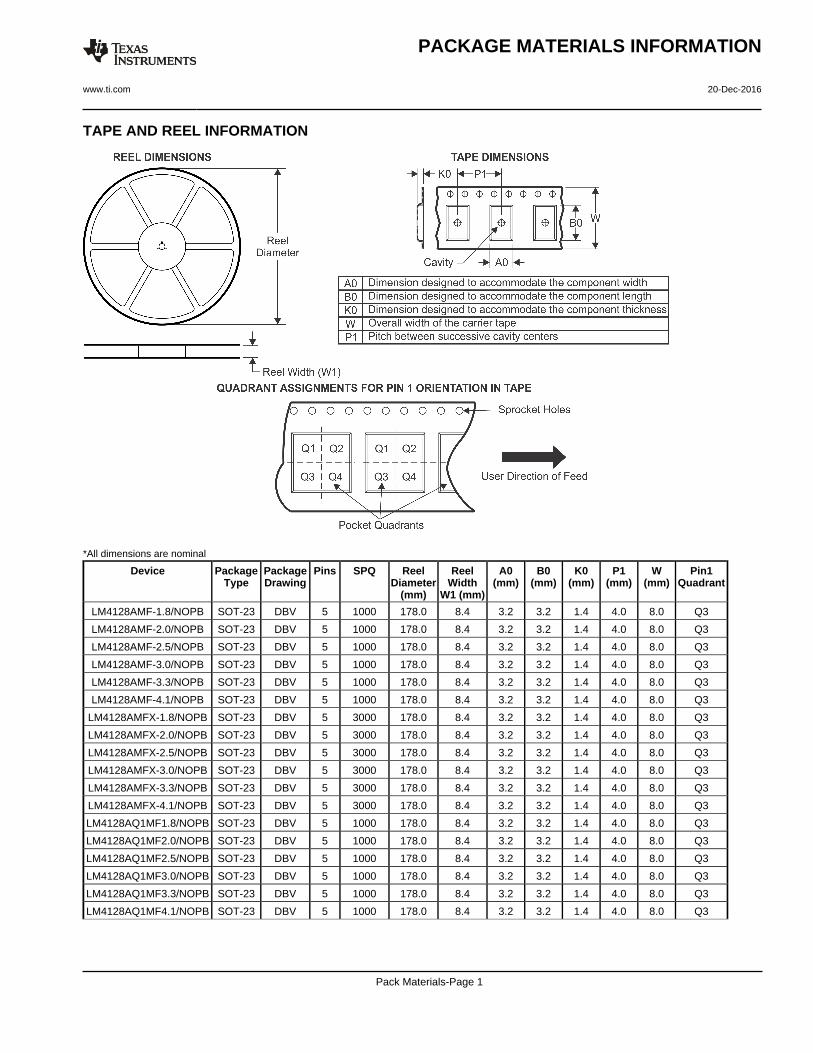
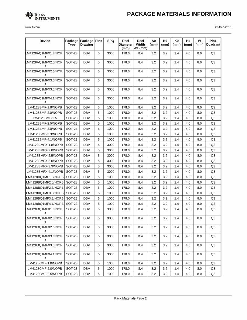
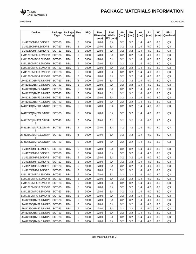
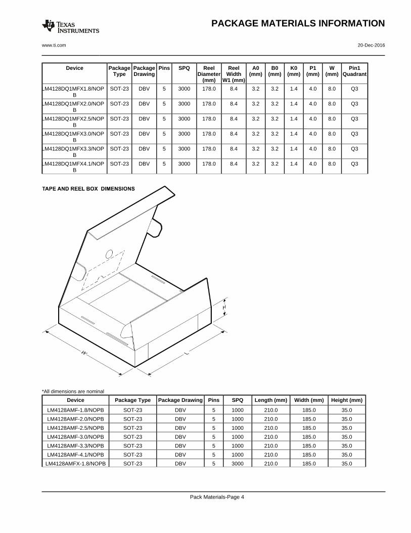
TAPE AND REEL INFORMATION
*All dimensions are nominal
Device PackageType
PackageDrawing
Pins SPQ ReelDiameter
(mm)
ReelWidth
W1 (mm)
A0(mm)
B0(mm)
K0(mm)
P1(mm)
W(mm)
Pin1Quadrant
LM4128AMF-1.8/NOPB SOT-23 DBV 5 1000 178.0 8.4 3.2 3.2 1.4 4.0 8.0 Q3
LM4128AMF-2.0/NOPB SOT-23 DBV 5 1000 178.0 8.4 3.2 3.2 1.4 4.0 8.0 Q3
LM4128AMF-2.5/NOPB SOT-23 DBV 5 1000 178.0 8.4 3.2 3.2 1.4 4.0 8.0 Q3
LM4128AMF-3.0/NOPB SOT-23 DBV 5 1000 178.0 8.4 3.2 3.2 1.4 4.0 8.0 Q3
LM4128AMF-3.3/NOPB SOT-23 DBV 5 1000 178.0 8.4 3.2 3.2 1.4 4.0 8.0 Q3
LM4128AMF-4.1/NOPB SOT-23 DBV 5 1000 178.0 8.4 3.2 3.2 1.4 4.0 8.0 Q3
LM4128AMFX-1.8/NOPB SOT-23 DBV 5 3000 178.0 8.4 3.2 3.2 1.4 4.0 8.0 Q3
LM4128AMFX-2.0/NOPB SOT-23 DBV 5 3000 178.0 8.4 3.2 3.2 1.4 4.0 8.0 Q3
LM4128AMFX-2.5/NOPB SOT-23 DBV 5 3000 178.0 8.4 3.2 3.2 1.4 4.0 8.0 Q3
LM4128AMFX-3.0/NOPB SOT-23 DBV 5 3000 178.0 8.4 3.2 3.2 1.4 4.0 8.0 Q3
LM4128AMFX-3.3/NOPB SOT-23 DBV 5 3000 178.0 8.4 3.2 3.2 1.4 4.0 8.0 Q3
LM4128AMFX-4.1/NOPB SOT-23 DBV 5 3000 178.0 8.4 3.2 3.2 1.4 4.0 8.0 Q3
LM4128AQ1MF1.8/NOPB SOT-23 DBV 5 1000 178.0 8.4 3.2 3.2 1.4 4.0 8.0 Q3
LM4128AQ1MF2.0/NOPB SOT-23 DBV 5 1000 178.0 8.4 3.2 3.2 1.4 4.0 8.0 Q3
LM4128AQ1MF2.5/NOPB SOT-23 DBV 5 1000 178.0 8.4 3.2 3.2 1.4 4.0 8.0 Q3
LM4128AQ1MF3.0/NOPB SOT-23 DBV 5 1000 178.0 8.4 3.2 3.2 1.4 4.0 8.0 Q3
LM4128AQ1MF3.3/NOPB SOT-23 DBV 5 1000 178.0 8.4 3.2 3.2 1.4 4.0 8.0 Q3
LM4128AQ1MF4.1/NOPB SOT-23 DBV 5 1000 178.0 8.4 3.2 3.2 1.4 4.0 8.0 Q3
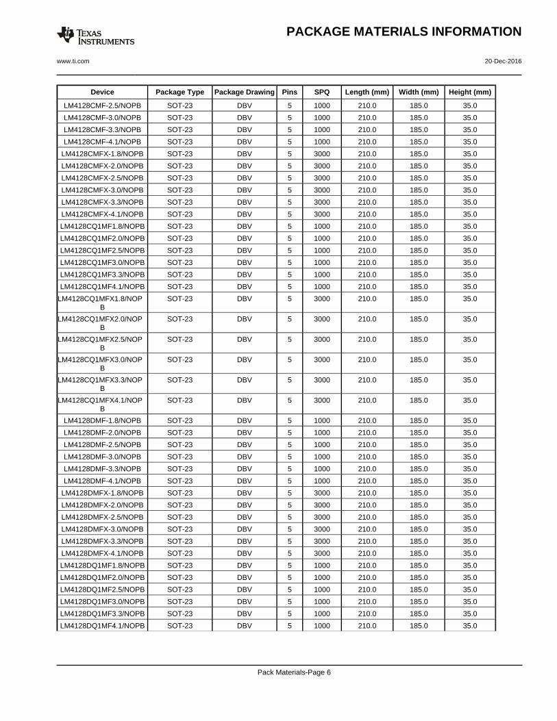
PACKAGE MATERIALS INFORMATION
www.ti.com 20-Dec-2016
Pack Materials-Page 1
Device PackageType
PackageDrawing
Pins SPQ ReelDiameter
(mm)
ReelWidth
W1 (mm)
A0(mm)
B0(mm)
K0(mm)
P1(mm)
W(mm)
Pin1Quadrant
LM4128AQ1MFX1.8/NOPB
SOT-23 DBV 5 3000 178.0 8.4 3.2 3.2 1.4 4.0 8.0 Q3
LM4128AQ1MFX2.0/NOPB
SOT-23 DBV 5 3000 178.0 8.4 3.2 3.2 1.4 4.0 8.0 Q3
LM4128AQ1MFX2.5/NOPB
SOT-23 DBV 5 3000 178.0 8.4 3.2 3.2 1.4 4.0 8.0 Q3
LM4128AQ1MFX3.0/NOPB
SOT-23 DBV 5 3000 178.0 8.4 3.2 3.2 1.4 4.0 8.0 Q3
LM4128AQ1MFX3.3/NOPB
SOT-23 DBV 5 3000 178.0 8.4 3.2 3.2 1.4 4.0 8.0 Q3
LM4128AQ1MFX4.1/NOPB
SOT-23 DBV 5 3000 178.0 8.4 3.2 3.2 1.4 4.0 8.0 Q3
LM4128BMF-1.8/NOPB SOT-23 DBV 5 1000 178.0 8.4 3.2 3.2 1.4 4.0 8.0 Q3
LM4128BMF-2.0/NOPB SOT-23 DBV 5 1000 178.0 8.4 3.2 3.2 1.4 4.0 8.0 Q3
LM4128BMF-2.5 SOT-23 DBV 5 1000 178.0 8.4 3.2 3.2 1.4 4.0 8.0 Q3
LM4128BMF-2.5/NOPB SOT-23 DBV 5 1000 178.0 8.4 3.2 3.2 1.4 4.0 8.0 Q3
LM4128BMF-3.0/NOPB SOT-23 DBV 5 1000 178.0 8.4 3.2 3.2 1.4 4.0 8.0 Q3
LM4128BMF-3.3/NOPB SOT-23 DBV 5 1000 178.0 8.4 3.2 3.2 1.4 4.0 8.0 Q3
LM4128BMF-4.1/NOPB SOT-23 DBV 5 1000 178.0 8.4 3.2 3.2 1.4 4.0 8.0 Q3
LM4128BMFX-1.8/NOPB SOT-23 DBV 5 3000 178.0 8.4 3.2 3.2 1.4 4.0 8.0 Q3
LM4128BMFX-2.0/NOPB SOT-23 DBV 5 3000 178.0 8.4 3.2 3.2 1.4 4.0 8.0 Q3
LM4128BMFX-2.5/NOPB SOT-23 DBV 5 3000 178.0 8.4 3.2 3.2 1.4 4.0 8.0 Q3
LM4128BMFX-3.0/NOPB SOT-23 DBV 5 3000 178.0 8.4 3.2 3.2 1.4 4.0 8.0 Q3
LM4128BMFX-3.3/NOPB SOT-23 DBV 5 3000 178.0 8.4 3.2 3.2 1.4 4.0 8.0 Q3
LM4128BMFX-4.1/NOPB SOT-23 DBV 5 3000 178.0 8.4 3.2 3.2 1.4 4.0 8.0 Q3
LM4128BQ1MF1.8/NOPB SOT-23 DBV 5 1000 178.0 8.4 3.2 3.2 1.4 4.0 8.0 Q3
LM4128BQ1MF2.0/NOPB SOT-23 DBV 5 1000 178.0 8.4 3.2 3.2 1.4 4.0 8.0 Q3
LM4128BQ1MF2.5/NOPB SOT-23 DBV 5 1000 178.0 8.4 3.2 3.2 1.4 4.0 8.0 Q3
LM4128BQ1MF3.0/NOPB SOT-23 DBV 5 1000 178.0 8.4 3.2 3.2 1.4 4.0 8.0 Q3
LM4128BQ1MF3.3/NOPB SOT-23 DBV 5 1000 178.0 8.4 3.2 3.2 1.4 4.0 8.0 Q3
LM4128BQ1MF4.1/NOPB SOT-23 DBV 5 1000 178.0 8.4 3.2 3.2 1.4 4.0 8.0 Q3
LM4128BQ1MFX1.8/NOPB
SOT-23 DBV 5 3000 178.0 8.4 3.2 3.2 1.4 4.0 8.0 Q3
LM4128BQ1MFX2.0/NOPB
SOT-23 DBV 5 3000 178.0 8.4 3.2 3.2 1.4 4.0 8.0 Q3
LM4128BQ1MFX2.5/NOPB
SOT-23 DBV 5 3000 178.0 8.4 3.2 3.2 1.4 4.0 8.0 Q3
LM4128BQ1MFX3.0/NOPB
SOT-23 DBV 5 3000 178.0 8.4 3.2 3.2 1.4 4.0 8.0 Q3
LM4128BQ1MFX3.3/NOPB
SOT-23 DBV 5 3000 178.0 8.4 3.2 3.2 1.4 4.0 8.0 Q3
LM4128BQ1MFX4.1/NOPB
SOT-23 DBV 5 3000 178.0 8.4 3.2 3.2 1.4 4.0 8.0 Q3
LM4128CMF-1.8/NOPB SOT-23 DBV 5 1000 178.0 8.4 3.2 3.2 1.4 4.0 8.0 Q3
LM4128CMF-2.0/NOPB SOT-23 DBV 5 1000 178.0 8.4 3.2 3.2 1.4 4.0 8.0 Q3
LM4128CMF-2.5/NOPB SOT-23 DBV 5 1000 178.0 8.4 3.2 3.2 1.4 4.0 8.0 Q3
PACKAGE MATERIALS INFORMATION
www.ti.com 20-Dec-2016
Pack Materials-Page 2
Device PackageType
PackageDrawing
Pins SPQ ReelDiameter
(mm)
ReelWidth
W1 (mm)
A0(mm)
B0(mm)
K0(mm)
P1(mm)
W(mm)
Pin1Quadrant
LM4128CMF-3.0/NOPB SOT-23 DBV 5 1000 178.0 8.4 3.2 3.2 1.4 4.0 8.0 Q3
LM4128CMF-3.3/NOPB SOT-23 DBV 5 1000 178.0 8.4 3.2 3.2 1.4 4.0 8.0 Q3
LM4128CMF-4.1/NOPB SOT-23 DBV 5 1000 178.0 8.4 3.2 3.2 1.4 4.0 8.0 Q3
LM4128CMFX-1.8/NOPB SOT-23 DBV 5 3000 178.0 8.4 3.2 3.2 1.4 4.0 8.0 Q3
LM4128CMFX-2.0/NOPB SOT-23 DBV 5 3000 178.0 8.4 3.2 3.2 1.4 4.0 8.0 Q3
LM4128CMFX-2.5/NOPB SOT-23 DBV 5 3000 178.0 8.4 3.2 3.2 1.4 4.0 8.0 Q3
LM4128CMFX-3.0/NOPB SOT-23 DBV 5 3000 178.0 8.4 3.2 3.2 1.4 4.0 8.0 Q3
LM4128CMFX-3.3/NOPB SOT-23 DBV 5 3000 178.0 8.4 3.2 3.2 1.4 4.0 8.0 Q3
LM4128CMFX-4.1/NOPB SOT-23 DBV 5 3000 178.0 8.4 3.2 3.2 1.4 4.0 8.0 Q3
LM4128CQ1MF1.8/NOPB SOT-23 DBV 5 1000 178.0 8.4 3.2 3.2 1.4 4.0 8.0 Q3
LM4128CQ1MF2.0/NOPB SOT-23 DBV 5 1000 178.0 8.4 3.2 3.2 1.4 4.0 8.0 Q3
LM4128CQ1MF2.5/NOPB SOT-23 DBV 5 1000 178.0 8.4 3.2 3.2 1.4 4.0 8.0 Q3
LM4128CQ1MF3.0/NOPB SOT-23 DBV 5 1000 178.0 8.4 3.2 3.2 1.4 4.0 8.0 Q3
LM4128CQ1MF3.3/NOPB SOT-23 DBV 5 1000 178.0 8.4 3.2 3.2 1.4 4.0 8.0 Q3
LM4128CQ1MF4.1/NOPB SOT-23 DBV 5 1000 178.0 8.4 3.2 3.2 1.4 4.0 8.0 Q3
LM4128CQ1MFX1.8/NOPB
SOT-23 DBV 5 3000 178.0 8.4 3.2 3.2 1.4 4.0 8.0 Q3
LM4128CQ1MFX2.0/NOPB
SOT-23 DBV 5 3000 178.0 8.4 3.2 3.2 1.4 4.0 8.0 Q3
LM4128CQ1MFX2.5/NOPB
SOT-23 DBV 5 3000 178.0 8.4 3.2 3.2 1.4 4.0 8.0 Q3
LM4128CQ1MFX3.0/NOPB
SOT-23 DBV 5 3000 178.0 8.4 3.2 3.2 1.4 4.0 8.0 Q3
LM4128CQ1MFX3.3/NOPB
SOT-23 DBV 5 3000 178.0 8.4 3.2 3.2 1.4 4.0 8.0 Q3
LM4128CQ1MFX4.1/NOPB
SOT-23 DBV 5 3000 178.0 8.4 3.2 3.2 1.4 4.0 8.0 Q3
LM4128DMF-1.8/NOPB SOT-23 DBV 5 1000 178.0 8.4 3.2 3.2 1.4 4.0 8.0 Q3
LM4128DMF-2.0/NOPB SOT-23 DBV 5 1000 178.0 8.4 3.2 3.2 1.4 4.0 8.0 Q3
LM4128DMF-2.5/NOPB SOT-23 DBV 5 1000 178.0 8.4 3.2 3.2 1.4 4.0 8.0 Q3
LM4128DMF-3.0/NOPB SOT-23 DBV 5 1000 178.0 8.4 3.2 3.2 1.4 4.0 8.0 Q3
LM4128DMF-3.3/NOPB SOT-23 DBV 5 1000 178.0 8.4 3.2 3.2 1.4 4.0 8.0 Q3
LM4128DMF-4.1/NOPB SOT-23 DBV 5 1000 178.0 8.4 3.2 3.2 1.4 4.0 8.0 Q3
LM4128DMFX-1.8/NOPB SOT-23 DBV 5 3000 178.0 8.4 3.2 3.2 1.4 4.0 8.0 Q3
LM4128DMFX-2.0/NOPB SOT-23 DBV 5 3000 178.0 8.4 3.2 3.2 1.4 4.0 8.0 Q3
LM4128DMFX-2.5/NOPB SOT-23 DBV 5 3000 178.0 8.4 3.2 3.2 1.4 4.0 8.0 Q3
LM4128DMFX-3.0/NOPB SOT-23 DBV 5 3000 178.0 8.4 3.2 3.2 1.4 4.0 8.0 Q3
LM4128DMFX-3.3/NOPB SOT-23 DBV 5 3000 178.0 8.4 3.2 3.2 1.4 4.0 8.0 Q3
LM4128DMFX-4.1/NOPB SOT-23 DBV 5 3000 178.0 8.4 3.2 3.2 1.4 4.0 8.0 Q3
LM4128DQ1MF1.8/NOPB SOT-23 DBV 5 1000 178.0 8.4 3.2 3.2 1.4 4.0 8.0 Q3
LM4128DQ1MF2.0/NOPB SOT-23 DBV 5 1000 178.0 8.4 3.2 3.2 1.4 4.0 8.0 Q3
LM4128DQ1MF2.5/NOPB SOT-23 DBV 5 1000 178.0 8.4 3.2 3.2 1.4 4.0 8.0 Q3
LM4128DQ1MF3.0/NOPB SOT-23 DBV 5 1000 178.0 8.4 3.2 3.2 1.4 4.0 8.0 Q3
LM4128DQ1MF3.3/NOPB SOT-23 DBV 5 1000 178.0 8.4 3.2 3.2 1.4 4.0 8.0 Q3
LM4128DQ1MF4.1/NOPB SOT-23 DBV 5 1000 178.0 8.4 3.2 3.2 1.4 4.0 8.0 Q3
PACKAGE MATERIALS INFORMATION
www.ti.com 20-Dec-2016
Pack Materials-Page 3
Device PackageType
PackageDrawing
Pins SPQ ReelDiameter
(mm)
ReelWidth
W1 (mm)
A0(mm)
B0(mm)
K0(mm)
P1(mm)
W(mm)
Pin1Quadrant
LM4128DQ1MFX1.8/NOPB
SOT-23 DBV 5 3000 178.0 8.4 3.2 3.2 1.4 4.0 8.0 Q3
LM4128DQ1MFX2.0/NOPB
SOT-23 DBV 5 3000 178.0 8.4 3.2 3.2 1.4 4.0 8.0 Q3
LM4128DQ1MFX2.5/NOPB
SOT-23 DBV 5 3000 178.0 8.4 3.2 3.2 1.4 4.0 8.0 Q3
LM4128DQ1MFX3.0/NOPB
SOT-23 DBV 5 3000 178.0 8.4 3.2 3.2 1.4 4.0 8.0 Q3
LM4128DQ1MFX3.3/NOPB
SOT-23 DBV 5 3000 178.0 8.4 3.2 3.2 1.4 4.0 8.0 Q3
LM4128DQ1MFX4.1/NOPB
SOT-23 DBV 5 3000 178.0 8.4 3.2 3.2 1.4 4.0 8.0 Q3
*All dimensions are nominal
Device Package Type Package Drawing Pins SPQ Length (mm) Width (mm) Height (mm)
LM4128AMF-1.8/NOPB SOT-23 DBV 5 1000 210.0 185.0 35.0
LM4128AMF-2.0/NOPB SOT-23 DBV 5 1000 210.0 185.0 35.0
LM4128AMF-2.5/NOPB SOT-23 DBV 5 1000 210.0 185.0 35.0
LM4128AMF-3.0/NOPB SOT-23 DBV 5 1000 210.0 185.0 35.0
LM4128AMF-3.3/NOPB SOT-23 DBV 5 1000 210.0 185.0 35.0
LM4128AMF-4.1/NOPB SOT-23 DBV 5 1000 210.0 185.0 35.0
LM4128AMFX-1.8/NOPB SOT-23 DBV 5 3000 210.0 185.0 35.0
PACKAGE MATERIALS INFORMATION
www.ti.com 20-Dec-2016
Pack Materials-Page 4
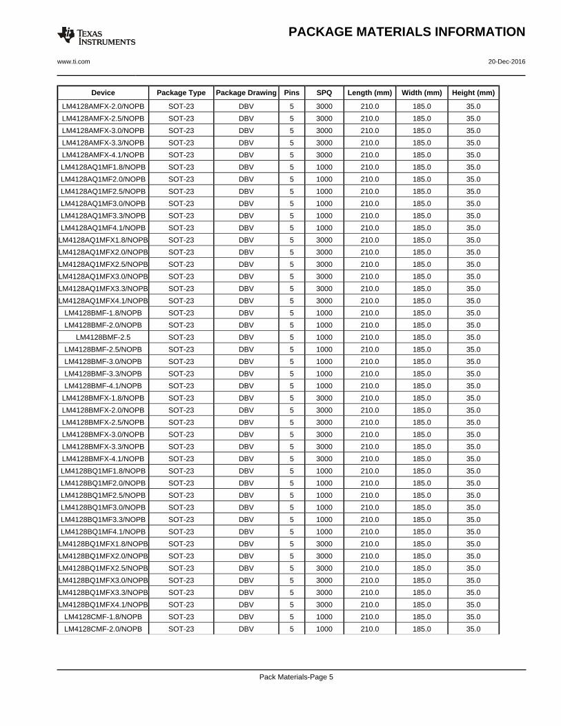
Device Package Type Package Drawing Pins SPQ Length (mm) Width (mm) Height (mm)
LM4128AMFX-2.0/NOPB SOT-23 DBV 5 3000 210.0 185.0 35.0
LM4128AMFX-2.5/NOPB SOT-23 DBV 5 3000 210.0 185.0 35.0
LM4128AMFX-3.0/NOPB SOT-23 DBV 5 3000 210.0 185.0 35.0
LM4128AMFX-3.3/NOPB SOT-23 DBV 5 3000 210.0 185.0 35.0
LM4128AMFX-4.1/NOPB SOT-23 DBV 5 3000 210.0 185.0 35.0
LM4128AQ1MF1.8/NOPB SOT-23 DBV 5 1000 210.0 185.0 35.0
LM4128AQ1MF2.0/NOPB SOT-23 DBV 5 1000 210.0 185.0 35.0
LM4128AQ1MF2.5/NOPB SOT-23 DBV 5 1000 210.0 185.0 35.0
LM4128AQ1MF3.0/NOPB SOT-23 DBV 5 1000 210.0 185.0 35.0
LM4128AQ1MF3.3/NOPB SOT-23 DBV 5 1000 210.0 185.0 35.0
LM4128AQ1MF4.1/NOPB SOT-23 DBV 5 1000 210.0 185.0 35.0
LM4128AQ1MFX1.8/NOPB SOT-23 DBV 5 3000 210.0 185.0 35.0
LM4128AQ1MFX2.0/NOPB SOT-23 DBV 5 3000 210.0 185.0 35.0
LM4128AQ1MFX2.5/NOPB SOT-23 DBV 5 3000 210.0 185.0 35.0
LM4128AQ1MFX3.0/NOPB SOT-23 DBV 5 3000 210.0 185.0 35.0
LM4128AQ1MFX3.3/NOPB SOT-23 DBV 5 3000 210.0 185.0 35.0
LM4128AQ1MFX4.1/NOPB SOT-23 DBV 5 3000 210.0 185.0 35.0
LM4128BMF-1.8/NOPB SOT-23 DBV 5 1000 210.0 185.0 35.0
LM4128BMF-2.0/NOPB SOT-23 DBV 5 1000 210.0 185.0 35.0
LM4128BMF-2.5 SOT-23 DBV 5 1000 210.0 185.0 35.0
LM4128BMF-2.5/NOPB SOT-23 DBV 5 1000 210.0 185.0 35.0
LM4128BMF-3.0/NOPB SOT-23 DBV 5 1000 210.0 185.0 35.0
LM4128BMF-3.3/NOPB SOT-23 DBV 5 1000 210.0 185.0 35.0
LM4128BMF-4.1/NOPB SOT-23 DBV 5 1000 210.0 185.0 35.0
LM4128BMFX-1.8/NOPB SOT-23 DBV 5 3000 210.0 185.0 35.0
LM4128BMFX-2.0/NOPB SOT-23 DBV 5 3000 210.0 185.0 35.0
LM4128BMFX-2.5/NOPB SOT-23 DBV 5 3000 210.0 185.0 35.0
LM4128BMFX-3.0/NOPB SOT-23 DBV 5 3000 210.0 185.0 35.0
LM4128BMFX-3.3/NOPB SOT-23 DBV 5 3000 210.0 185.0 35.0
LM4128BMFX-4.1/NOPB SOT-23 DBV 5 3000 210.0 185.0 35.0
LM4128BQ1MF1.8/NOPB SOT-23 DBV 5 1000 210.0 185.0 35.0
LM4128BQ1MF2.0/NOPB SOT-23 DBV 5 1000 210.0 185.0 35.0
LM4128BQ1MF2.5/NOPB SOT-23 DBV 5 1000 210.0 185.0 35.0
LM4128BQ1MF3.0/NOPB SOT-23 DBV 5 1000 210.0 185.0 35.0
LM4128BQ1MF3.3/NOPB SOT-23 DBV 5 1000 210.0 185.0 35.0
LM4128BQ1MF4.1/NOPB SOT-23 DBV 5 1000 210.0 185.0 35.0
LM4128BQ1MFX1.8/NOPB SOT-23 DBV 5 3000 210.0 185.0 35.0
LM4128BQ1MFX2.0/NOPB SOT-23 DBV 5 3000 210.0 185.0 35.0
LM4128BQ1MFX2.5/NOPB SOT-23 DBV 5 3000 210.0 185.0 35.0
LM4128BQ1MFX3.0/NOPB SOT-23 DBV 5 3000 210.0 185.0 35.0
LM4128BQ1MFX3.3/NOPB SOT-23 DBV 5 3000 210.0 185.0 35.0
LM4128BQ1MFX4.1/NOPB SOT-23 DBV 5 3000 210.0 185.0 35.0
LM4128CMF-1.8/NOPB SOT-23 DBV 5 1000 210.0 185.0 35.0
LM4128CMF-2.0/NOPB SOT-23 DBV 5 1000 210.0 185.0 35.0
PACKAGE MATERIALS INFORMATION
www.ti.com 20-Dec-2016
Pack Materials-Page 5
Device Package Type Package Drawing Pins SPQ Length (mm) Width (mm) Height (mm)
LM4128CMF-2.5/NOPB SOT-23 DBV 5 1000 210.0 185.0 35.0
LM4128CMF-3.0/NOPB SOT-23 DBV 5 1000 210.0 185.0 35.0
LM4128CMF-3.3/NOPB SOT-23 DBV 5 1000 210.0 185.0 35.0
LM4128CMF-4.1/NOPB SOT-23 DBV 5 1000 210.0 185.0 35.0
LM4128CMFX-1.8/NOPB SOT-23 DBV 5 3000 210.0 185.0 35.0
LM4128CMFX-2.0/NOPB SOT-23 DBV 5 3000 210.0 185.0 35.0
LM4128CMFX-2.5/NOPB SOT-23 DBV 5 3000 210.0 185.0 35.0
LM4128CMFX-3.0/NOPB SOT-23 DBV 5 3000 210.0 185.0 35.0
LM4128CMFX-3.3/NOPB SOT-23 DBV 5 3000 210.0 185.0 35.0
LM4128CMFX-4.1/NOPB SOT-23 DBV 5 3000 210.0 185.0 35.0
LM4128CQ1MF1.8/NOPB SOT-23 DBV 5 1000 210.0 185.0 35.0
LM4128CQ1MF2.0/NOPB SOT-23 DBV 5 1000 210.0 185.0 35.0
LM4128CQ1MF2.5/NOPB SOT-23 DBV 5 1000 210.0 185.0 35.0
LM4128CQ1MF3.0/NOPB SOT-23 DBV 5 1000 210.0 185.0 35.0
LM4128CQ1MF3.3/NOPB SOT-23 DBV 5 1000 210.0 185.0 35.0
LM4128CQ1MF4.1/NOPB SOT-23 DBV 5 1000 210.0 185.0 35.0
LM4128CQ1MFX1.8/NOPB
SOT-23 DBV 5 3000 210.0 185.0 35.0
LM4128CQ1MFX2.0/NOPB
SOT-23 DBV 5 3000 210.0 185.0 35.0
LM4128CQ1MFX2.5/NOPB
SOT-23 DBV 5 3000 210.0 185.0 35.0
LM4128CQ1MFX3.0/NOPB
SOT-23 DBV 5 3000 210.0 185.0 35.0
LM4128CQ1MFX3.3/NOPB
SOT-23 DBV 5 3000 210.0 185.0 35.0
LM4128CQ1MFX4.1/NOPB
SOT-23 DBV 5 3000 210.0 185.0 35.0
LM4128DMF-1.8/NOPB SOT-23 DBV 5 1000 210.0 185.0 35.0
LM4128DMF-2.0/NOPB SOT-23 DBV 5 1000 210.0 185.0 35.0
LM4128DMF-2.5/NOPB SOT-23 DBV 5 1000 210.0 185.0 35.0
LM4128DMF-3.0/NOPB SOT-23 DBV 5 1000 210.0 185.0 35.0
LM4128DMF-3.3/NOPB SOT-23 DBV 5 1000 210.0 185.0 35.0
LM4128DMF-4.1/NOPB SOT-23 DBV 5 1000 210.0 185.0 35.0
LM4128DMFX-1.8/NOPB SOT-23 DBV 5 3000 210.0 185.0 35.0
LM4128DMFX-2.0/NOPB SOT-23 DBV 5 3000 210.0 185.0 35.0
LM4128DMFX-2.5/NOPB SOT-23 DBV 5 3000 210.0 185.0 35.0
LM4128DMFX-3.0/NOPB SOT-23 DBV 5 3000 210.0 185.0 35.0
LM4128DMFX-3.3/NOPB SOT-23 DBV 5 3000 210.0 185.0 35.0
LM4128DMFX-4.1/NOPB SOT-23 DBV 5 3000 210.0 185.0 35.0
LM4128DQ1MF1.8/NOPB SOT-23 DBV 5 1000 210.0 185.0 35.0
LM4128DQ1MF2.0/NOPB SOT-23 DBV 5 1000 210.0 185.0 35.0
LM4128DQ1MF2.5/NOPB SOT-23 DBV 5 1000 210.0 185.0 35.0
LM4128DQ1MF3.0/NOPB SOT-23 DBV 5 1000 210.0 185.0 35.0
LM4128DQ1MF3.3/NOPB SOT-23 DBV 5 1000 210.0 185.0 35.0
LM4128DQ1MF4.1/NOPB SOT-23 DBV 5 1000 210.0 185.0 35.0
PACKAGE MATERIALS INFORMATION
www.ti.com 20-Dec-2016
Pack Materials-Page 6
Device Package Type Package Drawing Pins SPQ Length (mm) Width (mm) Height (mm)
LM4128DQ1MFX1.8/NOPB
SOT-23 DBV 5 3000 210.0 185.0 35.0
LM4128DQ1MFX2.0/NOPB
SOT-23 DBV 5 3000 210.0 185.0 35.0
LM4128DQ1MFX2.5/NOPB
SOT-23 DBV 5 3000 210.0 185.0 35.0
LM4128DQ1MFX3.0/NOPB
SOT-23 DBV 5 3000 210.0 185.0 35.0
LM4128DQ1MFX3.3/NOPB
SOT-23 DBV 5 3000 210.0 185.0 35.0
LM4128DQ1MFX4.1/NOPB
SOT-23 DBV 5 3000 210.0 185.0 35.0
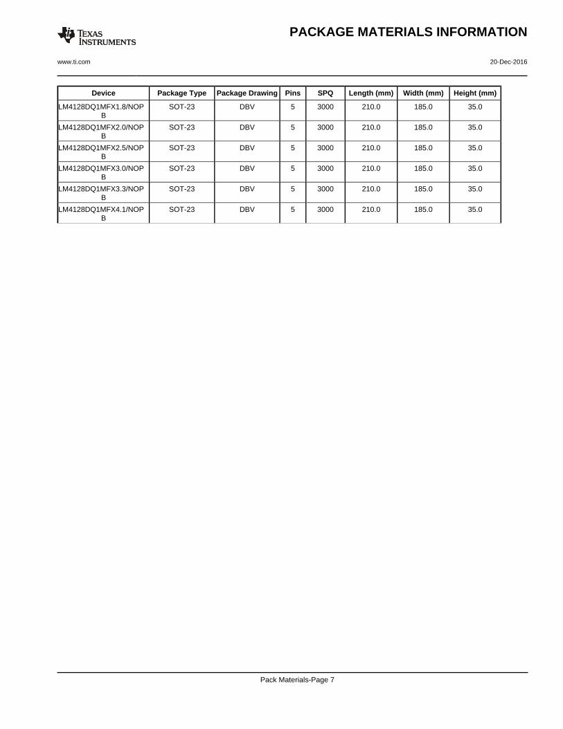
PACKAGE MATERIALS INFORMATION
www.ti.com 20-Dec-2016
Pack Materials-Page 7

www.ti.com
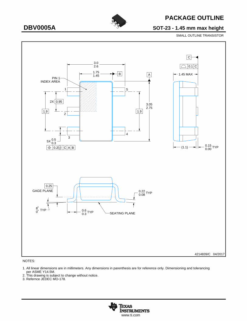
PACKAGE OUTLINE
C
TYP0.220.08
0.25
3.02.6
2X 0.95
1.9
1.45 MAX
TYP0.150.00
5X 0.50.3
TYP0.60.3
TYP80
1.9
A
3.052.75
B1.751.45
(1.1)
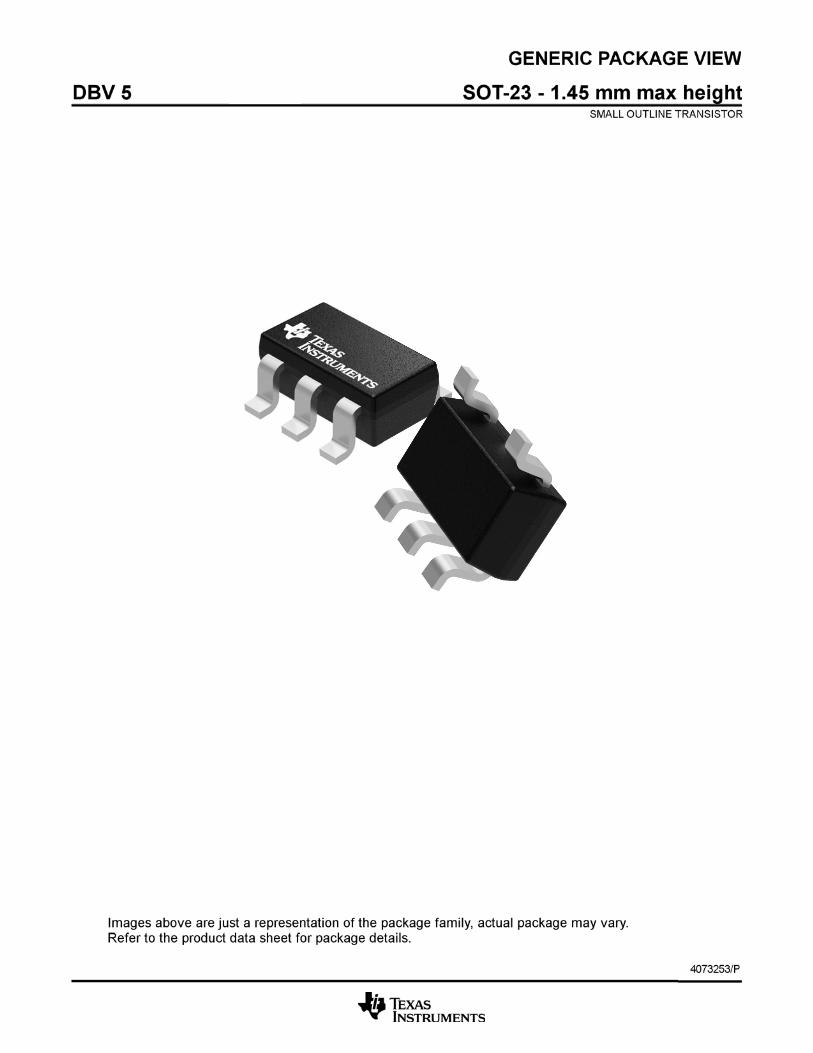
SOT-23 - 1.45 mm max heightDBV0005ASMALL OUTLINE TRANSISTOR
4214839/C 04/2017
NOTES: 1. All linear dimensions are in millimeters. Any dimensions in parenthesis are for reference only. Dimensioning and tolerancing per ASME Y14.5M.2. This drawing is subject to change without notice.3. Refernce JEDEC MO-178.
0.2 C A B
1
34
5
2
INDEX AREAPIN 1
GAGE PLANE
SEATING PLANE
0.1 C
SCALE 4.000

www.ti.com
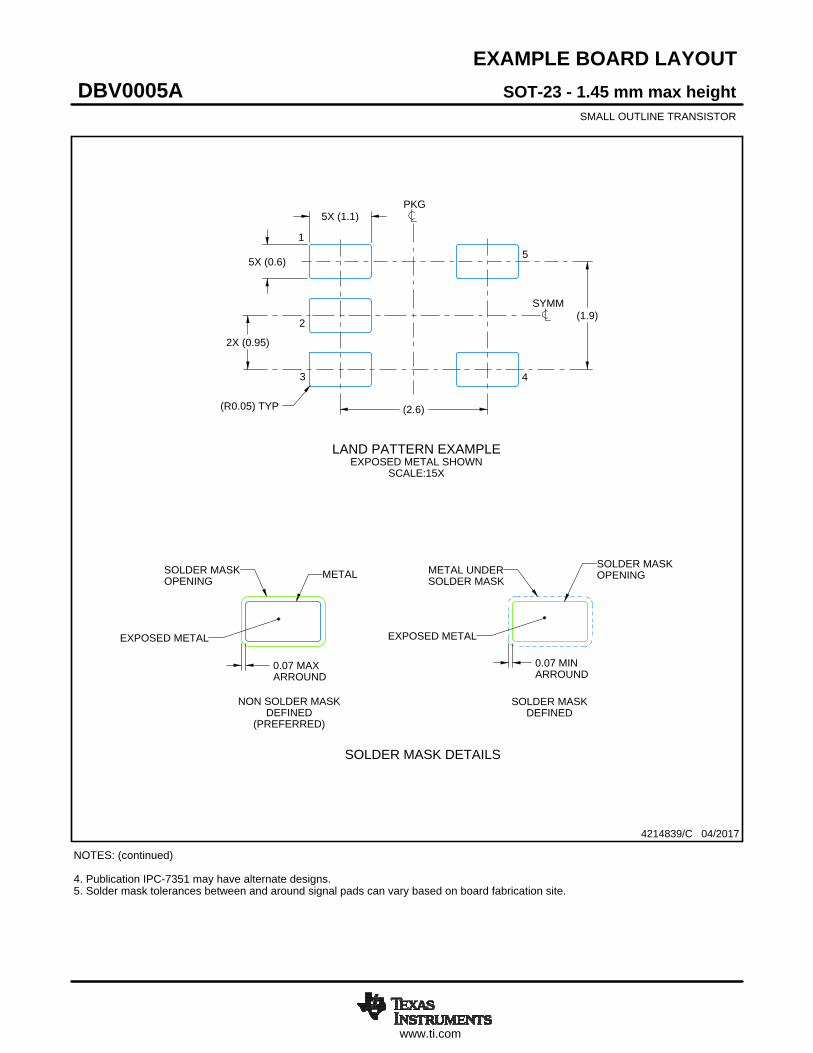
EXAMPLE BOARD LAYOUT
0.07 MAXARROUND
0.07 MINARROUND
5X (1.1)
5X (0.6)
(2.6)
(1.9)
2X (0.95)
(R0.05) TYP
4214839/C 04/2017
SOT-23 - 1.45 mm max heightDBV0005ASMALL OUTLINE TRANSISTOR
NOTES: (continued) 4. Publication IPC-7351 may have alternate designs. 5. Solder mask tolerances between and around signal pads can vary based on board fabrication site.
SYMM
LAND PATTERN EXAMPLEEXPOSED METAL SHOWN
SCALE:15X
PKG
1
3 4
5
2
SOLDER MASKOPENINGMETAL UNDER
SOLDER MASK
SOLDER MASKDEFINED
EXPOSED METAL
METALSOLDER MASKOPENING
NON SOLDER MASKDEFINED
(PREFERRED)
SOLDER MASK DETAILS
EXPOSED METAL
www.ti.com
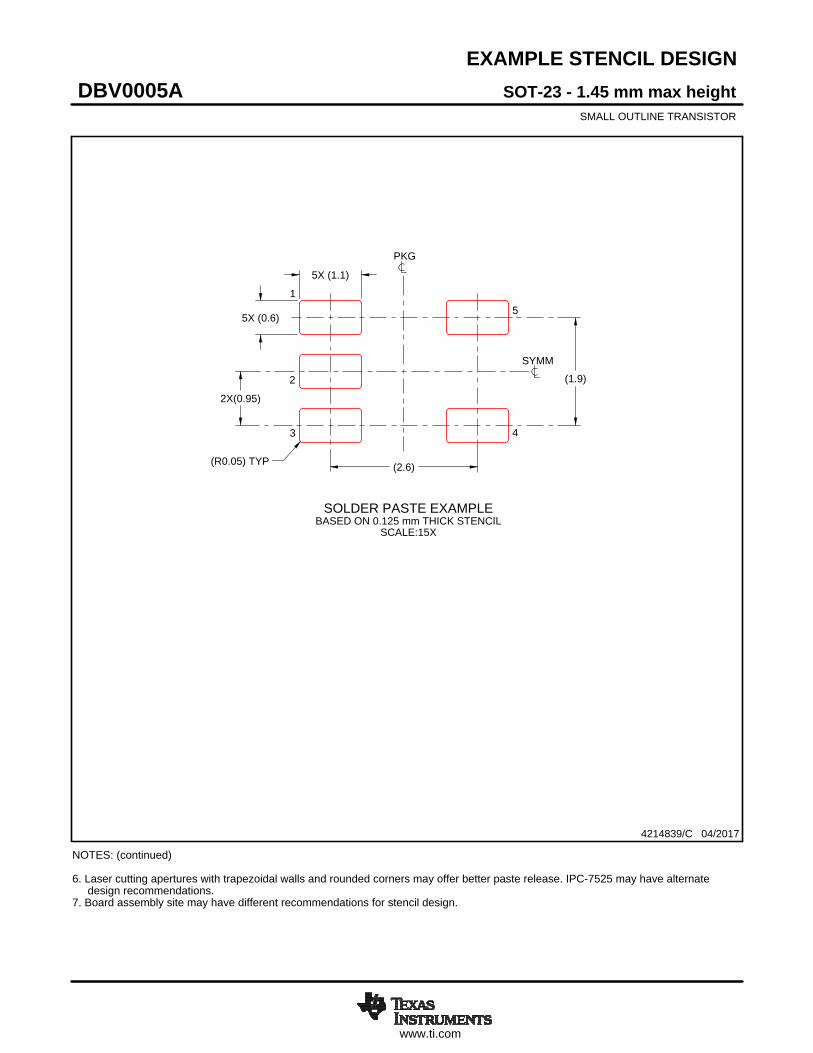
EXAMPLE STENCIL DESIGN
(2.6)
(1.9)
2X(0.95)
5X (1.1)
5X (0.6)
(R0.05) TYP
SOT-23 - 1.45 mm max heightDBV0005ASMALL OUTLINE TRANSISTOR
4214839/C 04/2017
NOTES: (continued) 6. Laser cutting apertures with trapezoidal walls and rounded corners may offer better paste release. IPC-7525 may have alternate design recommendations. 7. Board assembly site may have different recommendations for stencil design.
SOLDER PASTE EXAMPLEBASED ON 0.125 mm THICK STENCIL
SCALE:15X
SYMM
PKG
1
3 4
5
2
www.ti.com
PACKAGE OUTLINE
C
TYP0.220.08
0.25
3.02.6
2X 0.95
1.9
1.45 MAX
TYP0.150.00
5X 0.50.3
TYP0.60.3
TYP80
1.9
A
3.052.75
B1.751.45
(1.1)
SOT-23 - 1.45 mm max heightDBV0005ASMALL OUTLINE TRANSISTOR
4214839/C 04/2017
NOTES: 1. All linear dimensions are in millimeters. Any dimensions in parenthesis are for reference only. Dimensioning and tolerancing per ASME Y14.5M.2. This drawing is subject to change without notice.3. Refernce JEDEC MO-178.
0.2 C A B
1
34
5
2
INDEX AREAPIN 1
GAGE PLANE
SEATING PLANE
0.1 C
SCALE 4.000
www.ti.com
EXAMPLE BOARD LAYOUT
0.07 MAXARROUND
0.07 MINARROUND
5X (1.1)
5X (0.6)
(2.6)
(1.9)
2X (0.95)
(R0.05) TYP
4214839/C 04/2017
SOT-23 - 1.45 mm max heightDBV0005ASMALL OUTLINE TRANSISTOR
NOTES: (continued) 4. Publication IPC-7351 may have alternate designs. 5. Solder mask tolerances between and around signal pads can vary based on board fabrication site.
SYMM
LAND PATTERN EXAMPLEEXPOSED METAL SHOWN
SCALE:15X
PKG
1
3 4
5
2
SOLDER MASKOPENINGMETAL UNDER
SOLDER MASK
SOLDER MASKDEFINED
EXPOSED METAL
METALSOLDER MASKOPENING
NON SOLDER MASKDEFINED
(PREFERRED)
SOLDER MASK DETAILS
EXPOSED METAL

www.ti.com
EXAMPLE STENCIL DESIGN
(2.6)
(1.9)
2X(0.95)
5X (1.1)
5X (0.6)
(R0.05) TYP
SOT-23 - 1.45 mm max heightDBV0005ASMALL OUTLINE TRANSISTOR
4214839/C 04/2017
NOTES: (continued) 6. Laser cutting apertures with trapezoidal walls and rounded corners may offer better paste release. IPC-7525 may have alternate design recommendations. 7. Board assembly site may have different recommendations for stencil design.
SOLDER PASTE EXAMPLEBASED ON 0.125 mm THICK STENCIL
SCALE:15X
SYMM
PKG
1
3 4
5
2
IMPORTANT NOTICE
Texas Instruments Incorporated (TI) reserves the right to make corrections, enhancements, improvements and other changes to itssemiconductor products and services per JESD46, latest issue, and to discontinue any product or service per JESD48, latest issue. Buyersshould obtain the latest relevant information before placing orders and should verify that such information is current and complete.TI’s published terms of sale for semiconductor products (http://www.ti.com/sc/docs/stdterms.htm) apply to the sale of packaged integratedcircuit products that TI has qualified and released to market. Additional terms may apply to the use or sale of other types of TI products andservices.Reproduction of significant portions of TI information in TI data sheets is permissible only if reproduction is without alteration and isaccompanied by all associated warranties, conditions, limitations, and notices. TI is not responsible or liable for such reproduceddocumentation. Information of third parties may be subject to additional restrictions. Resale of TI products or services with statementsdifferent from or beyond the parameters stated by TI for that product or service voids all express and any implied warranties for theassociated TI product or service and is an unfair and deceptive business practice. TI is not responsible or liable for any such statements.Buyers and others who are developing systems that incorporate TI products (collectively, “Designers”) understand and agree that Designersremain responsible for using their independent analysis, evaluation and judgment in designing their applications and that Designers havefull and exclusive responsibility to assure the safety of Designers' applications and compliance of their applications (and of all TI productsused in or for Designers’ applications) with all applicable regulations, laws and other applicable requirements. Designer represents that, withrespect to their applications, Designer has all the necessary expertise to create and implement safeguards that (1) anticipate dangerousconsequences of failures, (2) monitor failures and their consequences, and (3) lessen the likelihood of failures that might cause harm andtake appropriate actions. Designer agrees that prior to using or distributing any applications that include TI products, Designer willthoroughly test such applications and the functionality of such TI products as used in such applications.TI’s provision of technical, application or other design advice, quality characterization, reliability data or other services or information,including, but not limited to, reference designs and materials relating to evaluation modules, (collectively, “TI Resources”) are intended toassist designers who are developing applications that incorporate TI products; by downloading, accessing or using TI Resources in anyway, Designer (individually or, if Designer is acting on behalf of a company, Designer’s company) agrees to use any particular TI Resourcesolely for this purpose and subject to the terms of this Notice.TI’s provision of TI Resources does not expand or otherwise alter TI’s applicable published warranties or warranty disclaimers for TIproducts, and no additional obligations or liabilities arise from TI providing such TI Resources. TI reserves the right to make corrections,enhancements, improvements and other changes to its TI Resources. TI has not conducted any testing other than that specificallydescribed in the published documentation for a particular TI Resource.Designer is authorized to use, copy and modify any individual TI Resource only in connection with the development of applications thatinclude the TI product(s) identified in such TI Resource. NO OTHER LICENSE, EXPRESS OR IMPLIED, BY ESTOPPEL OR OTHERWISETO ANY OTHER TI INTELLECTUAL PROPERTY RIGHT, AND NO LICENSE TO ANY TECHNOLOGY OR INTELLECTUAL PROPERTYRIGHT OF TI OR ANY THIRD PARTY IS GRANTED HEREIN, including but not limited to any patent right, copyright, mask work right, orother intellectual property right relating to any combination, machine, or process in which TI products or services are used. Informationregarding or referencing third-party products or services does not constitute a license to use such products or services, or a warranty orendorsement thereof. Use of TI Resources may require a license from a third party under the patents or other intellectual property of thethird party, or a license from TI under the patents or other intellectual property of TI.TI RESOURCES ARE PROVIDED “AS IS” AND WITH ALL FAULTS. TI DISCLAIMS ALL OTHER WARRANTIES ORREPRESENTATIONS, EXPRESS OR IMPLIED, REGARDING RESOURCES OR USE THEREOF, INCLUDING BUT NOT LIMITED TOACCURACY OR COMPLETENESS, TITLE, ANY EPIDEMIC FAILURE WARRANTY AND ANY IMPLIED WARRANTIES OFMERCHANTABILITY, FITNESS FOR A PARTICULAR PURPOSE, AND NON-INFRINGEMENT OF ANY THIRD PARTY INTELLECTUALPROPERTY RIGHTS. TI SHALL NOT BE LIABLE FOR AND SHALL NOT DEFEND OR INDEMNIFY DESIGNER AGAINST ANY CLAIM,INCLUDING BUT NOT LIMITED TO ANY INFRINGEMENT CLAIM THAT RELATES TO OR IS BASED ON ANY COMBINATION OFPRODUCTS EVEN IF DESCRIBED IN TI RESOURCES OR OTHERWISE. IN NO EVENT SHALL TI BE LIABLE FOR ANY ACTUAL,DIRECT, SPECIAL, COLLATERAL, INDIRECT, PUNITIVE, INCIDENTAL, CONSEQUENTIAL OR EXEMPLARY DAMAGES INCONNECTION WITH OR ARISING OUT OF TI RESOURCES OR USE THEREOF, AND REGARDLESS OF WHETHER TI HAS BEENADVISED OF THE POSSIBILITY OF SUCH DAMAGES.Unless TI has explicitly designated an individual product as meeting the requirements of a particular industry standard (e.g., ISO/TS 16949and ISO 26262), TI is not responsible for any failure to meet such industry standard requirements.Where TI specifically promotes products as facilitating functional safety or as compliant with industry functional safety standards, suchproducts are intended to help enable customers to design and create their own applications that meet applicable functional safety standardsand requirements. Using products in an application does not by itself establish any safety features in the application. Designers mustensure compliance with safety-related requirements and standards applicable to their applications. Designer may not use any TI products inlife-critical medical equipment unless authorized officers of the parties have executed a special contract specifically governing such use.Life-critical medical equipment is medical equipment where failure of such equipment would cause serious bodily injury or death (e.g., lifesupport, pacemakers, defibrillators, heart pumps, neurostimulators, and implantables). Such equipment includes, without limitation, allmedical devices identified by the U.S. Food and Drug Administration as Class III devices and equivalent classifications outside the U.S.TI may expressly designate certain products as completing a particular qualification (e.g., Q100, Military Grade, or Enhanced Product).Designers agree that it has the necessary expertise to select the product with the appropriate qualification designation for their applicationsand that proper product selection is at Designers’ own risk. Designers are solely responsible for compliance with all legal and regulatoryrequirements in connection with such selection.Designer will fully indemnify TI and its representatives against any damages, costs, losses, and/or liabilities arising out of Designer’s non-compliance with the terms and provisions of this Notice.
Mailing Address: Texas Instruments, Post Office Box 655303, Dallas, Texas 75265Copyright © 2018, Texas Instruments Incorporated