Embed Size (px)
Citation preview
LM4940
www.ti.com SNAS219C –OCTOBER 2003–REVISED MAY 2013
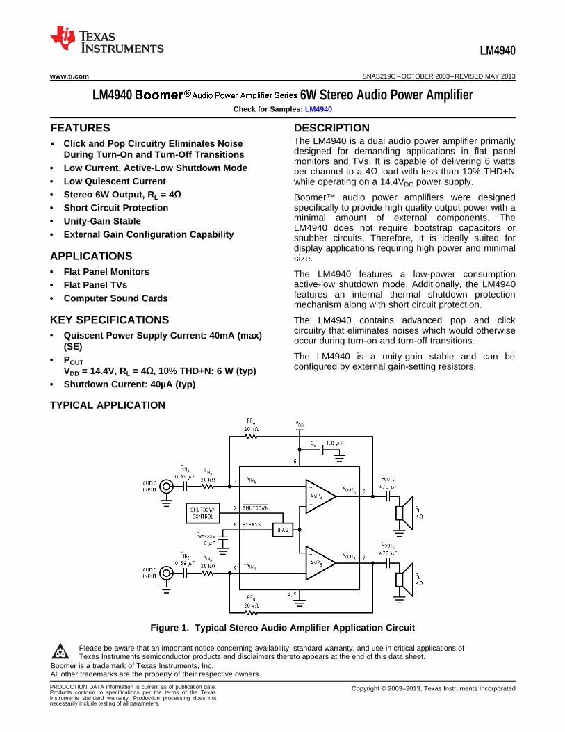
LM4940 6W Stereo Audio Power AmplifierCheck for Samples: LM4940
1FEATURES DESCRIPTIONThe LM4940 is a dual audio power amplifier primarily
23• Click and Pop Circuitry Eliminates Noisedesigned for demanding applications in flat panelDuring Turn-On and Turn-Off Transitionsmonitors and TVs. It is capable of delivering 6 watts
• Low Current, Active-Low Shutdown Mode per channel to a 4Ω load with less than 10% THD+N• Low Quiescent Current while operating on a 14.4VDC power supply.• Stereo 6W Output, RL = 4Ω Boomer™ audio power amplifiers were designed
specifically to provide high quality output power with a• Short Circuit Protectionminimal amount of external components. The• Unity-Gain StableLM4940 does not require bootstrap capacitors or
• External Gain Configuration Capability snubber circuits. Therefore, it is ideally suited fordisplay applications requiring high power and minimal
APPLICATIONS size.• Flat Panel Monitors The LM4940 features a low-power consumption
active-low shutdown mode. Additionally, the LM4940• Flat Panel TVsfeatures an internal thermal shutdown protection• Computer Sound Cardsmechanism along with short circuit protection.
The LM4940 contains advanced pop and clickKEY SPECIFICATIONScircuitry that eliminates noises which would otherwise• Quiscent Power Supply Current: 40mA (max) occur during turn-on and turn-off transitions.
(SE)The LM4940 is a unity-gain stable and can be• POUT configured by external gain-setting resistors.VDD = 14.4V, RL = 4Ω, 10% THD+N: 6 W (typ)
• Shutdown Current: 40µA (typ)
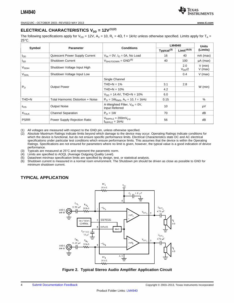
TYPICAL APPLICATION
Figure 1. Typical Stereo Audio Amplifier Application Circuit1
Please be aware that an important notice concerning availability, standard warranty, and use in critical applications ofTexas Instruments semiconductor products and disclaimers thereto appears at the end of this data sheet.
2Boomer is a trademark of Texas Instruments, Inc.3All other trademarks are the property of their respective owners.
PRODUCTION DATA information is current as of publication date. Copyright © 2003–2013, Texas Instruments IncorporatedProducts conform to specifications per the terms of the TexasInstruments standard warranty. Production processing does notnecessarily include testing of all parameters.
LM4940
SNAS219C –OCTOBER 2003–REVISED MAY 2013 www.ti.com
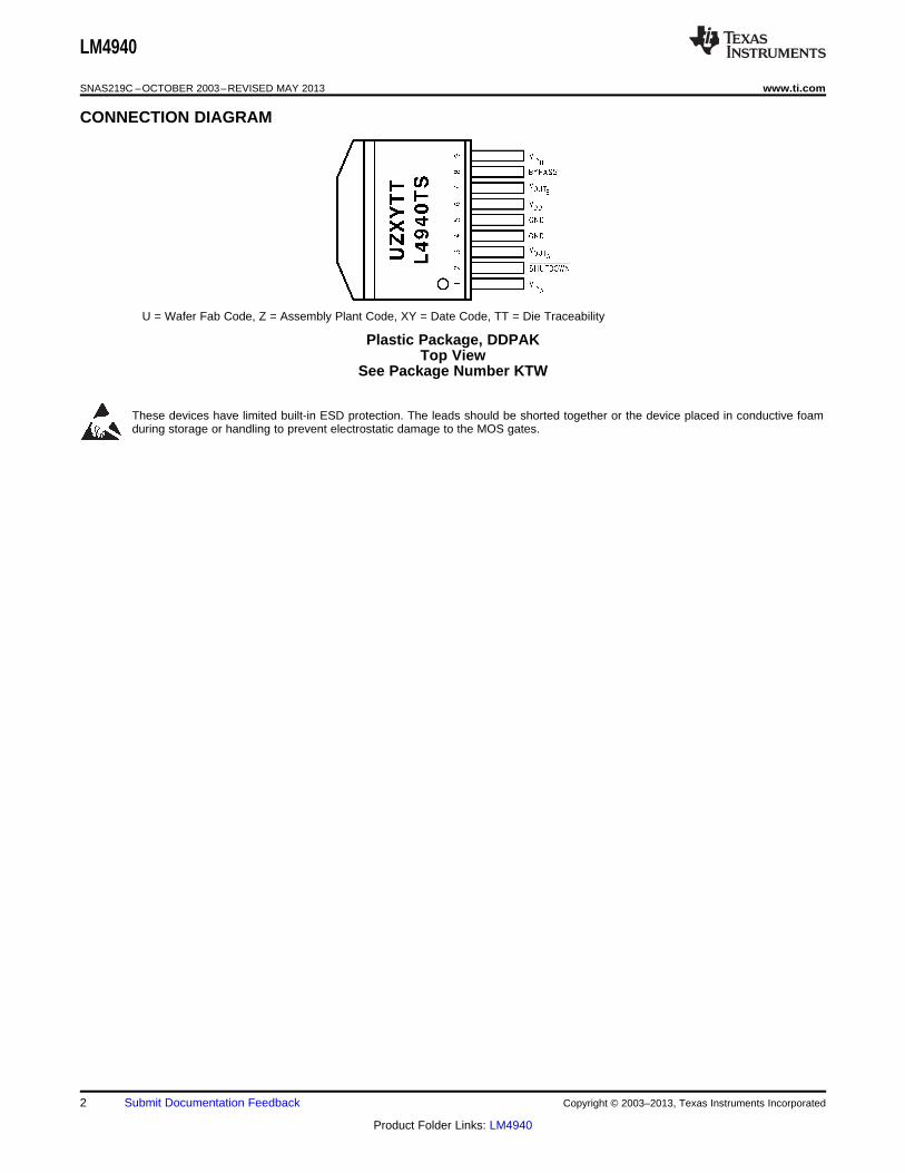
CONNECTION DIAGRAM
U = Wafer Fab Code, Z = Assembly Plant Code, XY = Date Code, TT = Die Traceability
Plastic Package, DDPAKTop View
See Package Number KTW
These devices have limited built-in ESD protection. The leads should be shorted together or the device placed in conductive foamduring storage or handling to prevent electrostatic damage to the MOS gates.
2 Submit Documentation Feedback Copyright © 2003–2013, Texas Instruments Incorporated
Product Folder Links: LM4940
LM4940
www.ti.com SNAS219C –OCTOBER 2003–REVISED MAY 2013
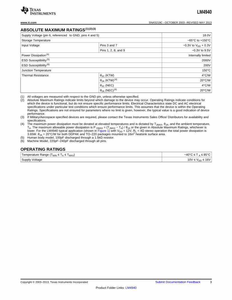
ABSOLUTE MAXIMUM RATINGS (1) (2) (3)
Supply Voltage (pin 6, referenced to GND, pins 4 and 5) 18.0V
Storage Temperature −65°C to +150°C
Input Voltage Pins 3 and 7 −0.3V to VDD + 0.3V
Pins 1, 2, 8, and 9 −0.3V to 9.5V
Power Dissipation (4) Internally limited
ESD Susceptibility (5) 2000V
ESD Susceptibility (6) 200V
Junction Temperature 150°C
Thermal Resistance θJC (KTW) 4°C/W
θJA (KTW) (4) 20°C/W
θJC (NEC) 4°C/W
θJA (NEC) (4) 20°C/W
(1) All voltages are measured with respect to the GND pin, unless otherwise specified.(2) Absolute Maximum Ratings indicate limits beyond which damage to the device may occur. Operating Ratings indicate conditions for
which the device is functional, but do not ensure specific performance limits. Electrical Characteristics state DC and AC electricalspecifications under particular test conditions which ensure performance limits. This assumes that the device is within the OperatingRatings. Specifications are not ensured for parameters where no limit is given, however, the typical value is a good indication of deviceperformance.
(3) If Military/Aerospace specified devices are required, please contact the Texas Instruments Sales Office/ Distributors for availability andspecifications.
(4) The maximum power dissipation must be derated at elevated temperatures and is dictated by TJMAX, θJA, and the ambient temperature,TA. The maximum allowable power dissipation is P DMAX = (TJMAX − TA) / θJA or the given in Absolute Maximum Ratings, whichever islower. For the LM4940 typical application (shown in Figure 1) with VDD = 12V, RL = 4Ω stereo operation the total power dissipation is3.65W. θJA = 20°C/W for both DDPAK and TO–220 packages mounted to 16in2 heatsink surface area.
(5) Human body model, 100pF discharged through a 1.5kΩ resistor.(6) Machine Model, 220pF–240pF discharged through all pins.
OPERATING RATINGSTemperature Range (TMIN ≤ TA ≤ TMAX) −40°C ≤ T A ≤ 85°C
Supply Voltage 10V ≤ VDD ≤ 16V
Copyright © 2003–2013, Texas Instruments Incorporated Submit Documentation Feedback 3
Product Folder Links: LM4940
LM4940
SNAS219C –OCTOBER 2003–REVISED MAY 2013 www.ti.com
ELECTRICAL CHARACTERISTICS VDD = 12V (1) (2)
The following specifications apply for VDD = 12V, AV = 10, RL = 4Ω, f = 1kHz unless otherwise specified. Limits apply for TA =25°C.
LM4940 UnitsSymbol Parameter Conditions (Limits)Typical (3) Limit (4) (5)
IDD Quiescent Power Supply Current VIN = 0V, IO = 0A, No Load 16 40 mA (max)
ISD Shutdown Current VSHUTDOWN = GND (6) 40 100 µA (max)
2.0 V (min)VSDIH Shutdown Voltage Input High VDD/2 V (max)
VSDIL Shutdown Voltage Input Low 0.4 V (max)
Single Channel
THD+N = 1% 3.1 2.8PO Output Power W (min)
THD+N = 10% 4.2
VDD = 14.4V, THD+N = 10% 6.0
THD+N Total Harmomic Distortion + Noise PO = 1WRMS, AV = 10, f = 1kHz 0.15 %
A-Weighted Filter, VIN = 0V,εOS Output Noise 10 µVInput Referred
XTALK Channel Separation PO = 1W 70 dB
VRIPPLE = 200mVp-pPSRR Power Supply Rejection Ratio 56 dBfRIPPLE = 1kHz
(1) All voltages are measured with respect to the GND pin, unless otherwise specified.(2) Absolute Maximum Ratings indicate limits beyond which damage to the device may occur. Operating Ratings indicate conditions for
which the device is functional, but do not ensure specific performance limits. Electrical Characteristics state DC and AC electricalspecifications under particular test conditions which ensure performance limits. This assumes that the device is within the OperatingRatings. Specifications are not ensured for parameters where no limit is given, however, the typical value is a good indication of deviceperformance.
(3) Typicals are measured at 25°C and represent the parametric norm.(4) Limits are specified to AOQL (Average Outgoing Quality Level).(5) Datasheet min/max specification limits are specified by design, test, or statistical analysis.(6) Shutdown current is measured in a normal room environment. The Shutdown pin should be driven as close as possible to GND for
minimum shutdown current.
TYPICAL APPLICATION
Figure 2. Typical Stereo Audio Amplifier Application Circuit
4 Submit Documentation Feedback Copyright © 2003–2013, Texas Instruments Incorporated
Product Folder Links: LM4940

LM4940
www.ti.com SNAS219C –OCTOBER 2003–REVISED MAY 2013
EXTERNAL COMPONENTS DESCRIPTION
Refer to Figure 1.
Components Functional Description
This is the inverting input resistance that, along with RF, sets the closed-loop gain. Input resistance RIN and input1. RIN capacitance CIN form a high pass filter.
The filter's cutoff frequency is fC = 1/(2πRINCIN).
This is the input coupling capacitor. It blocks DC voltage at the amplifier's inverting input. CIN and RIN create a2. CIN highpass filter. The filter's cutoff frequency is fC = 1/(2πRINCIN). Refer to the SELECTING EXTERNAL
COMPONENTS section for an explanation of determining CIN's value.
3. RF This is the feedback resistance that, along with Ri, sets closed-loop gain.
The supply bypass capacitor. Refer to the POWER SUPPLY BYPASSING section for information about properly4. CS placing, and selecting the value of, this capacitor.
This capacitor filters the half-supply voltage present on the BYPASS pin. Refer to the SELECTING EXTERNAL5. CBYPASS COMPONENTS for information about properly placing, and selecting the value of, this capacitor.
This is the output coupling capacitor. It blocks the nominal VDD/2 voltage present at the output and prevents it6. COUT from reaching the load. COUT and RL form a high pass filter whose cutoff frequency is fC = 1/(2πRLCOUT). Refer to
the SELECTING EXTERNAL COMPONENTS section for an explanation of determining COUT's value.
Copyright © 2003–2013, Texas Instruments Incorporated Submit Documentation Feedback 5
Product Folder Links: LM4940
LM4940
SNAS219C –OCTOBER 2003–REVISED MAY 2013 www.ti.com
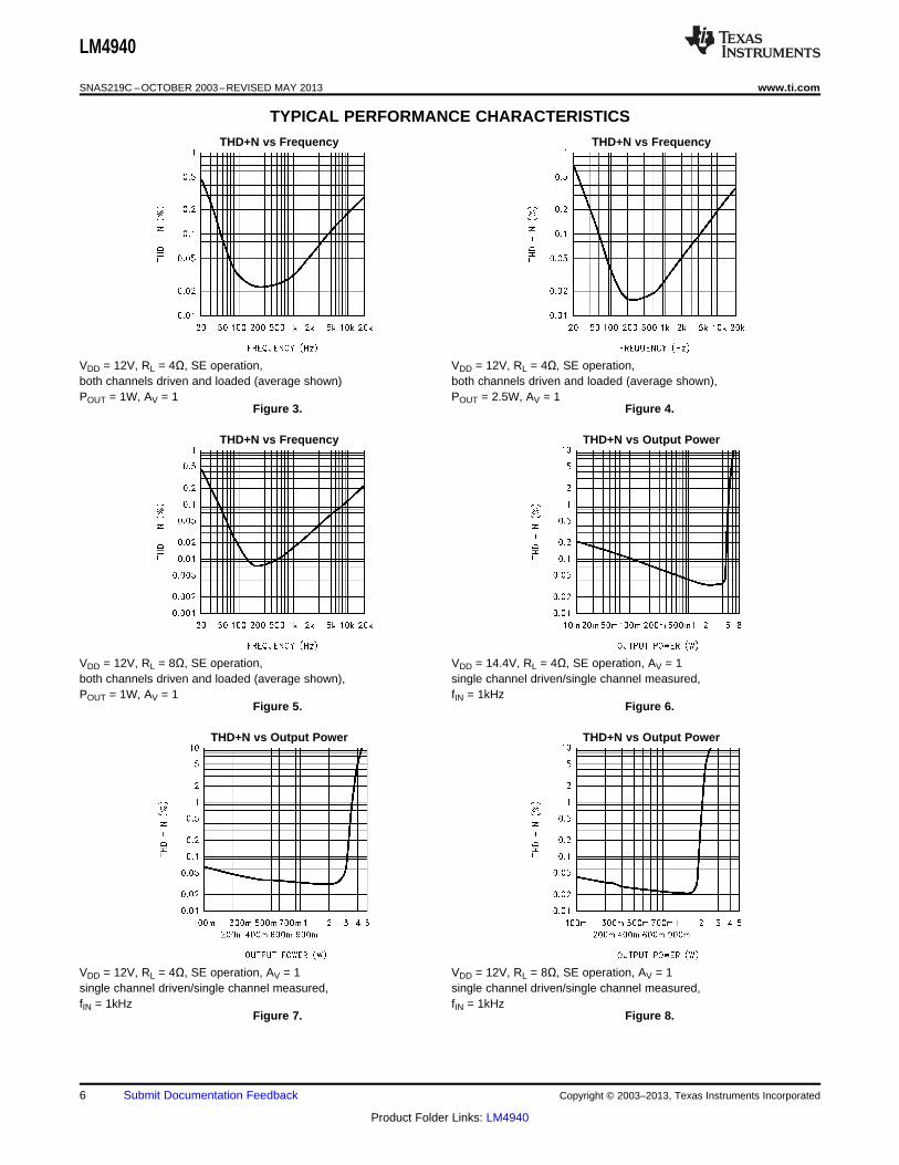
TYPICAL PERFORMANCE CHARACTERISTICS
THD+N vs Frequency THD+N vs Frequency
VDD = 12V, RL = 4Ω, SE operation, VDD = 12V, RL = 4Ω, SE operation,both channels driven and loaded (average shown) both channels driven and loaded (average shown),POUT = 1W, AV = 1 POUT = 2.5W, AV = 1
Figure 3. Figure 4.
THD+N vs Frequency THD+N vs Output Power
VDD = 12V, RL = 8Ω, SE operation, VDD = 14.4V, RL = 4Ω, SE operation, AV = 1both channels driven and loaded (average shown), single channel driven/single channel measured,POUT = 1W, AV = 1 fIN = 1kHz
Figure 5. Figure 6.
THD+N vs Output Power THD+N vs Output Power
VDD = 12V, RL = 4Ω, SE operation, AV = 1 VDD = 12V, RL = 8Ω, SE operation, AV = 1single channel driven/single channel measured, single channel driven/single channel measured,fIN = 1kHz fIN = 1kHz
Figure 7. Figure 8.
6 Submit Documentation Feedback Copyright © 2003–2013, Texas Instruments Incorporated
Product Folder Links: LM4940
LM4940
www.ti.com SNAS219C –OCTOBER 2003–REVISED MAY 2013
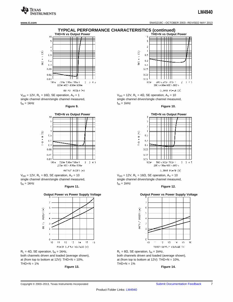
TYPICAL PERFORMANCE CHARACTERISTICS (continued)THD+N vs Output Power THD+N vs Output Power
VDD = 12V, RL = 16Ω, SE operation, AV = 1 VDD = 12V, RL = 4Ω, SE operation, AV = 10single channel driven/single channel measured, single channel driven/single channel measured,fIN = 1kHz fIN = 1kHz
Figure 9. Figure 10.
THD+N vs Output Power THD+N vs Output Power
VDD = 12V, RL = 8Ω, SE operation, AV = 10 VDD = 12V, RL = 16Ω, SE operation, AV = 10single channel driven/single channel measured, single channel driven/single channel measured,fIN = 1kHz fIN = 1kHz
Figure 11. Figure 12.
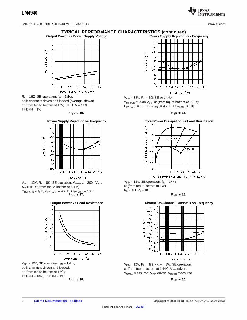
Output Power vs Power Supply Voltage Output Power vs Power Supply Voltage
RL = 4Ω, SE operation, fIN = 1kHz, RL = 8Ω, SE operation, fIN = 1kHz,both channels driven and loaded (average shown), both channels driven and loaded (average shown),at (from top to bottom at 12V): THD+N = 10%, at (from top to bottom at 12V): THD+N = 10%,THD+N = 1% THD+N = 1%
Figure 13. Figure 14.
Copyright © 2003–2013, Texas Instruments Incorporated Submit Documentation Feedback 7
Product Folder Links: LM4940
LM4940
SNAS219C –OCTOBER 2003–REVISED MAY 2013 www.ti.com
TYPICAL PERFORMANCE CHARACTERISTICS (continued)Output Power vs Power Supply Voltage Power Supply Rejection vs Frequency
RL = 16Ω, SE operation, fIN = 1kHz, VDD = 12V, RL = 8Ω, SE operation,both channels driven and loaded (average shown), VRIPPLE = 200mVp-p, at (from top to bottom at 60Hz):at (from top to bottom at 12V): THD+N = 10%, CBYPASS = 1µF, CBYPASS = 4.7µF, CBYPASS = 10µFTHD+N = 1%
Figure 15. Figure 16.
Power Supply Rejection vs Frequency Total Power Dissipation vs Load Dissipation
VDD = 12V, SE operation, fIN = 1kHz,VDD = 12V, RL = 8Ω, SE operation, VRIPPLE = 200mVp-p,at (from top to bottom at 1W):AV = 10, at (from top to bottom at 60Hz):RL = 4Ω, RL = 8ΩCBYPASS = 1µF, CBYPASS = 4.7µF, CBYPASS = 10µF
Figure 17. Figure 18.
Output Power vs Load Resistance Channel-to-Channel Crosstalk vs Frequency
VDD = 12V, SE operation, fIN = 1kHz, VDD = 12V, RL = 4Ω, POUT = 1W, SE operation,both channels driven and loaded, at (from top to bottom at 1kHz): VINB driven,at (from top to bottom at 15Ω): VOUTA measured; VINA driven, VOUTB measuredTHD+N = 10%, THD+N = 1%
Figure 19. Figure 20.
8 Submit Documentation Feedback Copyright © 2003–2013, Texas Instruments Incorporated
Product Folder Links: LM4940
LM4940
www.ti.com SNAS219C –OCTOBER 2003–REVISED MAY 2013
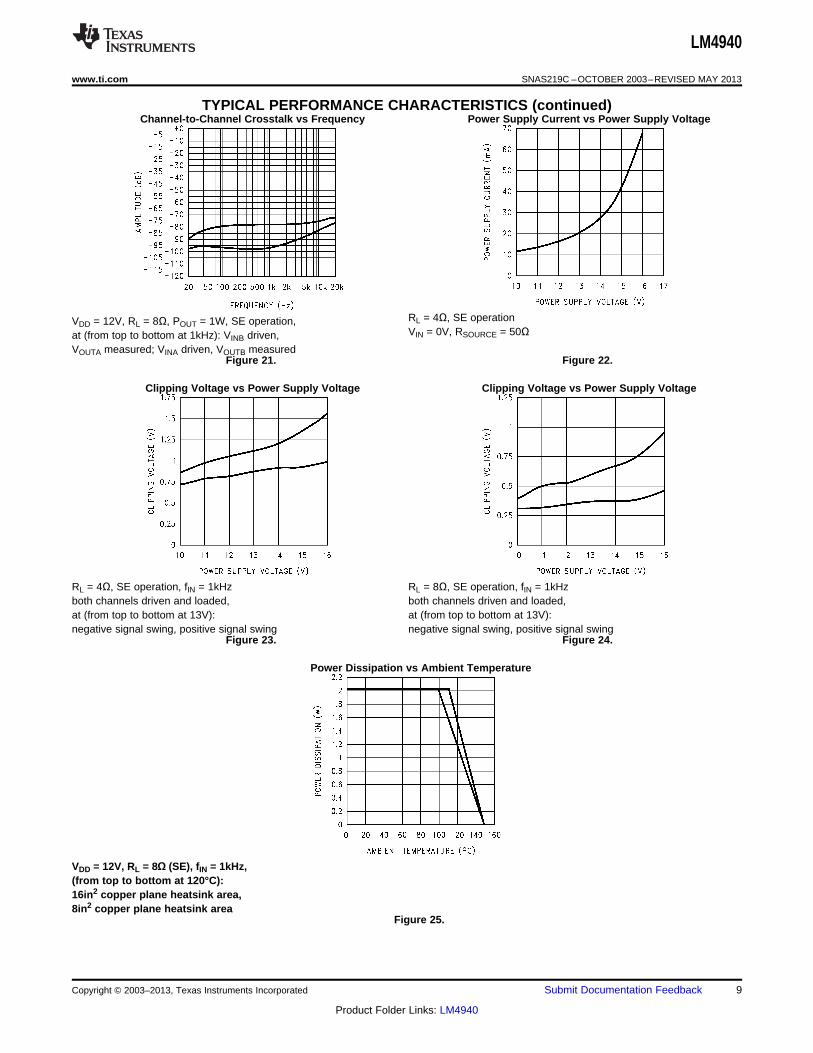
TYPICAL PERFORMANCE CHARACTERISTICS (continued)Channel-to-Channel Crosstalk vs Frequency Power Supply Current vs Power Supply Voltage
RL = 4Ω, SE operationVDD = 12V, RL = 8Ω, POUT = 1W, SE operation,VIN = 0V, RSOURCE = 50Ωat (from top to bottom at 1kHz): VINB driven,
VOUTA measured; VINA driven, VOUTB measuredFigure 21. Figure 22.
Clipping Voltage vs Power Supply Voltage Clipping Voltage vs Power Supply Voltage
RL = 4Ω, SE operation, fIN = 1kHz RL = 8Ω, SE operation, fIN = 1kHzboth channels driven and loaded, both channels driven and loaded,at (from top to bottom at 13V): at (from top to bottom at 13V):negative signal swing, positive signal swing negative signal swing, positive signal swing
Figure 23. Figure 24.
Power Dissipation vs Ambient Temperature
VDD = 12V, RL = 8Ω (SE), fIN = 1kHz,(from top to bottom at 120°C):16in2 copper plane heatsink area,8in2 copper plane heatsink area
Figure 25.
Copyright © 2003–2013, Texas Instruments Incorporated Submit Documentation Feedback 9
Product Folder Links: LM4940

LM4940
SNAS219C –OCTOBER 2003–REVISED MAY 2013 www.ti.com
APPLICATION INFORMATION
Figure 26. Typical LM4940 Stereo Amplifier Application Circuit
HIGH VOLTAGE BOOMER WITH INCREASED OUTPUT POWER
Unlike previous 5V Boomer amplifiers, the LM4940 is designed to operate over a power supply voltages range of10V to 15V. Operating on a 12V power supply, the LM4940 will deliver 3.1W per channel into 4Ω loads with nomore than 1% THD+N.
POWER DISSIPATION
Power dissipation is a major concern when designing a successful single-ended amplifier. Equation 1 states themaximum power dissipation point for a single-ended amplifier operating at a given supply voltage and driving aspecified output load.
PDMAX-SE = (VDD) 2/ (2π2RL): Single Ended (1)
The LM4940's dissipation is twice the value given by Equation 1 when driving two SE loads. For a 12V supplyand two 8Ω SE loads, the LM4940's dissipation is 1.82W.
The maximum power dissipation point (twice the value given by Equation 1 must not exceed the powerdissipation given by Equation 2:
PDMAX' = (TJMAX - TA) / θJA (2)
The LM4940's TJMAX = 150°C. In the KTW package, the LM4940's θJA is 20°C/W when the metal tab is solderedto a copper plane of at least 16in2. This plane can be split between the top and bottom layers of a two-sidedPCB. Connect the two layers together under the tab with a 5x5 array of vias. For the NEC package, use anexternal heatsink with a thermal impedance that is less than 20°C/W. At any given ambient temperature TA, useEquation 3 to find the maximum internal power dissipation supported by the IC packaging. RearrangingEquation 3 and substituting PDMAX for PDMAX' results in Equation 4. This equation gives the maximum ambienttemperature that still allows maximum stereo power dissipation without violating the LM4940's maximum junctiontemperature.
10 Submit Documentation Feedback Copyright © 2003–2013, Texas Instruments Incorporated
Product Folder Links: LM4940
LM4940
www.ti.com SNAS219C –OCTOBER 2003–REVISED MAY 2013
TA = TJMAX - PDMAX-SEθJA (3)
For a typical application with a 12V power supply and two 4Ω SE loads, the maximum ambient temperature thatallows maximum stereo power dissipation without exceeding the maximum junction temperature is approximately113°C for the KTW package.
TJMAX = PDMAX-SEθJA + TA (4)
Equation 4 gives the maximum junction temperature TJMAX. If the result violates the LM4940's 150°C, reduce themaximum junction temperature by reducing the power supply voltage or increasing the load resistance. Furtherallowance should be made for increased ambient temperatures.
The above examples assume that a device is operating around the maximum power dissipation point. Sinceinternal power dissipation is a function of output power, higher ambient temperatures are allowed as outputpower or duty cycle decreases.
If the result of Equation 3 is greater than that of Equation 4, then decrease the supply voltage, increase the loadimpedance, or reduce the ambient temperature. Further, ensure that speakers rated at a nominal 4Ω do not fallbelow 3Ω. If these measures are insufficient, a heat sink can be added to reduce θJA. The heat sink can becreated using additional copper area around the package, with connections to the ground pins, supply pin andamplifier output pins. Refer to the TYPICAL PERFORMANCE CHARACTERISTICS curves for power dissipationinformation at lower output power levels.
POWER SUPPLY VOLTAGE LIMITS
Continuous proper operation is ensured by never exceeding the voltage applied to any pin, with respect toground, as listed in the Absolute Maximum Ratings section.
POWER SUPPLY BYPASSING
As with any power amplifier, proper supply bypassing is critical for low noise performance and high power supplyrejection. Applications that employ a voltage regulator typically use a 10µF in parallel with a 0.1µF filtercapacitors to stabilize the regulator's output, reduce noise on the supply line, and improve the supply's transientresponse. However, their presence does not eliminate the need for a local 1.0µF tantalum bypass capacitanceconnected between the LM4940's supply pins and ground. Do not substitute a ceramic capacitor for thetantalum. Doing so may cause oscillation. Keep the length of leads and traces that connect capacitors betweenthe LM4940's power supply pin and ground as short as possible. Connecting a 10µF capacitor, CBYPASS, betweenthe BYPASS pin and ground improves the internal bias voltage's stability and improves the amplifier's PSRR.The PSRR improvements increase as the bypass pin capacitor value increases. Too large, however, increasesturn-on time and can compromise the amplifier's click and pop performance. The selection of bypass capacitorvalues, especially CBYPASS, depends on desired PSRR requirements, click and pop performance (as explained inthe section, SELECTING EXTERNAL COMPONENTS), system cost, and size constraints.
MICRO-POWER SHUTDOWN
The LM4940 features an active-low shutdown mode that disables the amplifier's bias circuitry, reducing thesupply current to 40μA (typ). Connect SHUTDOWN to a voltage between 2V to VDD/2 for normal operation.Connect SHUTDOWN to GND to disable the device. A voltage that is greater than GND can increase shutdowncurrent.
Copyright © 2003–2013, Texas Instruments Incorporated Submit Documentation Feedback 11
Product Folder Links: LM4940
LM4940
SNAS219C –OCTOBER 2003–REVISED MAY 2013 www.ti.com
SELECTING EXTERNAL COMPONENTS
Input Capacitor Value Selection
Two quantities determine the value of the input coupling capacitor: the lowest audio frequency that requiresamplification and desired output transient suppression.
As shown in Figure 26, the input resistor (RIN) and the input capacitor (CIN) produce a high pass filter cutofffrequency that is found using Equation 5.
fC = 1/2πRiCi (5)
As an example when using a speaker with a low frequency limit of 50Hz, Ci, using Equation 5 is 0.159µF. The0.39µF CINA shown in Figure 26 allows the LM4940 to drive high efficiency, full range speaker whose responseextends below 30Hz.
Output Coupling Capacitor Value Selection
The capacitors COUTA and COUTB that block the VDD/2 output DC bias voltage and couple the output AC signal tothe amplifier loads also determine low frequency response. These capacitors, combined with their respectiveloads create a highpass filter cutoff frequency. The frequency is also given by Equation 5.
Using the same conditions as above, with a 4Ω speaker, COUT is 820µF (nearest common valve).
Bypass Capacitor Value
Besides minimizing the input capacitor size, careful consideration should be paid to value of CBYPASS, thecapacitor connected to the BYPASS pin. Since CBYPASS determines how fast the LM4940 settles to quiescentoperation, its value is critical when minimizing turn-on pops. The slower the LM4940's outputs ramp to theirquiescent DC voltage (nominally VDD/2), the smaller the turn-on pop. Choosing CBYPASS equal to 10µF along witha small value of CIN (in the range of 0.1µF to 0.39µF), produces a click-less and pop-less shutdown function. Asdiscussed above, choosing CIN no larger than necessary for the desired bandwidth helps minimize clicks andpops.
OPTIMIZING CLICK AND POP REDUCTION PERFORMANCE
The LM4940 contains circuitry that eliminates turn-on and shutdown transients ("clicks and pops"). For thisdiscussion, turn-on refers to either applying the power supply voltage or when the micro-power shutdown modeis deactivated.
As the VDD/2 voltage present at the BYPASS pin ramps to its final value, the LM4940's internal amplifiers areconfigured as unity gain buffers and are disconnected from the AMPA and AMPB pins. An internal current sourcecharges the capacitor connected between the BYPASS pin and GND in a controlled manner. Ideally, the inputand outputs track the voltage applied to the BYPASS pin. The gain of the internal amplifiers remains unity untilthe voltage applied to the BYPASS pin.
The gain of the internal amplifiers remains unity until the voltage on the bypass pin reaches VDD/2. As soon asthe voltage on the bypass pin is stable, the device becomes fully operational and the amplifier outputs arereconnected to their respective output pins. Although the BYPASS pin current cannot be modified, changing thesize of CBYPASS alters the device's turn-on time. Here are some typical turn-on times for various values ofCBYPASS:
CB (µF) TON (ms)
1.0 120
2.2 120
4.7 200
10 440
12 Submit Documentation Feedback Copyright © 2003–2013, Texas Instruments Incorporated
Product Folder Links: LM4940
LM4940
www.ti.com SNAS219C –OCTOBER 2003–REVISED MAY 2013
In order eliminate "clicks and pops", all capacitors must be discharged before turn-on. Rapidly switching VDD maynot allow the capacitors to fully discharge, which may cause "clicks and pops".
There is a relationship between the value of CIN and CBYPASS that ensures minimum output transient when poweris applied or the shutdown mode is deactivated. Best performance is achieved by setting the time constantcreated by CIN and Ri + Rf to a value less than the turn-on time for a given value of CBYPASS as shown in the tableabove.
AUDIO POWER AMPLIFIER DESIGN
Audio Amplifier Design: Driving 3W into a 4Ω load
The following are the desired operational parameters:
Power Output 3WRMS
Load Impedance 4ΩInput Level 0.3VRMS (max)
Input Impedance 20kΩBandwidth 100Hz–20kHz ± 0.25dB
The design begins by specifying the minimum supply voltage necessary to obtain the specified output power.One way to find the minimum supply voltage is to use the Output Power vs Power Supply Voltage curve in theTYPICAL PERFORMANCE CHARACTERISTICS section. Another way, using Equation 6, is to calculate thepeak output voltage necessary to achieve the desired output power for a given load impedance. To account forthe amplifier's dropout voltage, two additional voltages, based on the Clipping Dropout Voltage vs Power SupplyVoltage in the TYPICAL PERFORMANCE CHARACTERISTICS curves, must be added to the result obtained byEquation 6. The result is Equation 7.
(6)
VDD = VOUTPEAK + VODTOP + VODBOT (7)
The Figure 13 graph for an 8Ω load indicates a minimum supply voltage of 11.8V. The commonly used 12Vsupply voltage easily meets this. The additional voltage creates the benefit of headroom, allowing the LM4940 toproduce an output power of 3W without clipping or other audible distortion. The choice of supply voltage mustalso not create a situation that violates of maximum power dissipation as explained above in the POWERDISSIPATION section. After satisfying the LM4940's power dissipation requirements, the minimum differentialgain needed to achieve 3W dissipation in a 4Ω BTL load is found using Equation 8.
(8)
Thus, a minimum gain of 11.6 allows the LM4940's to reach full output swing and maintain low noise and THD+Nperformance. For this example, let AV = 12. The amplifier's overall BTL gain is set using the input (RINA) andfeedback (R) resistors of the first amplifier in the series BTL configuration. Additionaly, AV-BTL is twice the gain setby the first amplifier's RIN and Rf. With the desired input impedance set at 20kΩ, the feedback resistor is foundusing Equation 9.
Rf/ RIN = AV (9)
The value of Rf is 240kΩ. The nominal output power is 3W.
Copyright © 2003–2013, Texas Instruments Incorporated Submit Documentation Feedback 13
Product Folder Links: LM4940
LM4940
SNAS219C –OCTOBER 2003–REVISED MAY 2013 www.ti.com
The last step in this design example is setting the amplifier's -3dB frequency bandwidth. To achieve the desired±0.25dB pass band magnitude variation limit, the low frequency response must extend to at least one-fifth thelower bandwidth limit and the high frequency response must extend to at least five times the upper bandwidthlimit. The gain variation for both response limits is 0.17dB, well within the ±0.25dB-desired limit. The results arean
fL = 100Hz / 5 = 20Hz (10)
and
fL = 20kHz x 5 = 100kHz (11)
As mentioned in the SELECTING EXTERNAL COMPONENTS section, RINA and CINA, as well as COUT and RL,create a highpass filter that sets the amplifier's lower bandpass frequency limit. Find the coupling capacitor'svalue using Equation 14.
CIN = 1 / 2πRINfL (12)
The result is
1 / (2πx20kΩx20Hz) = 0.398µF = CIN (13)
and
1 / (2π x 4Ω x 20Hz) = 1989µF = COUT (14)
Use a 0.39µF capacitor for CIN and a 2000µF capacitor for COUT, the closest standard values.
The product of the desired high frequency cutoff (100kHz in this example) and the differential gain AV,determines the upper passband response limit. With AV = 12 and fH = 100kHz, the closed-loop gain bandwidthproduct (GBWP) is 1.2mHz. This is less than the LM4940's 3.5MHz GBWP. With this margin, the amplifier canbe used in designs that require more differential gain while avoiding performance restricting bandwidthlimitations.
RECOMMENDED PRINTED CIRCUIT BOARD LAYOUT
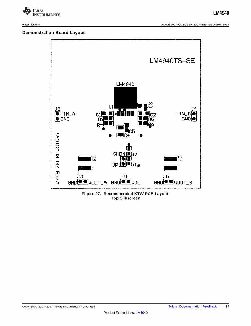
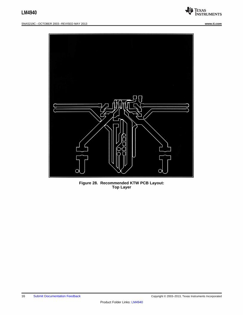
Figure 27 through Figure 29 show the recommended two-layer PC board layout that is optimized for the DDPAK-packaged LM4940 and associated external components. This circuit board is designed for use with an external12V supply and 4Ω (min) speakers.
This circuit board is easy to use. Apply 12V and ground to the board's VDD and GND pads, respectively. Connecta speaker between the board's OUTA and OUTB outputs and their respective GND terminals.
14 Submit Documentation Feedback Copyright © 2003–2013, Texas Instruments Incorporated
Product Folder Links: LM4940
LM4940
www.ti.com SNAS219C –OCTOBER 2003–REVISED MAY 2013
Demonstration Board Layout
Figure 27. Recommended KTW PCB Layout:Top Silkscreen
Copyright © 2003–2013, Texas Instruments Incorporated Submit Documentation Feedback 15
Product Folder Links: LM4940
LM4940
SNAS219C –OCTOBER 2003–REVISED MAY 2013 www.ti.com
Figure 28. Recommended KTW PCB Layout:Top Layer
16 Submit Documentation Feedback Copyright © 2003–2013, Texas Instruments Incorporated
Product Folder Links: LM4940
LM4940
www.ti.com SNAS219C –OCTOBER 2003–REVISED MAY 2013
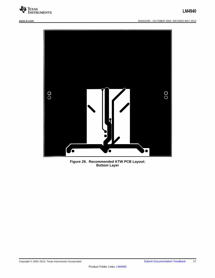
Figure 29. Recommended KTW PCB Layout:Bottom Layer
Copyright © 2003–2013, Texas Instruments Incorporated Submit Documentation Feedback 17
Product Folder Links: LM4940
LM4940
SNAS219C –OCTOBER 2003–REVISED MAY 2013 www.ti.com
REVISION HISTORY
Changes from Revision B (May 2013) to Revision C Page
• Changed layout of National Data Sheet to TI format .......................................................................................................... 17
18 Submit Documentation Feedback Copyright © 2003–2013, Texas Instruments Incorporated
Product Folder Links: LM4940
PACKAGE OPTION ADDENDUM
www.ti.com 3-May-2013
Addendum-Page 1
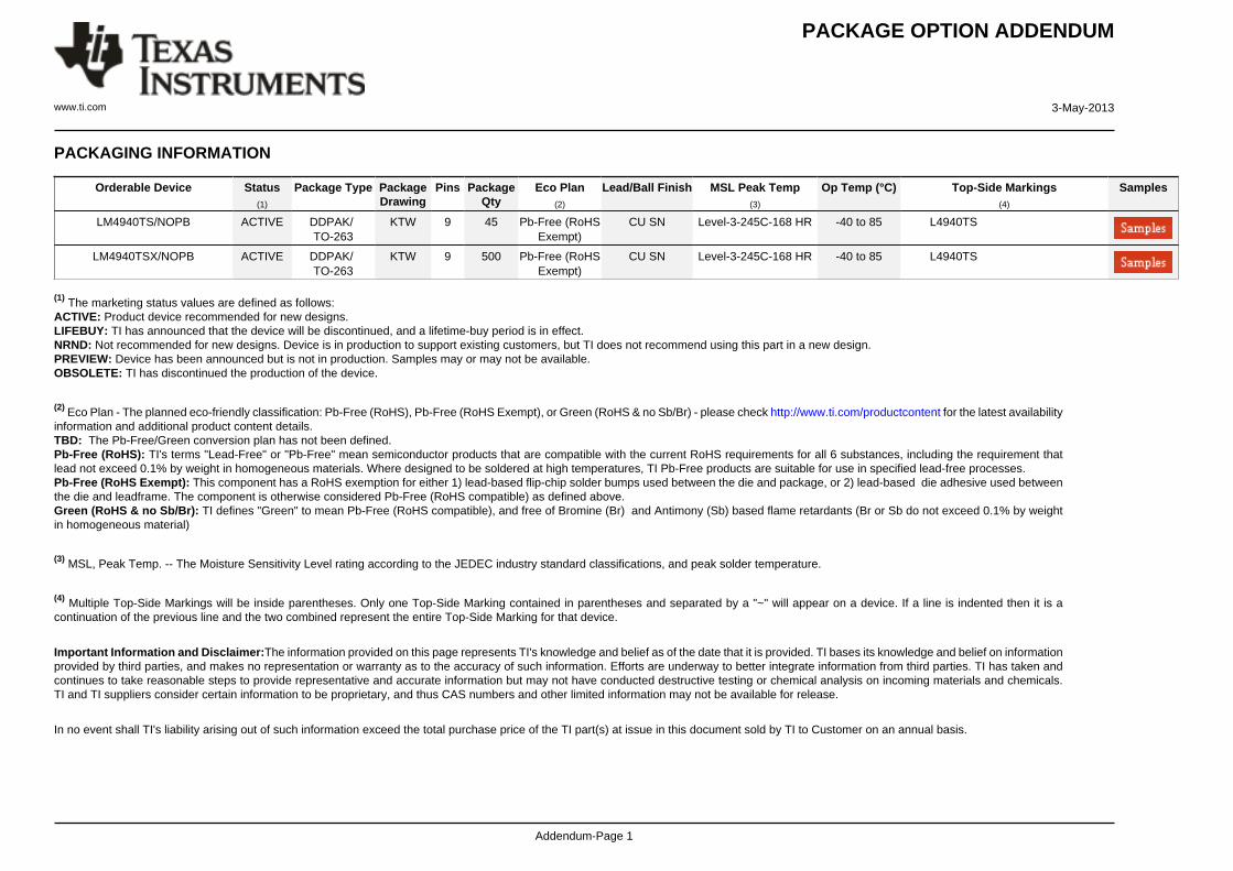
PACKAGING INFORMATION
Orderable Device Status(1)
Package Type PackageDrawing
Pins PackageQty
Eco Plan(2)
Lead/Ball Finish MSL Peak Temp(3)
Op Temp (°C) Top-Side Markings(4)
Samples
LM4940TS/NOPB ACTIVE DDPAK/TO-263
KTW 9 45 Pb-Free (RoHSExempt)
CU SN Level-3-245C-168 HR -40 to 85 L4940TS
LM4940TSX/NOPB ACTIVE DDPAK/TO-263
KTW 9 500 Pb-Free (RoHSExempt)
CU SN Level-3-245C-168 HR -40 to 85 L4940TS
(1) The marketing status values are defined as follows:ACTIVE: Product device recommended for new designs.LIFEBUY: TI has announced that the device will be discontinued, and a lifetime-buy period is in effect.NRND: Not recommended for new designs. Device is in production to support existing customers, but TI does not recommend using this part in a new design.PREVIEW: Device has been announced but is not in production. Samples may or may not be available.OBSOLETE: TI has discontinued the production of the device.
(2) Eco Plan - The planned eco-friendly classification: Pb-Free (RoHS), Pb-Free (RoHS Exempt), or Green (RoHS & no Sb/Br) - please check http://www.ti.com/productcontent for the latest availabilityinformation and additional product content details.TBD: The Pb-Free/Green conversion plan has not been defined.Pb-Free (RoHS): TI's terms "Lead-Free" or "Pb-Free" mean semiconductor products that are compatible with the current RoHS requirements for all 6 substances, including the requirement thatlead not exceed 0.1% by weight in homogeneous materials. Where designed to be soldered at high temperatures, TI Pb-Free products are suitable for use in specified lead-free processes.Pb-Free (RoHS Exempt): This component has a RoHS exemption for either 1) lead-based flip-chip solder bumps used between the die and package, or 2) lead-based die adhesive used betweenthe die and leadframe. The component is otherwise considered Pb-Free (RoHS compatible) as defined above.Green (RoHS & no Sb/Br): TI defines "Green" to mean Pb-Free (RoHS compatible), and free of Bromine (Br) and Antimony (Sb) based flame retardants (Br or Sb do not exceed 0.1% by weightin homogeneous material)
(3) MSL, Peak Temp. -- The Moisture Sensitivity Level rating according to the JEDEC industry standard classifications, and peak solder temperature.
(4) Multiple Top-Side Markings will be inside parentheses. Only one Top-Side Marking contained in parentheses and separated by a "~" will appear on a device. If a line is indented then it is acontinuation of the previous line and the two combined represent the entire Top-Side Marking for that device.
Important Information and Disclaimer:The information provided on this page represents TI's knowledge and belief as of the date that it is provided. TI bases its knowledge and belief on informationprovided by third parties, and makes no representation or warranty as to the accuracy of such information. Efforts are underway to better integrate information from third parties. TI has taken andcontinues to take reasonable steps to provide representative and accurate information but may not have conducted destructive testing or chemical analysis on incoming materials and chemicals.TI and TI suppliers consider certain information to be proprietary, and thus CAS numbers and other limited information may not be available for release.
In no event shall TI's liability arising out of such information exceed the total purchase price of the TI part(s) at issue in this document sold by TI to Customer on an annual basis.
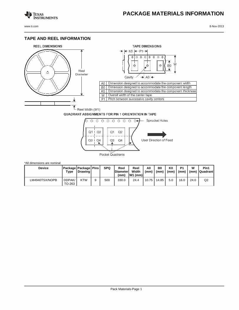
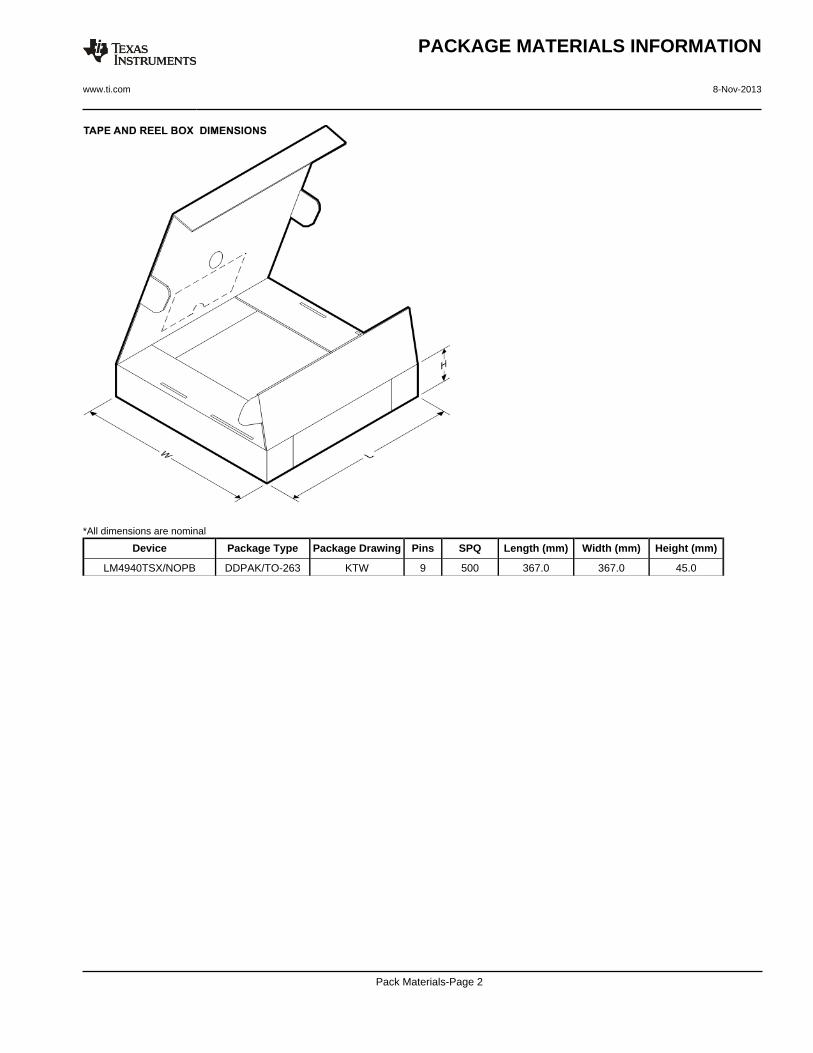
TAPE AND REEL INFORMATION
*All dimensions are nominal
Device PackageType
PackageDrawing
Pins SPQ ReelDiameter
(mm)
ReelWidth
W1 (mm)
A0(mm)
B0(mm)
K0(mm)
P1(mm)
W(mm)
Pin1Quadrant
LM4940TSX/NOPB DDPAK/TO-263
KTW 9 500 330.0 24.4 10.75 14.85 5.0 16.0 24.0 Q2
PACKAGE MATERIALS INFORMATION
www.ti.com 8-Nov-2013
Pack Materials-Page 1
*All dimensions are nominal
Device Package Type Package Drawing Pins SPQ Length (mm) Width (mm) Height (mm)
LM4940TSX/NOPB DDPAK/TO-263 KTW 9 500 367.0 367.0 45.0
PACKAGE MATERIALS INFORMATION
www.ti.com 8-Nov-2013
Pack Materials-Page 2
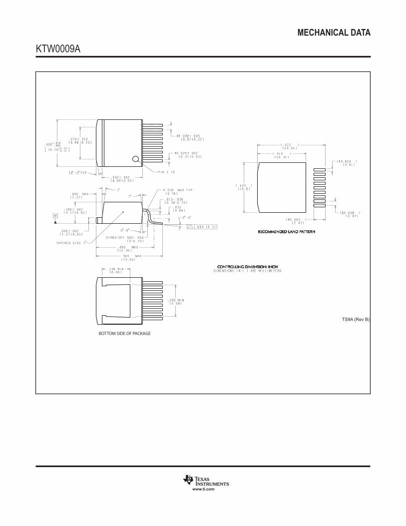
MECHANICAL DATA
KTW0009A
www.ti.com
BOTTOM SIDE OF PACKAGE
TS9A (Rev B)
IMPORTANT NOTICE
Texas Instruments Incorporated and its subsidiaries (TI) reserve the right to make corrections, enhancements, improvements and otherchanges to its semiconductor products and services per JESD46, latest issue, and to discontinue any product or service per JESD48, latestissue. Buyers should obtain the latest relevant information before placing orders and should verify that such information is current andcomplete. All semiconductor products (also referred to herein as “components”) are sold subject to TI’s terms and conditions of salesupplied at the time of order acknowledgment.
TI warrants performance of its components to the specifications applicable at the time of sale, in accordance with the warranty in TI’s termsand conditions of sale of semiconductor products. Testing and other quality control techniques are used to the extent TI deems necessaryto support this warranty. Except where mandated by applicable law, testing of all parameters of each component is not necessarilyperformed.
TI assumes no liability for applications assistance or the design of Buyers’ products. Buyers are responsible for their products andapplications using TI components. To minimize the risks associated with Buyers’ products and applications, Buyers should provideadequate design and operating safeguards.
TI does not warrant or represent that any license, either express or implied, is granted under any patent right, copyright, mask work right, orother intellectual property right relating to any combination, machine, or process in which TI components or services are used. Informationpublished by TI regarding third-party products or services does not constitute a license to use such products or services or a warranty orendorsement thereof. Use of such information may require a license from a third party under the patents or other intellectual property of thethird party, or a license from TI under the patents or other intellectual property of TI.
Reproduction of significant portions of TI information in TI data books or data sheets is permissible only if reproduction is without alterationand is accompanied by all associated warranties, conditions, limitations, and notices. TI is not responsible or liable for such altereddocumentation. Information of third parties may be subject to additional restrictions.
Resale of TI components or services with statements different from or beyond the parameters stated by TI for that component or servicevoids all express and any implied warranties for the associated TI component or service and is an unfair and deceptive business practice.TI is not responsible or liable for any such statements.
Buyer acknowledges and agrees that it is solely responsible for compliance with all legal, regulatory and safety-related requirementsconcerning its products, and any use of TI components in its applications, notwithstanding any applications-related information or supportthat may be provided by TI. Buyer represents and agrees that it has all the necessary expertise to create and implement safeguards whichanticipate dangerous consequences of failures, monitor failures and their consequences, lessen the likelihood of failures that might causeharm and take appropriate remedial actions. Buyer will fully indemnify TI and its representatives against any damages arising out of the useof any TI components in safety-critical applications.
In some cases, TI components may be promoted specifically to facilitate safety-related applications. With such components, TI’s goal is tohelp enable customers to design and create their own end-product solutions that meet applicable functional safety standards andrequirements. Nonetheless, such components are subject to these terms.
No TI components are authorized for use in FDA Class III (or similar life-critical medical equipment) unless authorized officers of the partieshave executed a special agreement specifically governing such use.
Only those TI components which TI has specifically designated as military grade or “enhanced plastic” are designed and intended for use inmilitary/aerospace applications or environments. Buyer acknowledges and agrees that any military or aerospace use of TI componentswhich have not been so designated is solely at the Buyer's risk, and that Buyer is solely responsible for compliance with all legal andregulatory requirements in connection with such use.
TI has specifically designated certain components as meeting ISO/TS16949 requirements, mainly for automotive use. In any case of use ofnon-designated products, TI will not be responsible for any failure to meet ISO/TS16949.
Products Applications
Audio www.ti.com/audio Automotive and Transportation www.ti.com/automotive
Amplifiers amplifier.ti.com Communications and Telecom www.ti.com/communications
Data Converters dataconverter.ti.com Computers and Peripherals www.ti.com/computers
DLP® Products www.dlp.com Consumer Electronics www.ti.com/consumer-apps
DSP dsp.ti.com Energy and Lighting www.ti.com/energy
Clocks and Timers www.ti.com/clocks Industrial www.ti.com/industrial
Interface interface.ti.com Medical www.ti.com/medical
Logic logic.ti.com Security www.ti.com/security
Power Mgmt power.ti.com Space, Avionics and Defense www.ti.com/space-avionics-defense
Microcontrollers microcontroller.ti.com Video and Imaging www.ti.com/video
RFID www.ti-rfid.com
OMAP Applications Processors www.ti.com/omap TI E2E Community e2e.ti.com
Wireless Connectivity www.ti.com/wirelessconnectivity
Mailing Address: Texas Instruments, Post Office Box 655303, Dallas, Texas 75265Copyright © 2013, Texas Instruments Incorporated