Embed Size (px)
Citation preview
LM5072
www.ti.com SNVS437D –MARCH 2006–REVISED APRIL 2013
LM5072 Integrated 100V Power Over Ethernet PD Interface and PWM Controller with AuxSupport
Check for Samples: LM5072
1FEATURES DESCRIPTIONThe LM5072 Powered Device (PD) interface and
2• PD InterfacePulse-Width-Modulation (PWM) controller provides a
– Fully Compliant IEEE 802.3af PD Interface complete power solution, fully compliant to IEEE– Versatile Auxiliary Power Options 802.3af, for the PD connecting into Power over
Ethernet (PoE) networks. This controller integrates all– 9V Minimum Auxiliary Power Operatingfunctions necessary to implement both a PD poweredRangeinterface and DC-DC converter with a minimum
– 100V Maximum Input Voltage Rating number of external components. The LM5072– Programmable DC Current Limit Up To provides the flexibility for the PD to also accept power
800mA from auxiliary sources such as AC adapters in avariety of configurations. The low RDS(ON) PD– 100V, 0.7Ω Hot Swap MOSFETinterface hot swap MOSFET and programmable DC
– Integrated PD Signature Resistor current limit extend the range of LM5072 applications– Integrated PoE Input UVLO up to twice the power level of 802.3af compliant PD
devices. The 100V maximum voltage rating simplifies– Programmable Inrush Current Limitselection of the transient voltage suppressor that– PD Classification Capability protects the PD from network transients. The LM5072
– Power Good Indicator includes an easy-to-use PWM controller thatfacilitates the various single-ended power supply– Thermal Shutdown Protectiontopologies including the flyback, forward and buck.• PWM ControllerThe PWM control scheme is based on peak current
– Current Mode PWM Controller mode control, which provides inherent advantagesincluding line feed-forward, cycle-by-cycle current– 100V Start-Up Regulatorlimit, and simplified feedback loop compensation.– Error Amplifier with 2% Voltage ReferenceTwo versions of the LM5072 provide either an 80%
– Supports Isolated and Non-Isolated maximum duty cycle (-80 suffix), or a 50% maximumApplications duty cycle (-50 suffix).
– Programmable Oscillator FrequencyPACKAGES– Programmable Soft-Start• TSSOP-16 EP (Exposed Pad)– 800 mA Peak Gate Driver
– 80% Maximum Duty Cycle with Built-inSlope Compensation (-80 Device)
– 50% Maximum Duty Cycle, No SlopeCompensation (-50 Device)
APPLICATIONS• IEEE 802.3af Compliant PoE Powered Devices• Non-Compliant, Application Specific Devices• Higher Power Ethernet Powered Devices
1
Please be aware that an important notice concerning availability, standard warranty, and use in critical applications ofTexas Instruments semiconductor products and disclaimers thereto appears at the end of this data sheet.
2All trademarks are the property of their respective owners.
PRODUCTION DATA information is current as of publication date. Copyright © 2006–2013, Texas Instruments IncorporatedProducts conform to specifications per the terms of the TexasInstruments standard warranty. Production processing does notnecessarily include testing of all parameters.
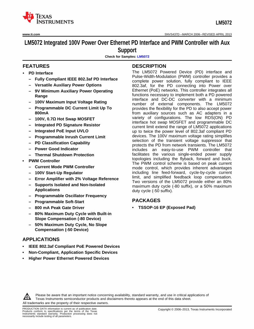
VIN
RCLASS
VEE VCC
OUT
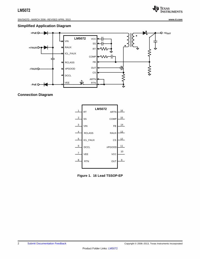
RT
FB
CS
COMP
RAUX
SS
RTN
ARTN
nPGOOD
LM5072
ICL_FAUX
DCCL
1
2
3
4
5
6
7
8
16
15
14
13
12
11
10
9
VIN
RAUX
VEE
OUT
RT
CS
FB
COMP
SS
RTN
ARTN
DCCL
RCLASS
nPGOOD
VCC
+PoE
+ FAUX
- FAUX
-PoE
LM5072
+VOUT
ICL_FAUX
LM5072
SNVS437D –MARCH 2006–REVISED APRIL 2013 www.ti.com
Simplified Application Diagram
Connection Diagram
Figure 1. 16 Lead TSSOP-EP
2 Submit Documentation Feedback Copyright © 2006–2013, Texas Instruments Incorporated
Product Folder Links: LM5072
LM5072
www.ti.com SNVS437D –MARCH 2006–REVISED APRIL 2013
PIN DESCRIPTIONSPin Number Name Description
1 RT PWM controller oscillator frequency programming pin.
2 SS Soft-start programming pin.
3 VIN Positive supply pin for the PD interface and the internal PWM controller start-up regulator.
4 RCLASS PD classification programming pin.
5 ICL_FAUX Inrush current limit programming pin; also the front auxiliary power enable pin.
6 DCCL PD interface DC current limit programming pin.
7 VEE Negative supply pin for PD interface; connected to PoE and/or front auxiliary power return path.
8 RTN PWM controller power return; connected to the drain of the internal PD interface hot swapMOSFET; should be externally connected to the reference ground of the PWM controller.
9 OUT PWM controller gate driver output pin.
10 VCC PWM controller start-up regulator output pin.
11 nPGOOD PD interface Power Good indicator and delay timer pin; active low state indicates PoE interface is innormal operation.
12 CS PWM controller current sense input pin.
13 RAUX Rear auxiliary power enable pin; can be programmed for auxiliary power dominance over PoEpower.
14 FB PWM controller voltage feedback pin and inverting input of the internal error amplifier; connect toARTN to disable the error amplifier in isolated dc-dc converter applications.
15 COMP Output of the internal error amplifier and control input to the PWM comparator. In isolatedapplications, COMP is controlled by the secondary side error amplifier via an opto-coupler.
16 ARTN PWM controller reference ground pin; should be shorted externally to the RTN pin as a single pointground connection to improve noise immunity.
EP Exposed metal pad on the underside of the device. It is recommended to connect this pad to a PCBoard plane connected to the VEE pin to improve heat dissipation.
These devices have limited built-in ESD protection. The leads should be shorted together or the device placed in conductive foamduring storage or handling to prevent electrostatic damage to the MOS gates.
Copyright © 2006–2013, Texas Instruments Incorporated Submit Documentation Feedback 3
Product Folder Links: LM5072
LM5072
SNVS437D –MARCH 2006–REVISED APRIL 2013 www.ti.com
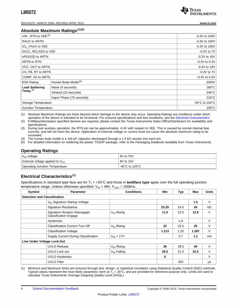
Absolute Maximum Ratings (1) (2)
VIN , RTN to VEE (3) -0.3V to 100V
RAUX to ARTN -0.3V to 100V
ICL_FAUX to VEE -0.3V to 100V
DCCL, RCLASS to VEE -0.3V to 7V
nPGOOD to ARTN -0.3V to 16V
ARTN to RTN -0.3V to 0.3V
VCC, OUT to ARTN -0.3V to 16V
CS, FB, RT to ARTN -0.3V to 7V
COMP, SS to ARTN -0.3V to 5.5V
ESD Rating Human Body Model (4) 2000V
Lead Soldering Wave (4 seconds) 260°CTemp. (5)
Infrared (10 seconds) 240°C
Vapor Phase (75 seconds) 219°C
Storage Temperature -55°C to 150°C
Junction Temperature 150°C
(1) Absolute Maximum Ratings are limits beyond which damage to the device may occur. Operating Ratings are conditions under whichoperation of the device is intended to be functional. For ensured specifications and test conditions, see the Electrical Characteristics
(2) If Military/Aerospace specified devices are required, please contact the Texas Instruments Sales Office/Distributors for availability andspecifications.
(3) During rear auxiliary operation, the RTN pin can be approximately -0.4V with respect to VEE. This is caused by normal internal biascurrents, and will not harm the device. Application of external voltage or current must not cause the absolute maximum rating to beexceeded.
(4) The human body model is a 100 pF capacitor discharged through a 1.5 kΩ resistor into each pin.(5) For detailed information on soldering the plastic TSSOP package, refer to the Packaging Databook available from Texas Instruments.
Operating RatingsVIN voltage 9V to 70V
External voltage applied to VCC 8V to 15V
Operating Junction Temperature -40°C to 125°C
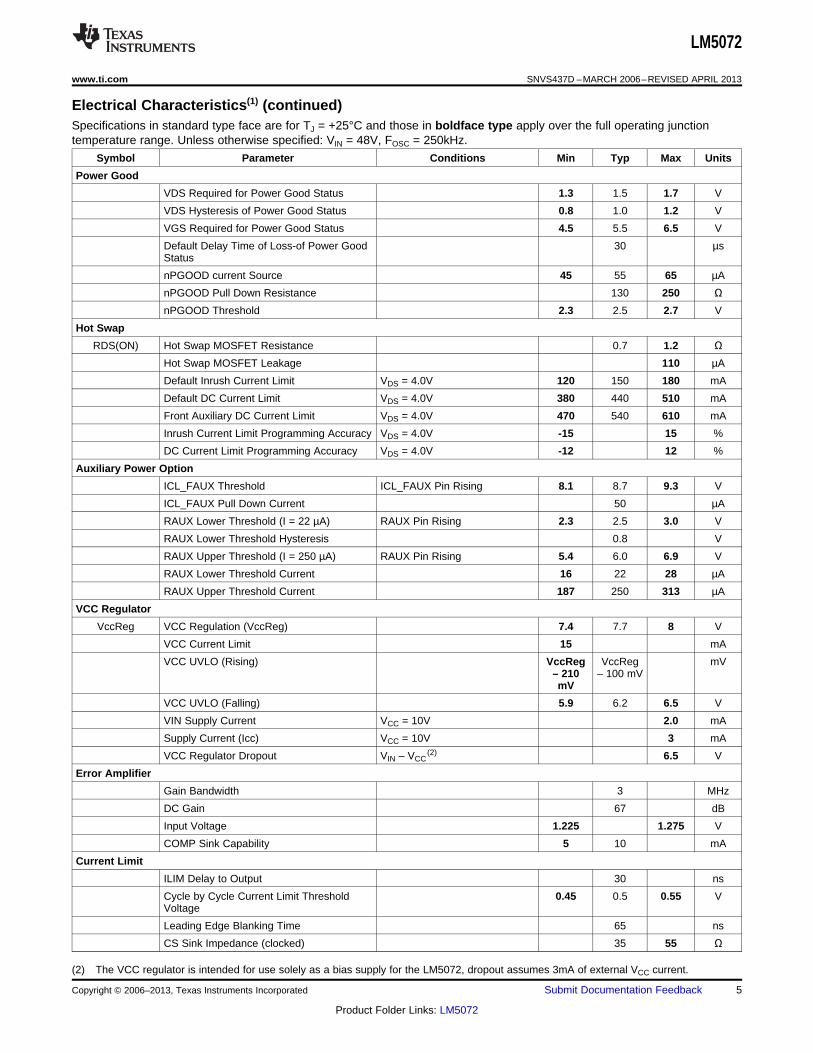
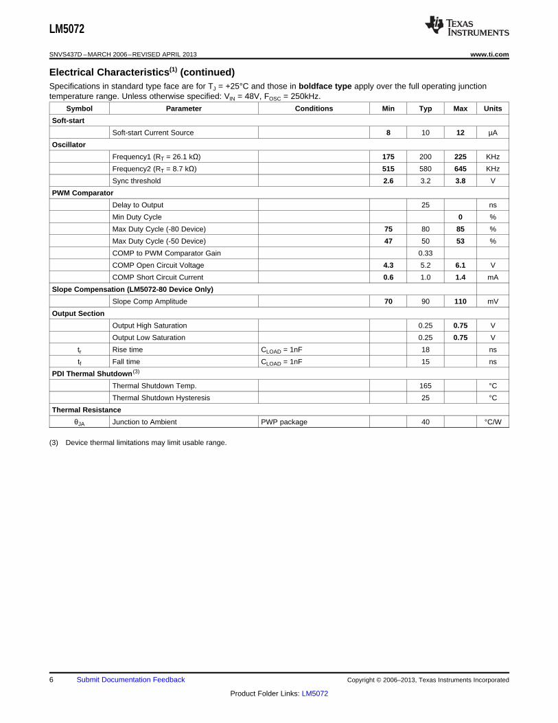
Electrical Characteristics (1)
Specifications in standard type face are for TJ = +25°C and those in boldface type apply over the full operating junctiontemperature range. Unless otherwise specified: VIN = 48V, FOSC = 250kHz.
Symbol Parameter Conditions Min Typ Max Units
Detection and Classification
VIN Signature Startup Voltage 1.5 V
Signature Resistance 23.25 24.5 26 kΩSignature Resistor Disengage/ VIN Rising 11.0 12.0 12.6 VClassification Engage
Hysteresis 1.9 V
Classification Current Turn Off VIN Rising 22 23.5 25 V
Classification Voltage 1.213 1.25 1.287 V
Supply Current During Classification VIN = 17V 0.7 1.1 mA
Line Under Voltage Lock-Out
UVLO Release VIN Rising 36 38.5 40 V
UVLO Lock out VIN Falling 29.5 31.0 32.5 V
UVLO Hysteresis 6 V
UVLO Filter 300 µs
(1) Minimum and Maximum limits are ensured through test, design, or statistical correlation using Statistical Quality Control (SQC) methods.Typical values represent the most likely parametric norm at TJ = 25°C, and are provided for reference purpose only. Limits are used tocalculate Texas Instruments' Average Outgoing Quality Level (AOQL).
4 Submit Documentation Feedback Copyright © 2006–2013, Texas Instruments Incorporated
Product Folder Links: LM5072
LM5072
www.ti.com SNVS437D –MARCH 2006–REVISED APRIL 2013
Electrical Characteristics(1) (continued)Specifications in standard type face are for TJ = +25°C and those in boldface type apply over the full operating junctiontemperature range. Unless otherwise specified: VIN = 48V, FOSC = 250kHz.
Symbol Parameter Conditions Min Typ Max Units
Power Good
VDS Required for Power Good Status 1.3 1.5 1.7 V
VDS Hysteresis of Power Good Status 0.8 1.0 1.2 V
VGS Required for Power Good Status 4.5 5.5 6.5 V
Default Delay Time of Loss-of Power Good 30 µsStatus
nPGOOD current Source 45 55 65 µA
nPGOOD Pull Down Resistance 130 250 ΩnPGOOD Threshold 2.3 2.5 2.7 V
Hot Swap
RDS(ON) Hot Swap MOSFET Resistance 0.7 1.2 ΩHot Swap MOSFET Leakage 110 µA
Default Inrush Current Limit VDS = 4.0V 120 150 180 mA
Default DC Current Limit VDS = 4.0V 380 440 510 mA
Front Auxiliary DC Current Limit VDS = 4.0V 470 540 610 mA
Inrush Current Limit Programming Accuracy VDS = 4.0V -15 15 %
DC Current Limit Programming Accuracy VDS = 4.0V -12 12 %
Auxiliary Power Option
ICL_FAUX Threshold ICL_FAUX Pin Rising 8.1 8.7 9.3 V
ICL_FAUX Pull Down Current 50 µA
RAUX Lower Threshold (I = 22 µA) RAUX Pin Rising 2.3 2.5 3.0 V
RAUX Lower Threshold Hysteresis 0.8 V
RAUX Upper Threshold (I = 250 µA) RAUX Pin Rising 5.4 6.0 6.9 V
RAUX Lower Threshold Current 16 22 28 µA
RAUX Upper Threshold Current 187 250 313 µA
VCC Regulator
VccReg VCC Regulation (VccReg) 7.4 7.7 8 V
VCC Current Limit 15 mA
VCC UVLO (Rising) VccReg VccReg mV– 210 – 100 mVmV
VCC UVLO (Falling) 5.9 6.2 6.5 V
VIN Supply Current VCC = 10V 2.0 mA
Supply Current (Icc) VCC = 10V 3 mA
VCC Regulator Dropout VIN – VCC(2) 6.5 V
Error Amplifier
Gain Bandwidth 3 MHz
DC Gain 67 dB
Input Voltage 1.225 1.275 V
COMP Sink Capability 5 10 mA
Current Limit
ILIM Delay to Output 30 ns
Cycle by Cycle Current Limit Threshold 0.45 0.5 0.55 VVoltage
Leading Edge Blanking Time 65 ns
CS Sink Impedance (clocked) 35 55 Ω
(2) The VCC regulator is intended for use solely as a bias supply for the LM5072, dropout assumes 3mA of external VCC current.
Copyright © 2006–2013, Texas Instruments Incorporated Submit Documentation Feedback 5
Product Folder Links: LM5072
LM5072
SNVS437D –MARCH 2006–REVISED APRIL 2013 www.ti.com
Electrical Characteristics(1) (continued)Specifications in standard type face are for TJ = +25°C and those in boldface type apply over the full operating junctiontemperature range. Unless otherwise specified: VIN = 48V, FOSC = 250kHz.
Symbol Parameter Conditions Min Typ Max Units
Soft-start
Soft-start Current Source 8 10 12 µA
Oscillator
Frequency1 (RT = 26.1 kΩ) 175 200 225 KHz
Frequency2 (RT = 8.7 kΩ) 515 580 645 KHz
Sync threshold 2.6 3.2 3.8 V
PWM Comparator
Delay to Output 25 ns
Min Duty Cycle 0 %
Max Duty Cycle (-80 Device) 75 80 85 %
Max Duty Cycle (-50 Device) 47 50 53 %
COMP to PWM Comparator Gain 0.33
COMP Open Circuit Voltage 4.3 5.2 6.1 V
COMP Short Circuit Current 0.6 1.0 1.4 mA
Slope Compensation (LM5072-80 Device Only)
Slope Comp Amplitude 70 90 110 mV
Output Section
Output High Saturation 0.25 0.75 V
Output Low Saturation 0.25 0.75 V
tr Rise time CLOAD = 1nF 18 ns
tf Fall time CLOAD = 1nF 15 ns
PDI Thermal Shutdown (3)
Thermal Shutdown Temp. 165 °C
Thermal Shutdown Hysteresis 25 °C
Thermal Resistance
θJA Junction to Ambient PWP package 40 °C/W
(3) Device thermal limitations may limit usable range.
6 Submit Documentation Feedback Copyright © 2006–2013, Texas Instruments Incorporated
Product Folder Links: LM5072
-40 -20 0 20 40 60 80 100 120
TEMPERATURE (ºC)
PR
OG
RA
MM
ED
DC
CU
RR
EN
T L
IMIT
(m
A)
350
355
360
365
370
375
380
385
390
395
400
-40 -20 0 20 40 60 80 100 120
TEMPERATURE (ºC)
OS
CIL
LAT
OR
FR
EQ
UE
NC
Y (
kHz)
250
252
254
256
258
260
262
264
CU
RR
EN
T L
IMIT
(m
A)
15 25 35 45 55 65 75 85 115
PROGRAMMING RESISTANCE (k:)
95 105100
200
300
400
500
600
700
800
CU
RR
EN
T L
IMIT
(m
A)
15 25 35 45 55 65 75 85 115
PROGRAMMING RESISTANCE (k:)
95 105100
200
300
400
500
600
700
800
UV
LO T
HR
ES
HO
LD (
V)
30.0
30.5
31.0
31.5
32.0
-40 -20 0 20 40 60 80 100 120
TEMPERATURE (ºC)
DC
CU
RR
EN
T L
IMIT
(m
A)
-40 -20 0 20 40 60 80 100 120
TEMPERATURE (ºC)
425
430
435
440
445
450
455
460
465
470
475
LM5072
www.ti.com SNVS437D –MARCH 2006–REVISED APRIL 2013
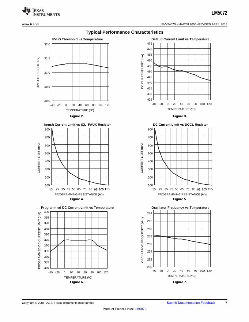
Typical Performance Characteristics
UVLO Threshold vs Temperature Default Current Limit vs Temperature
Figure 2. Figure 3.
Inrush Current Limit vs ICL_FAUX Resistor DC Current Limit vs DCCL Resistor
Figure 4. Figure 5.
Programmed DC Current Limit vs Temperature Oscillator Frequency vs Temperature
Figure 6. Figure 7.
Copyright © 2006–2013, Texas Instruments Incorporated Submit Documentation Feedback 7
Product Folder Links: LM5072
-40 -20 0 20 40 60 80 100 120
TEMPERATURE (ºC)
MA
X D
UT
Y C
YC
LE (
%)
78
79
80
81
82
83
84
SO
FT
ST
AR
T C
UR
RE
NT
(P
A)
-40 -20 0 20 40 60 80 100 120
TEMPERATURE (ºC)
10.0
10.1
10.2
10.3
10.4
10.5
ICC (mA)
VC
C (
V)
0
1
2
3
4
5
6
7
8
9
0 5 10 15 20
VCC
0 10 20 30 40 50 60
VIN (V)
I IN (
mA
)
0.00E+00
5.00E-01
1.00E+00
1.50E+00
2.00E+00
2.50E+00
3.00E+00
5 15 25 35 45 55 65 75 85 95 1050
100
200
300
400
500
600
700
800
900
1000O
SC
ILLA
TO
R F
RE
QU
EN
CY
(kH
z)
RT RESISTANCE (k:)
E/A
RE
FE
RE
NC
E V
OLT
AG
E (
V)
-40 -20 0 20 40 60 80 100 120
TEMPERATURE (ºC)
1.2250
1.2350
1.2450
1.2550
1.2650
1.2750
LM5072
SNVS437D –MARCH 2006–REVISED APRIL 2013 www.ti.com
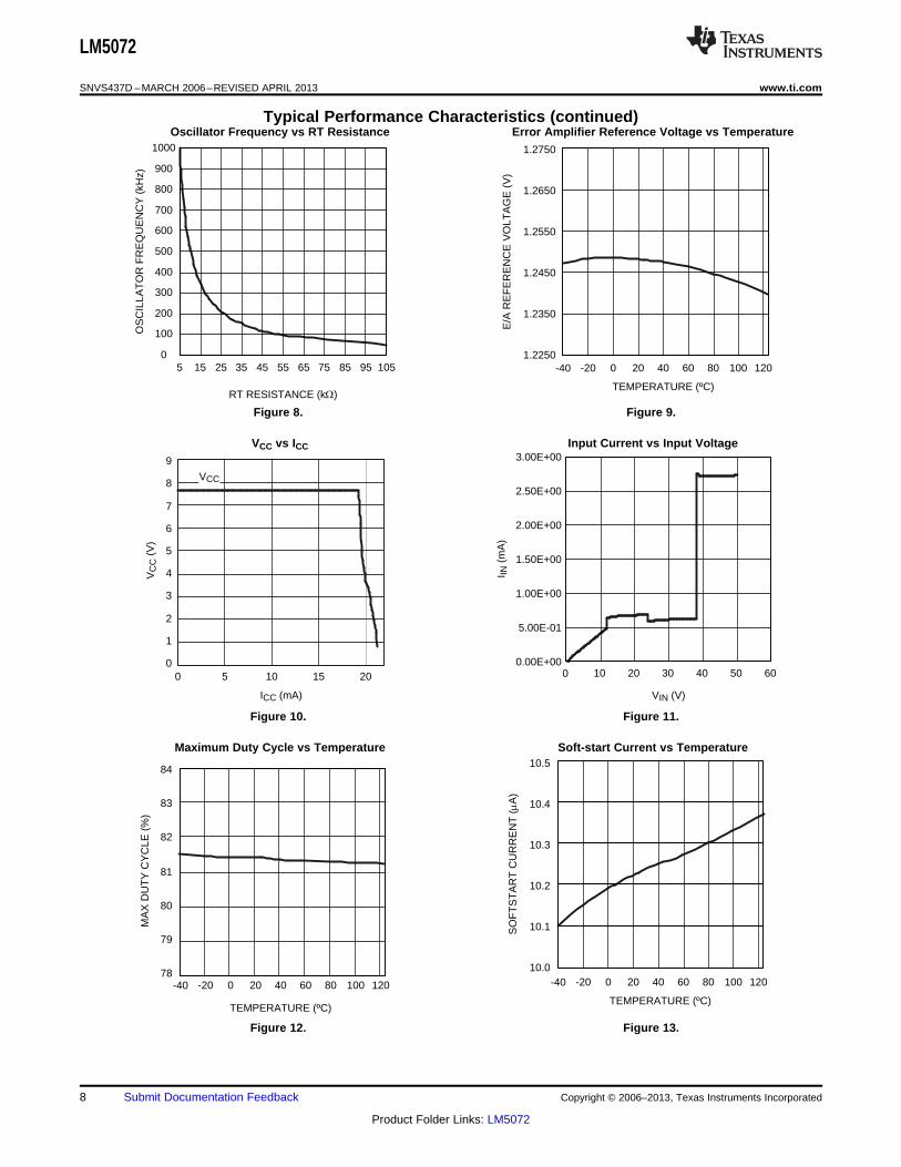
Typical Performance Characteristics (continued)Oscillator Frequency vs RT Resistance Error Amplifier Reference Voltage vs Temperature
Figure 8. Figure 9.
VCC vs ICC Input Current vs Input Voltage
Figure 10. Figure 11.
Maximum Duty Cycle vs Temperature Soft-start Current vs Temperature
Figure 12. Figure 13.
8 Submit Documentation Feedback Copyright © 2006–2013, Texas Instruments Incorporated
Product Folder Links: LM5072
3VIN
7VEE
4RCLASS
8 RTN
PWM Controller
2 SS
16 ARTN
9 OUT
10 VCC
GateController
EN
+
-
+
-
+
-
+
-
5
+
-
+
-
6DCCL
+
-
UVLO
+ - +-
S R
Q
+
-
1 RT
12 CS
15 COMP
14 FB
+
-
11 nPGOOD
13 RAUX
+
-
AuxiliaryController
signature
VCC
Hot Swap MOSFET
EN
5V
1.5V
ICL_FAUX
24.5 k:
50 PA
50 PA
po
dg
o
.2 5V
V2.42.0V
1 25. V
1 25. V
thermal_limit
1 25. V
1 25. V
1 .02 V
.2 5V
.25V
Threshold VIN = 25V
Threshold VIN= 38VVIN Hysteresis= 6V
1 25. V
front_aux
Dis
able
5V_PDI
Disable_PDI
LM5072
www.ti.com SNVS437D –MARCH 2006–REVISED APRIL 2013
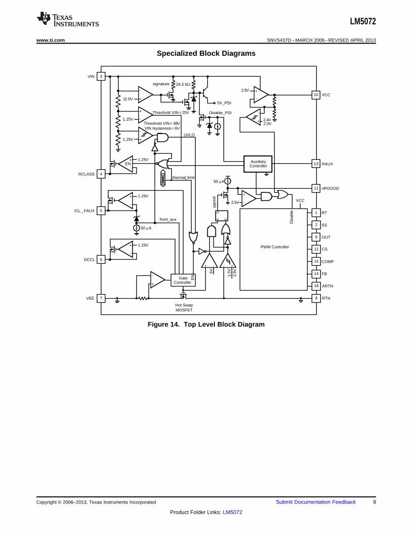
Specialized Block Diagrams
Figure 14. Top Level Block Diagram
Copyright © 2006–2013, Texas Instruments Incorporated Submit Documentation Feedback 9
Product Folder Links: LM5072
CS
LOGIC
OUT
DRIVER
PWM
SS to Error Amplifier
CLK
SS
(
Q
QSET
S
R
CURRENTLIMIT
OSC RT
1
FB
SlopeCompensation
Generator0
SS
ARTN
COMP
current sense 16
12
9
2
15
1450k
100k
1.4V
5k
V1.25
2k
0.5V
5V
45PA
Slope Compensation
disabled for -50 Device
10 PA
CLR
CLK + LEB
65 ns blanking
50 % MAX
80% MAX
-DUTY LIMIT ( 50)
- )DUTY LIMIT 80
LM5072
SNVS437D –MARCH 2006–REVISED APRIL 2013 www.ti.com
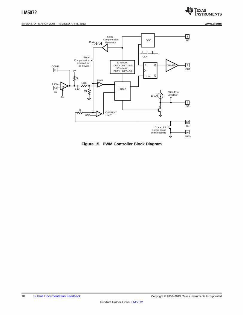
Figure 15. PWM Controller Block Diagram
10 Submit Documentation Feedback Copyright © 2006–2013, Texas Instruments Incorporated
Product Folder Links: LM5072
LM5072
www.ti.com SNVS437D –MARCH 2006–REVISED APRIL 2013
DESCRIPTION OF OPERATION AND APPLICATIONS INFORMATION
The LM5072 integrates a fully IEEE 802.3af compliant PD interface and PWM controller in a single integratedcircuit, providing a complete and low cost power solution for devices that connect to PoE systems. Theimplementation requires a minimal number of external components.
The LM5072’s Hot Swap PD interface provides four major advantages:1. An input voltage rating up to 100V that allows greater flexibility when selecting a transient surge suppressor
to protect the PD from voltage transients encountered in PoE applications.2. The integration of the PD signature resistor and other functions including programmable inrush current limit,
input voltage under-voltage lock-out (UVLO), PD classification, and thermal shutdown simplifies PDimplementation.
3. The PD interface and PWM controller accept power from auxiliary sources including AC adapters and solarcells in various configurations and over a wide range of input voltages. Auxiliary power input can beprogrammed to be dominant over PoE power.
4. DC current limit is programmable and adjustable to support PoE applications requiring input currents up to700 mA.
The LM5072 includes an easy to use PWM controller based on the peak current mode control technique. Currentmode control provides inherent advantages such as line voltage feed-forward, cycle-by-cycle current limit, andsimplified closed-loop compensation. The controller’s PWM gate driver is capable of sourcing and sinking peakcurrents of 800 mA to directly drive the power MOSFET switch of the DC-DC converter. The PWM controller alsocontains a high gain, high bandwidth error amplifier, a high voltage startup bias regulator, a programmableoscillator for a switching frequency between 50 kHz to 500 kHz, a bias supply (VCC) under-voltage lock-outcircuit, and a programmable soft-start circuit. These features greatly simplify the design and implementation ofsingle ended topologies like the flyback, forward and buck.
The LM5072 is available in two versions, the LM5072-50 and LM5072-80. As indicated in the suffix of the partnumber, the maximum duty cycle of each device is limited to 50% and 80%, respectively. Internal PWM controllerslope compensation is provided in the LM5072-80 version.
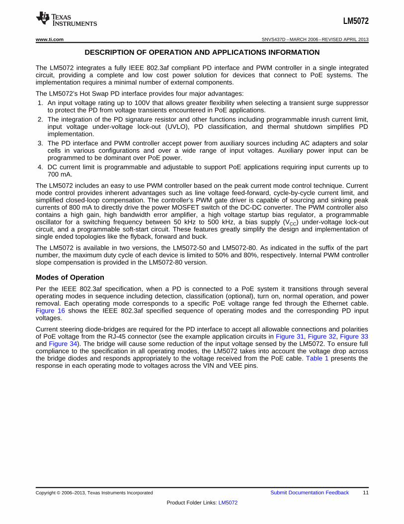
Modes of Operation
Per the IEEE 802.3af specification, when a PD is connected to a PoE system it transitions through severaloperating modes in sequence including detection, classification (optional), turn on, normal operation, and powerremoval. Each operating mode corresponds to a specific PoE voltage range fed through the Ethernet cable.Figure 16 shows the IEEE 802.3af specified sequence of operating modes and the corresponding PD inputvoltages.
Current steering diode-bridges are required for the PD interface to accept all allowable connections and polaritiesof PoE voltage from the RJ-45 connector (see the example application circuits in Figure 31, Figure 32, Figure 33and Figure 34). The bridge will cause some reduction of the input voltage sensed by the LM5072. To ensure fullcompliance to the specification in all operating modes, the LM5072 takes into account the voltage drop acrossthe bridge diodes and responds appropriately to the voltage received from the PoE cable. Table 1 presents theresponse in each operating mode to voltages across the VIN and VEE pins.
Copyright © 2006–2013, Texas Instruments Incorporated Submit Documentation Feedback 11
Product Folder Links: LM5072
VEE
+
-
12V
LM5072
3
7
VIN
24.5k
PoE LineInput
PoE LineReturn
2.7V
10V
14.5V
Voltage
Discovery Classification
Classification
Time
42V
30V
Full Power Application Power Removal
LM5072
SNVS437D –MARCH 2006–REVISED APRIL 2013 www.ti.com
Figure 16. Sequence of PoE Operating Modes
Table 1. Operating Modes With Respect To Input Voltage
Mode of Operation Voltage from PoE Cable per LM5072 Input VoltageIEEE 802.3af (VIN pin to VEE pin)
Detection (Signature) 2.7V to 10.0V 1.5V to 10.0V
Classification 14.5V to 20.5V 12V to 23.5V
Startup 42V max 38V (UVLO Release, VIN Rising)
Normal Operation 57V to 36V 70V to 32V (UVLO, VIN Falling)
Detection Signature
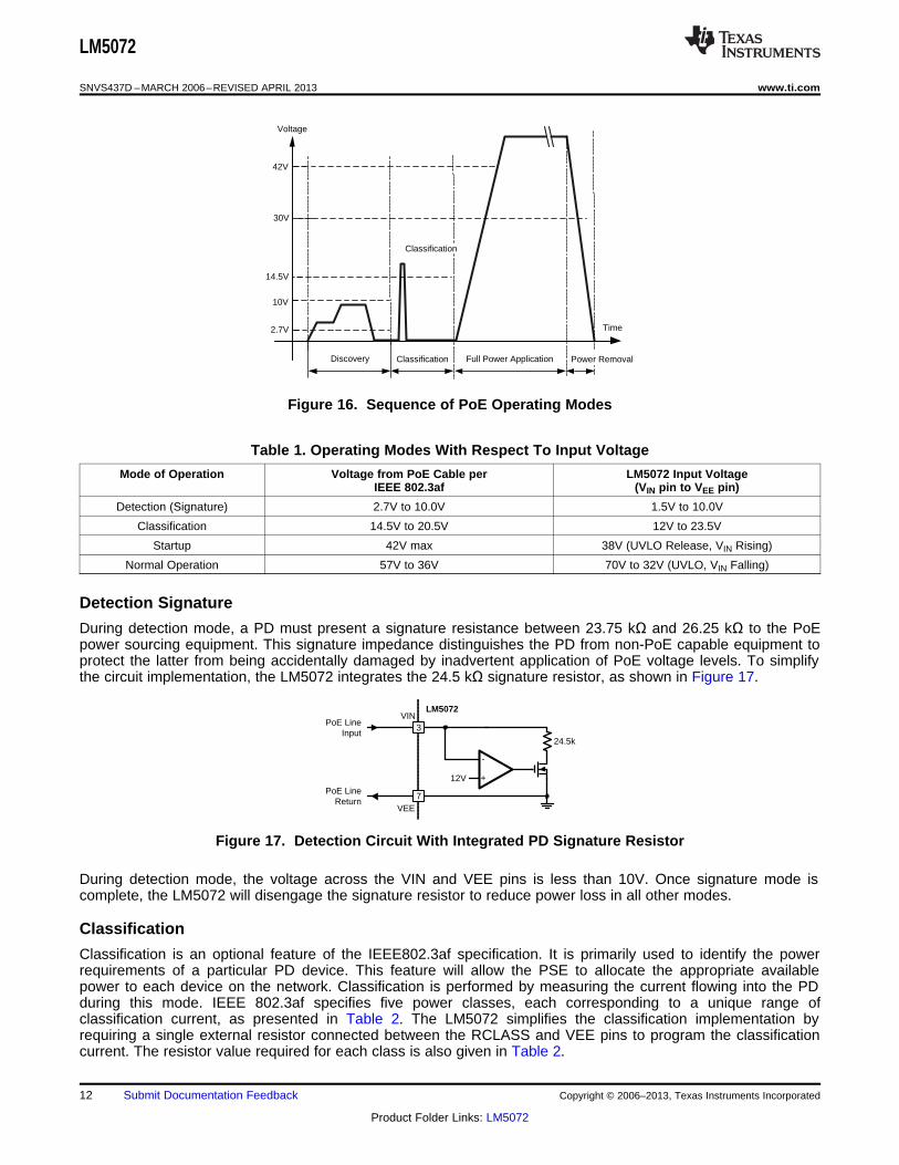
During detection mode, a PD must present a signature resistance between 23.75 kΩ and 26.25 kΩ to the PoEpower sourcing equipment. This signature impedance distinguishes the PD from non-PoE capable equipment toprotect the latter from being accidentally damaged by inadvertent application of PoE voltage levels. To simplifythe circuit implementation, the LM5072 integrates the 24.5 kΩ signature resistor, as shown in Figure 17.
Figure 17. Detection Circuit With Integrated PD Signature Resistor
During detection mode, the voltage across the VIN and VEE pins is less than 10V. Once signature mode iscomplete, the LM5072 will disengage the signature resistor to reduce power loss in all other modes.
Classification
Classification is an optional feature of the IEEE802.3af specification. It is primarily used to identify the powerrequirements of a particular PD device. This feature will allow the PSE to allocate the appropriate availablepower to each device on the network. Classification is performed by measuring the current flowing into the PDduring this mode. IEEE 802.3af specifies five power classes, each corresponding to a unique range ofclassification current, as presented in Table 2. The LM5072 simplifies the classification implementation byrequiring a single external resistor connected between the RCLASS and VEE pins to program the classificationcurrent. The resistor value required for each class is also given in Table 2.
12 Submit Documentation Feedback Copyright © 2006–2013, Texas Instruments Incorporated
Product Folder Links: LM5072
3VIN
4RCLASS
EN+
-
7
+
-
Threshold
VEE
to UVLO
PoE Line Input
PoE Line Return
VIN = 23.5V
LM5072
RCLASS
1.25V
1.25V
front_aux
rear_aux
thermal_limit
LM5072
www.ti.com SNVS437D –MARCH 2006–REVISED APRIL 2013
Table 2. Classification Levels and Required External Resistor Value
Class PD Max Power Level ICLASS Range LM5072RCLASS ValueFrom To From To
0 (Default) 0.44W 12.95W 0 mA 4 mA Open
1 0.44W 3.84W 9 mA 12 mA 130Ω2 3.84W 6.49W 17 mA 20 mA 71.5Ω3 6.49W 12.95W 26 mA 30 mA 46.4Ω4 Reserved Reserved 36 mA 44 mA 31.6Ω
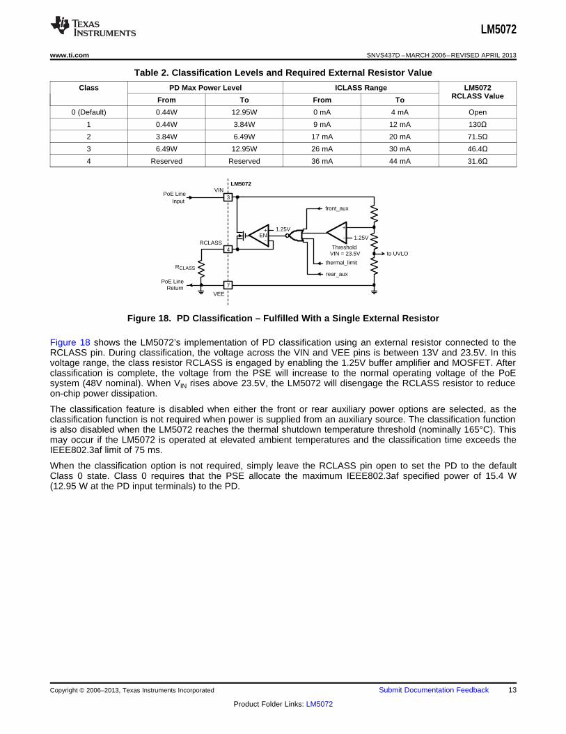
Figure 18. PD Classification – Fulfilled With a Single External Resistor
Figure 18 shows the LM5072’s implementation of PD classification using an external resistor connected to theRCLASS pin. During classification, the voltage across the VIN and VEE pins is between 13V and 23.5V. In thisvoltage range, the class resistor RCLASS is engaged by enabling the 1.25V buffer amplifier and MOSFET. Afterclassification is complete, the voltage from the PSE will increase to the normal operating voltage of the PoEsystem (48V nominal). When VIN rises above 23.5V, the LM5072 will disengage the RCLASS resistor to reduceon-chip power dissipation.
The classification feature is disabled when either the front or rear auxiliary power options are selected, as theclassification function is not required when power is supplied from an auxiliary source. The classification functionis also disabled when the LM5072 reaches the thermal shutdown temperature threshold (nominally 165°C). Thismay occur if the LM5072 is operated at elevated ambient temperatures and the classification time exceeds theIEEE802.3af limit of 75 ms.
When the classification option is not required, simply leave the RCLASS pin open to set the PD to the defaultClass 0 state. Class 0 requires that the PSE allocate the maximum IEEE802.3af specified power of 15.4 W(12.95 W at the PD input terminals) to the PD.
Copyright © 2006–2013, Texas Instruments Incorporated Submit Documentation Feedback 13
Product Folder Links: LM5072
VIN
7
VEE
GateController
To Signatureand Startup Regulator
+
-UVLO
VIN Threshold =38VHysteresis = 7V
To Classification
PoE Line Input
PoE Line Return
3
1.25V
LM5072
Converter Return
To DC/DC
Hot Swap MOSFET
front_aux
thermal_limit
EN
LM5072
SNVS437D –MARCH 2006–REVISED APRIL 2013 www.ti.com
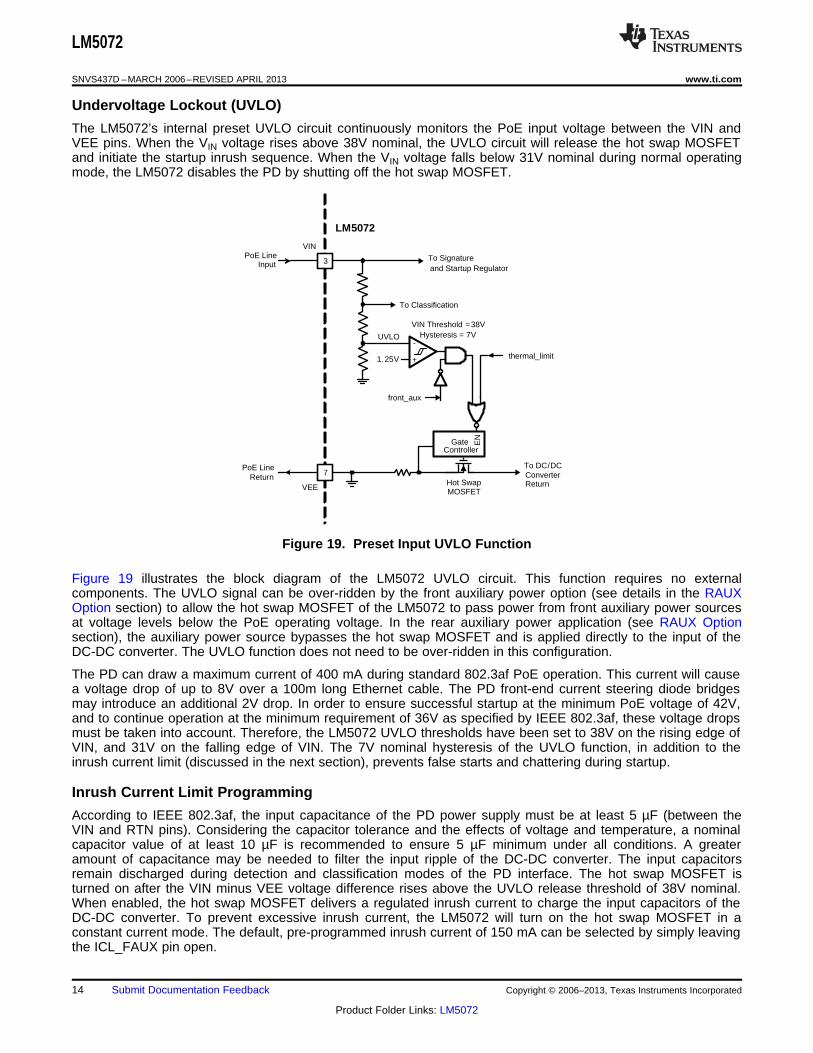
Undervoltage Lockout (UVLO)
The LM5072’s internal preset UVLO circuit continuously monitors the PoE input voltage between the VIN andVEE pins. When the VIN voltage rises above 38V nominal, the UVLO circuit will release the hot swap MOSFETand initiate the startup inrush sequence. When the VIN voltage falls below 31V nominal during normal operatingmode, the LM5072 disables the PD by shutting off the hot swap MOSFET.
Figure 19. Preset Input UVLO Function
Figure 19 illustrates the block diagram of the LM5072 UVLO circuit. This function requires no externalcomponents. The UVLO signal can be over-ridden by the front auxiliary power option (see details in the RAUXOption section) to allow the hot swap MOSFET of the LM5072 to pass power from front auxiliary power sourcesat voltage levels below the PoE operating voltage. In the rear auxiliary power application (see RAUX Optionsection), the auxiliary power source bypasses the hot swap MOSFET and is applied directly to the input of theDC-DC converter. The UVLO function does not need to be over-ridden in this configuration.
The PD can draw a maximum current of 400 mA during standard 802.3af PoE operation. This current will causea voltage drop of up to 8V over a 100m long Ethernet cable. The PD front-end current steering diode bridgesmay introduce an additional 2V drop. In order to ensure successful startup at the minimum PoE voltage of 42V,and to continue operation at the minimum requirement of 36V as specified by IEEE 802.3af, these voltage dropsmust be taken into account. Therefore, the LM5072 UVLO thresholds have been set to 38V on the rising edge ofVIN, and 31V on the falling edge of VIN. The 7V nominal hysteresis of the UVLO function, in addition to theinrush current limit (discussed in the next section), prevents false starts and chattering during startup.
Inrush Current Limit Programming
According to IEEE 802.3af, the input capacitance of the PD power supply must be at least 5 µF (between theVIN and RTN pins). Considering the capacitor tolerance and the effects of voltage and temperature, a nominalcapacitor value of at least 10 µF is recommended to ensure 5 µF minimum under all conditions. A greateramount of capacitance may be needed to filter the input ripple of the DC-DC converter. The input capacitorsremain discharged during detection and classification modes of the PD interface. The hot swap MOSFET isturned on after the VIN minus VEE voltage difference rises above the UVLO release threshold of 38V nominal.When enabled, the hot swap MOSFET delivers a regulated inrush current to charge the input capacitors of theDC-DC converter. To prevent excessive inrush current, the LM5072 will turn on the hot swap MOSFET in aconstant current mode. The default, pre-programmed inrush current of 150 mA can be selected by simply leavingthe ICL_FAUX pin open.
14 Submit Documentation Feedback Copyright © 2006–2013, Texas Instruments Incorporated
Product Folder Links: LM5072
VEE
+
-
to dc current limit
LM5072
6
7
DCCL
1.25V
RDCCL
RDCCL(k:) = x 127.5 k:IDC (mA)
100 mA
VEE
+
-
to inrush current limit
LM5072
5
7
50 PA
to FAUX
1.25V
ICL_FAUX
RICL
RICL(k:) =100 mAIINRUSH (mA)
x 127.5 k:
LM5072
www.ti.com SNVS437D –MARCH 2006–REVISED APRIL 2013
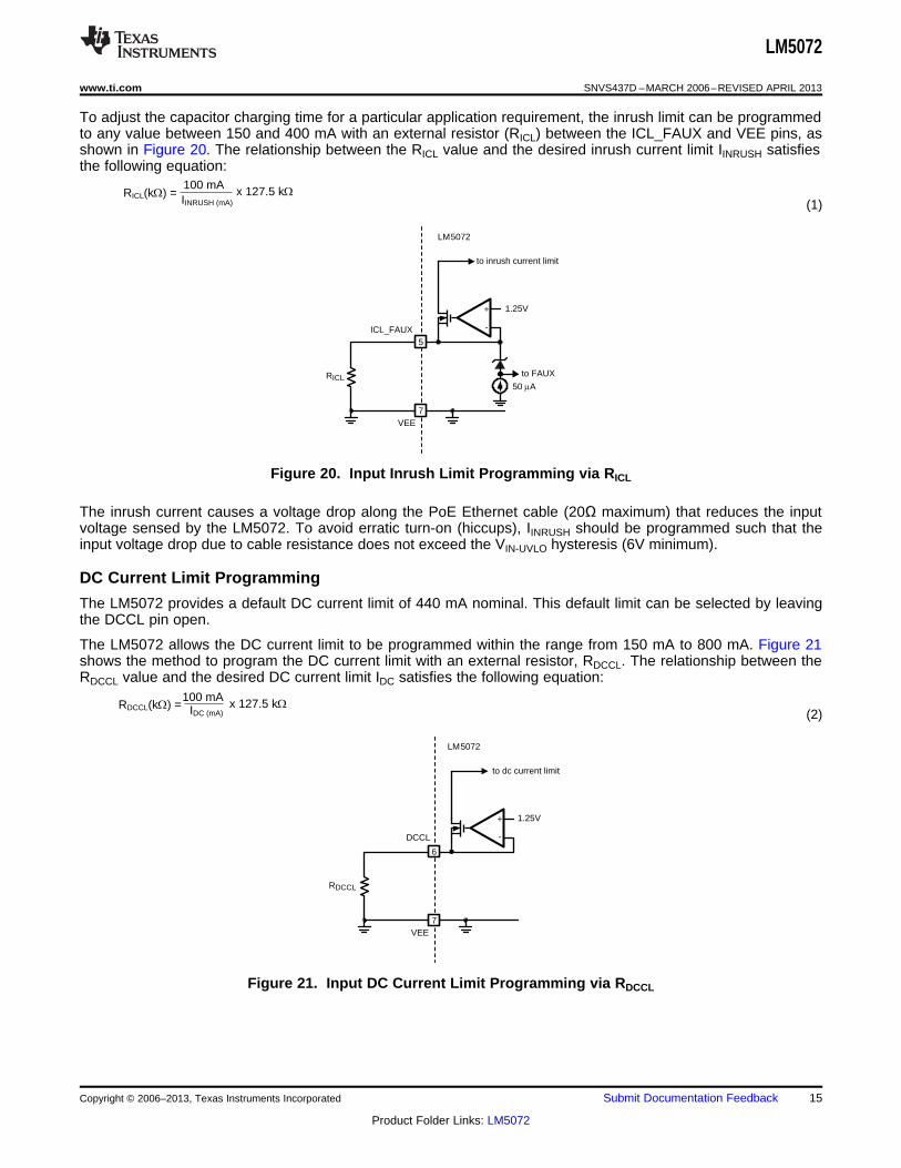
To adjust the capacitor charging time for a particular application requirement, the inrush limit can be programmedto any value between 150 and 400 mA with an external resistor (RICL) between the ICL_FAUX and VEE pins, asshown in Figure 20. The relationship between the RICL value and the desired inrush current limit IINRUSH satisfiesthe following equation:
(1)
Figure 20. Input Inrush Limit Programming via RICL
The inrush current causes a voltage drop along the PoE Ethernet cable (20Ω maximum) that reduces the inputvoltage sensed by the LM5072. To avoid erratic turn-on (hiccups), IINRUSH should be programmed such that theinput voltage drop due to cable resistance does not exceed the VIN-UVLO hysteresis (6V minimum).
DC Current Limit Programming
The LM5072 provides a default DC current limit of 440 mA nominal. This default limit can be selected by leavingthe DCCL pin open.
The LM5072 allows the DC current limit to be programmed within the range from 150 mA to 800 mA. Figure 21shows the method to program the DC current limit with an external resistor, RDCCL. The relationship between theRDCCL value and the desired DC current limit IDC satisfies the following equation:
(2)
Figure 21. Input DC Current Limit Programming via RDCCL
Copyright © 2006–2013, Texas Instruments Incorporated Submit Documentation Feedback 15
Product Folder Links: LM5072
+
-
11
10
VCC
nPGOOD
16
PWM DISABLE
LED to indicate
ARTN
50PA "Powered from PoE"
LM5072
130:
PG
OO
D
2.5V CPGOOD
RLED
LM5072
SNVS437D –MARCH 2006–REVISED APRIL 2013 www.ti.com
The maximum recommended DC current limit is 800 mA. While thermal analysis should be a standard part of themodule development process, it may warrant additional attention if the DC current limit is programmed to valuesin excess of 400 mA. This analysis should include evaluations of the dissipation capability of LM5072 package,heat sinking properties of the PC Board, ambient temperature, and other heat dissipation factors of the operatingenvironment.
Power Good and Regulator Startup
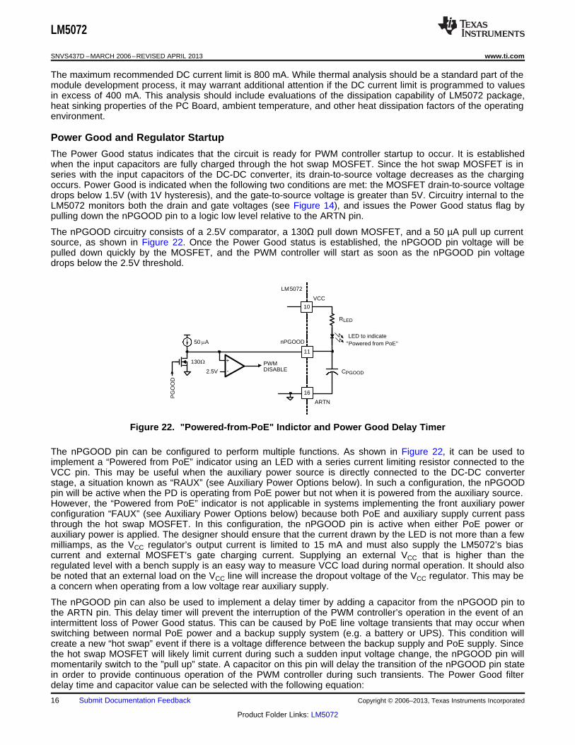
The Power Good status indicates that the circuit is ready for PWM controller startup to occur. It is establishedwhen the input capacitors are fully charged through the hot swap MOSFET. Since the hot swap MOSFET is inseries with the input capacitors of the DC-DC converter, its drain-to-source voltage decreases as the chargingoccurs. Power Good is indicated when the following two conditions are met: the MOSFET drain-to-source voltagedrops below 1.5V (with 1V hysteresis), and the gate-to-source voltage is greater than 5V. Circuitry internal to theLM5072 monitors both the drain and gate voltages (see Figure 14), and issues the Power Good status flag bypulling down the nPGOOD pin to a logic low level relative to the ARTN pin.
The nPGOOD circuitry consists of a 2.5V comparator, a 130Ω pull down MOSFET, and a 50 µA pull up currentsource, as shown in Figure 22. Once the Power Good status is established, the nPGOOD pin voltage will bepulled down quickly by the MOSFET, and the PWM controller will start as soon as the nPGOOD pin voltagedrops below the 2.5V threshold.
Figure 22. "Powered-from-PoE" Indictor and Power Good Delay Timer
The nPGOOD pin can be configured to perform multiple functions. As shown in Figure 22, it can be used toimplement a “Powered from PoE” indicator using an LED with a series current limiting resistor connected to theVCC pin. This may be useful when the auxiliary power source is directly connected to the DC-DC converterstage, a situation known as “RAUX” (see Auxiliary Power Options below). In such a configuration, the nPGOODpin will be active when the PD is operating from PoE power but not when it is powered from the auxiliary source.However, the “Powered from PoE” indicator is not applicable in systems implementing the front auxiliary powerconfiguration “FAUX” (see Auxiliary Power Options below) because both PoE and auxiliary supply current passthrough the hot swap MOSFET. In this configuration, the nPGOOD pin is active when either PoE power orauxiliary power is applied. The designer should ensure that the current drawn by the LED is not more than a fewmilliamps, as the VCC regulator’s output current is limited to 15 mA and must also supply the LM5072’s biascurrent and external MOSFET’s gate charging current. Supplying an external VCC that is higher than theregulated level with a bench supply is an easy way to measure VCC load during normal operation. It should alsobe noted that an external load on the VCC line will increase the dropout voltage of the VCC regulator. This may bea concern when operating from a low voltage rear auxiliary supply.
The nPGOOD pin can also be used to implement a delay timer by adding a capacitor from the nPGOOD pin tothe ARTN pin. This delay timer will prevent the interruption of the PWM controller’s operation in the event of anintermittent loss of Power Good status. This can be caused by PoE line voltage transients that may occur whenswitching between normal PoE power and a backup supply system (e.g. a battery or UPS). This condition willcreate a new “hot swap” event if there is a voltage difference between the backup supply and PoE supply. Sincethe hot swap MOSFET will likely limit current during such a sudden input voltage change, the nPGOOD pin willmomentarily switch to the ”pull up” state. A capacitor on this pin will delay the transition of the nPGOOD pin statein order to provide continuous operation of the PWM controller during such transients. The Power Good filterdelay time and capacitor value can be selected with the following equation:
16 Submit Documentation Feedback Copyright © 2006–2013, Texas Instruments Incorporated
Product Folder Links: LM5072
VIN
RAUX
VEE
OUT
RT
CS
FB
COMP
SS
RTN
ARTN
DCCL
RCLASS
nPGOOD
VCC
+PoE
+ FAUX
- FAUX
-PoE
ICL_FAUX
+VOUT
LM5072
0.1 PF
CPGOOD(nF) =0.05mA + ILED (mA)
1mA 0.25 msx
tPG_Delay (ms)x 100 nF
LM5072
www.ti.com SNVS437D –MARCH 2006–REVISED APRIL 2013
(3)
For example, selecting 1000 nF for CPGOOD, the delay time will be 50 ms if no LED is used and about 0.83 mswhen an LED, drawing 3 mA, is used. The delay required for continued operation will depend on the amplitude ofthe transient, the DC current limit, the load, and the total amount of input capacitance. Note that this delay doesnot ensure continued operation. If the hot swap MOSFET is in current limit for an extended period, it may causea thermal limit condition. This will result in a complete shutdown of the switching regulator, though no elements inthe system will be permanently damaged and normal operation will resume momentarily.
The Power Good status will also affect the default DC current limit. Should the sensed drain to source voltage ofthe hot swap MOSFET (from ARTN to VEE) exceed 2.5V, the LM5072 will increase the DC current limit from thedefault 440 mA to 540 mA, thus allowing the PD to continue operation through the transient event. This highercurrent limit will remain in effect until one of the following events occur:1. the duration of loss of Power Good status exceeds tPG_Delay, at which time the PWM controller will be
disabled,2. the increased power dissipation in the hot swap MOSFET causes a thermal limit condition as previously
discussed, or3. the MOSFET drain to source voltage falls below 1.5V to re-establish Power Good status. Under this
condition, the LM5072 will revert back to the default 440 mA DC current limit once Power Good status isrestored. Note that if the DC current limit has been programmed externally with RDCCL (see the DC CurrentLimit Programming section), the DC current limit will remain at the programmed level even when the PowerGood status is lost.
Auxiliary Power Options
The LM5072 based PD can receive power from auxiliary sources like AC adapters and solar cells in addition tothe PoE enabled network. This is a desirable feature when the total system power requirements exceed thePSE’s load capacity. Furthermore, with the auxiliary power option the PD can be used in a standard Ethernet(non-PoE) system.
For maximum versatility, the LM5072 accepts two different auxiliary power configurations. The first one, shown inFigure 23, is the front auxiliary (FAUX) configuration in which the auxiliary source is “diode OR’d” with the PoEpotential received from the Ethernet connector. The second configuration, shown in Figure 24, is the rearauxiliary (RAUX) option in which the auxiliary power bypasses the PoE interface and is connected directly to theinput of the DC-DC converter through a diode. The FAUX option is desirable if the auxiliary power voltage issimilar to the PoE input voltage. However, when the auxiliary supply voltage is much lower than the PoE inputvoltage, the RAUX option is more favorable because the current from the auxiliary supply is not limited by the hotswap MOSFET DC current limit. A comparison of the FAUX and RAUX options is presented in Table 3. Note theICL_FAUX and RAUX pins are not reverse voltage protected. If complete reverse protection is desired, seriesblocking diodes are necessary.
Figure 23. The FAUX Configuration
Copyright © 2006–2013, Texas Instruments Incorporated Submit Documentation Feedback 17
Product Folder Links: LM5072
VIN
RAUX
VEE
OUT
RT
CS
FB
COMP
SS
RTNARTN
ICL_ FAUX
DCCL
RCLASS
nPGOOD
VCC
+PoE
-RAUX
+RAUX
0.1 PF
LM5072
-PoE
+VOUT
LM5072
SNVS437D –MARCH 2006–REVISED APRIL 2013 www.ti.com
Figure 24. The RAUX Configuration
Table 3. Comparison Between FAUX and RAUX Operation
Tradeoff FAUX Operation RAUX Operation
Hot Swap Protection / Current Limit Automatically provided by the hot swap Requires a series resistor to limit the inrush currentProtection MOSFET. during hot swap.
Minimum Auxiliary Voltage Limited to 18V by the signature detection Only limited by 9V minimum input requirement.(at the IC pins) mode, or by the power requirement
(current limit).
Auxiliary Dominance Over PoE Cannot be forced without external Can be forced with appropriate RAUX pincomponents. configuration.
Use of nPGOOD Pin as “Powered from Not applicable as power is delivered Supported.PoE” Indicator through the hot swap interface in both
PoE and FAUX modes.
Transient Protection Excellent due to active MOSFET current Fair due to passive resistor current limit.limit.
The term “Auxiliary Dominance” mentioned in Table 3 means that when the auxiliary power source is connected,it will always power the PD regardless of the state of PoE power. “Aux dominance” is achievable only with theRAUX option, as noted in the table.
If the PD is not designed for aux dominance, either the FAUX or RAUX power sources will deliver power to thePD only under the following two conditions:1. If auxiliary power is applied before PoE power, it will prevent the PD’s detection by the PSE and will supply
power indefinitely. This occurs because the PoE input bridge rectifiers will be reverse biased, so no detectionsignature will be observed. Under this condition, when the auxiliary supply is removed, power will not bemaintained because it will take some time for the PSE to perform signature detection and classificationbefore it will supply power.
2. If auxiliary power is applied after PoE power is already present but has a higher voltage than PoE, it mayassume power delivery responsibility. Under the second case, if the supplied voltages are comparable, theload current may be shared inversely proportional to the respective output impedances of each supply. (Theoutput impedance of the PSE supply is increased by the cable series resistance).
If PoE power is applied first and has a higher voltage than the non-dominant aux power source, it will continuepowering the PD even when the aux power source becomes available. In this case, should PoE power beremoved, the auxiliary source will assume power delivery and supply the DC-DC loads without interruption.
18 Submit Documentation Feedback Copyright © 2006–2013, Texas Instruments Incorporated
Product Folder Links: LM5072
=18V - 4V
100 PA
VAUX - VRAUX
100 PA= 140 k:
LM5072
www.ti.com SNVS437D –MARCH 2006–REVISED APRIL 2013
If either FAUX or RAUX power is supplied prior to PoE power, it will prevent the recognition of the PD by thePSE. Consequently, continuity of power delivery cannot be ensured because the PoE supply will not be presentwhen auxiliary power is removed.
FAUX Option
With the FAUX option, the LM5072 hot swap MOSFET provides inrush and DC current limit protection for theauxiliary power source. To select the FAUX configuration for an auxiliary voltage lower than nominal PoEvoltages, the ICL_FAUX pin must be forced above its high threshold to override the VIN UVLO function. Notethat when the ICL_FAUX pin is pulled high to override VIN UVLO, it also overrides the inrush current limitprogrammed by RICL, if present. In this case, the inrush current will revert back to the default 150 mA limit.
Pulling up the ICL_FAUX pin will increase the default DC current limit to 540 mA. This increase in DC currentlimit is necessary because higher current is required to support the PD output power at the lower input potentialsobserved with auxiliary sources. In cases where the auxiliary supply voltage is comparable to the PoE voltage,there is no need to pull-up the ICL_FAUX pin to override VIN UVLO, and the default DC current limit remains at440 mA. However, if the DC current limit is externally programmed with RDCCL, the condition of the ICL_FAUX pinwill not affect the programmed DC current limit. In other words, programmed DC current limit can be considereda “hard limit” that will not vary in any configuration.
RAUX Option
The RAUX option is desirable when the auxiliary supply voltage is significantly lower than the PoE voltage orwhen aux dominance is desired. The inrush and DC current limits of the LM5072 do not protect or limit the RAUXpower source, and an additional resistor in the RAUX input path will be needed to provide transient protection.
To select the RAUX option without aux dominance, simply pull up the RAUX pin to the auxiliary power supplyvoltage through a high value resistor. Depending on the auxiliary supply voltage, the resistor value should beselected such that the current flowing into the RAUX pin is approximately 100 µA when the pin is mid-waybetween the lower and upper RAUX thresholds (approximately 4V). For example, with an 18V non-dominant rearauxiliary supply, the pull up resistor should be:
(4)
If the PSE load capacity is limited and insufficient, aux dominance will be a desired feature to off load PoE powerfor other PDs that do not have auxiliary power available. Aux dominance is achieved by pulling the RAUX pin upto the auxiliary supply voltage through a lower value (~5 kΩ) resistor that delivers at least 250 µA into the RAUXpin. When this higher RAUX current level is detected, the LM5072 shuts down the PD interface. In aux dominantmode, the auxiliary power source will supply the PD system as soon as it is applied. PD operation will not beinterrupted when the aux power source is connected. The PoE source may or may not actually be removed bythe PSE, although the DC current from the network cable is effectively reduced to zero (< 150 µA). IEEE 802.3afrequires the AC input impedance to be greater than 2 MΩ to ensure PoE power removal. This condition is notsatisfied when the auxiliary power source is applied. The PSE may remove power from a port based on thereduction in DC current. This is commonly known as DC Maintain Power Signature (DC MPS), a common featurein many PSE systems.
The high voltage startup regulator of the PWM controller does not have low dropout capability and will not beable to provide VCC when the potential from VIN to RTN is less than 14.5V (no external VCC load). In this case,the auxiliary voltage should supply VCC directly via diode OR-ing to ensure successful startup.
When using the RAUX configuration, the positive potential connection of the 0.1 µF signature capacitor should bemoved from VIN to RTN/ARTN as shown in Figure 24. This provides a high frequency, low impedance path forthe IC's substrate during rear auxiliary operation. Placing the capacitor here will not affect signature mode.
It should be noted that rear auxiliary non-dominance does not imply PoE dominance. PoE dominance is difficultto achieve in any PoE system if continuity of power is desired. When the PoE voltage appears, the PSE and PDinterface must continue delivering load current in addition to charging the input capacitor bank from the auxiliaryvoltage to the PoE voltage. The situation is further complicated by the fact that for a given delivered power level,the load current is much higher at the lower input voltages typically used in auxiliary supplies. As is the caseduring any inrush sequence, very high power is dissipated in the hot swap MOSFET. Consequently, attemptingto achieve inrush completion while delivering load current is highly ill advised. Lastly, current delivered to thesystem may be limited by the PSE, the PD, or both.
Copyright © 2006–2013, Texas Instruments Incorporated Submit Documentation Feedback 19
Product Folder Links: LM5072
I_leak
RpdICL_FAUX or
RAUX Pin
VEE or RTN
AUX Input VINFront or Rear
LM5072
SNVS437D –MARCH 2006–REVISED APRIL 2013 www.ti.com
A Note About FAUX and RAUX Pin False Input State Detection
The ICL_FAUX and RAUX pins are used to sense the presence of auxiliary power sources. The input voltage ofeach pin must remain low when the auxiliary power sources are absent. However, the Or-ing diodes feeding theauxiliary power are not ideal and leak reverse current that can flow from the PoE input to both the ICL_FAUXand RAUX pins. When PoE power is applied, these leakage currents may elevate the potentials of theICL_FAUX and RAUX pins to false logic states.
One of two failure modes may be observed when the power diode feeding the front auxiliary input leaksexcessively. First, the current may corrupt the inrush current limit programming, if that feature has beenimplemented. Second, the leakage current may elevate the voltage on the pin to the ICL_FAUX input threshold,which will force UVLO release. This would certainly interrupt any attempt by the LM5072 PD interface to performthe signature or classification functions.
When the power diode that feeds the rear auxiliary input leaks, the false signal could imply a rear auxiliary supplyis present. In this case, the internal hot swap MOSFET will be turned off. This would of course block PoE powerflow and cause the circuit to prevent startup.
This leakage problem at the control input pins can be easily solved. As shown in Figure 25, an additional pull-down resistor (Rpd) across each auxiliary power control input provides a path for the diode leakage current sothat it will not create false states on the ICL_FAUX or RAUX pins.
Figure 25. Bypassing Resistor – Prevents False ICL_FAUX and RAUX Pin Signaling
High Voltage Startup Regulator
The LM5072 contains a startup bias regulator that allows the VIN pin to be connected directly to PoE networkvoltages as high as 100V. The regulator output is connected to the VCC pin, providing an initial DC bias voltageof 7.7V nominal to start the PWM controller. The regulator is internally current limited to no less than 15 mA toprevent excessive power dissipation. For VCC voltage stability and noise immunity, a capacitor ranging between0.1 µF to 10 µF is required between the VCC and ARTN pins. Though the current capability of the regulatorexceeds the requirements of the IC, no external DC load drawing more than 3 mA should be applied to theoutput. A small amount of current for a “Powered from PoE” indicator LED (see Power Good and RegulatorStartup section) is acceptable. After the DC-DC converter reaches steady state operation, the VCC voltage istypically elevated by an auxiliary winding of the power transformer. The sustained VCC voltage should be greaterthan 8.1V to ensure the current supplied by the startup regulator is reduced to zero. Increasing the VCC pinvoltage above the regulation level of the startup regulator automatically disables the regulator, thus reducing thepower dissipation inside the LM5072. The power savings can be significant as many high voltage MOSFETsrequire a relatively large amount of gate charge and the gate drive current adds directly to the VCC current draw.
A VCC under-voltage lock-out circuit monitors the VCC voltage to prevent the PWM controller from operating asthe VCC voltage rises during startup or falls during shutdown. The PWM controller is enabled when the VCCvoltage rising edge exceeds 7.6V and disabled when the VCC voltage falling edge drops below 6.25V.
Error Amplifier
The LM5072 contains a wide-bandwidth, high-gain error amplifier to regulate the output voltage in non-isolatedapplications. The amplifier’s non-inverting input is set to a fixed reference voltage of 1.25V, while the invertinginput is connected to the FB pin. The open-drain output of the amplifier is connected to the COMP pin, which ispulled up internally through a 5 kΩ resistor to an internal 5V bias voltage. Feedback loop compensation can beeasily implemented by placing the compensation network, represented by “Zcomp”, between the FB and COMPpins as shown in Figure 26.
20 Submit Documentation Feedback Copyright © 2006–2013, Texas Instruments Incorporated
Product Folder Links: LM5072
CS
ARTN
RTN
OUT
R SENSE
1 nF
100:
LM5072
+ CLK LEBcurrent sense
65 ns blanking
To PWM Comparator
To Drain of Hot Swap MOSFET
12
9
16
8
Isolation
5k
COMP15
14
FB
SS
to PWM
16
ARTN
FromSecondary
Error-Amplifier
5V
.1 25V
LM5072Boundary
5k
COMP
15
14FB
SS
to PWM
R2
16ARTN
R1
Vo
Zcomp
5V
.1 25V
LM5072
LM5072
www.ti.com SNVS437D –MARCH 2006–REVISED APRIL 2013
Figure 26. Internal Error Amplifier – Used for Non-isolated Output Applications
For isolated applications, the error amplifier function is located on the isolated secondary side. The LM5072’serror amplifier can be disabled by connecting the FB pin to the ARTN pin. As shown in Figure 27, an opto-coupler is normally used to send the feedback signal across the isolation boundary to the COMP pin. Theinternal pull-up resistor on the COMP pin now serves as the pull-up bias for the opto-coupler transistor.
Figure 27. The Internal Error Amplifier – Bypassed in Isolated Output Applications
Current Sense and Limit
The LM5072 CS pin senses the transformer primary current signal for current mode control and current limiting ofthe supply. As shown in Figure 28, the current sense function can be fulfilled by a simple sense resistor RSENSEinserted between the RTN and the source of the primary MOSFET switch.
The RSENSE resistor should be non-inductive, and a low pass filter should be used to reject the switching noise onthe sensed signal. A simple RC filter using 100Ω and 1 nF is typically sufficient. The filter capacitor must belocated close to the CS and ARTN pins. In order to prevent noise propagation and to improve the noise immunityof the current sense, it is very important to minimize the return path of the current sense signal. This isaccomplished with direct connection to the ARTN pin and a single point connection to the RTN pin on the PCBoard layout.
Figure 28. Current Sense Schemes
Copyright © 2006–2013, Texas Instruments Incorporated Submit Documentation Feedback 21
Product Folder Links: LM5072
FOSC (kHz)x 26.2 k:RT(k:) =
200 kHz
Leading Edge Narrow Spike
LM5072
SNVS437D –MARCH 2006–REVISED APRIL 2013 www.ti.com
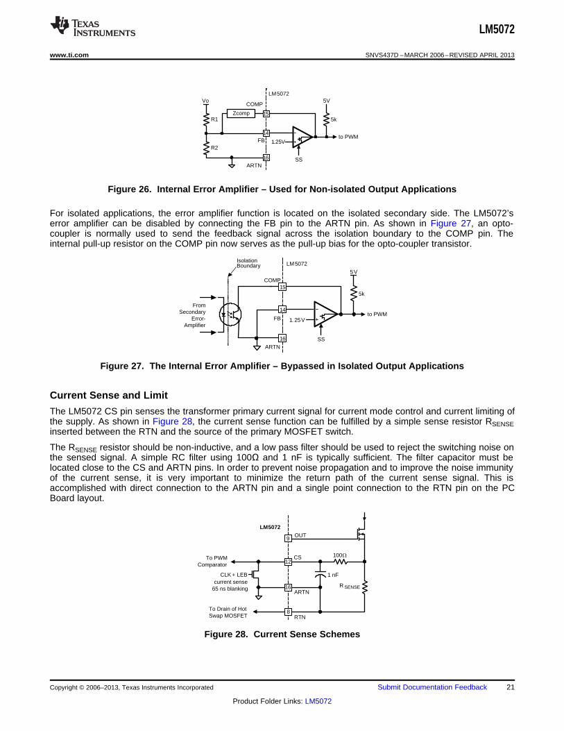
Figure 29. Typical Current Sense Waveform Having a Leading Edge Spike
The current sense signal is also used for cycle-by-cycle over-current protection. When the CS pin signal exceeds0.5V, the PWM pulse of that cycle will be immediately terminated. The desired cycle-by-cycle over-currentprotection level is achieved by selecting the proper value of current sense resistor that produces 0.5V at the CSpin. For the LM5072-80, the slope compensation reduces the current limit threshold by about 20% maximum atthe 80% maximum duty cycle.
The typical current sense waveform as shown in Figure 29 has a spike at the leading edge. This spike is mainlycaused by the large gate drive current that flows through the current sense resistor at turn-on (up to 0.8A). Thereverse recovery of the rectifier diode on the secondary side and the cross conduction of the primary MOSFETand sync MOSFET (if used) may also contribute to this leading edge spike. With a relatively small external RCfilter, this spike can still cause a false over-current condition that terminates the PWM output pulse. To avoid thisproblem, an internal blanking circuit is provided within the LM5072 as shown in Figure 28. An internal MOSFETis turned on to short the CS pin to ARTN at the end of each cycle. This MOSFET switch remains on for anadditional 65ns after the beginning of the next PWM cycle, thus blanking out the leading edge spike on thecurrent sense signal.
Soft-Start
The LM5072 incorporates a soft-start feature which forces the PWM duty cycle to grow progressively duringstartup such that the output voltage increases gradually to the steady state level. The soft-start process reducesor prevents both the surge of inrush current and the associated overshoot of the output voltage during startup.The LM5072 achieves soft-start using an internal 10 µA current source to charge an external capacitorconnected to the SS pin. The capacitor voltage limits the voltage at the COMP pin which directly controls thePWM duty cycle. The rate of the soft-start ramp can be adjusted by varying the value of the external capacitor.Note that the slope of the supply’s output voltage is influenced by the load condition and the total outputcapacitance of the supply, as well as the soft-start programming. The supply should be started slowly enoughsuch that the input current is limited below the hot swap MOSFET DC current limit.
Gate Driver and Maximum Duty Cycle Limit
The LM5072’s gate drive (OUT) pin can source and sink a peak current of 800 mA directly to the gate of the DC-DC converter’s power MOSFET switch. To serve a variety of applications, the LM5072 is available with twooptions for maximum PWM duty cycle. The LM5072-80 operates at duty cycles up to 80% while the LM5072-50limits the PWM duty cycle to 50%.
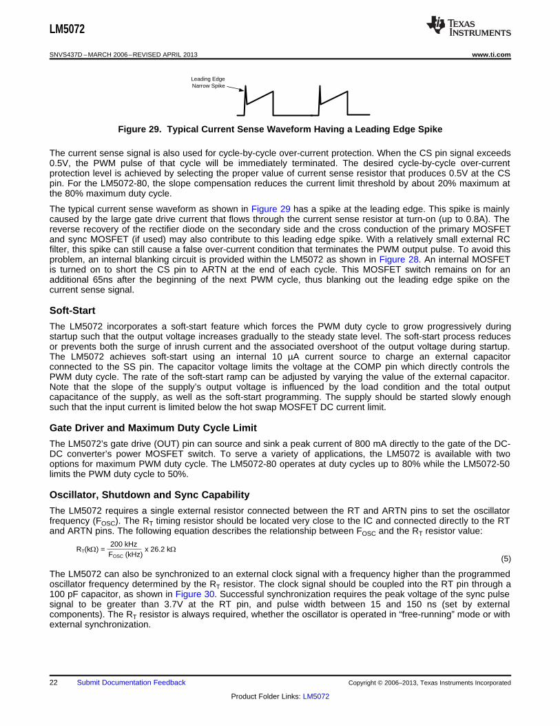
Oscillator, Shutdown and Sync Capability
The LM5072 requires a single external resistor connected between the RT and ARTN pins to set the oscillatorfrequency (FOSC). The RT timing resistor should be located very close to the IC and connected directly to the RTand ARTN pins. The following equation describes the relationship between FOSC and the RT resistor value:
(5)
The LM5072 can also be synchronized to an external clock signal with a frequency higher than the programmedoscillator frequency determined by the RT resistor. The clock signal should be coupled into the RT pin through a100 pF capacitor, as shown in Figure 30. Successful synchronization requires the peak voltage of the sync pulsesignal to be greater than 3.7V at the RT pin, and pulse width between 15 and 150 ns (set by externalcomponents). The RT resistor is always required, whether the oscillator is operated in “free-running” mode or withexternal synchronization.
22 Submit Documentation Feedback Copyright © 2006–2013, Texas Instruments Incorporated
Product Folder Links: LM5072
RTto Clock 1
ARTN
RT Synch Pulse
LM5072100 pF
16
LM5072
www.ti.com SNVS437D –MARCH 2006–REVISED APRIL 2013
Figure 30. Oscillator Synchronization Implementation
Special attention should be paid to the relationship between the oscillator frequency and the PWM switchingfrequency. For the LM5072-50 version, the programmed oscillator frequency is internally divided by two in orderto facilitate the 50% duty cycle limit. The PWM output switching frequency is therefore one half of theprogrammed oscillator frequency. The frequency divider is not used in the LM5072-80 and therefore the PWMoutput frequency is the same as the oscillator frequency. These relationships also apply to externalsynchronization frequency versus PWM output frequency.
PWM Comparator / Slope Compensation
The PWM comparator produces the PWM duty cycle by comparing the current sense ramp signal with an errorvoltage derived from the error amplifier output. The error amplifier output voltage at the COMP pin is offset by1.4V and then further attenuated by a 3:1 resistor divider before it is presented to the PWM comparator input.
The PWM duty cycle increases with the voltage at the COMP pin. The controller output duty cycle reduces tozero when the COMP pin voltage drops below approximately 1.4V.
For duty cycles greater than 50%, current mode control loops are subject to sub-harmonic oscillation. Thisinstability can be eliminated by adding an additional fixed slope voltage ramp signal to the current sense signal.This technique is commonly known as “slope compensation”. For the LM5072-80 version with its maximum dutycycle of 80%, slope compensation is integrated by injecting a 45 μA current ramp from the oscillator into thecurrent sense signal path (see Figure 15). The 45 μA peak ramping current flows through an internal 2 kΩresistor to produce a fixed voltage ramp at the PWM comparator input. Additional slope compensation may beadded by increasing the source impedance of the current sense signal with an external resistor between the CSpin and the source of the current sense signal. The feature is disabled for the LM5072-50 version because theduty cycle is limited to 50% and slope compensation is not required.
Thermal Protection
The LM5072 includes internal thermal shutdown circuitry to protect the IC in the event the maximum junctiontemperature is exceeded. This circuit prevents catastrophic overheating due to accidental overload of the hotswap MOSFET or other circuitry. Typically, thermal shutdown is activated at 165°C, causing the hot swapMOSFET and classification regulator to be disabled. The PWM controller is disabled after the PGOOD timer hasexpired. Thermal limit is not enabled unless the module is being powered through the front end and the hot swapMOSFET is enhanced. VCC current limit provides an adequate level of protection for this 15 mA regulator. Thethermal protection is non-latching, therefore after the temperature drops by the 25°C nominal hysteresis, the hotswap MOSFET is re-activated and a soft-start is initiated to restore the LM5072 to normal operation. If the causeof overheating has not been eliminated, the circuit will hiccup in and out of the thermal shutdown mode.
PCB Layout Guidelines
Before processing the Printed Circuit Board (PCB) layout, the engineer should make all necessary adjustmentsto the schematic to suite the application. The reader may notice that the LM5072 evaluation board is designedwith dual outputs, both FAUX and RAUX power options, and some re-configuration flexibility features (refer toFigure 32). However, many devices can be removed for a particular application. Recommendations onsimplifying Figure 32 to suit a given application are as follows:1. When selecting the FAUX power option only, delete C3, D1, D2, J3, P3, P4, R1, R2, R13, and R29.2. When selecting the RAUX power option only, delete R30, D3, D7, J2, P1, P2 and R6.3. When neither FAUX nor RAUX power options are selected, delete all the parts mentioned in (1) and (2)
above.4. When only a single output is required, delete C11 through C14, C17, D8, J6, J7, L2, R10 and Z4. Modify T1
design to delete the unwanted second output winding and increase the copper used for the single output
Copyright © 2006–2013, Texas Instruments Incorporated Submit Documentation Feedback 23
Product Folder Links: LM5072
LM5072
SNVS437D –MARCH 2006–REVISED APRIL 2013 www.ti.com
winding. This re-configuration should make use of the spare pins of the transformer.5. R24 should be deleted from the schematic completely, being replaced by a short connection for an isolated
application, or by an open for a non-isolated application.6. Jumpers P5 and P6 (Figure 33) should be deleted from the schematic completely, being replaced by a short
connection for an isolated application, or by an open for a non-isolated application.7. When the output is non-isolated, delete C20, C22, C25, R7, R11, R16, R17, R24, U2, and U3. Replace C28
with a short connection, and replace P5 and P6 with short connections.8. One may also modify the number of input and output capacitors to achieve a more optimized design.
Consider the following when starting the PCB design:1. Try to use both sides of the PCB for part placement to facilitate both layout and routing.2. Place the power components in a pattern that minimizes the lengths of the high current paths on the PCB.3. Place the LM5072 and its critical peripheral parts closely. Bypass capacitors and transient protection
elements should be near the LM5072.4. Route the critical traces first, including both power and signal traces. Make the length of the trace as short as
possible, and avoid excessive use of via holes.5. Pay attention to grounding issues. Each reference ground should be a copper plane or island. Use via holes
if necessary for direct connections of devices to their appropriate return ground plane or island. Identify thefollowing ground returns:– Primary power return COM: C4, C5, C6, R14, R15, R29, C3, P4, J3-pins 2 and 3, U1-pin 8, C28, and
C29 are all returned to the COM ground plane.– Primary control signal return, a ground return island: C19, T1-pin 2, C23, U2-pin 3, R24, C26, C21, and
U1-pin 16 are all returned to this island, and the island should be single point connected to the COMground plane.
– Secondary power return IGND: T1-pins 6 and 7, C7 through C10, C12 through C17, C28, Z4, J5, andJ7 are all returned to the IGND ground plane.
– Secondary control signal return, a ground return island: R18, U3 and C20 are all returned to this island,and the island should be single point connected to the IGND ground plane.
Also consider the following during PCB layout and routing.1. Place the following power components in each group as close as possible:
– C4, C5 (if used), the primary winding of T1, Q1, and R14/R15. The high frequency switching current(pulse current) flows through these parts in a loop. The physical area enclosed by the loop should be assmall as possible.
– D5, C7 through C10, and the secondary winding of T1 for the main output. The high frequencyswitching current for the main output rail flows through these parts in a loop. The physical area enclosedby the loop should be as small as possible.
– D8, C12 and C13, and the secondary winding of T1 for the second output, if used. The high frequencyswitching current for the second output rail flows through these parts in a loop. The physical areaenclosed by the loop should be as small as possible.
– L3, C15, C16, J4 and J5 (if posts are used). L3 should also be as close as possible to the capacitorbank consisting of C7 through C10 in order to minimize the conduction losses on the PCB. Ceramiccapacitor C15 should be placed directly at the output port.
– L2, C14, C17, Z4, J6 and J7 (if posts are used) for the second output rail. L2 should also be as closeas possible to C12 and C13 in order to minimize the conduction losses on the PCB. Ceramic capacitorC14 should be directly placed at the output port
2. U1 (LM5072) should be placed close to Q1 in the orientation such that the gate drive output pin (OUT, Pin 9)is close to Q1’s gate.
3. Z2 and C27 must be placed directly across the VIN and VEE pins for best protection against input transients.In a rear auxiliary application, C27 should be removed and C29 should be installed very close to the RTNand VEE pins.
4. C19 should be placed directly across the VCC and ARTN pins.5. C23 should be placed directly across the CS and ARTN pins.6. R21 should be placed directly across the RT and ARTN pins.
24 Submit Documentation Feedback Copyright © 2006–2013, Texas Instruments Incorporated
Product Folder Links: LM5072

LM5072
www.ti.com SNVS437D –MARCH 2006–REVISED APRIL 2013
7. C26 should be placed directly across the SS and ARTN pins.8. C21 should be placed directly across the nPGOOD and ARTN pins.9. R25 should be directly routed from the output port.10. R9 should be directly routed from R14/R15.11. D6 and Z1 should be placed to achieve the shortest connection from C4 or C5 to the drain pad(s) of Q1 for
better snubbing.12. C2 and R4 should be placed to achieve the shortest connection across D5.13. Q1, D5, D8, and U1 (LM5072) should be installed on thermal pads having adequate thermal vias down
through all PCB Layers and an exposed thermal pad on the other side of the PCB.14. Avoid spiral trace pattern.15. Avoid placing switching traces near any traces in the regulator feedback loop.16. Pay attention to trace width. Try to make the power traces as wide as possible. Conversely, do not make
signal traces wider than needed.
After the first placement and routing is completed, make necessary modifications to optimize the design.
Application Example #1
Figure 31 shows an application example of a single isolated output solution for the PD. Both front auxiliary(FAUX) and rear auxiliary (RAUX) power options are given, although only one option may be needed in practice.Note that for the RAUX option, D2 is only installed when the supply voltage of the auxiliary power source wouldcause the VIN voltage to be below 14.5V.
Figure 31. PD with Isolated, Single Output Solution
Copyright © 2006–2013, Texas Instruments Incorporated Submit Documentation Feedback 25
Product Folder Links: LM5072

LM5072
SNVS437D –MARCH 2006–REVISED APRIL 2013 www.ti.com
Application Example #2
Figure 32 shows an example of an isolated, dual-output solution for the PD. The 3.3V output is tightly regulatedwhile the 5V output is cross-regulated. Both front auxiliary (FAUX) and rear auxiliary (RAUX) power options aregiven, although only one option may be needed in practice. Note that for the RAUX option, D2 is only installedwhen the supply voltage of the auxiliary power source is lower than 14.5V.
Figure 32. PD with Isolated, Dual Output Solution
26 Submit Documentation Feedback Copyright © 2006–2013, Texas Instruments Incorporated
Product Folder Links: LM5072
LM5072
www.ti.com SNVS437D –MARCH 2006–REVISED APRIL 2013
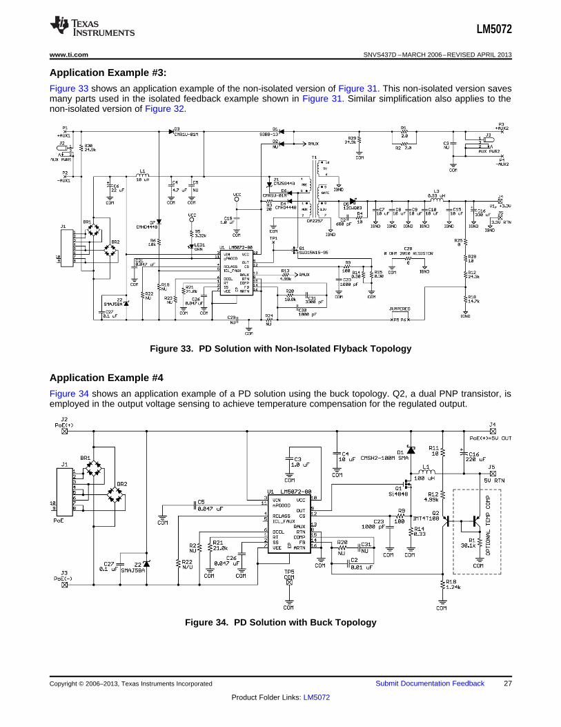
Application Example #3:
Figure 33 shows an application example of the non-isolated version of Figure 31. This non-isolated version savesmany parts used in the isolated feedback example shown in Figure 31. Similar simplification also applies to thenon-isolated version of Figure 32.
Figure 33. PD Solution with Non-Isolated Flyback Topology
Application Example #4
Figure 34 shows an application example of a PD solution using the buck topology. Q2, a dual PNP transistor, isemployed in the output voltage sensing to achieve temperature compensation for the regulated output.
Figure 34. PD Solution with Buck Topology
Copyright © 2006–2013, Texas Instruments Incorporated Submit Documentation Feedback 27
Product Folder Links: LM5072
LM5072
SNVS437D –MARCH 2006–REVISED APRIL 2013 www.ti.com
REVISION HISTORY
Changes from Revision C (April 2013) to Revision D Page
• Changed layout of National Data Sheet to TI format .......................................................................................................... 27
28 Submit Documentation Feedback Copyright © 2006–2013, Texas Instruments Incorporated
Product Folder Links: LM5072
PACKAGE OPTION ADDENDUM
www.ti.com 27-Oct-2016
Addendum-Page 1
PACKAGING INFORMATION
Orderable Device Status(1)
Package Type PackageDrawing
Pins PackageQty
Eco Plan(2)
Lead/Ball Finish(6)
MSL Peak Temp(3)
Op Temp (°C) Device Marking(4/5)
Samples
LM5072MH-80/NOPB ACTIVE HTSSOP PWP 16 92 Green (RoHS& no Sb/Br)
CU SN Level-1-260C-UNLIM -40 to 125 LM5072MH-80
LM5072MHX-80/NOPB ACTIVE HTSSOP PWP 16 2500 Green (RoHS& no Sb/Br)
CU SN Level-1-260C-UNLIM -40 to 125 LM5072MH-80
(1) The marketing status values are defined as follows:ACTIVE: Product device recommended for new designs.LIFEBUY: TI has announced that the device will be discontinued, and a lifetime-buy period is in effect.NRND: Not recommended for new designs. Device is in production to support existing customers, but TI does not recommend using this part in a new design.PREVIEW: Device has been announced but is not in production. Samples may or may not be available.OBSOLETE: TI has discontinued the production of the device.
(2) Eco Plan - The planned eco-friendly classification: Pb-Free (RoHS), Pb-Free (RoHS Exempt), or Green (RoHS & no Sb/Br) - please check http://www.ti.com/productcontent for the latest availabilityinformation and additional product content details.TBD: The Pb-Free/Green conversion plan has not been defined.Pb-Free (RoHS): TI's terms "Lead-Free" or "Pb-Free" mean semiconductor products that are compatible with the current RoHS requirements for all 6 substances, including the requirement thatlead not exceed 0.1% by weight in homogeneous materials. Where designed to be soldered at high temperatures, TI Pb-Free products are suitable for use in specified lead-free processes.Pb-Free (RoHS Exempt): This component has a RoHS exemption for either 1) lead-based flip-chip solder bumps used between the die and package, or 2) lead-based die adhesive used betweenthe die and leadframe. The component is otherwise considered Pb-Free (RoHS compatible) as defined above.Green (RoHS & no Sb/Br): TI defines "Green" to mean Pb-Free (RoHS compatible), and free of Bromine (Br) and Antimony (Sb) based flame retardants (Br or Sb do not exceed 0.1% by weightin homogeneous material)
(3) MSL, Peak Temp. - The Moisture Sensitivity Level rating according to the JEDEC industry standard classifications, and peak solder temperature.
(4) There may be additional marking, which relates to the logo, the lot trace code information, or the environmental category on the device.
(5) Multiple Device Markings will be inside parentheses. Only one Device Marking contained in parentheses and separated by a "~" will appear on a device. If a line is indented then it is a continuationof the previous line and the two combined represent the entire Device Marking for that device.
(6) Lead/Ball Finish - Orderable Devices may have multiple material finish options. Finish options are separated by a vertical ruled line. Lead/Ball Finish values may wrap to two lines if the finishvalue exceeds the maximum column width.
Important Information and Disclaimer:The information provided on this page represents TI's knowledge and belief as of the date that it is provided. TI bases its knowledge and belief on informationprovided by third parties, and makes no representation or warranty as to the accuracy of such information. Efforts are underway to better integrate information from third parties. TI has taken andcontinues to take reasonable steps to provide representative and accurate information but may not have conducted destructive testing or chemical analysis on incoming materials and chemicals.TI and TI suppliers consider certain information to be proprietary, and thus CAS numbers and other limited information may not be available for release.
PACKAGE OPTION ADDENDUM
www.ti.com 27-Oct-2016
Addendum-Page 2
In no event shall TI's liability arising out of such information exceed the total purchase price of the TI part(s) at issue in this document sold by TI to Customer on an annual basis.
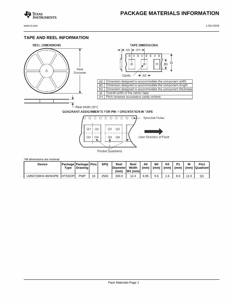
TAPE AND REEL INFORMATION
*All dimensions are nominal
Device PackageType
PackageDrawing
Pins SPQ ReelDiameter
(mm)
ReelWidth
W1 (mm)
A0(mm)
B0(mm)
K0(mm)
P1(mm)
W(mm)
Pin1Quadrant
LM5072MHX-80/NOPB HTSSOP PWP 16 2500 330.0 12.4 6.95 5.6 1.6 8.0 12.0 Q1
PACKAGE MATERIALS INFORMATION
www.ti.com 1-Oct-2016
Pack Materials-Page 1
*All dimensions are nominal
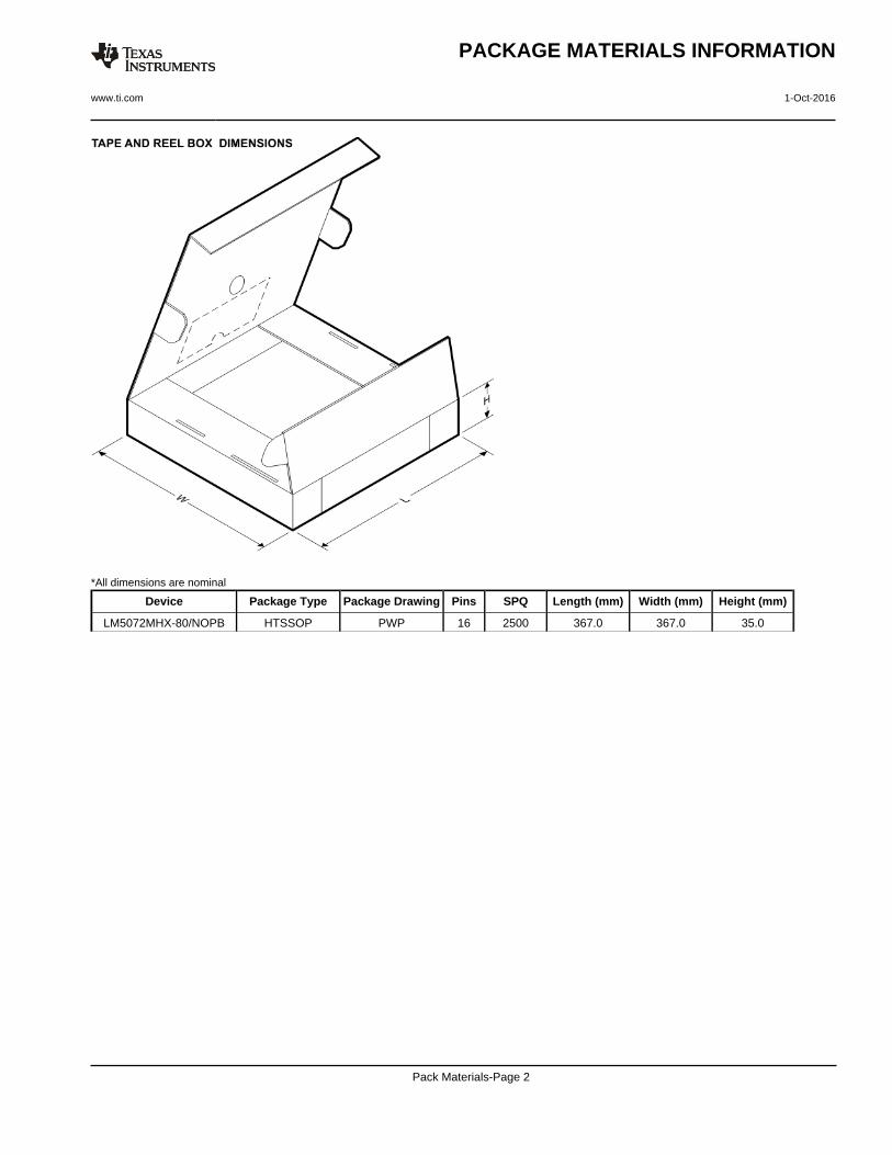
Device Package Type Package Drawing Pins SPQ Length (mm) Width (mm) Height (mm)
LM5072MHX-80/NOPB HTSSOP PWP 16 2500 367.0 367.0 35.0
PACKAGE MATERIALS INFORMATION
www.ti.com 1-Oct-2016
Pack Materials-Page 2
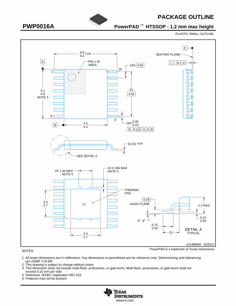
www.ti.com
PACKAGE OUTLINE
C
TYP6.66.2
14X 0.65
16X 0.300.19
2X4.55
(0.15) TYP
0 - 80.150.05
3.32.7
3.32.7
2X 1.34 MAXNOTE 5
1.2 MAX
(1)
0.25GAGE PLANE
0.750.50
A
NOTE 3
5.14.9
B 4.54.3
4X 0.166 MAXNOTE 5
4214868/A 02/2017
PowerPAD HTSSOP - 1.2 mm max heightPWP0016APLASTIC SMALL OUTLINE
NOTES: 1. All linear dimensions are in millimeters. Any dimensions in parenthesis are for reference only. Dimensioning and tolerancing per ASME Y14.5M. 2. This drawing is subject to change without notice. 3. This dimension does not include mold flash, protrusions, or gate burrs. Mold flash, protrusions, or gate burrs shall not exceed 0.15 mm per side.4. Reference JEDEC registration MO-153.5. Features may not be present.
PowerPAD is a trademark of Texas Instruments.
TM
116
0.1 C A B
98
PIN 1 IDAREA
SEATING PLANE
0.1 C
SEE DETAIL A
DETAIL ATYPICAL
SCALE 2.400
THERMALPAD
17
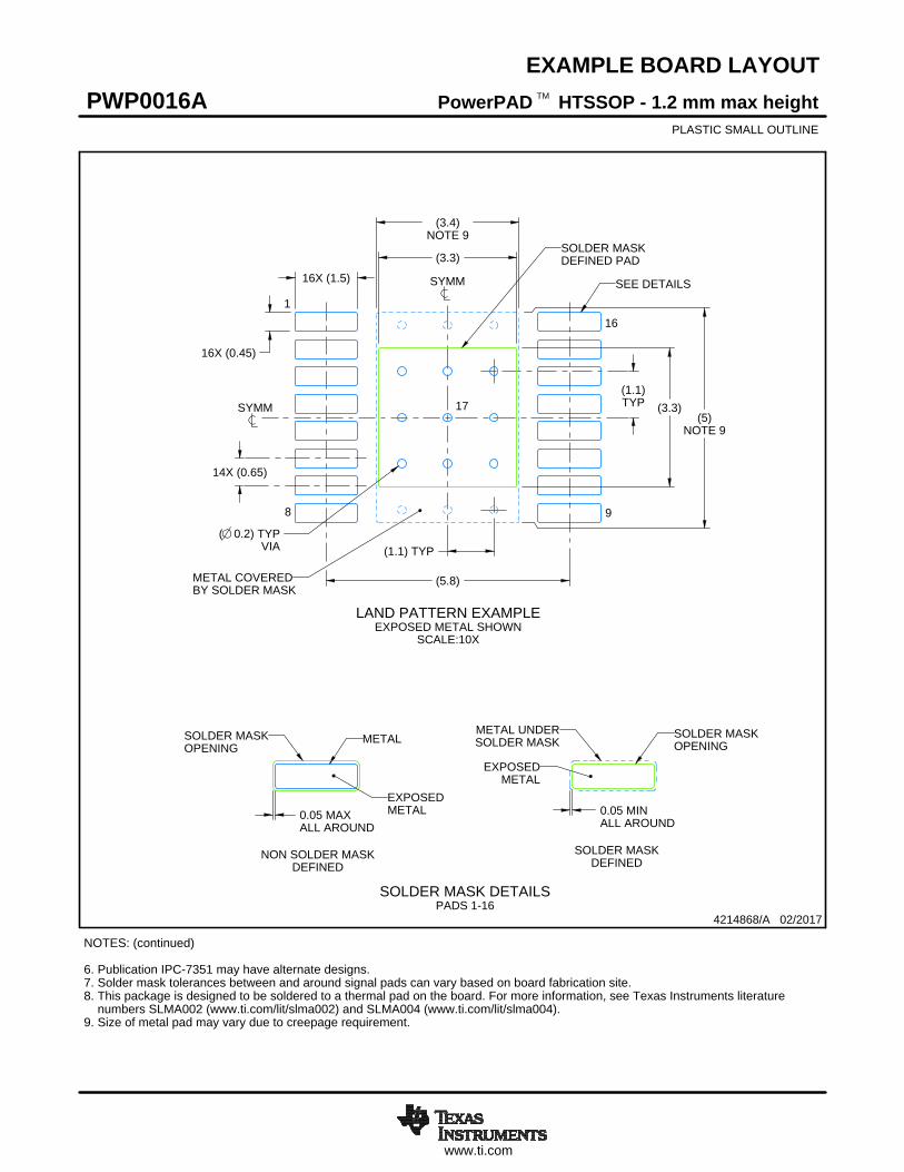
www.ti.com
EXAMPLE BOARD LAYOUT
(5.8)
0.05 MAXALL AROUND
0.05 MINALL AROUND
16X (1.5)
16X (0.45)
14X (0.65)
(3.4)NOTE 9
(5)NOTE 9
(3.3)
(3.3)
( 0.2) TYPVIA (1.1) TYP
(1.1)TYP
4214868/A 02/2017
PowerPAD HTSSOP - 1.2 mm max heightPWP0016APLASTIC SMALL OUTLINE
SYMM
SYMM
SEE DETAILS
LAND PATTERN EXAMPLEEXPOSED METAL SHOWN
SCALE:10X
1
8 9
16
METAL COVEREDBY SOLDER MASK
SOLDER MASKDEFINED PAD
17
NOTES: (continued) 6. Publication IPC-7351 may have alternate designs. 7. Solder mask tolerances between and around signal pads can vary based on board fabrication site. 8. This package is designed to be soldered to a thermal pad on the board. For more information, see Texas Instruments literature numbers SLMA002 (www.ti.com/lit/slma002) and SLMA004 (www.ti.com/lit/slma004).9. Size of metal pad may vary due to creepage requirement.
TM
METALSOLDER MASKOPENING
NON SOLDER MASKDEFINED
SOLDER MASK DETAILSPADS 1-16
EXPOSEDMETAL
SOLDER MASKDEFINED
SOLDER MASKMETAL UNDER SOLDER MASK
OPENING
EXPOSEDMETAL
www.ti.com
EXAMPLE STENCIL DESIGN
16X (1.5)
16X (0.45)
(3.3)
(3.3)BASED ON
0.125 THICKSTENCIL
14X (0.65)
(R0.05) TYP
(5.8)
4214868/A 02/2017
PowerPAD HTSSOP - 1.2 mm max heightPWP0016APLASTIC SMALL OUTLINE
2.79 X 2.790.1753.01 X 3.010.15
3.3 X 3.3 (SHOWN)0.1253.69 X 3.690.1
SOLDER STENCILOPENING
STENCILTHICKNESS
NOTES: (continued) 10. Laser cutting apertures with trapezoidal walls and rounded corners may offer better paste release. IPC-7525 may have alternate design recommendations. 11. Board assembly site may have different recommendations for stencil design.
TM
SYMM
SYMM
1
89
16
BASED ON0.125 THICK
STENCIL
BY SOLDER MASKMETAL COVERED
SEE TABLE FORDIFFERENT OPENINGSFOR OTHER STENCILTHICKNESSES
SOLDER PASTE EXAMPLEEXPOSED PAD
100% PRINTED SOLDER COVERAGE BY AREASCALE:10X
17
IMPORTANT NOTICE
Texas Instruments Incorporated (TI) reserves the right to make corrections, enhancements, improvements and other changes to itssemiconductor products and services per JESD46, latest issue, and to discontinue any product or service per JESD48, latest issue. Buyersshould obtain the latest relevant information before placing orders and should verify that such information is current and complete.TI’s published terms of sale for semiconductor products (http://www.ti.com/sc/docs/stdterms.htm) apply to the sale of packaged integratedcircuit products that TI has qualified and released to market. Additional terms may apply to the use or sale of other types of TI products andservices.Reproduction of significant portions of TI information in TI data sheets is permissible only if reproduction is without alteration and isaccompanied by all associated warranties, conditions, limitations, and notices. TI is not responsible or liable for such reproduceddocumentation. Information of third parties may be subject to additional restrictions. Resale of TI products or services with statementsdifferent from or beyond the parameters stated by TI for that product or service voids all express and any implied warranties for theassociated TI product or service and is an unfair and deceptive business practice. TI is not responsible or liable for any such statements.Buyers and others who are developing systems that incorporate TI products (collectively, “Designers”) understand and agree that Designersremain responsible for using their independent analysis, evaluation and judgment in designing their applications and that Designers havefull and exclusive responsibility to assure the safety of Designers' applications and compliance of their applications (and of all TI productsused in or for Designers’ applications) with all applicable regulations, laws and other applicable requirements. Designer represents that, withrespect to their applications, Designer has all the necessary expertise to create and implement safeguards that (1) anticipate dangerousconsequences of failures, (2) monitor failures and their consequences, and (3) lessen the likelihood of failures that might cause harm andtake appropriate actions. Designer agrees that prior to using or distributing any applications that include TI products, Designer willthoroughly test such applications and the functionality of such TI products as used in such applications.TI’s provision of technical, application or other design advice, quality characterization, reliability data or other services or information,including, but not limited to, reference designs and materials relating to evaluation modules, (collectively, “TI Resources”) are intended toassist designers who are developing applications that incorporate TI products; by downloading, accessing or using TI Resources in anyway, Designer (individually or, if Designer is acting on behalf of a company, Designer’s company) agrees to use any particular TI Resourcesolely for this purpose and subject to the terms of this Notice.TI’s provision of TI Resources does not expand or otherwise alter TI’s applicable published warranties or warranty disclaimers for TIproducts, and no additional obligations or liabilities arise from TI providing such TI Resources. TI reserves the right to make corrections,enhancements, improvements and other changes to its TI Resources. TI has not conducted any testing other than that specificallydescribed in the published documentation for a particular TI Resource.Designer is authorized to use, copy and modify any individual TI Resource only in connection with the development of applications thatinclude the TI product(s) identified in such TI Resource. NO OTHER LICENSE, EXPRESS OR IMPLIED, BY ESTOPPEL OR OTHERWISETO ANY OTHER TI INTELLECTUAL PROPERTY RIGHT, AND NO LICENSE TO ANY TECHNOLOGY OR INTELLECTUAL PROPERTYRIGHT OF TI OR ANY THIRD PARTY IS GRANTED HEREIN, including but not limited to any patent right, copyright, mask work right, orother intellectual property right relating to any combination, machine, or process in which TI products or services are used. Informationregarding or referencing third-party products or services does not constitute a license to use such products or services, or a warranty orendorsement thereof. Use of TI Resources may require a license from a third party under the patents or other intellectual property of thethird party, or a license from TI under the patents or other intellectual property of TI.TI RESOURCES ARE PROVIDED “AS IS” AND WITH ALL FAULTS. TI DISCLAIMS ALL OTHER WARRANTIES ORREPRESENTATIONS, EXPRESS OR IMPLIED, REGARDING RESOURCES OR USE THEREOF, INCLUDING BUT NOT LIMITED TOACCURACY OR COMPLETENESS, TITLE, ANY EPIDEMIC FAILURE WARRANTY AND ANY IMPLIED WARRANTIES OFMERCHANTABILITY, FITNESS FOR A PARTICULAR PURPOSE, AND NON-INFRINGEMENT OF ANY THIRD PARTY INTELLECTUALPROPERTY RIGHTS. TI SHALL NOT BE LIABLE FOR AND SHALL NOT DEFEND OR INDEMNIFY DESIGNER AGAINST ANY CLAIM,INCLUDING BUT NOT LIMITED TO ANY INFRINGEMENT CLAIM THAT RELATES TO OR IS BASED ON ANY COMBINATION OFPRODUCTS EVEN IF DESCRIBED IN TI RESOURCES OR OTHERWISE. IN NO EVENT SHALL TI BE LIABLE FOR ANY ACTUAL,DIRECT, SPECIAL, COLLATERAL, INDIRECT, PUNITIVE, INCIDENTAL, CONSEQUENTIAL OR EXEMPLARY DAMAGES INCONNECTION WITH OR ARISING OUT OF TI RESOURCES OR USE THEREOF, AND REGARDLESS OF WHETHER TI HAS BEENADVISED OF THE POSSIBILITY OF SUCH DAMAGES.Unless TI has explicitly designated an individual product as meeting the requirements of a particular industry standard (e.g., ISO/TS 16949and ISO 26262), TI is not responsible for any failure to meet such industry standard requirements.Where TI specifically promotes products as facilitating functional safety or as compliant with industry functional safety standards, suchproducts are intended to help enable customers to design and create their own applications that meet applicable functional safety standardsand requirements. Using products in an application does not by itself establish any safety features in the application. Designers mustensure compliance with safety-related requirements and standards applicable to their applications. Designer may not use any TI products inlife-critical medical equipment unless authorized officers of the parties have executed a special contract specifically governing such use.Life-critical medical equipment is medical equipment where failure of such equipment would cause serious bodily injury or death (e.g., lifesupport, pacemakers, defibrillators, heart pumps, neurostimulators, and implantables). Such equipment includes, without limitation, allmedical devices identified by the U.S. Food and Drug Administration as Class III devices and equivalent classifications outside the U.S.TI may expressly designate certain products as completing a particular qualification (e.g., Q100, Military Grade, or Enhanced Product).Designers agree that it has the necessary expertise to select the product with the appropriate qualification designation for their applicationsand that proper product selection is at Designers’ own risk. Designers are solely responsible for compliance with all legal and regulatoryrequirements in connection with such selection.Designer will fully indemnify TI and its representatives against any damages, costs, losses, and/or liabilities arising out of Designer’s non-compliance with the terms and provisions of this Notice.
Mailing Address: Texas Instruments, Post Office Box 655303, Dallas, Texas 75265Copyright © 2017, Texas Instruments Incorporated