Embed Size (px)
Citation preview
BOOT
SW
COMP
FB
RAMP
DITH/RES
VCC
VIN
OUT
CS
CSG
VOUT
EN
HG
GND
L
D
Rs
Q
LM5088
CDITHER/RESTART
CIN
CVCC
CSS
CRAMP
RRAMP
RRTRCOMP
CCOMP
CHF
COUT1COUT2
RFB2
RFB1
CBOOT
RUV2
RUV1
VIN (4.5V-75V)
SS
RT/SYNC
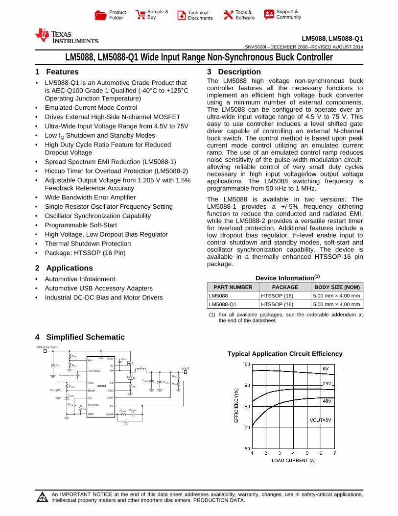
Product
Folder
Sample &Buy
Technical
Documents
Tools &
Software
Support &Community
LM5088, LM5088-Q1SNVS600I –DECEMBER 2008–REVISED AUGUST 2014
LM5088, LM5088-Q1 Wide Input Range Non-Synchronous Buck Controller1 Features 3 Description
The LM5088 high voltage non-synchronous buck1• LM5088-Q1 is an Automotive Grade Product that
controller features all the necessary functions tois AEC-Q100 Grade 1 Qualified (-40°C to +125°Cimplement an efficient high voltage buck converterOperating Junction Temperature) using a minimum number of external components.
• Emulated Current Mode Control The LM5088 can be configured to operate over anultra-wide input voltage range of 4.5 V to 75 V. This• Drives External High-Side N-channel MOSFETeasy to use controller includes a level shifted gate• Ultra-Wide Input Voltage Range from 4.5V to 75Vdriver capable of controlling an external N-channel
• Low IQ Shutdown and Standby Modes buck switch. The control method is based upon peak• High Duty Cycle Ratio Feature for Reduced current mode control utilizing an emulated current
Dropout Voltage ramp. The use of an emulated control ramp reducesnoise sensitivity of the pulse-width modulation circuit,• Spread Spectrum EMI Reduction (LM5088-1)allowing reliable control of very small duty cycles• Hiccup Timer for Overload Protection (LM5088-2) necessary in high input voltage/low output voltage
• Adjustable Output Voltage from 1.205 V with 1.5% applications. The LM5088 switching frequency isFeedback Reference Accuracy programmable from 50 kHz to 1 MHz.
• Wide Bandwidth Error Amplifier The LM5088 is available in two versions: TheLM5088-1 provides a +/-5% frequency dithering• Single Resistor Oscillator Frequency Settingfunction to reduce the conducted and radiated EMI,• Oscillator Synchronization Capabilitywhile the LM5088-2 provides a versatile restart timer• Programmable Soft-Start for overload protection. Additional features include a
• High Voltage, Low Dropout Bias Regulator low dropout bias regulator, tri-level enable input tocontrol shutdown and standby modes, soft-start and• Thermal Shutdown Protectionoscillator synchronization capability. The device is• Package: HTSSOP (16 Pin) available in a thermally enhanced HTSSOP-16 pinpackage.2 Applications
Device Information(1)• Automotive InfotainmentPART NUMBER PACKAGE BODY SIZE (NOM)• Automotive USB Accessory Adapters
LM5088 HTSSOP (16) 5.00 mm × 4.00 mm• Industrial DC-DC Bias and Motor DriversLM5088-Q1 HTSSOP (16) 5.00 mm × 4.00 mm
(1) For all available packages, see the orderable addendum atthe end of the datasheet.
4 Simplified Schematic
Typical Application Circuit Efficiency
1
An IMPORTANT NOTICE at the end of this data sheet addresses availability, warranty, changes, use in safety-critical applications,intellectual property matters and other important disclaimers. PRODUCTION DATA.
LM5088, LM5088-Q1SNVS600I –DECEMBER 2008–REVISED AUGUST 2014 www.ti.com
Table of Contents8.4 Device Functional Modes........................................ 191 Features .................................................................. 1
9 Application and Implementation ........................ 202 Applications ........................................................... 19.1 Application Information............................................ 203 Description ............................................................. 19.2 Typical Application .................................................. 204 Simplified Schematic............................................. 19.3 Design Requirements.............................................. 205 Revision History..................................................... 29.4 Detailed Design Procedure ..................................... 206 Pin Configuration and Functions ......................... 3
10 Power Supply Recommendations ..................... 297 Specifications......................................................... 510.1 Thermal Considerations ........................................ 297.1 Absolute Maximum Ratings ...................................... 5
11 Layout................................................................... 327.2 Handling Ratings....................................................... 511.1 Layout Guidelines ................................................. 327.3 Recommended Operating Conditions....................... 511.2 Layout Example .................................................... 327.4 Thermal Information .................................................. 5
12 Device and Documentation Support ................. 337.5 Electrical Characteristics........................................... 612.1 Related Links ........................................................ 337.6 Typical Characteristics .............................................. 812.2 Trademarks ........................................................... 338 Detailed Description ............................................ 1012.3 Electrostatic Discharge Caution............................ 338.1 Overview ................................................................. 1012.4 Glossary ................................................................ 338.2 Functional Block Diagram ....................................... 10
13 Mechanical, Packaging, and Orderable8.3 Feature Description................................................. 11Information ........................................................... 33
5 Revision HistoryNOTE: Page numbers for previous revisions may differ from page numbers in the current version.
Changes from Revision H (March 2013) to Revision I Page
• Changed data sheet flow and layout to conform with new TI standards. Added the following sections: DeviceInformation Table, Application and Implementation; Power Supply Recommendations; Layout; Device andDocumentation Support; Mechanical, Packaging, and Ordering Information ........................................................................ 1
• Changed "x" to "-" ................................................................................................................................................................ 13• Added unit "kΩ" .................................................................................................................................................................... 20• Deleted "/A" in the numerator of Equation 11 ..................................................................................................................... 22
Changes from Revision G (March 2013) to Revision H Page
• Changed layout of data sheet from National to TI format ..................................................................................................... 1
2 Submit Documentation Feedback Copyright © 2008–2014, Texas Instruments Incorporated
Product Folder Links: LM5088 LM5088-Q1

VIN
EN
SS
RAMP
RT
GND
COMP
VCC
BOOT
HG
SW
CS
CSG
FB OUT
RES
EP
HTSSOP-16
VIN
EN
SS
RAMP
RT
GND
COMP
VCC
BOOT
HG
SW
CS
CSG
FB OUT
DITH
EP
HTSSOP-16
LM5088, LM5088-Q1www.ti.com SNVS600I –DECEMBER 2008–REVISED AUGUST 2014
6 Pin Configuration and Functions
16-Pin (Dither Version)PWP Package
Top View
16-Pin (Restart Version)PWP Package
Top View
Copyright © 2008–2014, Texas Instruments Incorporated Submit Documentation Feedback 3
Product Folder Links: LM5088 LM5088-Q1
LM5088, LM5088-Q1SNVS600I –DECEMBER 2008–REVISED AUGUST 2014 www.ti.com
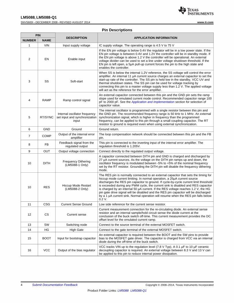
Pin DescriptionsPIN
DESCRIPTION APPLICATION INFORMATIONNUMBER NAME
1 VIN Input supply voltage IC supply voltage. The operating range is 4.5 V to 75 VIf the EN pin voltage is below 0.4V the regulator will be in a low power state. If theEN pin voltage is between 0.4V and 1.2V the controller will be in standby mode. Ifthe EN pin voltage is above 1.2 V the controller will be operational. An external2 EN Enable input voltage divider can be used to set a line under voltage shutdown threshold. If theEN pin is left open, a 5µA pull-up current forces the pin to the high state andenables the controller.When SS is below the internal 1.2V reference, the SS voltage will control the erroramplifier. An internal 11 µA current source charges an external capacitor to set thestart-up rate of the controller. The SS pin is held low in the standby, VCC UV and3 SS Soft-start thermal shutdown states. The SS pin can be used for voltage tracking byconnecting this pin to a master voltage supply less than 1.2 V. The applied voltagewill act as the reference for the error amplifier.An external capacitor connected between this pin and the GND pin sets the rampslope used for emulated current mode control. Recommended capacitor range 1004 RAMP Ramp control signal pF to 2000 pF. See the Application and Implementation section for selection ofcapacitor value.The internal oscillator is programmed with a single resistor between this pin and
Internal oscillator frequency the GND pin. The recommended frequency range is 50 kHz to 1 MHz. An external5 RT/SYNC set input and synchronization synchronization signal, which is higher in frequency than the programmed
input frequency, can be applied to this pin through a small coupling capacitor. The RTresistor to ground is required even when using external synchronization.
6 GND Ground Ground return.Output of the internal error The loop compensation network should be connected between this pin and the FB7 COMP amplifier pin.Feedback signal from the This pin is connected to the inverting input of the internal error amplifier. The8 FB regulated output regulation threshold is 1.205V.
9 OUT Output voltage connection Connect directly to the regulated output voltage.A capacitor connected between DITH pin and GND is charged and discharged by27 µA current sources. As the voltage on the DITH pin ramps up and down, theFrequency Dithering10 DITH oscillator frequency is modulated between -5% to +5% of the nominal frequency(LM5088-1 Only) set by the RT resistor. Grounding the DITH pin will disable the frequency ditheringmode.The RES pin is normally connected to an external capacitor that sets the timing forhiccup mode current limiting. In normal operation, a 25µA current sourcedischarges the RES pin capacitor to ground. If cycle-by-cycle current limit threshold
Hiccup Mode Restart is exceeded during any PWM cycle, the current sink is disabled and RES capacitor10 RES (LM5088-2 Only) is charged by an internal 50 µA current. If the RES voltage reaches 1.2 V, the HGpin gate drive signal will be disabled and the RES pin capacitor will be dischargedby a 1 µA current sink. Normal operation will resume when the RES pin falls below0.2 V.
11 CSG Current Sense Ground Low side reference for the current sense resistor.Current measurement connection for the re-circulating diode. An external senseresistor and an internal sample/hold circuit sense the diode current at the12 CS Current sense conclusion of the buck switch off-time. This current measurement provides the DCoffset level for the emulated current ramp.
13 SW Switching node Connect to the source terminal of the external MOSFET switch.14 HG High Gate Connect to the gate terminal of the external MOSFET switch.
An external capacitor is required between the BOOT and the SW pins to provide15 BOOT Input for bootstrap capacitor bias to the MOSFET gate driver. The capacitor is charged from VCC via an internal
diode during the off-time of the buck switch.VCC tracks VIN up to the regulation level (7.8 V Typ). A 0.1 µF to 10 µF ceramic
16 VCC Output of the bias regulator decoupling capacitor is required. An external voltage between 8.3 V and 13 V canbe applied to this pin to reduce internal power dissipation.
4 Submit Documentation Feedback Copyright © 2008–2014, Texas Instruments Incorporated
Product Folder Links: LM5088 LM5088-Q1
LM5088, LM5088-Q1www.ti.com SNVS600I –DECEMBER 2008–REVISED AUGUST 2014
7 Specifications
7.1 Absolute Maximum Ratings (1) (2)
over operating free-air temperature range (unless otherwise noted)MIN MAX UNIT
VIN, VOUT to GND 76 VBOOT to GND 90 VSW to GND –2 76 VVCC to GND –0.3 16 VHG to SW –0.3 BOOT+0.3 VEN to GND 14 VBOOT to SW –0.3 16 VCS, CSG to GND –0.3 0.3 VAll other inputs to GND –0.3 7 VJunction Temperature + 150 °C
(1) Absolute Maximum Ratings are limits beyond which damage to the device may occur.(2) If Military/Aerospace specified devices are required, please contact the Texas Instruments Sales Office/ Distributors for availability and
specifications.
7.2 Handling RatingsMIN MAX UNIT
Tstg Storage temperature range –65 + 150 °CHuman body model (HBM), per ANSI/ESDA/JEDEC JS-001, all 2V(ESD) Electrostatic discharge kVpins (1) (2)
(1) JEDEC document JEP155 states that 500-V HBM allows safe manufacturing with a standard ESD control process.(2) The human body model is a 100 pF capacitor discharged through a 1.5 kΩ resistor into each pin.
7.3 Recommended Operating Conditions (1)
over operating free-air temperature range (unless otherwise noted)MIN MAX UNIT
VIN Voltage 4.5 75 VVCC Voltage (externally supplied) 8.3 13 VOperation Junction Temperature –40 +125 °C
(1) Operating Ratings are conditions under which operation of the device is intended to be functional. For specified performance limits andassociated test conditions, see the Electrical Characteristics.
7.4 Thermal InformationLM5088(Q1)
THERMAL METRIC (1) PWP UNIT16 PINS
RθJA Junction-to-ambient thermal resistance 40°C/W
RθJC(bot) Junction-to-case (bottom) thermal resistance 6
(1) For more information about traditional and new thermal metrics, see the IC Package Thermal Metrics application report, SPRA953.
Copyright © 2008–2014, Texas Instruments Incorporated Submit Documentation Feedback 5
Product Folder Links: LM5088 LM5088-Q1
LM5088, LM5088-Q1SNVS600I –DECEMBER 2008–REVISED AUGUST 2014 www.ti.com
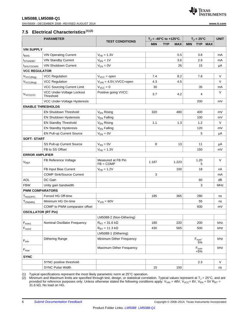
7.5 Electrical Characteristics (1) (2)
PARAMETER TJ = -40°C to +125°C. TJ = 25°C UNITTEST CONDITIONS
MIN TYP MAX MIN TYP MAXVIN SUPPLYIBIAS VIN Operating Current VFB = 1.3V 5.5 3.8 mAISTANDBY VIN Standby Current VEN = 1V 3.6 2.9 mAISHUTDOWN VIN Shutdown Current VEN = 0V 26 15 µAVCC REGULATORVVCC(Reg) VCC Regulation VVCC = open 7.4 8.2 7.8 VVVCC(Reg) VCC Regulation VVIN = 4.5V,VVCC=open 4.3 4.5 V
VCC Sourcing Current Limit VVCC = 0 30 35 mAVCC Under-Voltage Lockout Positive going VVCC VVVCC(UV) 3.7 4.2 4ThresholdVCC Under-Voltage Hysteresis 200 mV
ENABLE THRESHOLDSEN Shutdown Threshold VEN Rising 320 480 400 mVEN Shutdown Hysteresis VEN Falling 100 mVEN Standby Threshold VEN Rising 1.1 1.3 1.2 VEN Standby Hysteresis VEN Falling 120 mVEN Pull-up Current Source VEN = 0V 5 µA
SOFT- STARTSS Pull-up Current Source VSS = 0V 8 13 11 µAFB to SS Offset VFB = 1.3V 150 mV
ERROR AMPLIFIERFB Reference Voltage Measured at FB Pin 1.20 VVREF 1.187 1.223FB = COMP 5FB Input Bias Current VFB = 1.2V 100 18 nACOMP Sink/Source Current 3 mA
AOL DC Gain 60 dBFBW Unity gain bandwidth 3 MHzPWM COMPARATORSTHG(OFF) Forced HG Off-time 185 365 280 nsTON(MIN) Minimum HG On-time VVIN = 60V 55 ns
COMP to PWM comparator offset 930 mVOSCILLATOR (RT Pin)
LM5088-2 (Non-Dithering)Fnom1 Nominal Oscillator Frequency RRT = 31.6 kΩ 180 220 200 kHzFnom2 RRT = 11.3 kΩ 430 565 500 kHz
LM5088-1 (Dithering)Dithering Range Minimum Dither Frequency Fnom- kHzFmin 5%
Maximum Dither Frequency Fnom kHzFmax +5%SYNC
SYNC positive threshold 2.3 VSYNC Pulse Width 15 150 ns
(1) Typical specifications represent the most likely parametric norm at 25°C operation.(2) Minimum and Maximum limits are specified through test, design, or statistical correlation. Typical values represent at TJ = 25°C, and are
provided for reference purposes only. Unless otherwise stated the following conditions apply: VVIN = 48V, VVCC= 8V, VEN = 5V RRT =31.6 kΩ, No load on HG.
6 Submit Documentation Feedback Copyright © 2008–2014, Texas Instruments Incorporated
Product Folder Links: LM5088 LM5088-Q1
LM5088, LM5088-Q1www.ti.com SNVS600I –DECEMBER 2008–REVISED AUGUST 2014
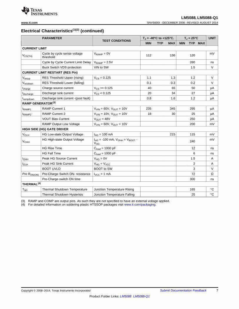
Electrical Characteristics(1)(2) (continued)PARAMETER TJ = -40°C to +125°C. TJ = 25°C UNIT
TEST CONDITIONSMIN TYP MAX MIN TYP MAX
CURRENT LIMITCycle by cycle sense voltage VRAMP = 0V mVVCS(TH) 112 136 120thresholdCycle by Cycle Current Limit Delay VRAMP = 2.5V 280 nsBuck Switch VDS protection VIN to SW 1.5 V
CURRENT LIMIT RESTART (RES Pin)Vresup RES Threshold Upper (rising) VCS = 0.125 1.1 1.3 1.2 VVresdown RES Threshold Lower (falling) 0.1 0.3 0.2 VIcharge Charge source current VCS >= 0.125 40 65 50 µAIdischarge Discharge sink current VCS < 0.125 20 34 27 µAIrampdown Discharge sink current -(post fault) 0.8 1.6 1.2 µARAMP GENERATOR (3)
IRAMP1 RAMP Current 1 VVIN = 60V, VOUT = 10V 235 345 295 µAIRAMP2 RAMP Current 2 VVIN = 10V, VOUT = 10V 18 30 25 µA
VOUT Bias Current VOUT = 48V 250 µARAMP Output Low Voltage VVIN = 60V, VOUT = 10V 200 mV
HIGH SIDE (HG) GATE DRIVERVOLH HG Low-state Output Voltage IHG = 100 mA 215 115 mV
HG High-state Output Voltage IHG = -100 mA, VOHH = VBOOT - mVVOHH 240VHG
HG Rise Time Cload = 1000 pF 12 nsHG Fall Time Cload = 1000 pF 6 ns
IOHH Peak HG Source Current VHG = 0V 1.5 AIOLH Peak HG Sink Current VHG = VVCC 2 A
BOOT UVLO BOOT to SW 3 VPre RDS(ON) Pre-Charge Switch ON- resistance IVCC = 1 mA 72 Ω
Pre-Charge switch ON time 300 nsTHERMAL (4)
TSD Thermal Shutdown Temperature Junction Temperature Rising 165 °CThermal Shutdown Hysterisis Junction Temperature Falling 25 °C
(3) RAMP and COMP are output pins. As such they are not specified to have an external voltage applied.(4) For detailed information on soldering plastic HTSSOP packages visit www.ti.com/packaging.
Copyright © 2008–2014, Texas Instruments Incorporated Submit Documentation Feedback 7
Product Folder Links: LM5088 LM5088-Q1
LM5088, LM5088-Q1SNVS600I –DECEMBER 2008–REVISED AUGUST 2014 www.ti.com
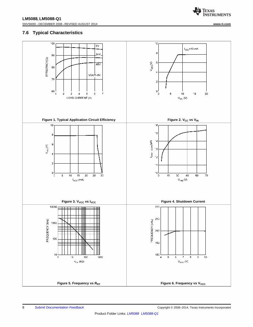
7.6 Typical Characteristics
Figure 1. Typical Application Circuit Efficiency Figure 2. VCC vs VIN
Figure 3. VVCC vs IVCC Figure 4. Shutdown Current
Figure 5. Frequency vs RRT Figure 6. Frequency vs VVCC
8 Submit Documentation Feedback Copyright © 2008–2014, Texas Instruments Incorporated
Product Folder Links: LM5088 LM5088-Q1

1E+04 1E+05 1E+06 1E+07
FREQUENCY (Hz)
-10
50
GA
IN (
dB)
0
10
20
30
40
-30
150
0
30
60
90
120P
HA
SE
(°)
LM5088, LM5088-Q1www.ti.com SNVS600I –DECEMBER 2008–REVISED AUGUST 2014
Typical Characteristics (continued)
Figure 7. VFB vs Temperature Figure 8. Forced-Off Time vs Temperature
Figure 9. Soft-Start vs Temperature Figure 10. Current-Limit vs Temperature
Figure 11. Frequency vs Temperature Figure 12. Error Amplifier Gain/Phase
Copyright © 2008–2014, Texas Instruments Incorporated Submit Documentation Feedback 9
Product Folder Links: LM5088 LM5088-Q1
FB
VIN VCC
SW
RT
Regulator
DRIVER
BOOT
LEVELSHIFT
THERMALSHUTDOWN
UVLO
ERRORAMP
DIS
COMP
TRACKSAMPLE
andHOLD
CLKGND
CLK
CSG
CS
CLK
RAMP GENERATOR
+
SHUTDOWN
PWM
I- LIMIT
OUT
RAMP
SS
VIN
STANDBY5 uA
1.2
VIN
EN
Ir
HG
CLK
S
R
Q
Q
CLK
FREQUENCYDITHERING
STANDBY
SYNC
DITHERLM5088 -1 ONLY
OSCILLATOR
HICCUPRESTART
LOGIC
Rs
RFB1
DITHER
RES
RFB2
QL
D
VOUT
CBOOT
LM5088
UVLO
MINIMUM OFF-TIME
LOGIC
7.7V
HICCUP RESTARTLM5088 - 2 ONLY
5V
A = -10
CRES/DITH
CSYNC
1.2VRUV2
RUV1CFT
CIN
4.5V-75V
CSS
CHF
RCOMP
CCOMP
RRT CRAMP
COUT
0.9V
0.4V
5V
11 uA
CVCC
1.205V
LM5088, LM5088-Q1SNVS600I –DECEMBER 2008–REVISED AUGUST 2014 www.ti.com
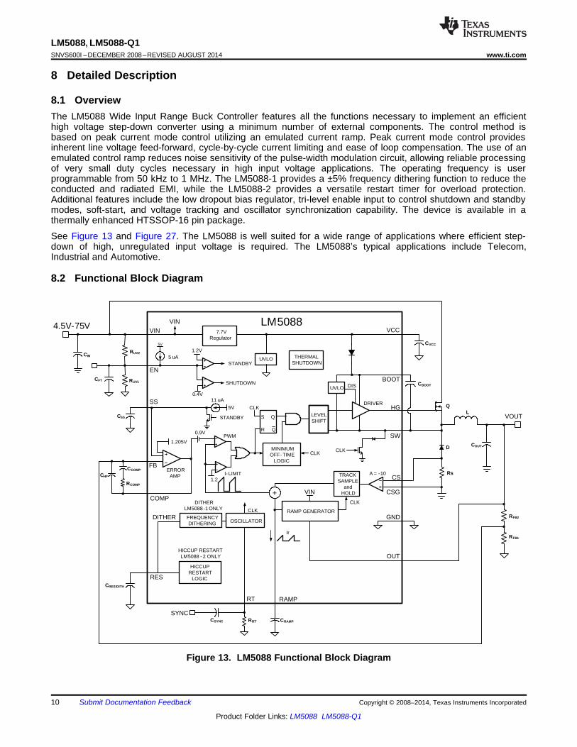
8 Detailed Description
8.1 OverviewThe LM5088 Wide Input Range Buck Controller features all the functions necessary to implement an efficienthigh voltage step-down converter using a minimum number of external components. The control method isbased on peak current mode control utilizing an emulated current ramp. Peak current mode control providesinherent line voltage feed-forward, cycle-by-cycle current limiting and ease of loop compensation. The use of anemulated control ramp reduces noise sensitivity of the pulse-width modulation circuit, allowing reliable processingof very small duty cycles necessary in high input voltage applications. The operating frequency is userprogrammable from 50 kHz to 1 MHz. The LM5088-1 provides a ±5% frequency dithering function to reduce theconducted and radiated EMI, while the LM5088-2 provides a versatile restart timer for overload protection.Additional features include the low dropout bias regulator, tri-level enable input to control shutdown and standbymodes, soft-start, and voltage tracking and oscillator synchronization capability. The device is available in athermally enhanced HTSSOP-16 pin package.
See Figure 13 and Figure 27. The LM5088 is well suited for a wide range of applications where efficient step-down of high, unregulated input voltage is required. The LM5088’s typical applications include Telecom,Industrial and Automotive.
8.2 Functional Block Diagram
Figure 13. LM5088 Functional Block Diagram
10 Submit Documentation Feedback Copyright © 2008–2014, Texas Instruments Incorporated
Product Folder Links: LM5088 LM5088-Q1
RRT =152 pF
1fSW
- 280 ns
LM5088, LM5088-Q1www.ti.com SNVS600I –DECEMBER 2008–REVISED AUGUST 2014
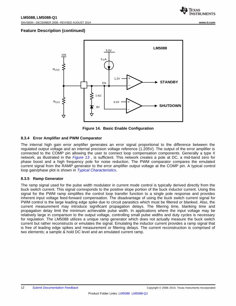
8.3 Feature Description
8.3.1 High Voltage Low-Dropout RegulatorThe LM5088 contains a high voltage, low-dropout regulator that provides the VCC bias supply for the controllerand the bootstrap MOSFET gate driver. The input pin (VIN) can be connected directly to an input voltage as highas 75V. The output of the VCC regulator (7.8V) is internally current limited to 30 mA. Upon power up, theregulator sources current into the capacitor connected to the VCC pin. When the voltage at the VCC pin exceedsthe upper VCC UV threshold of 4.0V and the EN pin is greater than 1.2 Volts, the output (HG) is enabled and asoft-start sequence begins. The output is terminated if VCC falls below its lower UV threshold (3.8V) or the ENpin falls below 1.1V. When VIN is less than VCC regulation point of 7.8V, then the internal pass device acts as aswitch. Thereby, VCC tracks VIN with a voltage drop determined by the RDS(ON) of the internal switch andoperating current of the controller. The required VCC capacitor value is dependant on system startupcharacteristics with a minimum value no less than 0.1 µF.
An auxiliary supply voltage can be applied to the VCC pin to reduce the IC power dissipation. If the auxiliaryvoltage is greater than 8.2V, the internal regulator will be disabled. The VCC regulator series pass transistorincludes a diode between VCC and VIN that should not be forward biased in normal operation.
In high voltage applications, additional care should be taken to ensure that the VIN pin does not exceed theabsolute maximum voltage rating of 76V. During line or load transients, voltage ringing on the VIN pin thatexceeds the absolute maximum ratings may damage the IC. Both careful PC board layout and the use of highquality bypass capacitors located close to the VIN and GND pins are essential.
8.3.2 Line Under-Voltage DetectorThe LM5088 contains a dual level under-voltage lockout (UVLO) circuit. When the EN pin is below 0.4V, thecontroller is in a low current shutdown mode. When the EN pin is greater than 0.4V but less than 1.2V, thecontroller is in a standby mode. In standby mode the VCC regulator is active but the output switch is disabledand the SS pin is held low. When the EN pin exceeds 1.2V and VCC exceeds the VCC UV threshold, the SS pinand the output switch is enabled and normal operation begins. An internal 5 µA pull-up current source at the ENpin configures the controller to be fully operational if the EN pin is left open.
An external VIN UVLO set-point voltage divider from VIN to GND can be used to set the minimum startup inputvoltage of the controller. The divider must be designed such that the voltage at the EN pin exceeds 1.2V (typ)when VIN is in the desired operating range. The internal 5 µA pull-up current source must be included incalculations of the external set-point divider. 100 mV of hysteresis is included for both the shutdown and standbythresholds. The EN pin is internally connected to a 1 kΩ resistor and an 8V zener clamp. If the voltage at the ENpin exceeds 8V, the bias current for the EN pin will increase at the rate of 1mA/V. The voltage at the EN pinshould never exceed 14V.
8.3.3 Oscillator and Sync CapabilityThe LM5088 oscillator frequency is set by a single external resistor connected between the RT pin and the GNDpin. The RT resistor should be located very close to the device. To set a desired oscillator frequency (fSW), thenecessary value of RT resistor can be calculated from the following equation:
(1)
The RT pin can also be used to synchronize the internal oscillator to an external clock. The internal oscillator issynchronized to an external clock by AC coupling a positive edge into the RT/SYNC pin. The RT/SYNC pinvoltage must exceed 3V to trip the internal clock synchronization pulse detector. The free-running frequencyshould be set nominally 15% below the external clock frequency and the pulse width applied to the RT/SYNC pinmust be less than 150ns. Synchronization to an external clock more than twice the free-running frequency canproduce abnormal behavior of the pulse-width modulator.
Copyright © 2008–2014, Texas Instruments Incorporated Submit Documentation Feedback 11
Product Folder Links: LM5088 LM5088-Q1
1.2VSTANDBY
0.4VSHUTDOWN
VIN
5.0V
EN
RUV1
5 PA
LM5088
RUV2
1 k:
8V
LM5088, LM5088-Q1SNVS600I –DECEMBER 2008–REVISED AUGUST 2014 www.ti.com
Feature Description (continued)
Figure 14. Basic Enable Configuration
8.3.4 Error Amplifier and PWM ComparatorThe internal high gain error amplifier generates an error signal proportional to the difference between theregulated output voltage and an internal precision voltage reference (1.205V). The output of the error amplifier isconnected to the COMP pin allowing the user to connect loop compensation components. Generally a type IInetwork, as illustrated in the Figure 13 , is sufficient. This network creates a pole at DC, a mid-band zero forphase boost and a high frequency pole for noise reduction. The PWM comparator compares the emulatedcurrent signal from the RAMP generator to the error amplifier output voltage at the COMP pin. A typical controlloop gain/phase plot is shown in Typical Characteristics.
8.3.5 Ramp GeneratorThe ramp signal used for the pulse width modulator in current mode control is typically derived directly from thebuck switch current. This signal corresponds to the positive slope portion of the buck inductor current. Using thissignal for the PWM ramp simplifies the control loop transfer function to a single pole response and providesinherent input voltage feed-forward compensation. The disadvantage of using the buck switch current signal forPWM control is the large leading edge spike due to circuit parasitics which must be filtered or blanked. Also, thecurrent measurement may introduce significant propagation delays. The filtering time, blanking time andpropagation delay limit the minimum achievable pulse width. In applications where the input voltage may berelatively large in comparison to the output voltage, controlling small pulse widths and duty cycles is necessaryfor regulation. The LM5088 utilizes a unique ramp generator which does not actually measure the buck switchcurrent but rather reconstructs or emulates the signal. Emulating the inductor current provides a ramp signal thatis free of leading edge spikes and measurement or filtering delays. The current reconstruction is comprised oftwo elements; a sample & hold DC level and an emulated current ramp.
12 Submit Documentation Feedback Copyright © 2008–2014, Texas Instruments Incorporated
Product Folder Links: LM5088 LM5088-Q1
CRAMP =RS x A
gm x L
TON
Sample and Hold DC Level V/A10 x RS
RAMP TON(5 PA/V x (VIN ± VOUT) + 25 PA) x
CRAMP
LM5088, LM5088-Q1www.ti.com SNVS600I –DECEMBER 2008–REVISED AUGUST 2014
Feature Description (continued)
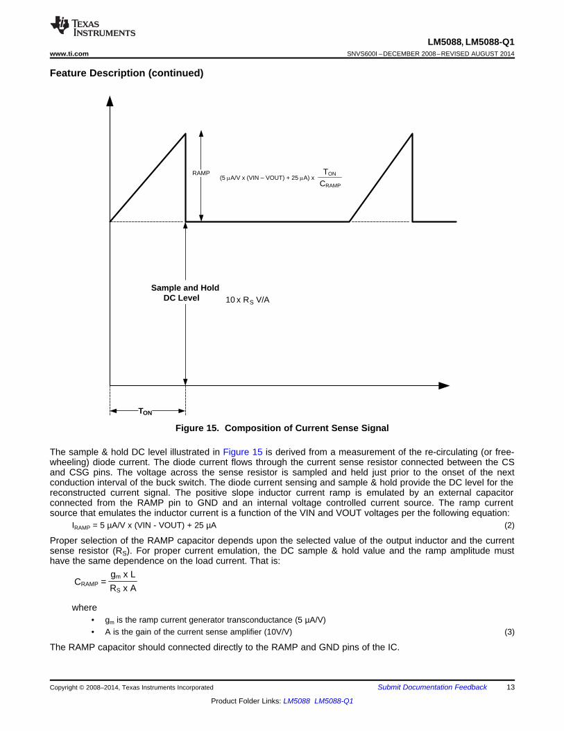
Figure 15. Composition of Current Sense Signal
The sample & hold DC level illustrated in Figure 15 is derived from a measurement of the re-circulating (or free-wheeling) diode current. The diode current flows through the current sense resistor connected between the CSand CSG pins. The voltage across the sense resistor is sampled and held just prior to the onset of the nextconduction interval of the buck switch. The diode current sensing and sample & hold provide the DC level for thereconstructed current signal. The positive slope inductor current ramp is emulated by an external capacitorconnected from the RAMP pin to GND and an internal voltage controlled current source. The ramp currentsource that emulates the inductor current is a function of the VIN and VOUT voltages per the following equation:
IRAMP = 5 µA/V x (VIN - VOUT) + 25 µA (2)
Proper selection of the RAMP capacitor depends upon the selected value of the output inductor and the currentsense resistor (RS). For proper current emulation, the DC sample & hold value and the ramp amplitude musthave the same dependence on the load current. That is:
where• gm is the ramp current generator transconductance (5 µA/V)• A is the gain of the current sense amplifier (10V/V) (3)
The RAMP capacitor should connected directly to the RAMP and GND pins of the IC.
Copyright © 2008–2014, Texas Instruments Incorporated Submit Documentation Feedback 13
Product Folder Links: LM5088 LM5088-Q1
Dropout_Voltage = VOUT xTOSC - TOFF(max)
TOFF(max)
LM5088, LM5088-Q1SNVS600I –DECEMBER 2008–REVISED AUGUST 2014 www.ti.com
Feature Description (continued)For duty cycles greater than 50%, peak current mode control circuits are subject to sub-harmonic oscillation.Sub-harmonic oscillation is normally characterized by alternating wide and narrow pulses at the SW pin. Addinga fixed slope voltage ramp (slope compensation) to the current sense signal prevents this oscillation. The 25 µAoffset current supplied by the emulated current source provides a fixed slope to the ramp signal. In some highoutput voltage, high duty cycles applications; additional slope compensation may be required. In theseapplications, a pull-up resistor may be added between the RAMP and VCC pins to increase the ramp slopecompensation. A formula to configure pull-up resistor is shown in Application and Implementation.
8.3.6 Dropout Voltage ReductionThe LM5088 features unique circuitry to reduce the dropout voltage. Dropout voltage is defined as the differencebetween the minimum input voltage to maintain regulation and the output voltage (VINmin - Vout). Dropout voltagethus determines the lowest input voltage at which the converter maintains regulation. In a buck converter,dropout voltage primarily depends upon the maximum duty cycle. The maximum duty cycle is dependant on theoscillator frequency and minimum off-time.
An approximation for the dropout voltage is:
where• TOSC = 1/fSW
• TOFF (max) is the forced off-time (280 ns typical, 365 ns maximum)• fSW is the oscillator frequency• TOSC is the oscillator period (4)
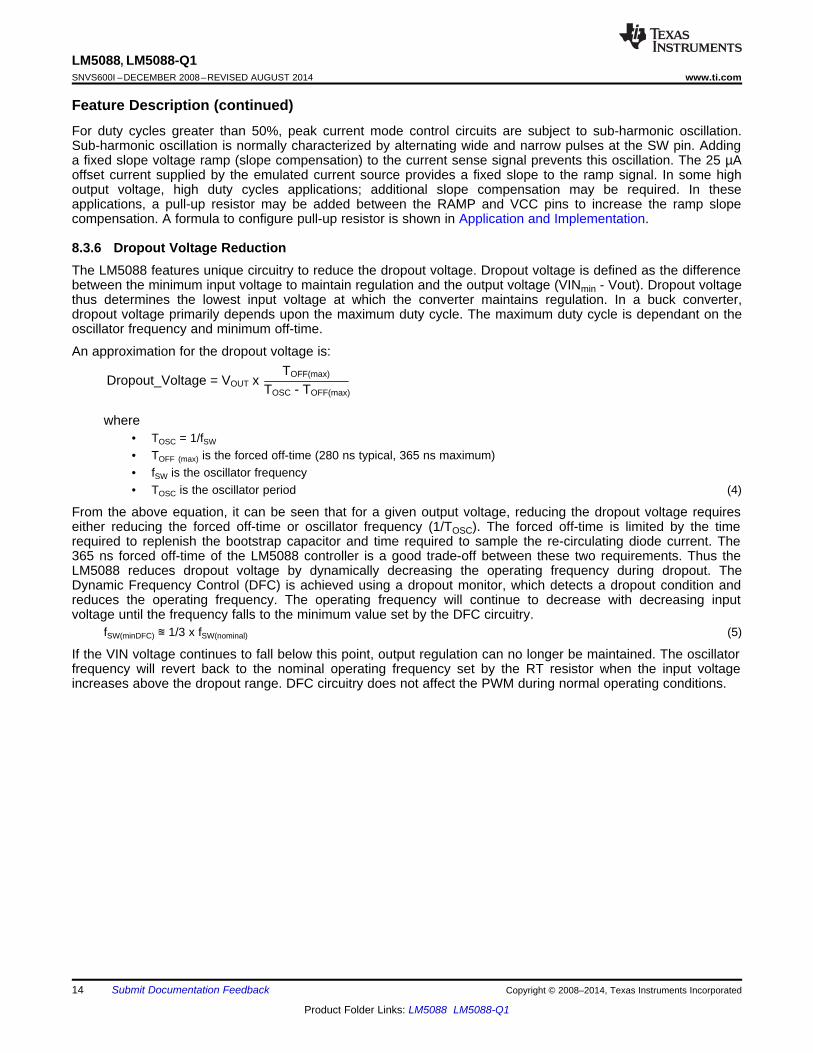
From the above equation, it can be seen that for a given output voltage, reducing the dropout voltage requireseither reducing the forced off-time or oscillator frequency (1/TOSC). The forced off-time is limited by the timerequired to replenish the bootstrap capacitor and time required to sample the re-circulating diode current. The365 ns forced off-time of the LM5088 controller is a good trade-off between these two requirements. Thus theLM5088 reduces dropout voltage by dynamically decreasing the operating frequency during dropout. TheDynamic Frequency Control (DFC) is achieved using a dropout monitor, which detects a dropout condition andreduces the operating frequency. The operating frequency will continue to decrease with decreasing inputvoltage until the frequency falls to the minimum value set by the DFC circuitry.
fSW(minDFC) ≊ 1/3 x fSW(nominal) (5)
If the VIN voltage continues to fall below this point, output regulation can no longer be maintained. The oscillatorfrequency will revert back to the nominal operating frequency set by the RT resistor when the input voltageincreases above the dropout range. DFC circuitry does not affect the PWM during normal operating conditions.
14 Submit Documentation Feedback Copyright © 2008–2014, Texas Instruments Incorporated
Product Folder Links: LM5088 LM5088-Q1
Cdither tfSW x 0.12V100 x 25 PA
Normal Operation Transition Region Low Dropout Mode
E
Dropout
reduce dropout
Forcedoff-time
Forcedoff-time
RegulationPoint
ON
-TIM
CL
KV
OU
TV
IN
fSW(minDFC)
ExtendedTON(max)
TON(max) TON(maxDFC)
increased to
LM5088, LM5088-Q1www.ti.com SNVS600I –DECEMBER 2008–REVISED AUGUST 2014
Feature Description (continued)
Figure 16. Dropout Voltage Reduction using Dynamic Frequency Control
8.3.7 Frequency Dithering (LM5088-1 Only)Electro-Magnetic Interference (EMI) emissions are fundamentally associated with switch-mode power suppliesdue to sharp voltage transitions, diode reverse recovery currents and the ringing of parasitic L-C circuits. Theseemissions will conduct back to the power source or radiate into the environment and potentially interfering withnearby electronic systems. System designers typically use a combination of shielding, filtering and layouttechniques to reduce the EMI emissions sufficiently to satisfy EMI emission standards established by regulatorybodies. In a typical fixed frequency switching converter, narrowband emissions typically peak at the switchingfrequency with the successive harmonics having less energy. Dithering the oscillator frequency spreads the EMIenergy over a range of frequencies, thus reducing the peak levels. Dithering can also reduce the system cost byreducing the size and quantity of EMI filtering components.
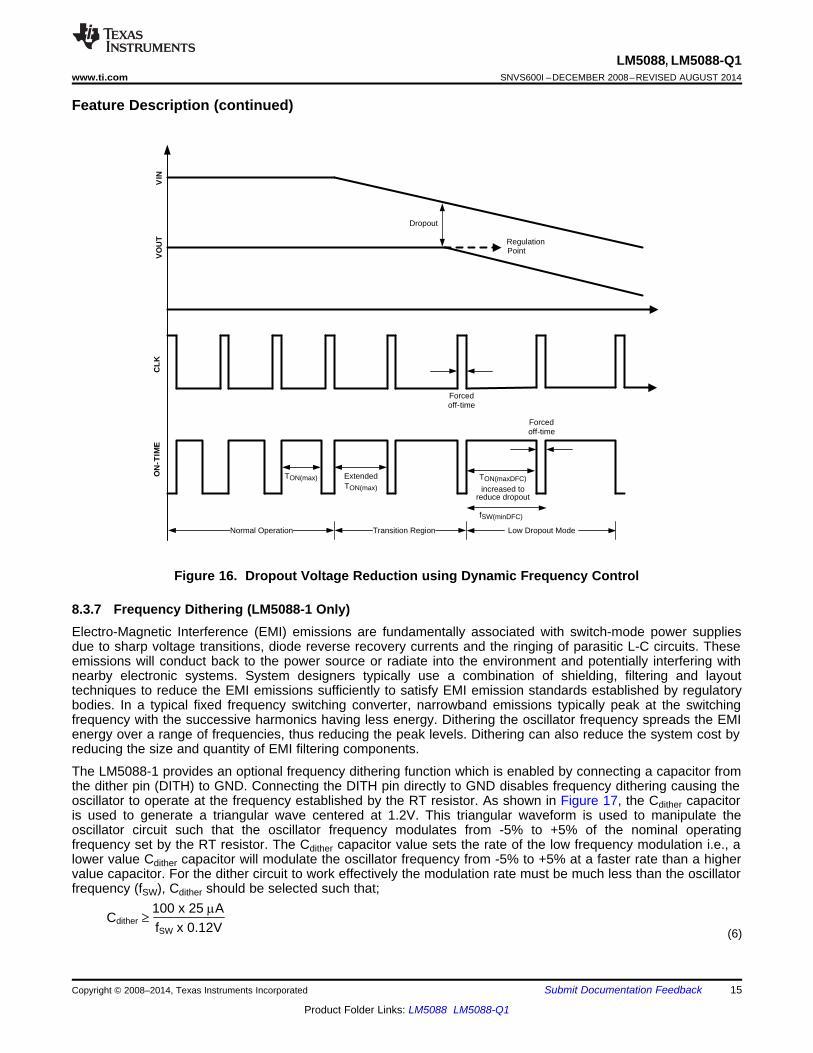
The LM5088-1 provides an optional frequency dithering function which is enabled by connecting a capacitor fromthe dither pin (DITH) to GND. Connecting the DITH pin directly to GND disables frequency dithering causing theoscillator to operate at the frequency established by the RT resistor. As shown in Figure 17, the Cdither capacitoris used to generate a triangular wave centered at 1.2V. This triangular waveform is used to manipulate theoscillator circuit such that the oscillator frequency modulates from -5% to +5% of the nominal operatingfrequency set by the RT resistor. The Cdither capacitor value sets the rate of the low frequency modulation i.e., alower value Cdither capacitor will modulate the oscillator frequency from -5% to +5% at a faster rate than a highervalue capacitor. For the dither circuit to work effectively the modulation rate must be much less than the oscillatorfrequency (fSW), Cdither should be selected such that;
(6)
Copyright © 2008–2014, Texas Instruments Incorporated Submit Documentation Feedback 15
Product Folder Links: LM5088 LM5088-Q1
DITHER
+-
Q
Q
R
S
+-
OscillatorTosc +'tToscTosc -'t
1.26V
Cdither
+5V
25 PA
1.14V1.26V
1.20V
1.14V
LM5088
50 PA
LM5088, LM5088-Q1SNVS600I –DECEMBER 2008–REVISED AUGUST 2014 www.ti.com
Feature Description (continued)
Figure 17. Frequency Dithering Scheme
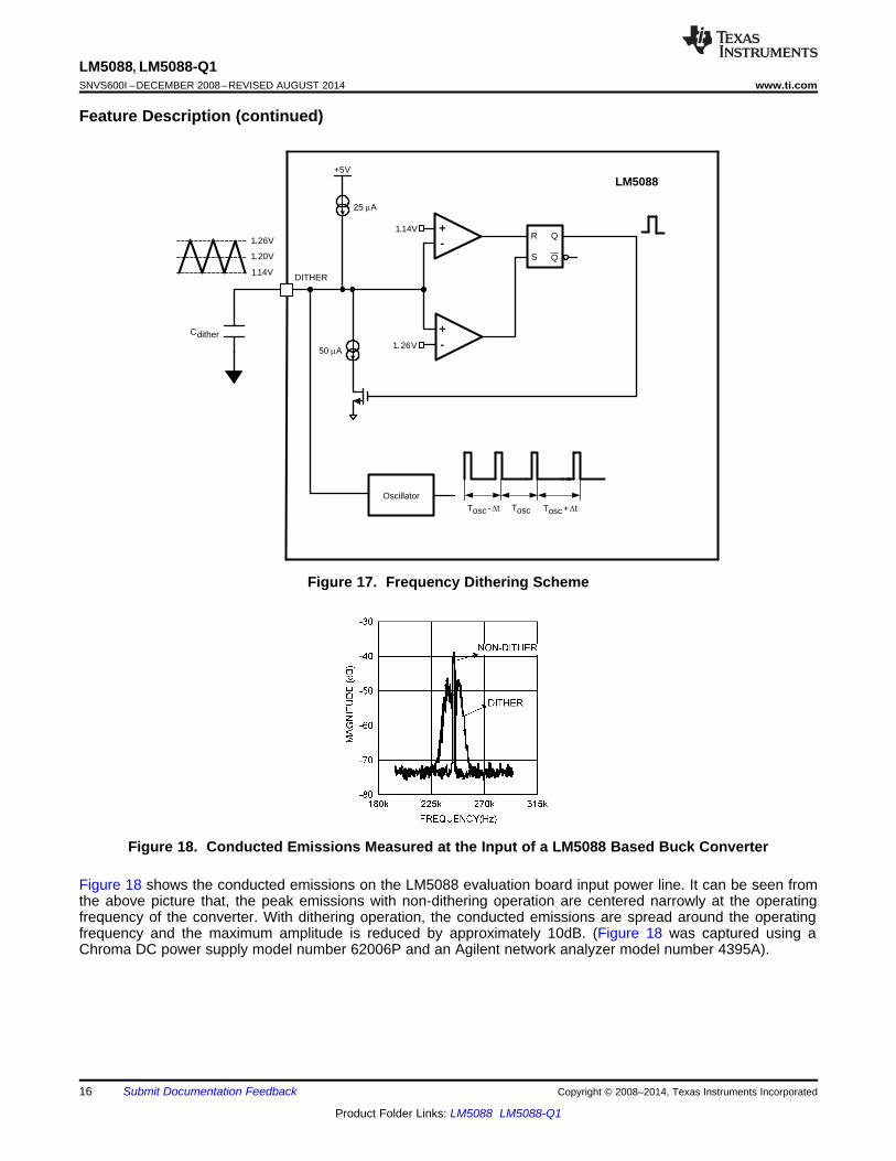
Figure 18. Conducted Emissions Measured at the Input of a LM5088 Based Buck Converter
Figure 18 shows the conducted emissions on the LM5088 evaluation board input power line. It can be seen fromthe above picture that, the peak emissions with non-dithering operation are centered narrowly at the operatingfrequency of the converter. With dithering operation, the conducted emissions are spread around the operatingfrequency and the maximum amplitude is reduced by approximately 10dB. (Figure 18 was captured using aChroma DC power supply model number 62006P and an Agilent network analyzer model number 4395A).
16 Submit Documentation Feedback Copyright © 2008–2014, Texas Instruments Incorporated
Product Folder Links: LM5088 LM5088-Q1
VOUT
VIN x fSW x CRAMP25 PA x
IPEAK =A x RS
VOUT
VIN x fSW x CRAMP1.2V - 25 PA x
0.12VRS
or IPEAK #
LM5088, LM5088-Q1www.ti.com SNVS600I –DECEMBER 2008–REVISED AUGUST 2014
Feature Description (continued)8.3.8 Cycle-by-Cycle Current LimitThe LM5088 contains a current limit feature that protects the circuit from extended over current conditions. Theemulated current signal is directly proportional to the buck switch current and is applied to the current limitcomparator. If the emulated current exceeds 1.2V, the PWM cycle is terminated. The peak inductor currentrequired to trigger the current limit comparator is given by:
where• A = 10V/V is the current sense amplifier gain• CRAMP is the ramp capacitor• RS is the sense resistor
• is the voltage ramp added for slope compensation• 1.2 V is the reference of the current limit comparator (7)
is the voltage ramp added for slope compensation and 1.2V is the reference of the current limit comparator.
Since the current that charges the RAMP capacitor is proportional to VIN-VOUT, if the output is suddenlyshorted, the VOUT term is zero and the RAMP charging current increases. The increased RAMP chargingcurrent will immediately reduce the PWM duty cycle. The LM5088 also includes a buck switch protectionscheme. A dedicated comparator monitors the drain to source voltage of the buck FET when it is turned ON, ifthe VDS exceeds 1.5V, the comparator turns off the buck FET immediately. This feature will help protect the buckFET in catastrophic conditions such as a sudden saturation of the inductor.
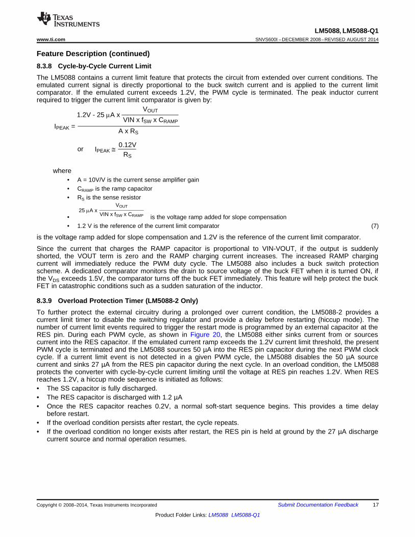
8.3.9 Overload Protection Timer (LM5088-2 Only)To further protect the external circuitry during a prolonged over current condition, the LM5088-2 provides acurrent limit timer to disable the switching regulator and provide a delay before restarting (hiccup mode). Thenumber of current limit events required to trigger the restart mode is programmed by an external capacitor at theRES pin. During each PWM cycle, as shown in Figure 20, the LM5088 either sinks current from or sourcescurrent into the RES capacitor. If the emulated current ramp exceeds the 1.2V current limit threshold, the presentPWM cycle is terminated and the LM5088 sources 50 µA into the RES pin capacitor during the next PWM clockcycle. If a current limit event is not detected in a given PWM cycle, the LM5088 disables the 50 µA sourcecurrent and sinks 27 µA from the RES pin capacitor during the next cycle. In an overload condition, the LM5088protects the converter with cycle-by-cycle current limiting until the voltage at RES pin reaches 1.2V. When RESreaches 1.2V, a hiccup mode sequence is initiated as follows:• The SS capacitor is fully discharged.• The RES capacitor is discharged with 1.2 µA• Once the RES capacitor reaches 0.2V, a normal soft-start sequence begins. This provides a time delay
before restart.• If the overload condition persists after restart, the cycle repeats.• If the overload condition no longer exists after restart, the RES pin is held at ground by the 27 µA discharge
current source and normal operation resumes.
Copyright © 2008–2014, Texas Instruments Incorporated Submit Documentation Feedback 17
Product Folder Links: LM5088 LM5088-Q1
RES
SS
HG
Current Limit Detected at CS
Current Limit PersistentCharge Restart capwith 50 PA current
Discharge Restartcap with 1.2 PA
11PA
0.2V
FB+120 mV
t2t1
1.2V
0V
RES
Hiccupcurrent sourcelogic
Current limit cycle
limit cycle
CLK
+-
LM5088
R
SQ
+-
HG OFF
SS beginsRestart Q
SS = 0
50 PA
5.0V
Non- current
CRESPost-faultDischarge
current
I -Limit
0.2V
1.2V
1.2 PA 27 PA
LM5088, LM5088-Q1SNVS600I –DECEMBER 2008–REVISED AUGUST 2014 www.ti.com
Feature Description (continued)The overload protection timer is very versatile and can be configured for the following modes of protection:1. Cycle-by-Cycle only: The hiccup mode can be completely disabled by connecting the RES pin to GND. In
this configuration, the cycle-by-cycle protection will limit the output current indefinitely and no hiccupsequence will occur.
2. Delayed Hiccup: Connecting a capacitor to the RES pin provides a programmed number of cycle-by-cyclecurrent limit events before initiating a hiccup mode restart, as previously described. The advantage of thisconfiguration is that a short term overload will not cause a hiccup mode restart but during extended overloadconditions, the average dissipation of the power converter will be very low.
3. Externally Controlled Hiccup: The RES pin can also be used as an input. By externally driving the pin to alevel greater than the 1.2V hiccup threshold, the controller will be forced into the delayed restart sequence.For example, the external trigger for a delayed restart sequence could come from an over-temperatureprotection or an output over-voltage sensor.
Figure 19. Current Limit Restart Circuit
Figure 20. Current Limit Restart Timing Diagram
18 Submit Documentation Feedback Copyright © 2008–2014, Texas Instruments Incorporated
Product Folder Links: LM5088 LM5088-Q1
LM5088, LM5088-Q1www.ti.com SNVS600I –DECEMBER 2008–REVISED AUGUST 2014
Feature Description (continued)8.3.10 Soft-StartThe soft-start (SS) feature forces the output to rise linearly until it reaches the steady-state operating voltage setby the feedback resistors. The LM5088 will regulate the FB pin to the SS pin voltage or the internal 1.205Vreference, which ever is lower. At the beginning of the soft-start sequence VSS = 0V and, an internal 11 µAcurrent source gradually increases the voltage of the external soft-start capacitor (CSS). An internal amplifierclamps the SS pin voltage at 120 mV above the FB voltage. This feature provides soft-start controlled recoverywith reduced output overshoot in the event that the output voltage momentarily dips out of regulation.
8.3.11 HG OutputThe LM5088 provides a high current, high-side driver and associated level shift circuit to drive an external N-Channel MOSFET. The gate driver works in conjunction with an internal diode and external bootstrap capacitor.A ceramic bootstrap capacitor is recommended, and should be connected directly between the BOOT and SWpins. During the off-time of the buck switch, the bootstrap capacitor charges from VCC through an internal diode.When operating with a high PWM duty cycle, the HG output will be forced-off each cycle for 365 ns (max) toensure that BOOT capacitor is recharged. A “pre-charge” circuit, comprised of a MOSFET between SW andGND, is turned ON during the forced off-time to help replenish the BOOT capacitor. The pre-charge circuitprovides charge to the BOOT capacitor under light load or pre-biased load conditions when the SW voltage doesnot remain low during the entire off-time.
8.3.12 Thermal ProtectionInternal thermal shutdown circuitry is provided to protect the integrated circuit in the event the maximumoperating temperature is exceeded. When activated, typically at 165°C, the controller is forced into a low powerreset state, disabling the output driver and the bias supply of the controller. The feature prevents catastrophicfailures from accidental device over-heating.
8.4 Device Functional Modes
8.4.1 EN Pin ModesIf the EN pin voltage is below 0.4 V, the regulator will be in a low power state. If the EN pin voltage is between0.4 V and 1.2 V, the controller will be in standby mode. If the EN pin voltage is above 1.2 V, the controller will beoperational. An external voltage divider can be used to set a line under the voltage shutdown threshold. If the ENpin is left open, a 5-μA pull-up current forces the pin to the high state and enables the controller.
Copyright © 2008–2014, Texas Instruments Incorporated Submit Documentation Feedback 19
Product Folder Links: LM5088 LM5088-Q1
RRT =152 pF
250 kHz1 - 280 ns
= 24.5 k:
BOOT
SW
COMP
FB
RAMP
DITH/RES
VCC
VIN
OUT
CS
CSG
VOUT
EN
HG
GND
L
D
Rs
Q
LM5088
CDITHER/RESTART
CIN
CVCC
CSS
CRAMP
RRAMP
RRTRCOMP
CCOMP
CHF
COUT1COUT2
RFB2
RFB1
CBOOT
RUV2
RUV1
VIN (4.5V-75V)
SS
RT/SYNC
LM5088, LM5088-Q1SNVS600I –DECEMBER 2008–REVISED AUGUST 2014 www.ti.com
9 Application and Implementation
9.1 Application InformationThe LM5088 Wide Input Range buck Controller features all the functions necessary to implement an efficienthigh voltage step-down converter using a minimum number of external components. The LM5088 is well suitedfor a wide range of applications where efficient step-down of high, unregulated input voltage is required.
9.2 Typical Application
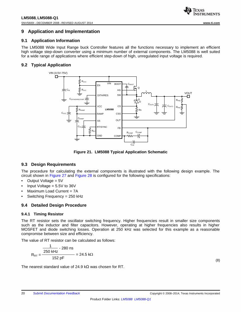
Figure 21. LM5088 Typical Application Schematic
9.3 Design RequirementsThe procedure for calculating the external components is illustrated with the following design example. Thecircuit shown in Figure 27 and Figure 28 is configured for the following specifications:• Output Voltage = 5V• Input Voltage = 5.5V to 36V• Maximum Load Current = 7A• Switching Frequency = 250 kHz
9.4 Detailed Design Procedure
9.4.1 Timing ResistorThe RT resistor sets the oscillator switching frequency. Higher frequencies result in smaller size componentssuch as the inductor and filter capacitors. However, operating at higher frequencies also results in higherMOSFET and diode switching losses. Operation at 250 kHz was selected for this example as a reasonablecompromise between size and efficiency.
The value of RT resistor can be calculated as follows:
(8)
The nearest standard value of 24.9 kΩ was chosen for RT.
20 Submit Documentation Feedback Copyright © 2008–2014, Texas Instruments Incorporated
Product Folder Links: LM5088 LM5088-Q1
L =5V
0.4 x 7A x 250 kHz5V
1 -55V
x = 6.2 PH
0
I PP
T = 1/FSW
IO
L =VOUT
IPP x fSW
VOUT1 -
VIN(max)x
LM5088, LM5088-Q1www.ti.com SNVS600I –DECEMBER 2008–REVISED AUGUST 2014
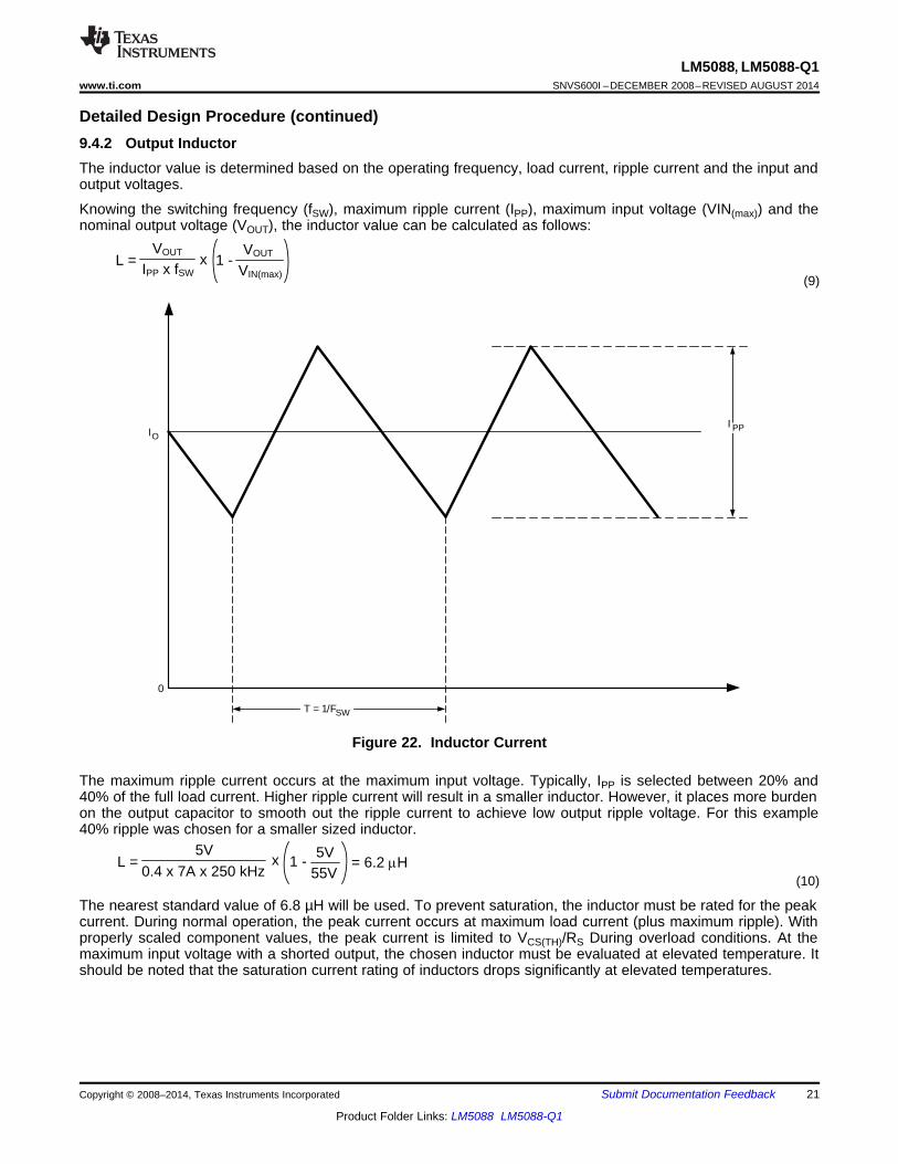
Detailed Design Procedure (continued)9.4.2 Output InductorThe inductor value is determined based on the operating frequency, load current, ripple current and the input andoutput voltages.
Knowing the switching frequency (fSW), maximum ripple current (IPP), maximum input voltage (VIN(max)) and thenominal output voltage (VOUT), the inductor value can be calculated as follows:
(9)
Figure 22. Inductor Current
The maximum ripple current occurs at the maximum input voltage. Typically, IPP is selected between 20% and40% of the full load current. Higher ripple current will result in a smaller inductor. However, it places more burdenon the output capacitor to smooth out the ripple current to achieve low output ripple voltage. For this example40% ripple was chosen for a smaller sized inductor.
(10)
The nearest standard value of 6.8 µH will be used. To prevent saturation, the inductor must be rated for the peakcurrent. During normal operation, the peak current occurs at maximum load current (plus maximum ripple). Withproperly scaled component values, the peak current is limited to VCS(TH)/RS During overload conditions. At themaximum input voltage with a shorted output, the chosen inductor must be evaluated at elevated temperature. Itshould be noted that the saturation current rating of inductors drops significantly at elevated temperatures.
Copyright © 2008–2014, Texas Instruments Incorporated Submit Documentation Feedback 21
Product Folder Links: LM5088 LM5088-Q1
VCC
RRAMP
CRAMP
RAMP
RRAMP =VVCC - VRAMP
IOS - 25 PA
CRAMP =5 PA/V x 6.8 PH
10V/V x 10 m:= 340 pF
CRAMP =gm x L
A x RS
SW
CSS
OUTOUT PP
VR
V(1 margin) (I 0.5 I )
L f
0.1210 mΩ
5 V(1 0.1) (7 A 0.5 2.8)
6.8 H 250 kHz
=
+ ´ + ´ +´
= @
+ ´ + ´ +m ´
LM5088, LM5088-Q1SNVS600I –DECEMBER 2008–REVISED AUGUST 2014 www.ti.com
Detailed Design Procedure (continued)9.4.3 Current Sense ResistorThe current limit value (ILIM) is set by the current sense resistor (RS).
RS can be calculated by
(11)
Some ‘margin’ beyond the maximum load current is recommended for the current limit threshold. In this designexample, the current limit is set at 10% above the maximum load current, resulting in a RS value of 10 mΩ. TheCS and CSG pins should be Kelvin connected to the current sense resistor.
9.4.4 Ramp CapacitorWith the inductor and sense resistor value selected, the value of the ramp capacitor (CRAMP) necessary for theemulation ramp circuit is given by:
where• L is the value of the output inductor• gm is the ramp generator transconductance (5 µA/V)• A is the current sense amplifier gain (10V/V) (12)
For the current design example, the ramp capacitor is calculated as:
(13)
The next lowest standard value 270 pF was selected for CRAMP. An NPO capacitor with 5% or better tolerance isrecommended. It should be noted that selecting a capacitor value lower than the calculated value will increasethe slope compensation. Furthermore, selecting a ramp capacitor substantially lower or higher than thecalculated value will also result in incorrect PWM operation.
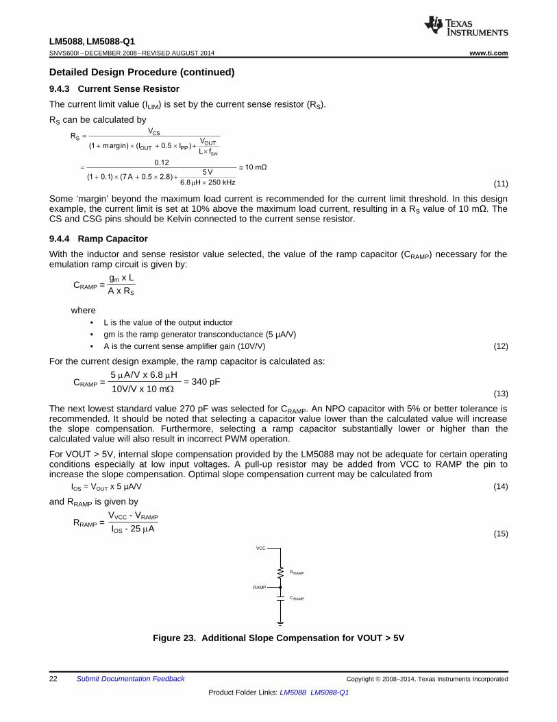
For VOUT > 5V, internal slope compensation provided by the LM5088 may not be adequate for certain operatingconditions especially at low input voltages. A pull-up resistor may be added from VCC to RAMP the pin toincrease the slope compensation. Optimal slope compensation current may be calculated from
IOS = VOUT x 5 µA/V (14)
and RRAMP is given by
(15)
Figure 23. Additional Slope Compensation for VOUT > 5V
22 Submit Documentation Feedback Copyright © 2008–2014, Texas Instruments Incorporated
Product Folder Links: LM5088 LM5088-Q1
'VIN =IOUT
4 x fSW x CIN= = 636 mV
7A4 x 250 kHz x 11 PF
CO =('V + VOUT)2 - VOUT
2
'IPPIO +2
L x2
LM5088, LM5088-Q1www.ti.com SNVS600I –DECEMBER 2008–REVISED AUGUST 2014
Detailed Design Procedure (continued)9.4.5 Output CapacitorsThe output capacitors smooth the inductor current ripple and provide a source of charge for load transientconditions. The output capacitor selection is primarily dictated by the following specifications:1. Steady-state output peak-peak ripple (ΔVPK-PK)2. Output voltage deviation during transient condition (ΔVTransient)
For the 5V output design example, ΔVPK-PK = 50 mV (1% of VOUT) and ΔTTransient = 100 mV (2% of VOUT) waschosen. The magnitude of output ripple primarily depends on ESR of the capacitors while load transient voltagedeviation depends both on the output capacitance and ESR.
When a full load is suddenly removed from the output, the output capacitor must be large enough to prevent theinductor energy to raise the output voltage above the specified maximum voltage. In other words, the outputcapacitor must be large enough to absorb the inductor’s maximum stored energy. Equating the stored energyequations of both the inductor and the output capacitor it can be shown that:
(16)
Evaluating, the above equation with a ΔVout of 100 mV results in an output capacitance of 475 µF. As statedearlier, the maximum peak to peak ripple primarily depends on the ESR of the output capacitor and the inductorripple current. To satisfy the ΔVPK-PK of 50 mV with 40% inductor current ripple, the ESR should be less than 15mΩ. In this design example a 470 µF aluminum capacitor with an ESR of 10 mΩ is paralleled with two 47 µFceramic capacitors to further reduce the ESR.
9.4.6 Input CapacitorsThe input power supply typically has large source impedance at the switching frequency. Good quality inputcapacitors are necessary to limit the ripple voltage at the VIN pin while supplying most of the switch currentduring the on-time. When the buck switch turns ON, the current into the external FET steps to the valley of theinductor current waveform at turn-on, ramps up to the peak value, and then drops to zero at turn-off. The inputcapacitors should be selected for RMS current rating and minimum ripple voltage. A good approximation for theripple current is IRMS > IOUT/2.
Quality ceramic capacitors with a low ESR should be selected for the input filter. To allow for capacitortolerances and voltage rating, five 2.2 µF, 100V ceramic capacitors were selected. With ceramic capacitors, theinput ripple voltage will be triangular and will peak at 50% duty cycle. Taking into account the capacitancechange with DC bias a worst case input peak-to-peak ripple voltage can be approximated as:
(17)
When the converter is connected to an input power source, a resonant circuit is formed by the line impedanceand the input capacitors. This can result in an overshoot at the VIN pin and could result in VIN exceeding itsabsolute maximum rating. Because of those conditions, it is recommended that either an aluminum typecapacitor with an ESR or increasing CIN>10 x LIN While using aluminum type capacitor care should be taken tonot exceed its maximum ripple current rating. Tantalum capacitors must be avoided at the input as they areprone to shorting.
Copyright © 2008–2014, Texas Instruments Incorporated Submit Documentation Feedback 23
Product Folder Links: LM5088 LM5088-Q1
RFB2
RFB1
VOUT
1.205V= -1
CSS =1.205V
tSS x 11 PA
CHB t'VHB
Qg
LM5088, LM5088-Q1SNVS600I –DECEMBER 2008–REVISED AUGUST 2014 www.ti.com
Detailed Design Procedure (continued)9.4.7 VCC CapacitorThe capacitor at the VCC pin provides noise filtering and stability for the VCC regulator. The recommended valueshould be no smaller than 0.1 µF, and should be a good quality, low ESR, ceramic capacitor. A value of 1 µFwas selected for this design.
9.4.8 Bootstrap CapacitorThe bootstrap capacitor between HB and SW pins supplies the gate current to charge the high-side MOSFETgate at each cycle’s turn-on as well as supplying the recovery charge for the bootstrap diode (D1).The peakcurrent can be several amperes. The recommended value of the bootstrap capacitor is at least 0.022 µF andshould be a good quality, low ESR, ceramic capacitor located close to the pins of the IC. The absolute minimumvalue for the bootstrap capacitor is calculated as:
where• Qg is the high-side MOSFET gate charge• ΔVHB is the tolerable voltage droop on CHB, which is typically less than 5% of the VCC (18)
.A value of 0.1 µF was selected for this design.
9.4.9 Soft-start CapacitorThe capacitor at the SS capacitor determines the soft-start time, the output voltage to reach the final regulatedvalue. The value of CSS for a given time is determined from:
(19)
For this design example, a value of 0.022 µF was chosen for a soft start time of approximately 2 ms.
9.4.10 Output Voltage DividerRFB1 and RFB2 set the output voltage level, the ratio of these resistors can be calculated from:
(20)
1.62 kΩ was chosen for RFB1 in this design which results in a RFB2 value of 5.11 kΩ. A reasonable guide is toselect the value of RFB1 value such that the current through the resistor (1.2V/ RFB1) is in between 1 mA and 100µA.
24 Submit Documentation Feedback Copyright © 2008–2014, Texas Instruments Incorporated
Product Folder Links: LM5088 LM5088-Q1
Trestart_delay =CRES x 1.2V
50 PA= CRES x 24k
RUV1 = 1.2V xRUV2
(VIN(min) + (5 PA x RUV2) - 1.2V)
LM5088, LM5088-Q1www.ti.com SNVS600I –DECEMBER 2008–REVISED AUGUST 2014
Detailed Design Procedure (continued)9.4.11 UVLO DividerA voltage divider can be connected to the EN pin to the set the minimum startup voltage (VIN(min)) of theregulator. If this feature is required, set the value of RUV2 between 10 kΩ and 100 kΩ and then calculate RUV1from:
(21)
In this design, for a VIN(min) of 5V, RUV2 was selected to be 54.9 kΩ resulting in a RUV1value of 16.2 kΩ. it isrecommended to install a capacitor parallel to RUV1 for filtering. If the EN pin is left open, the LM5088 will beginoperation once the upper VCC UV threshold of 4.0V (typ) is reached.
9.4.12 Restart Capacitor (LM5008-2 only)The basic operation of the hiccup mode current limit is described in Overload Protection Timer (LM5088-2 Only).In the LM5088-2 application example the RES pin is configured for delayed hiccup mode. Please refer toOverload Protection Timer (LM5088-2 Only) to configure this pin in alternate configurations and also refer toFigure 20. The delay time to initiate a hiccup cycle (t1) is programmed by the selection of RES pin capacitor. Inthe case of continuous cycle-by-cycle current limit detection at the CS pin, the time required for CRES to reach the1.2V is given by
(22)
The cool down time (t2) is set by the time taken to discharge the RES cap with 1.2 µA current source. Thisfeature will reduce the input power drawn by the converter during a prolonged over current condition. In thisapplication 500 µs of delay time was selected. The minimum value of CRES capacitor should be no less than0.022 µF.
9.4.13 MOSFET SelectionSelection of the Buck MOSFET is governed by the same tradeoffs as the switching frequency. Losses in powerMOSFETs can be broken down into conduction losses and switching losses. The conduction loss is given by:
PDC = D x (IO2 x RDS(ON) x 1.3)
where• D is the duty cycle• IO is the maximum load current (23)
The factor 1.3 accounts for the increase in MOSFET on-resistance due to heating. Alternatively, for a moreprecise calculation, the factor of 1.3 can be ignored and the on-resistance of the MOSFET can be estimatedusing the RDS(ON) vs. Temperature curves in the MOSFET datasheet.
The switching loss occurs during the brief transition period as the MOSFET turns on and off. During the transitionperiod both current and voltage are present in the MOSFET. The switching loss can be approximated as:
PSW = 0.5 x VIN x IO x (tR + tF) x fSW
where• tRthe rise time of the MOSFET• tF is the fall time of the MOSFET (24)
The rise and fall times are usually mentioned in the MOSFET datasheet or can be empirically observed on thescope. Another loss, which is associated with the buck MOSFET is the “gate-charging loss”. This loss differsfrom the above two losses in the sense that it is dissipated in the LM5088 and not in the MOSFET itself. Gatecharging loss, PGC, results from the current driving charging the gate capacitance of the power MOSFETs and isapproximated as:
PGC = VCC x Qg x fSW (25)
Copyright © 2008–2014, Texas Instruments Incorporated Submit Documentation Feedback 25
Product Folder Links: LM5088 LM5088-Q1
LM5088, LM5088-Q1SNVS600I –DECEMBER 2008–REVISED AUGUST 2014 www.ti.com
Detailed Design Procedure (continued)For this example with the maximum input voltage of 55V, the Vds breakdown rating of the selected MOSFETmust be greater than 55V plus any ringing across drain to source due to parasitics. In order to minimize switchingtime and gate drive losses, the selected MOSFET must also have low gate charge (Qg). A good choice ofMOSFET for this design example is the SI7148DP which has a total gate charge of 30nC and rise and fall timesof 10 ns and 12 ns respectively.
9.4.14 Diode SelectionA Schottky type re-circulating diode is required for all LM5088 applications. The near ideal reverse recoverycurrent transients and low forward voltage drop are particularly important diode characteristics for high inputvoltage and low output voltage applications common to LM5088. The diode switching loss is minimized in aSchottky diode because of near ideal reverse recovery. The conduction loss can be approximated by:
Pdc_diode = (1 - D) x IO x VF
where• VF is the forward drop of the diode (26)
The worst case is to assume a short circuit load condition. In this case, the diode will carry the output currentalmost continuously. The reverse breakdown rating should be selected for the maximum input voltage level plussome additional safety margin to withstand ringing at the SW node. For this application a 60V On SemiconductorSchottky diode (MBRB2060) with a specified forward drop of 0.6V at 7A at a junction temperature of 50°C wasselected. For output loads of 5A and greater and high input voltage applications, a diode in a D2PAK package isrecommended to support the worst case power dissipation
9.4.15 Snubber Components SelectionExcessive ringing and spikes can cause erratic operation and couple spikes and noise to the output. Voltagespikes beyond the rating of the LM5088 or the re-circulating diode can damage these devices. A snubbernetwork across the power diode reduces ringing and spikes at the switching node. Selecting the values for thesnubber is best accomplished through empirical methods. First, make sure that the lead lengths for the snubberconnections are very short. For the current levels typical for the LM5088, a resistor value between 3 and 10Ωshould be adequate. As a rule of thumb, a snubber capacitor which is 4~5 times the Schottky diode’s junctioncapacitance will reduce spikes adequately. Increasing the value of the snubber capacitor will result in moredamping but also results in higher losses. The resistor’s power dissipation is independent of the resistance valueas the resistor dissipates the energy stored by the snubber capacitor. The resistor’s power dissipation can beapproximated as:
PR_SNUB = CSNUB x VINmax2 x fSW (27)
26 Submit Documentation Feedback Copyright © 2008–2014, Texas Instruments Incorporated
Product Folder Links: LM5088 LM5088-Q1
-60
-40
-20
0
20
40
60
1.E+01 1.E+02 1.E+03 1.E+04 1.E+05
FREQUENCY (Hz)
GA
IN (
dB)
-200
-160
-120
-80
-40
0
40
80
PH
AS
E (
°)
120
160
200
LM5088, LM5088-Q1www.ti.com SNVS600I –DECEMBER 2008–REVISED AUGUST 2014
Detailed Design Procedure (continued)9.4.16 Error Amplifier CompensationRCOMP, CCOMP and CHF configure the error amplifier gain characteristics to accomplish a stable voltage loop gain.One advantage of current mode control is the ability of to close the loop with only two feedback componentsRCOMP and CCOMP. The voltage loop gain is the product of the modulator gain and the error amplifier gain. Forthis example, the modulator can be treated as an ideal voltage-to-current (transconductance) converter, The DCmodulator gain of the LM5088 can be modeled as:
DC Gain (MOD) = RLOAD/ (A x RS)
The dominant low frequency pole of the modulator is determined by the load resistance (RLOAD) and the outputcapacitance (COUT). The corner frequency of this pole is:
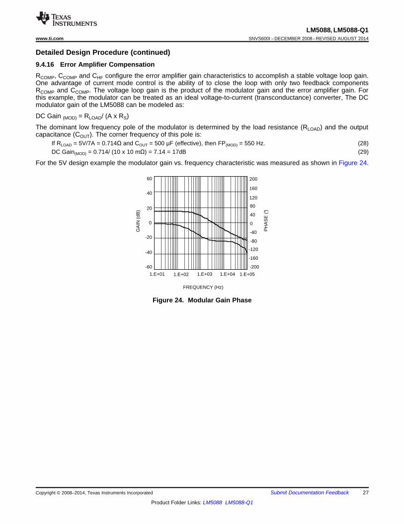
If RLOAD = 5V/7A = 0.714Ω and COUT = 500 µF (effective), then FP(MOD) = 550 Hz. (28)DC Gain(MOD) = 0.714/ (10 x 10 mΩ) = 7.14 = 17dB (29)
For the 5V design example the modulator gain vs. frequency characteristic was measured as shown in Figure 24.
Figure 24. Modular Gain Phase
Copyright © 2008–2014, Texas Instruments Incorporated Submit Documentation Feedback 27
Product Folder Links: LM5088 LM5088-Q1
-200
-160
-120
-80
-40
0
40
80
PH
AS
E (
°)
120
160
200
-60
-40
-20
0
20
40
60
GA
IN (
dB)
1.E+02 1.E+03 1.E+04 1.E+05
FREQUENCY (Hz)
-60
-40
-20
0
20
40
60
1.E+02 1.E+03 1.E+04 1.E+05 1.E+06
FREQUENCY (Hz)
GA
IN (
dB)
-200
-160
-120
-80
-40
0
40
80
PH
AS
E (
o )
120
160
200
LM5088, LM5088-Q1SNVS600I –DECEMBER 2008–REVISED AUGUST 2014 www.ti.com
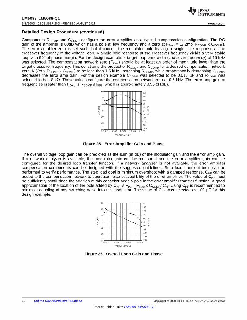
Detailed Design Procedure (continued)Components RCOMP and CCOMP configure the error amplifier as a type II compensation configuration. The DCgain of the amplifier is 80dB which has a pole at low frequency and a zero at FZero = 1/(2π x RCOMP x CCOMP).The error amplifier zero is set such that it cancels the modulator pole leaving a single pole response at thecrossover frequency of the voltage loop. A single pole response at the crossover frequency yields a very stableloop with 90° of phase margin. For the design example, a target loop bandwidth (crossover frequency) of 15 kHzwas selected. The compensation network zero (FZero) should be at least an order of magnitude lower than thetarget crossover frequency. This constrains the product of RCOMP and CCOMP for a desired compensation networkzero 1/ (2π x RCOMP x CCOMP) to be less than 1.5 kHz. Increasing RCOMP, while proportionally decreasing CCOMP,decreases the error amp gain. For the design example CCOMP was selected to be 0.015 µF and RCOMP wasselected to be 18 kΩ. These values configure the compensation network zero at 0.6 kHz. The error amp gain atfrequencies greater than FZero is RCOMP /RFB2, which is approximately 3.56 (11dB).
Figure 25. Error Amplifier Gain and Phase
The overall voltage loop gain can be predicted as the sum (in dB) of the modulator gain and the error amp gain.If a network analyzer is available, the modulator gain can be measured and the error amplifier gain can beconfigured for the desired loop transfer function. If a network analyzer is not available, the error amplifiercompensation components can be designed with the suggested guidelines. Step load transient tests can beperformed to verify performance. The step load goal is minimum overshoot with a damped response. CHF can beadded to the compensation network to decrease noise susceptibility of the error amplifier. The value of CHF mustbe sufficiently small since the addition of this capacitor adds a pole in the error amplifier transfer function. A goodapproximation of the location of the pole added by CHF is FP2 = FZero x CCOMP/ CHF.Using CHF is recommended tominimize coupling of any switching noise into the modulator. The value of CHF was selected as 100 pF for thisdesign example.
Figure 26. Overall Loop Gain and Phase
28 Submit Documentation Feedback Copyright © 2008–2014, Texas Instruments Incorporated
Product Folder Links: LM5088 LM5088-Q1
LM5088, LM5088-Q1www.ti.com SNVS600I –DECEMBER 2008–REVISED AUGUST 2014
Detailed Design Procedure (continued)9.4.17 Application CurvesSee Figure 24 through Figure 26 for Typical Application Curves.
10 Power Supply Recommendations
10.1 Thermal ConsiderationsIn a buck converter, most of the losses can be attributed to MOSFET conduction and switching loss, re-circulating diode conduction loss, inductor DCR loss and LM5088 VIN and VCC loss. The other dissipativecomponents in a buck converter produce losses but these other losses collectively account for about 2% of thetotal loss. Formulae to calculate all the major losses are described in their respective sections of this datasheet.The easiest method to determine the power dissipated within the LM5088 is to measure the total conversionlosses (Pin-Pout), then subtract the power losses in the Schottky diode, MOSFET, output inductor and snubberresistor. When operating at 7 A of output current and at 55 V, the power dissipation of the LM5088 isapproximately 850 mW. The junction to ambient thermal resistance of the LM5088 mounted in the evaluationboard is approximately 40°C with no airflow. At 25°C ambient temperature and no airflow, the predicted junctiontemperature will be 25+40*0.9 = 61°C. The LM5088 has an exposed thermal pad to aid in power dissipation.Adding several vias under the device will greatly reduce the controller junction temperature. The junction toambient thermal resistance will vary with application. The most significant variables are the area of copper in thePC board; the number of vias under the IC exposed pad and the amount of forced air cooling. The integrity ofsolder connection from the IC exposed pad to the PC board is critical. Excessive voids will greatly diminish thethermal dissipation capacity.
Copyright © 2008–2014, Texas Instruments Incorporated Submit Documentation Feedback 29
Product Folder Links: LM5088 LM5088-Q1

LM5088, LM5088-Q1SNVS600I –DECEMBER 2008–REVISED AUGUST 2014 www.ti.com
Figure 27. LM5088-1 Application Schematic
30 Submit Documentation Feedback Copyright © 2008–2014, Texas Instruments Incorporated
Product Folder Links: LM5088 LM5088-Q1

LM5088, LM5088-Q1www.ti.com SNVS600I –DECEMBER 2008–REVISED AUGUST 2014
Figure 28. LM5088-2 Application Schematic
Copyright © 2008–2014, Texas Instruments Incorporated Submit Documentation Feedback 31
Product Folder Links: LM5088 LM5088-Q1
ControllerVIN
GND
GND
VOUT
Inductor
CIN
CIN
COUTCOUT
RSQ
D
LM5088, LM5088-Q1SNVS600I –DECEMBER 2008–REVISED AUGUST 2014 www.ti.com
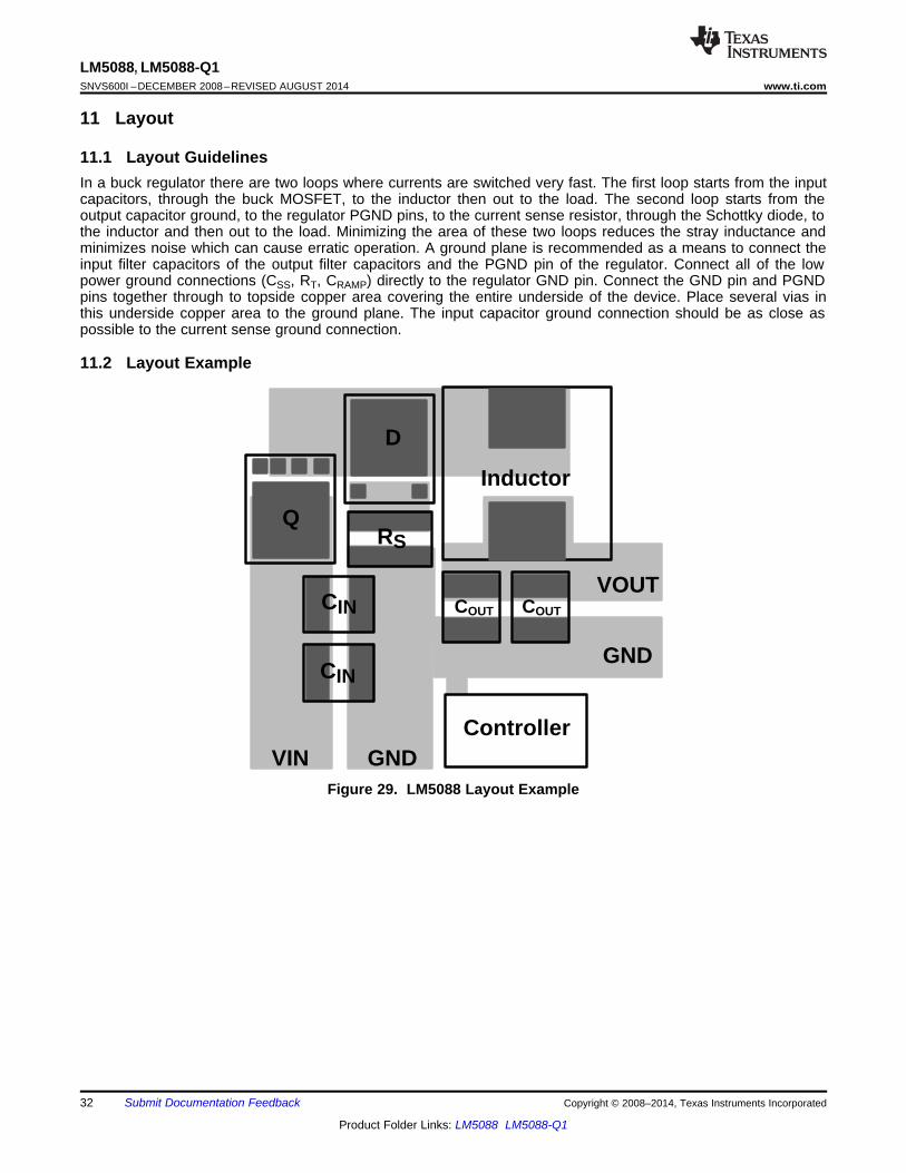
11 Layout
11.1 Layout GuidelinesIn a buck regulator there are two loops where currents are switched very fast. The first loop starts from the inputcapacitors, through the buck MOSFET, to the inductor then out to the load. The second loop starts from theoutput capacitor ground, to the regulator PGND pins, to the current sense resistor, through the Schottky diode, tothe inductor and then out to the load. Minimizing the area of these two loops reduces the stray inductance andminimizes noise which can cause erratic operation. A ground plane is recommended as a means to connect theinput filter capacitors of the output filter capacitors and the PGND pin of the regulator. Connect all of the lowpower ground connections (CSS, RT, CRAMP) directly to the regulator GND pin. Connect the GND pin and PGNDpins together through to topside copper area covering the entire underside of the device. Place several vias inthis underside copper area to the ground plane. The input capacitor ground connection should be as close aspossible to the current sense ground connection.
11.2 Layout Example
Figure 29. LM5088 Layout Example
32 Submit Documentation Feedback Copyright © 2008–2014, Texas Instruments Incorporated
Product Folder Links: LM5088 LM5088-Q1
LM5088, LM5088-Q1www.ti.com SNVS600I –DECEMBER 2008–REVISED AUGUST 2014
12 Device and Documentation Support
12.1 Related LinksThe table below lists quick access links. Categories include technical documents, support and communityresources, tools and software, and quick access to sample or buy.
Table 1. Related LinksTECHNICAL TOOLS & SUPPORT &PARTS PRODUCT FOLDER SAMPLE & BUY DOCUMENTS SOFTWARE COMMUNITY
LM5088 Click here Click here Click here Click here Click hereLM5088-Q1 Click here Click here Click here Click here Click here
12.2 TrademarksAll trademarks are the property of their respective owners.
12.3 Electrostatic Discharge CautionThese devices have limited built-in ESD protection. The leads should be shorted together or the device placed in conductive foamduring storage or handling to prevent electrostatic damage to the MOS gates.
12.4 GlossarySLYZ022 — TI Glossary.
This glossary lists and explains terms, acronyms, and definitions.
13 Mechanical, Packaging, and Orderable InformationThe following pages include mechanical, packaging, and orderable information. This information is the mostcurrent data available for the designated devices. This data is subject to change without notice and revision ofthis document. For browser-based versions of this data sheet, refer to the left-hand navigation.
Copyright © 2008–2014, Texas Instruments Incorporated Submit Documentation Feedback 33
Product Folder Links: LM5088 LM5088-Q1
PACKAGE OPTION ADDENDUM
www.ti.com 5-Aug-2014
Addendum-Page 1
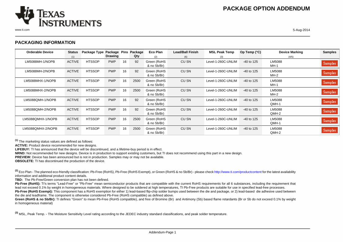
PACKAGING INFORMATION
Orderable Device Status(1)
Package Type PackageDrawing
Pins PackageQty
Eco Plan(2)
Lead/Ball Finish(6)
MSL Peak Temp(3)
Op Temp (°C) Device Marking(4/5)
Samples
LM5088MH-1/NOPB ACTIVE HTSSOP PWP 16 92 Green (RoHS& no Sb/Br)
CU SN Level-1-260C-UNLIM -40 to 125 LM5088MH-1
LM5088MH-2/NOPB ACTIVE HTSSOP PWP 16 92 Green (RoHS& no Sb/Br)
CU SN Level-1-260C-UNLIM -40 to 125 LM5088MH-2
LM5088MHX-1/NOPB ACTIVE HTSSOP PWP 16 2500 Green (RoHS& no Sb/Br)
CU SN Level-1-260C-UNLIM -40 to 125 LM5088MH-1
LM5088MHX-2/NOPB ACTIVE HTSSOP PWP 16 2500 Green (RoHS& no Sb/Br)
CU SN Level-1-260C-UNLIM -40 to 125 LM5088MH-2
LM5088QMH-1/NOPB ACTIVE HTSSOP PWP 16 92 Green (RoHS& no Sb/Br)
CU SN Level-1-260C-UNLIM -40 to 125 LM5088QMH-1
LM5088QMH-2/NOPB ACTIVE HTSSOP PWP 16 92 Green (RoHS& no Sb/Br)
CU SN Level-1-260C-UNLIM -40 to 125 LM5088QMH-2
LM5088QMHX-1/NOPB ACTIVE HTSSOP PWP 16 2500 Green (RoHS& no Sb/Br)
CU SN Level-1-260C-UNLIM -40 to 125 LM5088QMH-1
LM5088QMHX-2/NOPB ACTIVE HTSSOP PWP 16 2500 Green (RoHS& no Sb/Br)
CU SN Level-1-260C-UNLIM -40 to 125 LM5088QMH-2
(1) The marketing status values are defined as follows:ACTIVE: Product device recommended for new designs.LIFEBUY: TI has announced that the device will be discontinued, and a lifetime-buy period is in effect.NRND: Not recommended for new designs. Device is in production to support existing customers, but TI does not recommend using this part in a new design.PREVIEW: Device has been announced but is not in production. Samples may or may not be available.OBSOLETE: TI has discontinued the production of the device.
(2) Eco Plan - The planned eco-friendly classification: Pb-Free (RoHS), Pb-Free (RoHS Exempt), or Green (RoHS & no Sb/Br) - please check http://www.ti.com/productcontent for the latest availabilityinformation and additional product content details.TBD: The Pb-Free/Green conversion plan has not been defined.Pb-Free (RoHS): TI's terms "Lead-Free" or "Pb-Free" mean semiconductor products that are compatible with the current RoHS requirements for all 6 substances, including the requirement thatlead not exceed 0.1% by weight in homogeneous materials. Where designed to be soldered at high temperatures, TI Pb-Free products are suitable for use in specified lead-free processes.Pb-Free (RoHS Exempt): This component has a RoHS exemption for either 1) lead-based flip-chip solder bumps used between the die and package, or 2) lead-based die adhesive used betweenthe die and leadframe. The component is otherwise considered Pb-Free (RoHS compatible) as defined above.Green (RoHS & no Sb/Br): TI defines "Green" to mean Pb-Free (RoHS compatible), and free of Bromine (Br) and Antimony (Sb) based flame retardants (Br or Sb do not exceed 0.1% by weightin homogeneous material)
(3) MSL, Peak Temp. - The Moisture Sensitivity Level rating according to the JEDEC industry standard classifications, and peak solder temperature.
PACKAGE OPTION ADDENDUM
www.ti.com 5-Aug-2014
Addendum-Page 2
(4) There may be additional marking, which relates to the logo, the lot trace code information, or the environmental category on the device.
(5) Multiple Device Markings will be inside parentheses. Only one Device Marking contained in parentheses and separated by a "~" will appear on a device. If a line is indented then it is a continuationof the previous line and the two combined represent the entire Device Marking for that device.
(6) Lead/Ball Finish - Orderable Devices may have multiple material finish options. Finish options are separated by a vertical ruled line. Lead/Ball Finish values may wrap to two lines if the finishvalue exceeds the maximum column width.
Important Information and Disclaimer:The information provided on this page represents TI's knowledge and belief as of the date that it is provided. TI bases its knowledge and belief on informationprovided by third parties, and makes no representation or warranty as to the accuracy of such information. Efforts are underway to better integrate information from third parties. TI has taken andcontinues to take reasonable steps to provide representative and accurate information but may not have conducted destructive testing or chemical analysis on incoming materials and chemicals.TI and TI suppliers consider certain information to be proprietary, and thus CAS numbers and other limited information may not be available for release.
In no event shall TI's liability arising out of such information exceed the total purchase price of the TI part(s) at issue in this document sold by TI to Customer on an annual basis.
OTHER QUALIFIED VERSIONS OF LM5088, LM5088-Q1 :
• Catalog: LM5088
• Automotive: LM5088-Q1
NOTE: Qualified Version Definitions:
• Catalog - TI's standard catalog product
• Automotive - Q100 devices qualified for high-reliability automotive applications targeting zero defects

TAPE AND REEL INFORMATION
*All dimensions are nominal
Device PackageType
PackageDrawing
Pins SPQ ReelDiameter
(mm)
ReelWidth
W1 (mm)
A0(mm)
B0(mm)
K0(mm)
P1(mm)
W(mm)
Pin1Quadrant
LM5088MHX-1/NOPB HTSSOP PWP 16 2500 330.0 12.4 6.95 5.6 1.6 8.0 12.0 Q1
LM5088MHX-2/NOPB HTSSOP PWP 16 2500 330.0 12.4 6.95 5.6 1.6 8.0 12.0 Q1
LM5088QMHX-1/NOPB HTSSOP PWP 16 2500 330.0 12.4 6.95 5.6 1.6 8.0 12.0 Q1
LM5088QMHX-2/NOPB HTSSOP PWP 16 2500 330.0 12.4 6.95 5.6 1.6 8.0 12.0 Q1
PACKAGE MATERIALS INFORMATION
www.ti.com 14-Sep-2017
Pack Materials-Page 1

*All dimensions are nominal
Device Package Type Package Drawing Pins SPQ Length (mm) Width (mm) Height (mm)
LM5088MHX-1/NOPB HTSSOP PWP 16 2500 367.0 367.0 35.0
LM5088MHX-2/NOPB HTSSOP PWP 16 2500 367.0 367.0 35.0
LM5088QMHX-1/NOPB HTSSOP PWP 16 2500 367.0 367.0 35.0
LM5088QMHX-2/NOPB HTSSOP PWP 16 2500 367.0 367.0 35.0
PACKAGE MATERIALS INFORMATION
www.ti.com 14-Sep-2017
Pack Materials-Page 2
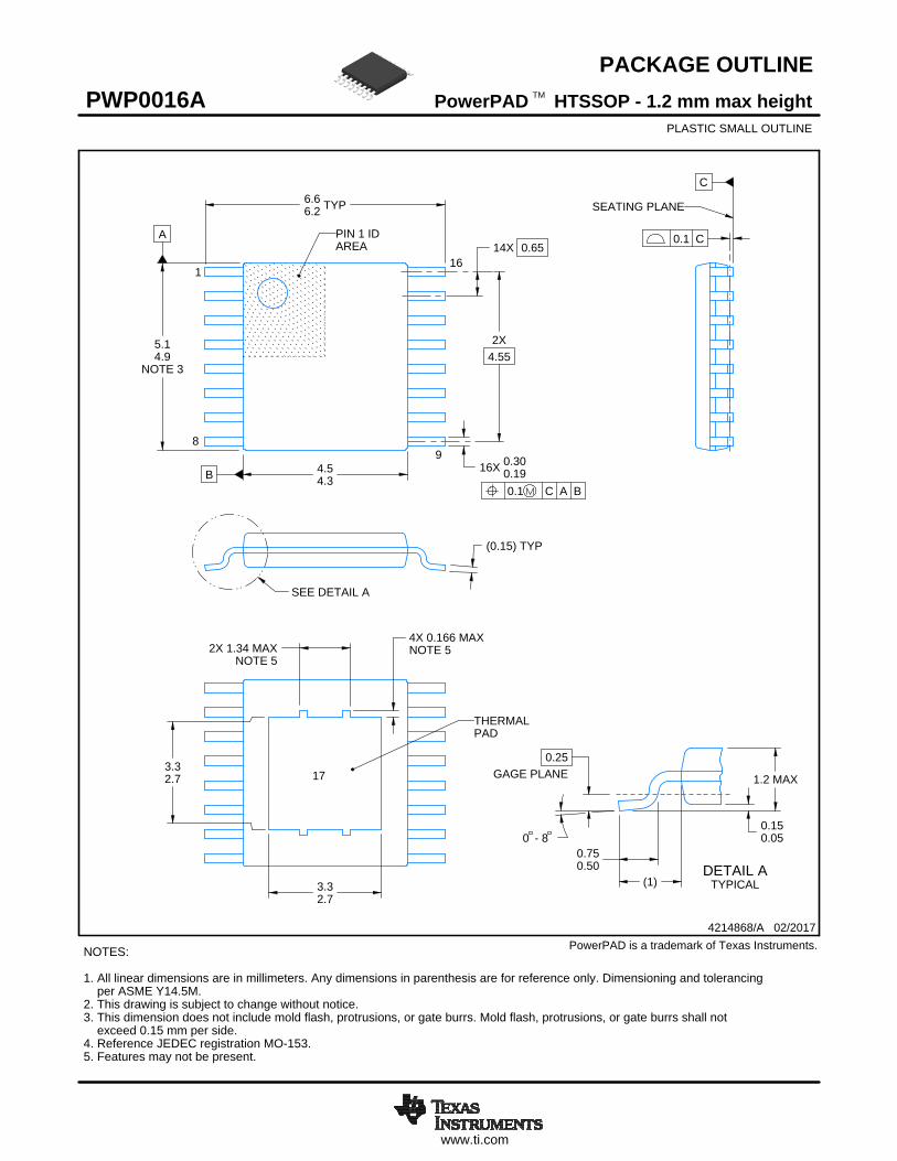
www.ti.com
PACKAGE OUTLINE
C
TYP6.66.2
14X 0.65
16X 0.300.19
2X4.55
(0.15) TYP
0 - 80.150.05
3.32.7
3.32.7
2X 1.34 MAXNOTE 5
1.2 MAX
(1)
0.25GAGE PLANE
0.750.50
A
NOTE 3
5.14.9
B 4.54.3
4X 0.166 MAXNOTE 5
4214868/A 02/2017
PowerPAD HTSSOP - 1.2 mm max heightPWP0016APLASTIC SMALL OUTLINE
NOTES: 1. All linear dimensions are in millimeters. Any dimensions in parenthesis are for reference only. Dimensioning and tolerancing per ASME Y14.5M. 2. This drawing is subject to change without notice. 3. This dimension does not include mold flash, protrusions, or gate burrs. Mold flash, protrusions, or gate burrs shall not exceed 0.15 mm per side.4. Reference JEDEC registration MO-153.5. Features may not be present.
PowerPAD is a trademark of Texas Instruments.
TM
116
0.1 C A B
98
PIN 1 IDAREA
SEATING PLANE
0.1 C
SEE DETAIL A
DETAIL ATYPICAL
SCALE 2.400
THERMALPAD
17
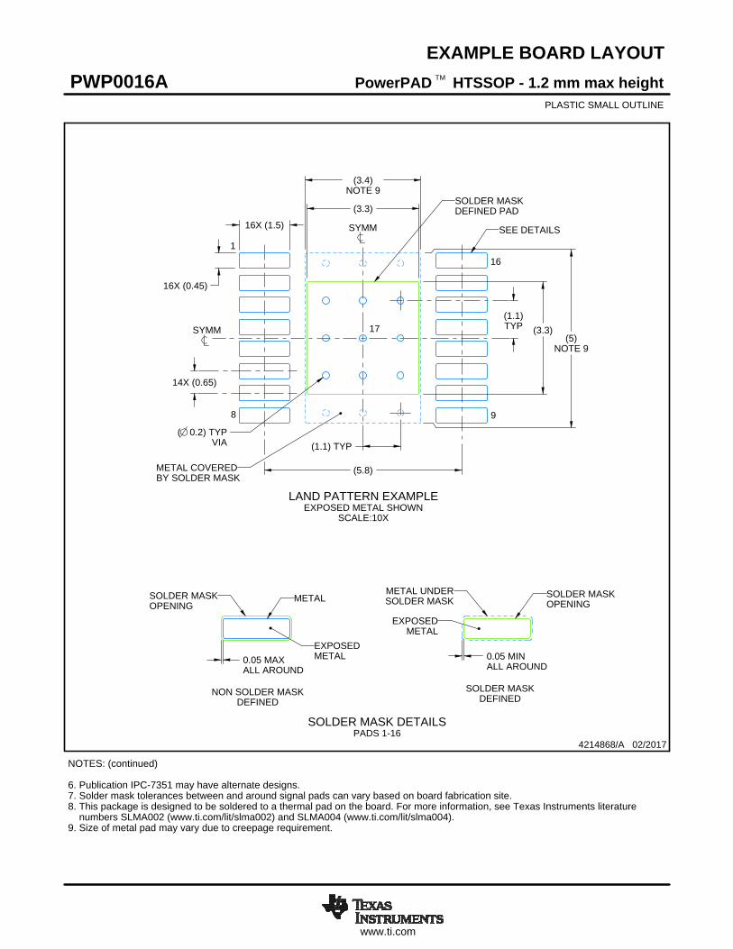
www.ti.com
EXAMPLE BOARD LAYOUT
(5.8)
0.05 MAXALL AROUND
0.05 MINALL AROUND
16X (1.5)
16X (0.45)
14X (0.65)
(3.4)NOTE 9
(5)NOTE 9
(3.3)
(3.3)
( 0.2) TYPVIA (1.1) TYP
(1.1)TYP
4214868/A 02/2017
PowerPAD HTSSOP - 1.2 mm max heightPWP0016APLASTIC SMALL OUTLINE
SYMM
SYMM
SEE DETAILS
LAND PATTERN EXAMPLEEXPOSED METAL SHOWN
SCALE:10X
1
8 9
16
METAL COVEREDBY SOLDER MASK
SOLDER MASKDEFINED PAD
17
NOTES: (continued) 6. Publication IPC-7351 may have alternate designs. 7. Solder mask tolerances between and around signal pads can vary based on board fabrication site. 8. This package is designed to be soldered to a thermal pad on the board. For more information, see Texas Instruments literature numbers SLMA002 (www.ti.com/lit/slma002) and SLMA004 (www.ti.com/lit/slma004).9. Size of metal pad may vary due to creepage requirement.
TM
METALSOLDER MASKOPENING
NON SOLDER MASKDEFINED
SOLDER MASK DETAILSPADS 1-16
EXPOSEDMETAL
SOLDER MASKDEFINED
SOLDER MASKMETAL UNDER SOLDER MASK
OPENING
EXPOSEDMETAL

www.ti.com
EXAMPLE STENCIL DESIGN
16X (1.5)
16X (0.45)
(3.3)
(3.3)BASED ON
0.125 THICKSTENCIL
14X (0.65)
(R0.05) TYP
(5.8)
4214868/A 02/2017
PowerPAD HTSSOP - 1.2 mm max heightPWP0016APLASTIC SMALL OUTLINE
2.79 X 2.790.1753.01 X 3.010.15
3.3 X 3.3 (SHOWN)0.1253.69 X 3.690.1
SOLDER STENCILOPENING
STENCILTHICKNESS
NOTES: (continued) 10. Laser cutting apertures with trapezoidal walls and rounded corners may offer better paste release. IPC-7525 may have alternate design recommendations. 11. Board assembly site may have different recommendations for stencil design.
TM
SYMM
SYMM
1
89
16
BASED ON0.125 THICK
STENCIL
BY SOLDER MASKMETAL COVERED
SEE TABLE FORDIFFERENT OPENINGSFOR OTHER STENCILTHICKNESSES
SOLDER PASTE EXAMPLEEXPOSED PAD
100% PRINTED SOLDER COVERAGE BY AREASCALE:10X
17
IMPORTANT NOTICE
Texas Instruments Incorporated (TI) reserves the right to make corrections, enhancements, improvements and other changes to itssemiconductor products and services per JESD46, latest issue, and to discontinue any product or service per JESD48, latest issue. Buyersshould obtain the latest relevant information before placing orders and should verify that such information is current and complete.TI’s published terms of sale for semiconductor products (http://www.ti.com/sc/docs/stdterms.htm) apply to the sale of packaged integratedcircuit products that TI has qualified and released to market. Additional terms may apply to the use or sale of other types of TI products andservices.Reproduction of significant portions of TI information in TI data sheets is permissible only if reproduction is without alteration and isaccompanied by all associated warranties, conditions, limitations, and notices. TI is not responsible or liable for such reproduceddocumentation. Information of third parties may be subject to additional restrictions. Resale of TI products or services with statementsdifferent from or beyond the parameters stated by TI for that product or service voids all express and any implied warranties for theassociated TI product or service and is an unfair and deceptive business practice. TI is not responsible or liable for any such statements.Buyers and others who are developing systems that incorporate TI products (collectively, “Designers”) understand and agree that Designersremain responsible for using their independent analysis, evaluation and judgment in designing their applications and that Designers havefull and exclusive responsibility to assure the safety of Designers' applications and compliance of their applications (and of all TI productsused in or for Designers’ applications) with all applicable regulations, laws and other applicable requirements. Designer represents that, withrespect to their applications, Designer has all the necessary expertise to create and implement safeguards that (1) anticipate dangerousconsequences of failures, (2) monitor failures and their consequences, and (3) lessen the likelihood of failures that might cause harm andtake appropriate actions. Designer agrees that prior to using or distributing any applications that include TI products, Designer willthoroughly test such applications and the functionality of such TI products as used in such applications.TI’s provision of technical, application or other design advice, quality characterization, reliability data or other services or information,including, but not limited to, reference designs and materials relating to evaluation modules, (collectively, “TI Resources”) are intended toassist designers who are developing applications that incorporate TI products; by downloading, accessing or using TI Resources in anyway, Designer (individually or, if Designer is acting on behalf of a company, Designer’s company) agrees to use any particular TI Resourcesolely for this purpose and subject to the terms of this Notice.TI’s provision of TI Resources does not expand or otherwise alter TI’s applicable published warranties or warranty disclaimers for TIproducts, and no additional obligations or liabilities arise from TI providing such TI Resources. TI reserves the right to make corrections,enhancements, improvements and other changes to its TI Resources. TI has not conducted any testing other than that specificallydescribed in the published documentation for a particular TI Resource.Designer is authorized to use, copy and modify any individual TI Resource only in connection with the development of applications thatinclude the TI product(s) identified in such TI Resource. NO OTHER LICENSE, EXPRESS OR IMPLIED, BY ESTOPPEL OR OTHERWISETO ANY OTHER TI INTELLECTUAL PROPERTY RIGHT, AND NO LICENSE TO ANY TECHNOLOGY OR INTELLECTUAL PROPERTYRIGHT OF TI OR ANY THIRD PARTY IS GRANTED HEREIN, including but not limited to any patent right, copyright, mask work right, orother intellectual property right relating to any combination, machine, or process in which TI products or services are used. Informationregarding or referencing third-party products or services does not constitute a license to use such products or services, or a warranty orendorsement thereof. Use of TI Resources may require a license from a third party under the patents or other intellectual property of thethird party, or a license from TI under the patents or other intellectual property of TI.TI RESOURCES ARE PROVIDED “AS IS” AND WITH ALL FAULTS. TI DISCLAIMS ALL OTHER WARRANTIES ORREPRESENTATIONS, EXPRESS OR IMPLIED, REGARDING RESOURCES OR USE THEREOF, INCLUDING BUT NOT LIMITED TOACCURACY OR COMPLETENESS, TITLE, ANY EPIDEMIC FAILURE WARRANTY AND ANY IMPLIED WARRANTIES OFMERCHANTABILITY, FITNESS FOR A PARTICULAR PURPOSE, AND NON-INFRINGEMENT OF ANY THIRD PARTY INTELLECTUALPROPERTY RIGHTS. TI SHALL NOT BE LIABLE FOR AND SHALL NOT DEFEND OR INDEMNIFY DESIGNER AGAINST ANY CLAIM,INCLUDING BUT NOT LIMITED TO ANY INFRINGEMENT CLAIM THAT RELATES TO OR IS BASED ON ANY COMBINATION OFPRODUCTS EVEN IF DESCRIBED IN TI RESOURCES OR OTHERWISE. IN NO EVENT SHALL TI BE LIABLE FOR ANY ACTUAL,DIRECT, SPECIAL, COLLATERAL, INDIRECT, PUNITIVE, INCIDENTAL, CONSEQUENTIAL OR EXEMPLARY DAMAGES INCONNECTION WITH OR ARISING OUT OF TI RESOURCES OR USE THEREOF, AND REGARDLESS OF WHETHER TI HAS BEENADVISED OF THE POSSIBILITY OF SUCH DAMAGES.Unless TI has explicitly designated an individual product as meeting the requirements of a particular industry standard (e.g., ISO/TS 16949and ISO 26262), TI is not responsible for any failure to meet such industry standard requirements.Where TI specifically promotes products as facilitating functional safety or as compliant with industry functional safety standards, suchproducts are intended to help enable customers to design and create their own applications that meet applicable functional safety standardsand requirements. Using products in an application does not by itself establish any safety features in the application. Designers mustensure compliance with safety-related requirements and standards applicable to their applications. Designer may not use any TI products inlife-critical medical equipment unless authorized officers of the parties have executed a special contract specifically governing such use.Life-critical medical equipment is medical equipment where failure of such equipment would cause serious bodily injury or death (e.g., lifesupport, pacemakers, defibrillators, heart pumps, neurostimulators, and implantables). Such equipment includes, without limitation, allmedical devices identified by the U.S. Food and Drug Administration as Class III devices and equivalent classifications outside the U.S.TI may expressly designate certain products as completing a particular qualification (e.g., Q100, Military Grade, or Enhanced Product).Designers agree that it has the necessary expertise to select the product with the appropriate qualification designation for their applicationsand that proper product selection is at Designers’ own risk. Designers are solely responsible for compliance with all legal and regulatoryrequirements in connection with such selection.Designer will fully indemnify TI and its representatives against any damages, costs, losses, and/or liabilities arising out of Designer’s non-compliance with the terms and provisions of this Notice.
Mailing Address: Texas Instruments, Post Office Box 655303, Dallas, Texas 75265Copyright © 2017, Texas Instruments Incorporated