Embed Size (px)
Citation preview
1SNVU545A–May 2017–Revised June 2017Submit Documentation Feedback
Copyright © 2017, Texas Instruments Incorporated
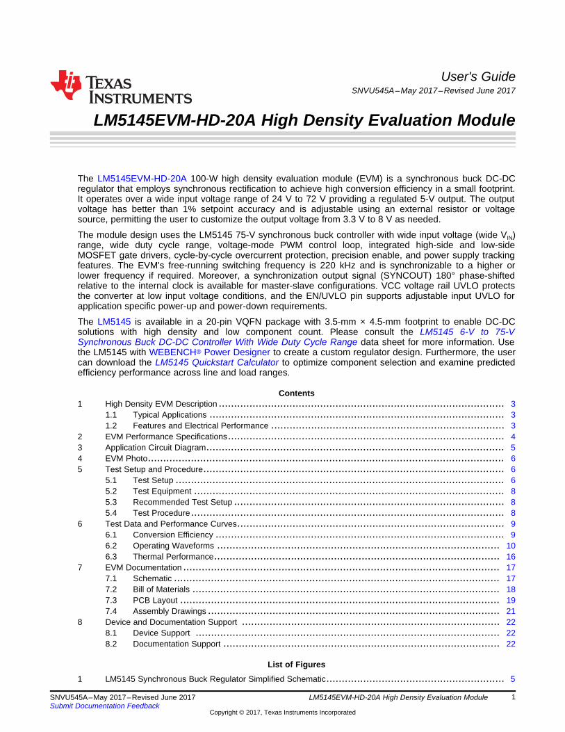
LM5145EVM-HD-20A High Density Evaluation Module
User's GuideSNVU545A–May 2017–Revised June 2017
LM5145EVM-HD-20A High Density Evaluation Module
The LM5145EVM-HD-20A 100-W high density evaluation module (EVM) is a synchronous buck DC-DCregulator that employs synchronous rectification to achieve high conversion efficiency in a small footprint.It operates over a wide input voltage range of 24 V to 72 V providing a regulated 5-V output. The outputvoltage has better than 1% setpoint accuracy and is adjustable using an external resistor or voltagesource, permitting the user to customize the output voltage from 3.3 V to 8 V as needed.
The module design uses the LM5145 75-V synchronous buck controller with wide input voltage (wide VIN)range, wide duty cycle range, voltage-mode PWM control loop, integrated high-side and low-sideMOSFET gate drivers, cycle-by-cycle overcurrent protection, precision enable, and power supply trackingfeatures. The EVM's free-running switching frequency is 220 kHz and is synchronizable to a higher orlower frequency if required. Moreover, a synchronization output signal (SYNCOUT) 180° phase-shiftedrelative to the internal clock is available for master-slave configurations. VCC voltage rail UVLO protectsthe converter at low input voltage conditions, and the EN/UVLO pin supports adjustable input UVLO forapplication specific power-up and power-down requirements.
The LM5145 is available in a 20-pin VQFN package with 3.5-mm × 4.5-mm footprint to enable DC-DCsolutions with high density and low component count. Please consult the LM5145 6-V to 75-VSynchronous Buck DC-DC Controller With Wide Duty Cycle Range data sheet for more information. Usethe LM5145 with WEBENCH® Power Designer to create a custom regulator design. Furthermore, the usercan download the LM5145 Quickstart Calculator to optimize component selection and examine predictedefficiency performance across line and load ranges.
Contents1 High Density EVM Description ............................................................................................. 3
1.1 Typical Applications ................................................................................................ 31.2 Features and Electrical Performance ............................................................................ 3
2 EVM Performance Specifications.......................................................................................... 43 Application Circuit Diagram................................................................................................. 54 EVM Photo.................................................................................................................... 65 Test Setup and Procedure.................................................................................................. 6
5.1 Test Setup ........................................................................................................... 65.2 Test Equipment ..................................................................................................... 85.3 Recommended Test Setup ........................................................................................ 85.4 Test Procedure...................................................................................................... 8
6 Test Data and Performance Curves....................................................................................... 96.1 Conversion Efficiency .............................................................................................. 96.2 Operating Waveforms ............................................................................................ 106.3 Thermal Performance............................................................................................. 16
7 EVM Documentation ....................................................................................................... 177.1 Schematic .......................................................................................................... 177.2 Bill of Materials .................................................................................................... 187.3 PCB Layout ........................................................................................................ 197.4 Assembly Drawings ............................................................................................... 21
8 Device and Documentation Support .................................................................................... 228.1 Device Support ................................................................................................... 228.2 Documentation Support .......................................................................................... 22
List of Figures
1 LM5145 Synchronous Buck Regulator Simplified Schematic.......................................................... 5
www.ti.com
2 SNVU545A–May 2017–Revised June 2017Submit Documentation Feedback
Copyright © 2017, Texas Instruments Incorporated
LM5145EVM-HD-20A High Density Evaluation Module
2 LM5145 EVM Photo ......................................................................................................... 63 EVM Test Setup ............................................................................................................. 74 Conversion Efficiency, FPWM Mode (SYNCIN Tied High)............................................................. 95 Conversion Efficiency, Diode Emulation Mode Enabled (SYNCIN Tied Low) ....................................... 96 SW Node Voltage and Output Ripple, IOUT = 20 A, VIN = 48 V........................................................ 107 SW Node and SYNCOUT Voltages, VIN = 48 V........................................................................ 108 Load Transient Response, VIN = 48 V, FPWM, 10 A to 20 A at 1 A/µs ............................................. 119 Load Transient Response, VIN = 48 V, FPWM, 0 A to 20 A at 1 A/µs .............................................. 1110 Input Voltage Rising Transient from 12 V to 72 V, IOUT = 10 A (ENABLE Terminal Tied High) .................. 1211 Input Voltage Falling Transient From 72 V to 12 V, IOUT = 10 A (ENABLE Terminal Tied High)................. 1212 ENABLE ON, VIN = 48 V, IOUT = 20 A Resistive ........................................................................ 1313 ENABLE OFF, VIN = 48 V, IOUT = 20 A Resistive ....................................................................... 1314 Start-Up, VIN = 48 V, IOUT = 20 A Resistive .............................................................................. 1415 Shutdown, VIN = 48 V, IOUT = 20 A Resistive ............................................................................ 1416 Pre-Biased Start-up, VIN = 48 V, IOUT = 0 A ............................................................................. 1517 Thermal Performance at VIN = 48 V, IOUT = 10 A, 200 LFM Airflow .................................................. 1618 Thermal Performance at VIN = 48 V, IOUT = 15 A, 200 LFM Airflow .................................................. 1619 EVM Schematic ............................................................................................................ 1720 Top Copper (Top View) ................................................................................................... 1921 Layer 2 Copper (Top View) ............................................................................................... 1922 Layer 3 Copper (Top View) ............................................................................................... 2023 Bottom Copper (Top View)................................................................................................ 2024 Top Assembly............................................................................................................... 2125 Bottom Assembly........................................................................................................... 21
List of Tables
1 Electrical Performance Specifications..................................................................................... 42 EVM Connections............................................................................................................ 63 Bill of Materials ............................................................................................................. 18
TrademarksWEBENCH is a registered trademark of Texas Instruments.All other trademarks are the property of their respective owners.
www.ti.com High Density EVM Description
3SNVU545A–May 2017–Revised June 2017Submit Documentation Feedback
Copyright © 2017, Texas Instruments Incorporated
LM5145EVM-HD-20A High Density Evaluation Module
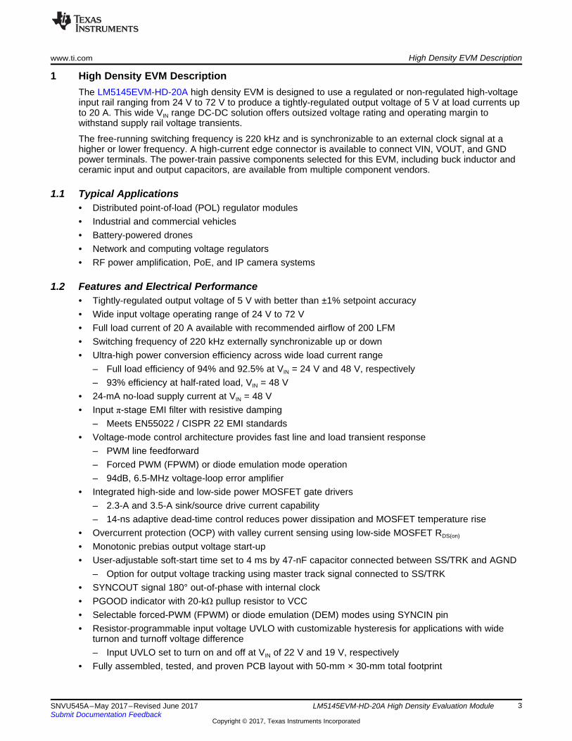
1 High Density EVM DescriptionThe LM5145EVM-HD-20A high density EVM is designed to use a regulated or non-regulated high-voltageinput rail ranging from 24 V to 72 V to produce a tightly-regulated output voltage of 5 V at load currents upto 20 A. This wide VIN range DC-DC solution offers outsized voltage rating and operating margin towithstand supply rail voltage transients.
The free-running switching frequency is 220 kHz and is synchronizable to an external clock signal at ahigher or lower frequency. A high-current edge connector is available to connect VIN, VOUT, and GNDpower terminals. The power-train passive components selected for this EVM, including buck inductor andceramic input and output capacitors, are available from multiple component vendors.
1.1 Typical Applications• Distributed point-of-load (POL) regulator modules• Industrial and commercial vehicles• Battery-powered drones• Network and computing voltage regulators• RF power amplification, PoE, and IP camera systems
1.2 Features and Electrical Performance• Tightly-regulated output voltage of 5 V with better than ±1% setpoint accuracy• Wide input voltage operating range of 24 V to 72 V• Full load current of 20 A available with recommended airflow of 200 LFM• Switching frequency of 220 kHz externally synchronizable up or down• Ultra-high power conversion efficiency across wide load current range
– Full load efficiency of 94% and 92.5% at VIN = 24 V and 48 V, respectively– 93% efficiency at half-rated load, VIN = 48 V
• 24-mA no-load supply current at VIN = 48 V• Input π-stage EMI filter with resistive damping
– Meets EN55022 / CISPR 22 EMI standards• Voltage-mode control architecture provides fast line and load transient response
– PWM line feedforward– Forced PWM (FPWM) or diode emulation mode operation– 94dB, 6.5-MHz voltage-loop error amplifier
• Integrated high-side and low-side power MOSFET gate drivers– 2.3-A and 3.5-A sink/source drive current capability– 14-ns adaptive dead-time control reduces power dissipation and MOSFET temperature rise
• Overcurrent protection (OCP) with valley current sensing using low-side MOSFET RDS(on)
• Monotonic prebias output voltage start-up• User-adjustable soft-start time set to 4 ms by 47-nF capacitor connected between SS/TRK and AGND
– Option for output voltage tracking using master track signal connected to SS/TRK• SYNCOUT signal 180° out-of-phase with internal clock• PGOOD indicator with 20-kΩ pullup resistor to VCC• Selectable forced-PWM (FPWM) or diode emulation (DEM) modes using SYNCIN pin• Resistor-programmable input voltage UVLO with customizable hysteresis for applications with wide
turnon and turnoff voltage difference– Input UVLO set to turn on and off at VIN of 22 V and 19 V, respectively
• Fully assembled, tested, and proven PCB layout with 50-mm × 30-mm total footprint

EVM Performance Specifications www.ti.com
4 SNVU545A–May 2017–Revised June 2017Submit Documentation Feedback
Copyright © 2017, Texas Instruments Incorporated
LM5145EVM-HD-20A High Density Evaluation Module
2 EVM Performance Specifications
(1) The default output voltage of this EVM is 5 V. Efficiency and other performance metrics can change based on operating inputvoltage, load current, externally-connected output capacitance, and other parameters.
(2) The recommended airflow when operating at output currents greater than 10 A is 200 LFM.
Table 1. Electrical Performance Specifications
PARAMETER TEST CONDITIONS MIN TYP MAX UNITINPUT CHARACTERISTICSInput voltage range, VIN Operating 24 48 72 VInput voltage turnon, VIN(ON)
Adjusted using EN/UVLO divider resistors22 V
Input voltage turnoff, VIN(OFF) 19 VInput voltage hysteresis, VIN(HYS) 3 V
Input current, no load, IIN(NL) IOUT = 0 AVIN = 24 V 26 mAVIN = 48 V 24 mAVIN = 72 V 20 mA
Input current, disabled, IIN(OFF) VEN = 0 V VIN = 48 V 1 mAOUTPUT CHARACTERISTICSOutput voltage, VOUT
(1) 4.95 5.0 5.05 VOutput current, IOUT VIN = 24 V to 75 V, Airflow = 200LFM (2) 0 20 A
Output voltage regulation, ΔVOUTLoad regulation IOUT = 0 A to 20 A 0.2%Line regulation VIN = 24 V to 72 V 0.2%
Output voltage ripple, VOUT(AC) VIN = 48 V, IOUT = 10 A 25 mVrmsOutput overcurrent protection, IOCP VIN = 48 V 25 ASoft-start time, tSS CSS = 47 nF 4 msSYSTEM CHARACTERISTICSSwitching frequency, FSW(nom) VIN = 48 V 220 kHzHalf-load efficiency, ηHALF
(1) IOUT = 10 A VIN = 24 V 95.5%VIN = 36 V 94.5%VIN = 48 V 94%VIN = 72 V 91%
Full load efficiency, ηFULL IOUT = 20 A
VIN = 24 V 94%VIN = 36 V 93.5%VIN = 48 V 92.5%VIN = 72 V 90.5%
LM5145 junction temperature, TJ –40 125 ºC
1
2
3
4
5
6
7
10 11
17
18
19
14
20
BST
HO
SW
LO
PGND
RT
SS/TRK
COMP
FB
AGND
VIN
VOUTLM5145
VOUT
SYNC GND
PG
12
SYNCOUT
8 SYNCIN
9 NC
EN/UVLO VIN
ILIMPGOOD
SYNC out
13
VCC
16
15
NC
EP
LF
COUT
Q1
Q2
CIN
RILIM
CVCC
CBST
CSS
RUV2 RUV1
RFB2
RFB1
RC2
CC2
CC1RC1
CC3
RPG
optional
RRT
Copyright © 2017, Texas Instruments Incorporated
CILIM
www.ti.com Application Circuit Diagram
5SNVU545A–May 2017–Revised June 2017Submit Documentation Feedback
Copyright © 2017, Texas Instruments Incorporated
LM5145EVM-HD-20A High Density Evaluation Module
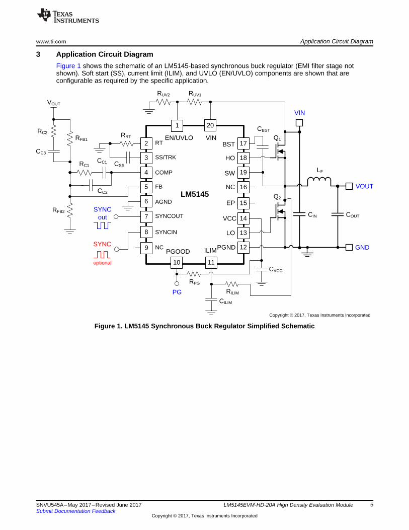
3 Application Circuit DiagramFigure 1 shows the schematic of an LM5145-based synchronous buck regulator (EMI filter stage notshown). Soft start (SS), current limit (ILIM), and UVLO (EN/UVLO) components are shown that areconfigurable as required by the specific application.
Figure 1. LM5145 Synchronous Buck Regulator Simplified Schematic
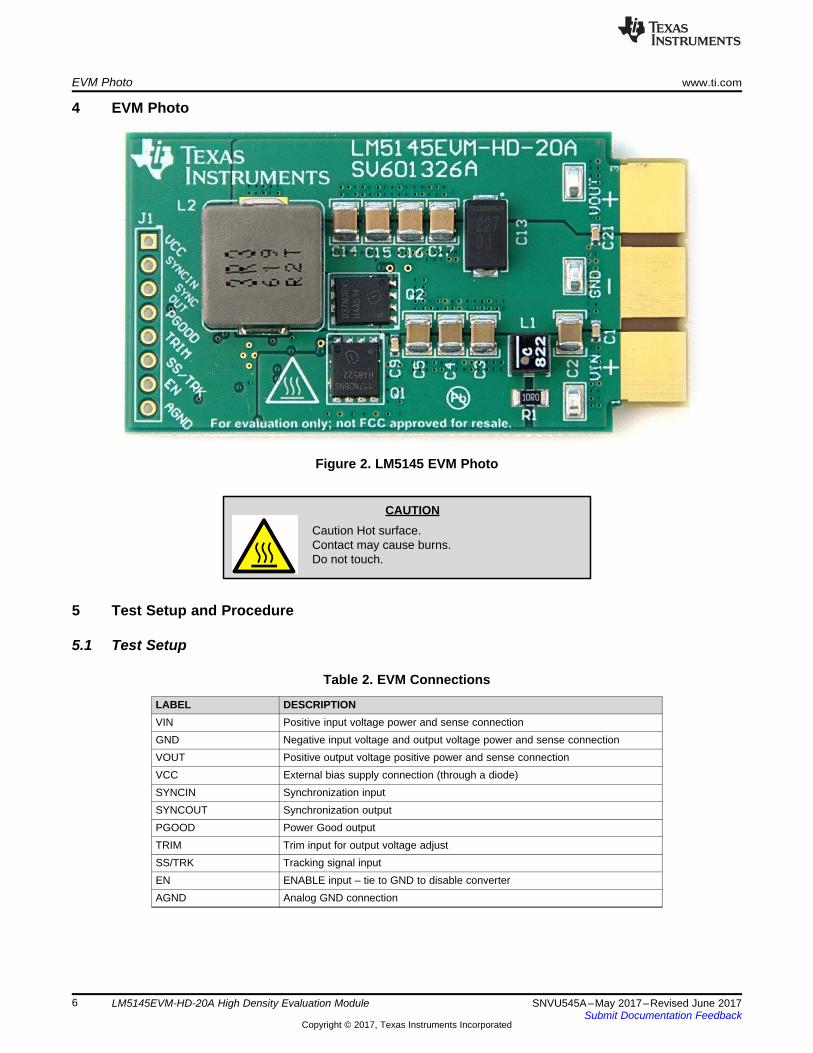
CAUTION
Caution Hot surface.Contact may cause burns.Do not touch.
EVM Photo www.ti.com
6 SNVU545A–May 2017–Revised June 2017Submit Documentation Feedback
Copyright © 2017, Texas Instruments Incorporated
LM5145EVM-HD-20A High Density Evaluation Module
4 EVM Photo
Figure 2. LM5145 EVM Photo
5 Test Setup and Procedure
5.1 Test Setup
Table 2. EVM Connections
LABEL DESCRIPTIONVIN Positive input voltage power and sense connectionGND Negative input voltage and output voltage power and sense connectionVOUT Positive output voltage positive power and sense connectionVCC External bias supply connection (through a diode)SYNCIN Synchronization inputSYNCOUT Synchronization outputPGOOD Power Good outputTRIM Trim input for output voltage adjustSS/TRK Tracking signal inputEN ENABLE input – tie to GND to disable converterAGND Analog GND connection

A COM
Ammeter 1 Electronic Load
+ -
VVoltmeter 1
COM VVoltmeter 2
COM
Oscilloscope
+-
Power Supply
A COM
Ammeter 2
www.ti.com Test Setup and Procedure
7SNVU545A–May 2017–Revised June 2017Submit Documentation Feedback
Copyright © 2017, Texas Instruments Incorporated
LM5145EVM-HD-20A High Density Evaluation Module
Referencing the EVM connections described in Table 2, the recommended test setup to evaluate theLM5145EVM-HD-20A is shown in Figure 3. Working at an ESD-protected workstation, make sure that anywrist straps, boot straps, or mats are connected and referencing the user to earth ground before power isapplied to the EVM.
Figure 3. EVM Test Setup
SPACER
CAUTIONRefer to the LM5145 datasheet, LM5145 Quickstart Calculator andWEBENCH® Power Designer for additional guidance pertaining to componentselection and converter operation.
Test Setup and Procedure www.ti.com
8 SNVU545A–May 2017–Revised June 2017Submit Documentation Feedback
Copyright © 2017, Texas Instruments Incorporated
LM5145EVM-HD-20A High Density Evaluation Module
5.2 Test EquipmentVoltage Source: The input voltage source VIN should be a 0–72-V variable DC source capable ofsupplying 10 A.
Multimeters:• Voltmeter 1: Input voltage at VIN to GND. Set voltmeter to an input impedance of 100 MΩ.• Voltmeter 2: Output voltage at VOUT to GND. Set voltmeter to an input impedance of 100 MΩ.• Ammeter 1: Input current. Set ammeter to 1-second aperture time.• Ammeter 2: Output current. Set ammeter to 1-second aperture time
Electronic Load: The load should be an electronic constant-resistance (CR) or constant-current (CC)mode load capable of 0 Adc to 20 Adc at 5 V. For a no-load input current measurement, disconnect theelectronic load as it may draw a small residual current.
Oscilloscope: With the scope set to 20-MHz bandwidth and AC coupling, measure the output voltageripple directly across an output capacitor with a short ground lead normally provided with the scope probe.Place the oscilloscope probe tip on the positive terminal of the output capacitor, holding the probe'sground barrel through the ground lead to the capacitor's negative terminal. TI does not recommend usinga long-leaded ground connection because this may induce additional noise given a large ground loop. Tomeasure other waveforms, adjust the oscilloscope as needed.
Safety: Always use caution when touching any circuits that may be live or energized.
5.3 Recommended Test Setup
5.3.1 Input Connections• Prior to connecting the DC input source, set the current limit of the input supply to 0.1 A maximum.
Ensure the input source is initially set to 0 V and connected to the VIN and GND connection points asshown in Figure 3. An additional input bulk capacitor is recommended to provide damping if long inputlines are used.
• Connect voltmeter 1 at VIN and GND connection points to measure the input voltage.• Connect ammeter 1 to measure the input current and set to at least 1-second aperture time.
5.3.2 Output Connections• Connect an electronic load to VOUT and GND connections. Set the load to constant-resistance mode
or constant-current mode at 0 A before applying input voltage.• Connect voltmeter 2 at VOUT and GND connection points to measure the output voltage.• Connect ammeter 2 to measure the output current.
5.4 Test Procedure
5.4.1 Line and Load Regulation, Efficiency• Set up the EVM as described above.• Set load to constant resistance or constant current mode and to sink 0 A.• Increase input source from 0 V to 48 V; use voltmeter 1 to measure the input voltage.• Increase the current limit of the input supply to 10A.• Using voltmeter 2 to measure the output voltage, VOUT, vary the load current from 0 to 20 A DC; VOUT
should remain within the load regulation specification.• Set the load current to 10 A (50% rated load) and vary the input source voltage from 24 V to 72 V; VOUT
should remain within the line regulation specification.• Decrease load to 0 A. Decrease input source voltage to 0 V.
Output Current (A)
Effi
cien
cy (
%)
0.1 0.5 1 5 10 202020
30
40
50
60
70
80
90
100
VIN = 12VVIN = 24VVIN = 36VVIN = 48VVIN = 60VVIN = 75V
Output Current (A)
Effi
cien
cy (
%)
0 5 10 15 2065
70
75
80
85
90
95
100
VIN = 12VVIN = 24VVIN = 36VVIN = 48VVIN = 60VVIN = 75V
www.ti.com Test Data and Performance Curves
9SNVU545A–May 2017–Revised June 2017Submit Documentation Feedback
Copyright © 2017, Texas Instruments Incorporated
LM5145EVM-HD-20A High Density Evaluation Module
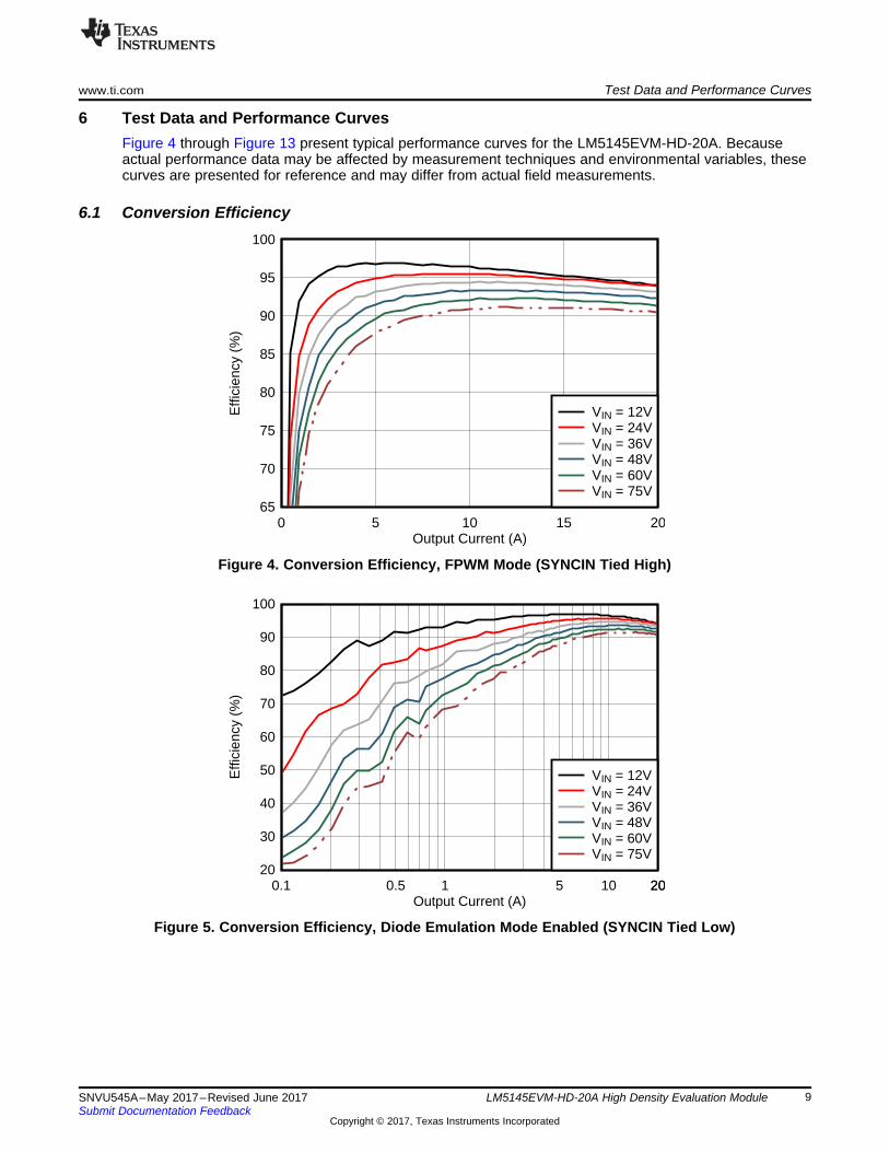
6 Test Data and Performance CurvesFigure 4 through Figure 13 present typical performance curves for the LM5145EVM-HD-20A. Becauseactual performance data may be affected by measurement techniques and environmental variables, thesecurves are presented for reference and may differ from actual field measurements.
6.1 Conversion Efficiency
Figure 4. Conversion Efficiency, FPWM Mode (SYNCIN Tied High)
Figure 5. Conversion Efficiency, Diode Emulation Mode Enabled (SYNCIN Tied Low)
SYNCOUT 1V/DIV
SW 10V/DIV
2 Ps/DIV
VOUT50mV/DIV
SW 10V/DIV
2 Ps/DIV
Test Data and Performance Curves www.ti.com
10 SNVU545A–May 2017–Revised June 2017Submit Documentation Feedback
Copyright © 2017, Texas Instruments Incorporated
LM5145EVM-HD-20A High Density Evaluation Module
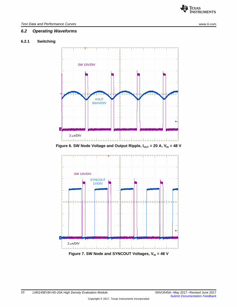
6.2 Operating Waveforms
6.2.1 Switching
Figure 6. SW Node Voltage and Output Ripple, IOUT = 20 A, VIN = 48 V
Figure 7. SW Node and SYNCOUT Voltages, VIN = 48 V
VOUT 500m/DIV
40 Ps/DIV
IOUT 5A/DIV
VOUT 200m/DIV
40 Ps/DIV
IOUT 5A/DIV
www.ti.com Test Data and Performance Curves
11SNVU545A–May 2017–Revised June 2017Submit Documentation Feedback
Copyright © 2017, Texas Instruments Incorporated
LM5145EVM-HD-20A High Density Evaluation Module
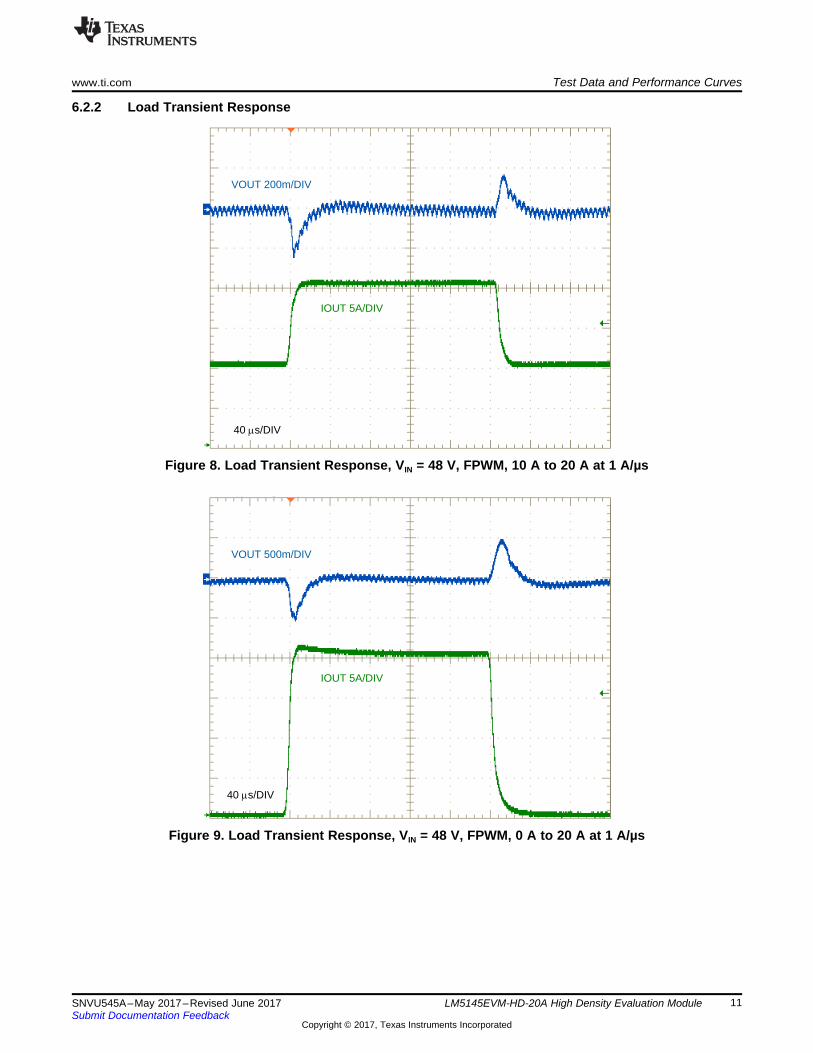
6.2.2 Load Transient Response
Figure 8. Load Transient Response, VIN = 48 V, FPWM, 10 A to 20 A at 1 A/µs
Figure 9. Load Transient Response, VIN = 48 V, FPWM, 0 A to 20 A at 1 A/µs
VOUT 50mV/DIV
VIN 20V/DIV
20 ms/DIV
IOUT 5A/DIV
VOUT 50mV/DIV
VIN 20V/DIV
20 ms/DIV
IOUT 5A/DIV
Test Data and Performance Curves www.ti.com
12 SNVU545A–May 2017–Revised June 2017Submit Documentation Feedback
Copyright © 2017, Texas Instruments Incorporated
LM5145EVM-HD-20A High Density Evaluation Module
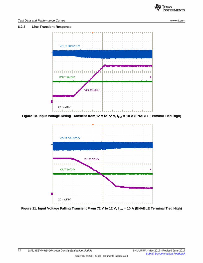
6.2.3 Line Transient Response
Figure 10. Input Voltage Rising Transient from 12 V to 72 V, IOUT = 10 A (ENABLE Terminal Tied High)
Figure 11. Input Voltage Falling Transient From 72 V to 12 V, IOUT = 10 A (ENABLE Terminal Tied High)
PGOOD 2V/DIV
VOUT 1V/DIV
ENABLE1V/DIV
40 Ps/DIV
IOUT 5A/DIV
PGOOD 2V/DIV
VOUT 1V/DIV
ENABLE1V/DIV
1 ms/DIV
IOUT 5A/DIV
www.ti.com Test Data and Performance Curves
13SNVU545A–May 2017–Revised June 2017Submit Documentation Feedback
Copyright © 2017, Texas Instruments Incorporated
LM5145EVM-HD-20A High Density Evaluation Module
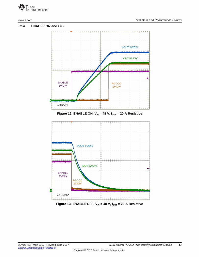
6.2.4 ENABLE ON and OFF
Figure 12. ENABLE ON, VIN = 48 V, IOUT = 20 A Resistive
Figure 13. ENABLE OFF, VIN = 48 V, IOUT = 20 A Resistive

PGOOD 2V/DIV
VOUT 1V/DIV
VIN 10V/DIV
200 Ps/DIV
IOUT 5A/DIV
PGOOD 2V/DIV
VOUT 1V/DIV
VIN 10V/DIV
1 ms/DIV
IOUT 5A/DIV
Test Data and Performance Curves www.ti.com
14 SNVU545A–May 2017–Revised June 2017Submit Documentation Feedback
Copyright © 2017, Texas Instruments Incorporated
LM5145EVM-HD-20A High Density Evaluation Module
6.2.5 Start-Up
Figure 14. Start-Up, VIN = 48 V, IOUT = 20 A Resistive
Figure 15. Shutdown, VIN = 48 V, IOUT = 20 A Resistive
PGOOD 2V/DIV
VOUT 1V/DIV
VIN 10V/DIV
2 ms/DIV
www.ti.com Test Data and Performance Curves
15SNVU545A–May 2017–Revised June 2017Submit Documentation Feedback
Copyright © 2017, Texas Instruments Incorporated
LM5145EVM-HD-20A High Density Evaluation Module
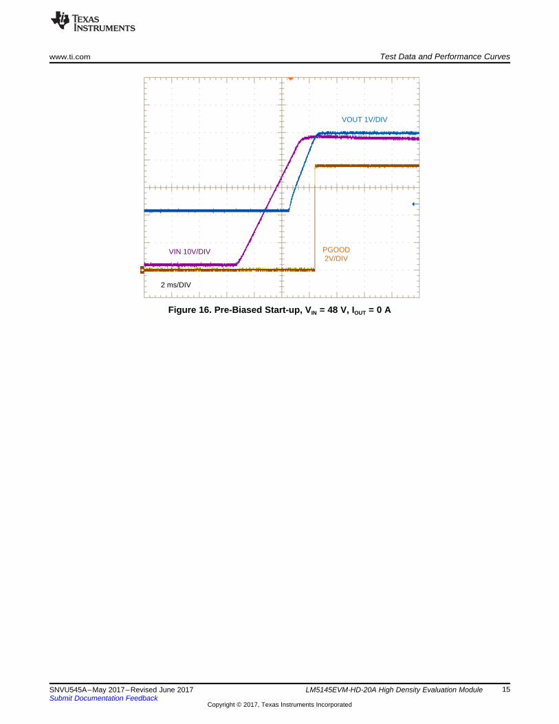
Figure 16. Pre-Biased Start-up, VIN = 48 V, IOUT = 0 A

Test Data and Performance Curves www.ti.com
16 SNVU545A–May 2017–Revised June 2017Submit Documentation Feedback
Copyright © 2017, Texas Instruments Incorporated
LM5145EVM-HD-20A High Density Evaluation Module
6.3 Thermal Performance
Figure 17. Thermal Performance at VIN = 48 V, IOUT = 10 A, 200 LFM Airflow
Figure 18. Thermal Performance at VIN = 48 V, IOUT = 15 A, 200 LFM Airflow
EN/UVLO1
RT2
SS/TRK3
COMP4
FB5
AGND6
SYNCOUT7
SYNCIN8
NC9
PGOOD10
ILIM11
PGND12
LO13
VCC14
EP15
NC16
BST17
HO18
SW19
VIN20
EP21
U1
LM5145RGYR
7,8
1,2
,3
5,6
,
Q1BSC117N08NS5ATMA1
47µFC17
47µFC16
47µFC15
0.1µF
C11
2.2µFC22
422
R5
PGND
PGND
PGND
PGND
10.0kR9
NT2
Net-Tie
AGND
5600pFC23
150pFC24
PGND
VCC
VIN
C13220µF
VIN
0.047µFC25
46.4kR11
18.2kR10
301kR2
0.1µF
C10
20.0kR6
VCC
3.83k
R12
20.0k
R13
1.00k
R16
1800pF
C26
3.3µH
L2
100pFC12DNP
2.20R8
DNP
2.2R3
1 2 3
NC
4
5 6 7 8 9
D1
100V
0
R4
4.7µFC8
4.7µFC7
TP1
TP2
TP3
PGND
4.7µFC6
47µFC14
49.9
R14
29.4kR15
NT1
Net-Tie
20.0kR7
8.2µH
L1
4.7µFC2
10.0
R1
BOTTOP
1 2
3 4
5 6
EC1
7,8
1,2
,3
5,6
, Q2BSC037N08NS5ATMA1
VOUT
PGND PGND
V+ V+VOUT VOUT
5
4
1
2
3
6
7
8
J1
DNP
EN
SYNCINSYNCOUT
PGOODTRIM
AGND
47µFC19
47µFC18
4.7µFC4
4.7µFC5
4.7µFC3
47µFC20
SS\TRK
VCC
HO
0.01µFC9
0.01µFC1
0.01µFC21
15pF
C27
PGND
AGND*
VIN = 24-72VDC
VOUT = 5.0V @ 20A
Copyright © 2017, Texas Instruments Incorporated
www.ti.com EVM Documentation
17SNVU545A–May 2017–Revised June 2017Submit Documentation Feedback
Copyright © 2017, Texas Instruments Incorporated
LM5145EVM-HD-20A High Density Evaluation Module
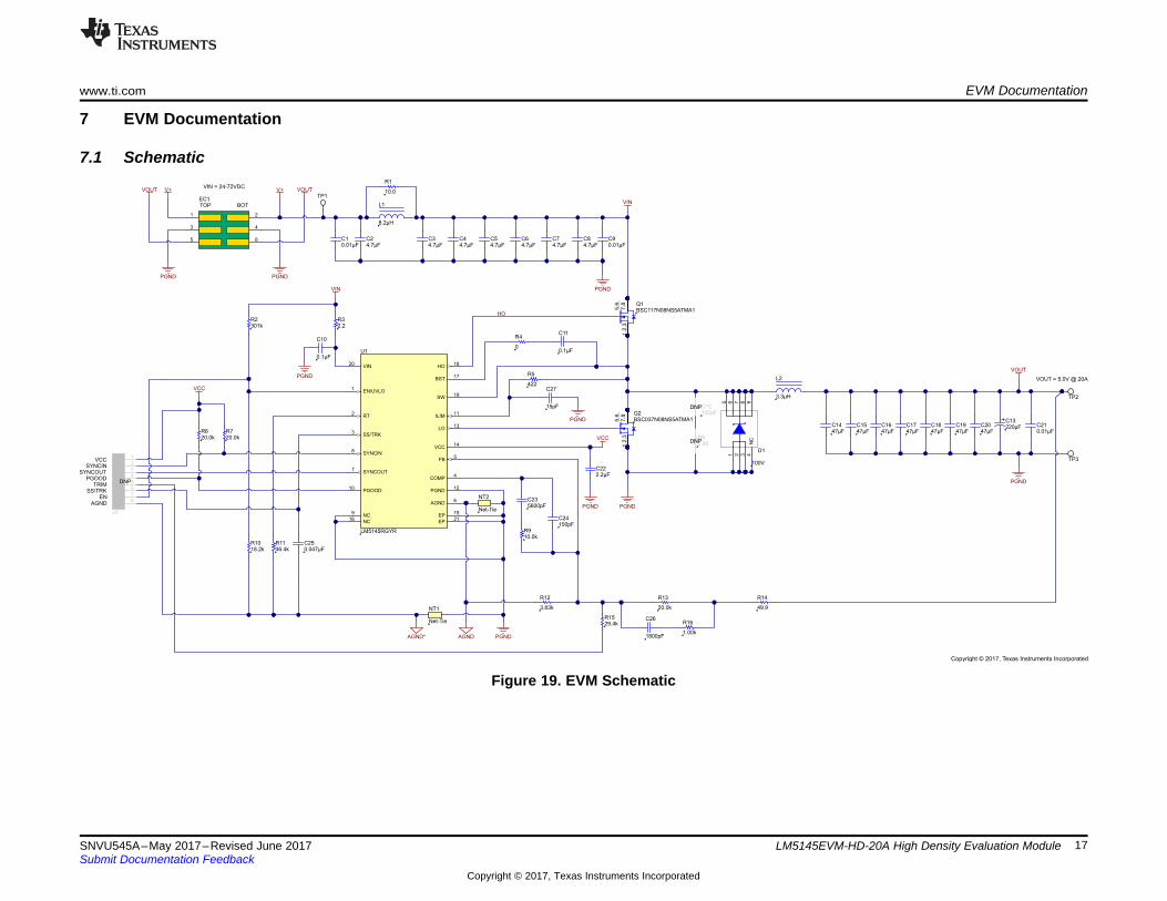
7 EVM Documentation
7.1 Schematic
Figure 19. EVM Schematic
EVM Documentation www.ti.com
18 SNVU545A–May 2017–Revised June 2017Submit Documentation Feedback
Copyright © 2017, Texas Instruments Incorporated
LM5145EVM-HD-20A High Density Evaluation Module
7.2 Bill of Materials
Table 3. Bill of MaterialsCOUNT REF DES DESCRIPTION PART NUMBER MFR
3 C1, C9, C21 Capacitor, Ceramic, 10nF, 100V, X7R, 0603 Std Std
7 C2, C3, C4, C5,C6, C7, C8 Capacitor, Ceramic, 4.7μF, 100V, X7S, 1210
C3225X7S2A475M200AB TDK
GRJ32DC72A475KE11L Murata
1 C10 Capacitor, Ceramic, 0.1μF, 100V, X7R, 0603 C1608X7R1A105K080AC TDK
1 C11 Capacitor, Ceramic, 0.1μF, 25V, X7R, 0603 Std Std
1 C13Capacitor, Polymer Aluminum, 220μF, 6.3V, 7343, 10mΩ ESR ECASD60J227M010K00 Murata
Capacitor, Tant Polymer, 220μF, 10V, 7343, 18mΩ ESR 10TCE220MIL Panasonic
7C14, C15, C16,C17, C18, C19,C20
Capacitor, Ceramic, 47μF, 10V, X7R, 1210
GRM32ER71A476KE15L Murata
LMK325B7476MM-TR Taiyo Yuden
1210ZC476KAT2A AVX
1 C22Capacitor, Ceramic, 2.2μF, 16V, X7R, 0603 EMK107BB7225MA-T Taiyo Yuden
Capacitor, Ceramic, 2.2μF, 16V, X7S, 0603 GRM188C71C225KE11D Murata
1 C23 Capacitor, Ceramic, 5.6nF, 16V, X7R, 10%, 0603 Std Std
1 C24 Capacitor, Ceramic, 150pF, 16V, X7R, 10%, 0603 Std Std
1 C25 Capacitor, Ceramic, 47nF, 16V, X7R, 10%, 0603 Std Std
1 C26 Capacitor, Ceramic, 1.8nF, 16V, X7R, 10%, 0603 Std Std
1 C27 Capacitor, Ceramic, 15pF, 100V, X7R, 10%, 0603 Std Std
1 D1 Schottky Diode, 100V, 6A ST STPS6M100
1 L1 Inductor, 8.2µH ±20%, 60mΩ max, 3.4A Isat, 4mm max XAL4040-822MEC Coilcraft
1 L2
Inductor, 3.3µH ±20%, 3.75mΩ typ, 42A, 6.5mm max CMLS136E-3R3MS Cyntec
Inductor, 3.3μH, 5.7mΩ typ, 32 A, 6.5mm max 744373965033 Würth Electronik
Inductor, 3.0μH, 5.86mΩ typ, 37 A, 5mm max XAL1350-302MED Coilcraft
1 Q1 MOSFET, N-Channel, 80V, 12mΩ BSC117N08NS5 Infineon
1 Q2 MOSFET, N-Channel, 80V, 4mΩ BSC037N08NS5 Infineon
1 R1 Resistor, Chip, 10Ω, 1/8W, 5%, 1206 Std Std
1 R2 Resistor, Chip, 301kΩ, 1/16W, 1%, 0805 Std Std
1 R3 Resistor, Chip, 2.2Ω, 1/16W, 1%, 0603 Std Std
1 R4 Resistor, Chip, 0Ω, 1/16W, 1%, 0603 Std Std
1 R5 Resistor, Chip, 422Ω, 1/16W, 1%, 0603 Std Std
3 R6, R7, R13 Resistor, Chip, 20kΩ, 1/16W, 1%, 0603 Std Std
1 R9 Resistor, Chip, 10kΩ, 1/16W, 1%, 0603 Std Std
1 R10 Resistor, Chip, 18.2kΩ, 1/16W, 1%, 0603 Std Std
1 R11 Resistor, Chip, 46.4kΩ, 1/16W, 1%, 0603 Std Std
1 R12 Resistor, Chip, 3.83kΩ, 1/16W, 1%, 0603 Std Std
1 R14 Resistor, Chip, 49.9Ω, 1/16W, 1%, 0603 Std Std
1 R15 Resistor, Chip, 29.4kΩ, 1/16W, 1%, 0603 Std Std
1 R16 Resistor, Chip, 1kΩ, 1/16W, 1%, 0603 Std Std
1 U1 IC, LM5145, Wide VIN Synchronous Buck Controller, VQFN-20 LM5145RGYR TI
1 PCB1 PCB, FR4, 4 layer, 2 oz, 50 mm x 30 mm PCB –
0 J1 Connector, SMT for VCC, SYNCIN, SYNCOUT, PGOOD, TRIM,SS/TRK, EN, AGND PEC08SAAN Sullins
0 J2 Connector for VIN, VOUT, GND6651712-1
TE Connectivity1766685-1
www.ti.com EVM Documentation
19SNVU545A–May 2017–Revised June 2017Submit Documentation Feedback
Copyright © 2017, Texas Instruments Incorporated
LM5145EVM-HD-20A High Density Evaluation Module
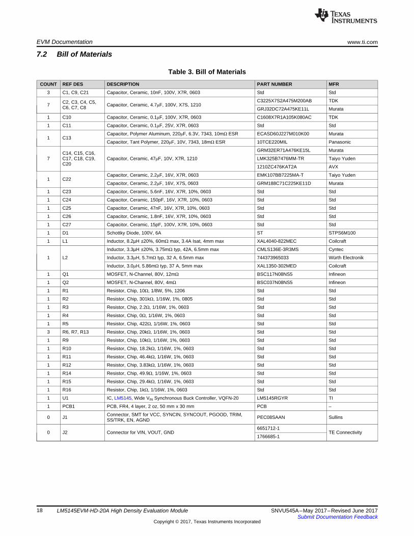
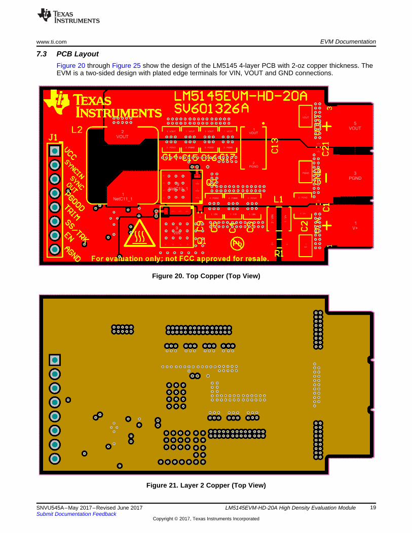
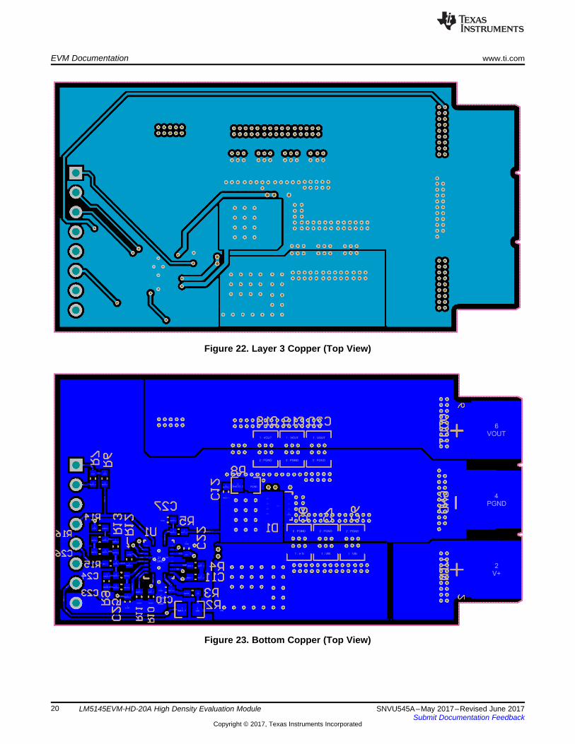
7.3 PCB LayoutFigure 20 through Figure 25 show the design of the LM5145 4-layer PCB with 2-oz copper thickness. TheEVM is a two-sided design with plated edge terminals for VIN, VOUT and GND connections.
Figure 20. Top Copper (Top View)
Figure 21. Layer 2 Copper (Top View)
EVM Documentation www.ti.com
20 SNVU545A–May 2017–Revised June 2017Submit Documentation Feedback
Copyright © 2017, Texas Instruments Incorporated
LM5145EVM-HD-20A High Density Evaluation Module
Figure 22. Layer 3 Copper (Top View)
Figure 23. Bottom Copper (Top View)
www.ti.com EVM Documentation
21SNVU545A–May 2017–Revised June 2017Submit Documentation Feedback
Copyright © 2017, Texas Instruments Incorporated
LM5145EVM-HD-20A High Density Evaluation Module
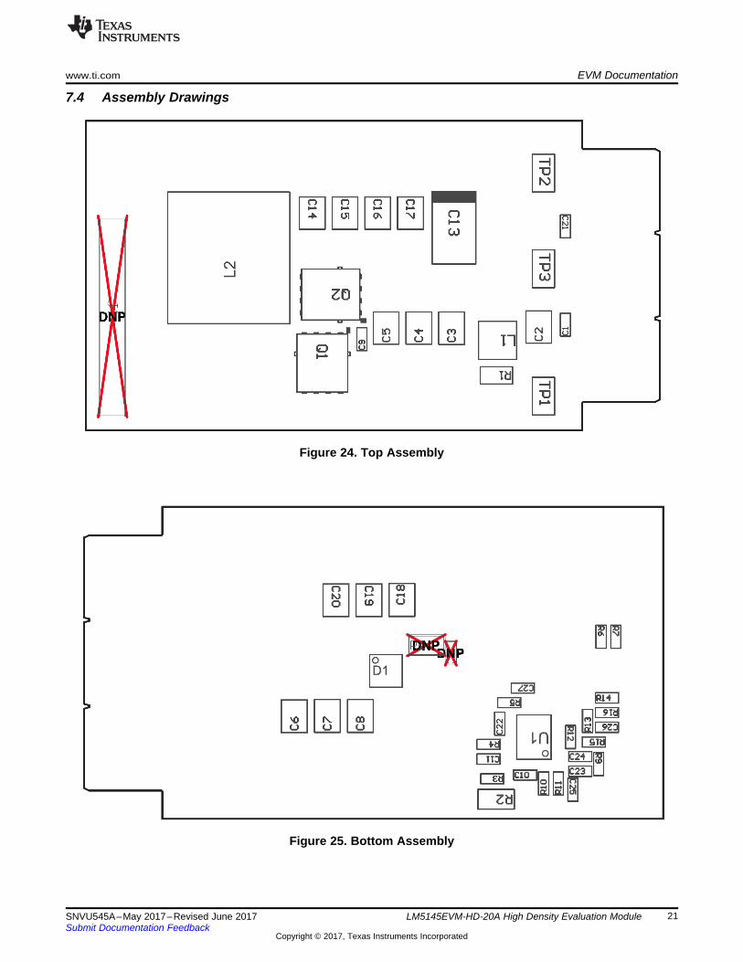
7.4 Assembly Drawings
Figure 24. Top Assembly
Figure 25. Bottom Assembly
Device and Documentation Support www.ti.com
22 SNVU545A–May 2017–Revised June 2017Submit Documentation Feedback
Copyright © 2017, Texas Instruments Incorporated
LM5145EVM-HD-20A High Density Evaluation Module
8 Device and Documentation Support
8.1 Device Support
8.1.1 Third-Party Products DisclaimerTI'S PUBLICATION OF INFORMATION REGARDING THIRD-PARTY PRODUCTS OR SERVICES DOESNOT CONSTITUTE AN ENDORSEMENT REGARDING THE SUITABILITY OF SUCH PRODUCTS ORSERVICES OR A WARRANTY, REPRESENTATION OR ENDORSEMENT OF SUCH PRODUCTS ORSERVICES, EITHER ALONE OR IN COMBINATION WITH ANY TI PRODUCT OR SERVICE.
8.1.2 Development SupportFor development support see the following:• For TI's reference design library, visit TI Designs• For TI's WEBENCH Design Environments, visit the WEBENCH® Design Center• LM5145 DC-DC Controller Quickstart Calculator and PSPICE simulation model
8.2 Documentation Support
8.2.1 Related DocumentationFor related documentation see the following:• AN-1713 LM5116 Evaluation Board (SNVA285)• Reduce Buck Converter EMI and Voltage Stress by Minimizing Inductive Parasitics (SLYT682)• AN-2162 Simple Success with Conducted EMI from DC-DC Converters (SNVA489)• White Papers:
– Valuing Wide VIN, Low EMI Synchronous Buck Circuits for Cost-driven, Demanding Applications(SLYY104)
8.2.1.1 PCB Layout Resources• AN-1149 Layout Guidelines for Switching Power Supplies (SNVA021)• AN-1229 Simple Switcher PCB Layout Guidelines (SNVA054)• Constructing Your Power Supply – Layout Considerations (SLUP230)• Low Radiated EMI Layout Made SIMPLE with LM4360x and LM4600x (SNVA721)• Power House Blogs:
– High-Density PCB Layout of DC-DC Converters
8.2.1.2 Thermal Design Resources• AN-2020 Thermal Design by Insight, Not Hindsight (SNVA419)• AN-1520 A Guide to Board Layout for Best Thermal Resistance for Exposed Pad Packages
(SNVA183)• Semiconductor and IC Package Thermal Metrics (SPRA953)• Thermal Design Made Simple with LM43603 and LM43602 (SNVA719)• PowerPAD Thermally Enhanced Package (SLMA002)• PowerPAD Made Easy (SLMA004)• Using New Thermal Metrics (SBVA025)
www.ti.com Revision History
23SNVU545A–May 2017–Revised June 2017Submit Documentation Feedback
Copyright © 2017, Texas Instruments Incorporated
Revision History
Revision HistoryNOTE: Page numbers for previous revisions may differ from page numbers in the current version.
Changes from Original (May 2017) to A Revision ........................................................................................................... Page
• Added high temp logo, thermal performance plots, and new EVM photo ......................................................... 1
STANDARD TERMS FOR EVALUATION MODULES1. Delivery: TI delivers TI evaluation boards, kits, or modules, including any accompanying demonstration software, components, and/or
documentation which may be provided together or separately (collectively, an “EVM” or “EVMs”) to the User (“User”) in accordancewith the terms set forth herein. User's acceptance of the EVM is expressly subject to the following terms.1.1 EVMs are intended solely for product or software developers for use in a research and development setting to facilitate feasibility
evaluation, experimentation, or scientific analysis of TI semiconductors products. EVMs have no direct function and are notfinished products. EVMs shall not be directly or indirectly assembled as a part or subassembly in any finished product. Forclarification, any software or software tools provided with the EVM (“Software”) shall not be subject to the terms and conditionsset forth herein but rather shall be subject to the applicable terms that accompany such Software
1.2 EVMs are not intended for consumer or household use. EVMs may not be sold, sublicensed, leased, rented, loaned, assigned,or otherwise distributed for commercial purposes by Users, in whole or in part, or used in any finished product or productionsystem.
2 Limited Warranty and Related Remedies/Disclaimers:2.1 These terms do not apply to Software. The warranty, if any, for Software is covered in the applicable Software License
Agreement.2.2 TI warrants that the TI EVM will conform to TI's published specifications for ninety (90) days after the date TI delivers such EVM
to User. Notwithstanding the foregoing, TI shall not be liable for a nonconforming EVM if (a) the nonconformity was caused byneglect, misuse or mistreatment by an entity other than TI, including improper installation or testing, or for any EVMs that havebeen altered or modified in any way by an entity other than TI, (b) the nonconformity resulted from User's design, specificationsor instructions for such EVMs or improper system design, or (c) User has not paid on time. Testing and other quality controltechniques are used to the extent TI deems necessary. TI does not test all parameters of each EVM.User's claims against TI under this Section 2 are void if User fails to notify TI of any apparent defects in the EVMs within ten (10)business days after delivery, or of any hidden defects with ten (10) business days after the defect has been detected.
2.3 TI's sole liability shall be at its option to repair or replace EVMs that fail to conform to the warranty set forth above, or creditUser's account for such EVM. TI's liability under this warranty shall be limited to EVMs that are returned during the warrantyperiod to the address designated by TI and that are determined by TI not to conform to such warranty. If TI elects to repair orreplace such EVM, TI shall have a reasonable time to repair such EVM or provide replacements. Repaired EVMs shall bewarranted for the remainder of the original warranty period. Replaced EVMs shall be warranted for a new full ninety (90) daywarranty period.
3 Regulatory Notices:3.1 United States
3.1.1 Notice applicable to EVMs not FCC-Approved:FCC NOTICE: This kit is designed to allow product developers to evaluate electronic components, circuitry, or softwareassociated with the kit to determine whether to incorporate such items in a finished product and software developers to writesoftware applications for use with the end product. This kit is not a finished product and when assembled may not be resold orotherwise marketed unless all required FCC equipment authorizations are first obtained. Operation is subject to the conditionthat this product not cause harmful interference to licensed radio stations and that this product accept harmful interference.Unless the assembled kit is designed to operate under part 15, part 18 or part 95 of this chapter, the operator of the kit mustoperate under the authority of an FCC license holder or must secure an experimental authorization under part 5 of this chapter.3.1.2 For EVMs annotated as FCC – FEDERAL COMMUNICATIONS COMMISSION Part 15 Compliant:
CAUTIONThis device complies with part 15 of the FCC Rules. Operation is subject to the following two conditions: (1) This device may notcause harmful interference, and (2) this device must accept any interference received, including interference that may causeundesired operation.Changes or modifications not expressly approved by the party responsible for compliance could void the user's authority tooperate the equipment.
FCC Interference Statement for Class A EVM devicesNOTE: This equipment has been tested and found to comply with the limits for a Class A digital device, pursuant to part 15 ofthe FCC Rules. These limits are designed to provide reasonable protection against harmful interference when the equipment isoperated in a commercial environment. This equipment generates, uses, and can radiate radio frequency energy and, if notinstalled and used in accordance with the instruction manual, may cause harmful interference to radio communications.Operation of this equipment in a residential area is likely to cause harmful interference in which case the user will be required tocorrect the interference at his own expense.
FCC Interference Statement for Class B EVM devicesNOTE: This equipment has been tested and found to comply with the limits for a Class B digital device, pursuant to part 15 ofthe FCC Rules. These limits are designed to provide reasonable protection against harmful interference in a residentialinstallation. This equipment generates, uses and can radiate radio frequency energy and, if not installed and used in accordancewith the instructions, may cause harmful interference to radio communications. However, there is no guarantee that interferencewill not occur in a particular installation. If this equipment does cause harmful interference to radio or television reception, whichcan be determined by turning the equipment off and on, the user is encouraged to try to correct the interference by one or moreof the following measures:
• Reorient or relocate the receiving antenna.• Increase the separation between the equipment and receiver.• Connect the equipment into an outlet on a circuit different from that to which the receiver is connected.• Consult the dealer or an experienced radio/TV technician for help.
3.2 Canada3.2.1 For EVMs issued with an Industry Canada Certificate of Conformance to RSS-210 or RSS-247
Concerning EVMs Including Radio Transmitters:This device complies with Industry Canada license-exempt RSSs. Operation is subject to the following two conditions:(1) this device may not cause interference, and (2) this device must accept any interference, including interference that maycause undesired operation of the device.
Concernant les EVMs avec appareils radio:Le présent appareil est conforme aux CNR d'Industrie Canada applicables aux appareils radio exempts de licence. L'exploitationest autorisée aux deux conditions suivantes: (1) l'appareil ne doit pas produire de brouillage, et (2) l'utilisateur de l'appareil doitaccepter tout brouillage radioélectrique subi, même si le brouillage est susceptible d'en compromettre le fonctionnement.
Concerning EVMs Including Detachable Antennas:Under Industry Canada regulations, this radio transmitter may only operate using an antenna of a type and maximum (or lesser)gain approved for the transmitter by Industry Canada. To reduce potential radio interference to other users, the antenna typeand its gain should be so chosen that the equivalent isotropically radiated power (e.i.r.p.) is not more than that necessary forsuccessful communication. This radio transmitter has been approved by Industry Canada to operate with the antenna typeslisted in the user guide with the maximum permissible gain and required antenna impedance for each antenna type indicated.Antenna types not included in this list, having a gain greater than the maximum gain indicated for that type, are strictly prohibitedfor use with this device.
Concernant les EVMs avec antennes détachablesConformément à la réglementation d'Industrie Canada, le présent émetteur radio peut fonctionner avec une antenne d'un type etd'un gain maximal (ou inférieur) approuvé pour l'émetteur par Industrie Canada. Dans le but de réduire les risques de brouillageradioélectrique à l'intention des autres utilisateurs, il faut choisir le type d'antenne et son gain de sorte que la puissance isotroperayonnée équivalente (p.i.r.e.) ne dépasse pas l'intensité nécessaire à l'établissement d'une communication satisfaisante. Leprésent émetteur radio a été approuvé par Industrie Canada pour fonctionner avec les types d'antenne énumérés dans lemanuel d’usage et ayant un gain admissible maximal et l'impédance requise pour chaque type d'antenne. Les types d'antennenon inclus dans cette liste, ou dont le gain est supérieur au gain maximal indiqué, sont strictement interdits pour l'exploitation del'émetteur
3.3 Japan3.3.1 Notice for EVMs delivered in Japan: Please see http://www.tij.co.jp/lsds/ti_ja/general/eStore/notice_01.page 日本国内に
輸入される評価用キット、ボードについては、次のところをご覧ください。http://www.tij.co.jp/lsds/ti_ja/general/eStore/notice_01.page
3.3.2 Notice for Users of EVMs Considered “Radio Frequency Products” in Japan: EVMs entering Japan may not be certifiedby TI as conforming to Technical Regulations of Radio Law of Japan.
If User uses EVMs in Japan, not certified to Technical Regulations of Radio Law of Japan, User is required to follow theinstructions set forth by Radio Law of Japan, which includes, but is not limited to, the instructions below with respect to EVMs(which for the avoidance of doubt are stated strictly for convenience and should be verified by User):1. Use EVMs in a shielded room or any other test facility as defined in the notification #173 issued by Ministry of Internal
Affairs and Communications on March 28, 2006, based on Sub-section 1.1 of Article 6 of the Ministry’s Rule forEnforcement of Radio Law of Japan,
2. Use EVMs only after User obtains the license of Test Radio Station as provided in Radio Law of Japan with respect toEVMs, or
3. Use of EVMs only after User obtains the Technical Regulations Conformity Certification as provided in Radio Law of Japanwith respect to EVMs. Also, do not transfer EVMs, unless User gives the same notice above to the transferee. Please notethat if User does not follow the instructions above, User will be subject to penalties of Radio Law of Japan.
【無線電波を送信する製品の開発キットをお使いになる際の注意事項】 開発キットの中には技術基準適合証明を受けていないものがあります。 技術適合証明を受けていないもののご使用に際しては、電波法遵守のため、以下のいずれかの措置を取っていただく必要がありますのでご注意ください。1. 電波法施行規則第6条第1項第1号に基づく平成18年3月28日総務省告示第173号で定められた電波暗室等の試験設備でご使用
いただく。2. 実験局の免許を取得後ご使用いただく。3. 技術基準適合証明を取得後ご使用いただく。
なお、本製品は、上記の「ご使用にあたっての注意」を譲渡先、移転先に通知しない限り、譲渡、移転できないものとします。上記を遵守頂けない場合は、電波法の罰則が適用される可能性があることをご留意ください。 日本テキサス・イ
ンスツルメンツ株式会社東京都新宿区西新宿6丁目24番1号西新宿三井ビル
3.3.3 Notice for EVMs for Power Line Communication: Please see http://www.tij.co.jp/lsds/ti_ja/general/eStore/notice_02.page電力線搬送波通信についての開発キットをお使いになる際の注意事項については、次のところをご覧ください。http://www.tij.co.jp/lsds/ti_ja/general/eStore/notice_02.page
3.4 European Union3.4.1 For EVMs subject to EU Directive 2014/30/EU (Electromagnetic Compatibility Directive):
This is a class A product intended for use in environments other than domestic environments that are connected to alow-voltage power-supply network that supplies buildings used for domestic purposes. In a domestic environment thisproduct may cause radio interference in which case the user may be required to take adequate measures.
4 EVM Use Restrictions and Warnings:4.1 EVMS ARE NOT FOR USE IN FUNCTIONAL SAFETY AND/OR SAFETY CRITICAL EVALUATIONS, INCLUDING BUT NOT
LIMITED TO EVALUATIONS OF LIFE SUPPORT APPLICATIONS.4.2 User must read and apply the user guide and other available documentation provided by TI regarding the EVM prior to handling
or using the EVM, including without limitation any warning or restriction notices. The notices contain important safety informationrelated to, for example, temperatures and voltages.
4.3 Safety-Related Warnings and Restrictions:4.3.1 User shall operate the EVM within TI’s recommended specifications and environmental considerations stated in the user
guide, other available documentation provided by TI, and any other applicable requirements and employ reasonable andcustomary safeguards. Exceeding the specified performance ratings and specifications (including but not limited to inputand output voltage, current, power, and environmental ranges) for the EVM may cause personal injury or death, orproperty damage. If there are questions concerning performance ratings and specifications, User should contact a TIfield representative prior to connecting interface electronics including input power and intended loads. Any loads appliedoutside of the specified output range may also result in unintended and/or inaccurate operation and/or possiblepermanent damage to the EVM and/or interface electronics. Please consult the EVM user guide prior to connecting anyload to the EVM output. If there is uncertainty as to the load specification, please contact a TI field representative.During normal operation, even with the inputs and outputs kept within the specified allowable ranges, some circuitcomponents may have elevated case temperatures. These components include but are not limited to linear regulators,switching transistors, pass transistors, current sense resistors, and heat sinks, which can be identified using theinformation in the associated documentation. When working with the EVM, please be aware that the EVM may becomevery warm.
4.3.2 EVMs are intended solely for use by technically qualified, professional electronics experts who are familiar with thedangers and application risks associated with handling electrical mechanical components, systems, and subsystems.User assumes all responsibility and liability for proper and safe handling and use of the EVM by User or its employees,affiliates, contractors or designees. User assumes all responsibility and liability to ensure that any interfaces (electronicand/or mechanical) between the EVM and any human body are designed with suitable isolation and means to safelylimit accessible leakage currents to minimize the risk of electrical shock hazard. User assumes all responsibility andliability for any improper or unsafe handling or use of the EVM by User or its employees, affiliates, contractors ordesignees.
4.4 User assumes all responsibility and liability to determine whether the EVM is subject to any applicable international, federal,state, or local laws and regulations related to User’s handling and use of the EVM and, if applicable, User assumes allresponsibility and liability for compliance in all respects with such laws and regulations. User assumes all responsibility andliability for proper disposal and recycling of the EVM consistent with all applicable international, federal, state, and localrequirements.
5. Accuracy of Information: To the extent TI provides information on the availability and function of EVMs, TI attempts to be as accurateas possible. However, TI does not warrant the accuracy of EVM descriptions, EVM availability or other information on its websites asaccurate, complete, reliable, current, or error-free.
6. Disclaimers:6.1 EXCEPT AS SET FORTH ABOVE, EVMS AND ANY MATERIALS PROVIDED WITH THE EVM (INCLUDING, BUT NOT
LIMITED TO, REFERENCE DESIGNS AND THE DESIGN OF THE EVM ITSELF) ARE PROVIDED "AS IS" AND "WITH ALLFAULTS." TI DISCLAIMS ALL OTHER WARRANTIES, EXPRESS OR IMPLIED, REGARDING SUCH ITEMS, INCLUDING BUTNOT LIMITED TO ANY EPIDEMIC FAILURE WARRANTY OR IMPLIED WARRANTIES OF MERCHANTABILITY OR FITNESSFOR A PARTICULAR PURPOSE OR NON-INFRINGEMENT OF ANY THIRD PARTY PATENTS, COPYRIGHTS, TRADESECRETS OR OTHER INTELLECTUAL PROPERTY RIGHTS.
6.2 EXCEPT FOR THE LIMITED RIGHT TO USE THE EVM SET FORTH HEREIN, NOTHING IN THESE TERMS SHALL BECONSTRUED AS GRANTING OR CONFERRING ANY RIGHTS BY LICENSE, PATENT, OR ANY OTHER INDUSTRIAL ORINTELLECTUAL PROPERTY RIGHT OF TI, ITS SUPPLIERS/LICENSORS OR ANY OTHER THIRD PARTY, TO USE THEEVM IN ANY FINISHED END-USER OR READY-TO-USE FINAL PRODUCT, OR FOR ANY INVENTION, DISCOVERY ORIMPROVEMENT, REGARDLESS OF WHEN MADE, CONCEIVED OR ACQUIRED.
7. USER'S INDEMNITY OBLIGATIONS AND REPRESENTATIONS. USER WILL DEFEND, INDEMNIFY AND HOLD TI, ITSLICENSORS AND THEIR REPRESENTATIVES HARMLESS FROM AND AGAINST ANY AND ALL CLAIMS, DAMAGES, LOSSES,EXPENSES, COSTS AND LIABILITIES (COLLECTIVELY, "CLAIMS") ARISING OUT OF OR IN CONNECTION WITH ANYHANDLING OR USE OF THE EVM THAT IS NOT IN ACCORDANCE WITH THESE TERMS. THIS OBLIGATION SHALL APPLYWHETHER CLAIMS ARISE UNDER STATUTE, REGULATION, OR THE LAW OF TORT, CONTRACT OR ANY OTHER LEGALTHEORY, AND EVEN IF THE EVM FAILS TO PERFORM AS DESCRIBED OR EXPECTED.
8. Limitations on Damages and Liability:8.1 General Limitations. IN NO EVENT SHALL TI BE LIABLE FOR ANY SPECIAL, COLLATERAL, INDIRECT, PUNITIVE,
INCIDENTAL, CONSEQUENTIAL, OR EXEMPLARY DAMAGES IN CONNECTION WITH OR ARISING OUT OF THESETERMS OR THE USE OF THE EVMS , REGARDLESS OF WHETHER TI HAS BEEN ADVISED OF THE POSSIBILITY OFSUCH DAMAGES. EXCLUDED DAMAGES INCLUDE, BUT ARE NOT LIMITED TO, COST OF REMOVAL ORREINSTALLATION, ANCILLARY COSTS TO THE PROCUREMENT OF SUBSTITUTE GOODS OR SERVICES, RETESTING,OUTSIDE COMPUTER TIME, LABOR COSTS, LOSS OF GOODWILL, LOSS OF PROFITS, LOSS OF SAVINGS, LOSS OFUSE, LOSS OF DATA, OR BUSINESS INTERRUPTION. NO CLAIM, SUIT OR ACTION SHALL BE BROUGHT AGAINST TIMORE THAN TWELVE (12) MONTHS AFTER THE EVENT THAT GAVE RISE TO THE CAUSE OF ACTION HASOCCURRED.
8.2 Specific Limitations. IN NO EVENT SHALL TI'S AGGREGATE LIABILITY FROM ANY USE OF AN EVM PROVIDEDHEREUNDER, INCLUDING FROM ANY WARRANTY, INDEMITY OR OTHER OBLIGATION ARISING OUT OF OR INCONNECTION WITH THESE TERMS, , EXCEED THE TOTAL AMOUNT PAID TO TI BY USER FOR THE PARTICULAREVM(S) AT ISSUE DURING THE PRIOR TWELVE (12) MONTHS WITH RESPECT TO WHICH LOSSES OR DAMAGES ARECLAIMED. THE EXISTENCE OF MORE THAN ONE CLAIM SHALL NOT ENLARGE OR EXTEND THIS LIMIT.
9. Return Policy. Except as otherwise provided, TI does not offer any refunds, returns, or exchanges. Furthermore, no return of EVM(s)will be accepted if the package has been opened and no return of the EVM(s) will be accepted if they are damaged or otherwise not ina resalable condition. If User feels it has been incorrectly charged for the EVM(s) it ordered or that delivery violates the applicableorder, User should contact TI. All refunds will be made in full within thirty (30) working days from the return of the components(s),excluding any postage or packaging costs.
10. Governing Law: These terms and conditions shall be governed by and interpreted in accordance with the laws of the State of Texas,without reference to conflict-of-laws principles. User agrees that non-exclusive jurisdiction for any dispute arising out of or relating tothese terms and conditions lies within courts located in the State of Texas and consents to venue in Dallas County, Texas.Notwithstanding the foregoing, any judgment may be enforced in any United States or foreign court, and TI may seek injunctive reliefin any United States or foreign court.
Mailing Address: Texas Instruments, Post Office Box 655303, Dallas, Texas 75265Copyright © 2017, Texas Instruments Incorporated

IMPORTANT NOTICE FOR TI DESIGN INFORMATION AND RESOURCES
Texas Instruments Incorporated (‘TI”) technical, application or other design advice, services or information, including, but not limited to,reference designs and materials relating to evaluation modules, (collectively, “TI Resources”) are intended to assist designers who aredeveloping applications that incorporate TI products; by downloading, accessing or using any particular TI Resource in any way, you(individually or, if you are acting on behalf of a company, your company) agree to use it solely for this purpose and subject to the terms ofthis Notice.TI’s provision of TI Resources does not expand or otherwise alter TI’s applicable published warranties or warranty disclaimers for TIproducts, and no additional obligations or liabilities arise from TI providing such TI Resources. TI reserves the right to make corrections,enhancements, improvements and other changes to its TI Resources.You understand and agree that you remain responsible for using your independent analysis, evaluation and judgment in designing yourapplications and that you have full and exclusive responsibility to assure the safety of your applications and compliance of your applications(and of all TI products used in or for your applications) with all applicable regulations, laws and other applicable requirements. Yourepresent that, with respect to your applications, you have all the necessary expertise to create and implement safeguards that (1)anticipate dangerous consequences of failures, (2) monitor failures and their consequences, and (3) lessen the likelihood of failures thatmight cause harm and take appropriate actions. You agree that prior to using or distributing any applications that include TI products, youwill thoroughly test such applications and the functionality of such TI products as used in such applications. TI has not conducted anytesting other than that specifically described in the published documentation for a particular TI Resource.You are authorized to use, copy and modify any individual TI Resource only in connection with the development of applications that includethe TI product(s) identified in such TI Resource. NO OTHER LICENSE, EXPRESS OR IMPLIED, BY ESTOPPEL OR OTHERWISE TOANY OTHER TI INTELLECTUAL PROPERTY RIGHT, AND NO LICENSE TO ANY TECHNOLOGY OR INTELLECTUAL PROPERTYRIGHT OF TI OR ANY THIRD PARTY IS GRANTED HEREIN, including but not limited to any patent right, copyright, mask work right, orother intellectual property right relating to any combination, machine, or process in which TI products or services are used. Informationregarding or referencing third-party products or services does not constitute a license to use such products or services, or a warranty orendorsement thereof. Use of TI Resources may require a license from a third party under the patents or other intellectual property of thethird party, or a license from TI under the patents or other intellectual property of TI.TI RESOURCES ARE PROVIDED “AS IS” AND WITH ALL FAULTS. TI DISCLAIMS ALL OTHER WARRANTIES ORREPRESENTATIONS, EXPRESS OR IMPLIED, REGARDING TI RESOURCES OR USE THEREOF, INCLUDING BUT NOT LIMITED TOACCURACY OR COMPLETENESS, TITLE, ANY EPIDEMIC FAILURE WARRANTY AND ANY IMPLIED WARRANTIES OFMERCHANTABILITY, FITNESS FOR A PARTICULAR PURPOSE, AND NON-INFRINGEMENT OF ANY THIRD PARTY INTELLECTUALPROPERTY RIGHTS.TI SHALL NOT BE LIABLE FOR AND SHALL NOT DEFEND OR INDEMNIFY YOU AGAINST ANY CLAIM, INCLUDING BUT NOTLIMITED TO ANY INFRINGEMENT CLAIM THAT RELATES TO OR IS BASED ON ANY COMBINATION OF PRODUCTS EVEN IFDESCRIBED IN TI RESOURCES OR OTHERWISE. IN NO EVENT SHALL TI BE LIABLE FOR ANY ACTUAL, DIRECT, SPECIAL,COLLATERAL, INDIRECT, PUNITIVE, INCIDENTAL, CONSEQUENTIAL OR EXEMPLARY DAMAGES IN CONNECTION WITH ORARISING OUT OF TI RESOURCES OR USE THEREOF, AND REGARDLESS OF WHETHER TI HAS BEEN ADVISED OF THEPOSSIBILITY OF SUCH DAMAGES.You agree to fully indemnify TI and its representatives against any damages, costs, losses, and/or liabilities arising out of your non-compliance with the terms and provisions of this Notice.This Notice applies to TI Resources. Additional terms apply to the use and purchase of certain types of materials, TI products and services.These include; without limitation, TI’s standard terms for semiconductor products http://www.ti.com/sc/docs/stdterms.htm), evaluationmodules, and samples (http://www.ti.com/sc/docs/sampterms.htm).
Mailing Address: Texas Instruments, Post Office Box 655303, Dallas, Texas 75265Copyright © 2017, Texas Instruments Incorporated