Embed Size (px)
Citation preview
Product
Folder
Sample &Buy
Technical
Documents
Tools &
Software
Support &Community
LM567, LM567CSNOSBQ4E –MAY 1999–REVISED DECEMBER 2014
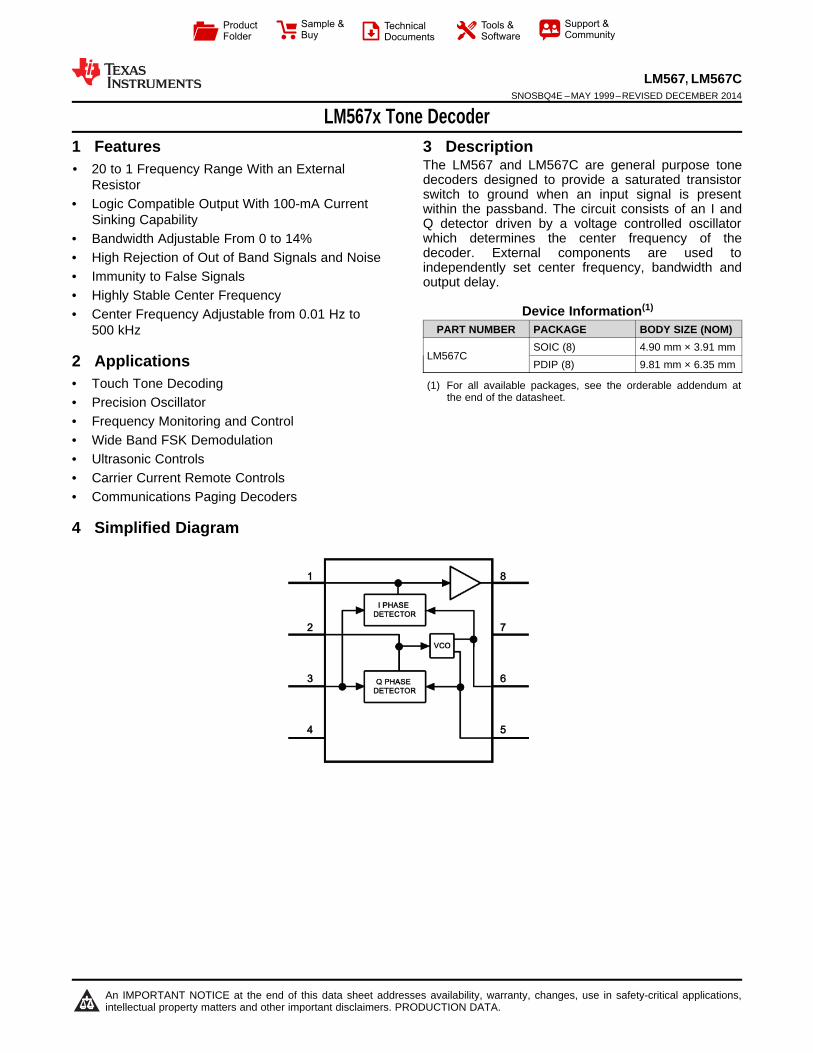
LM567x Tone Decoder1 Features 3 Description
The LM567 and LM567C are general purpose tone1• 20 to 1 Frequency Range With an External
decoders designed to provide a saturated transistorResistorswitch to ground when an input signal is present
• Logic Compatible Output With 100-mA Current within the passband. The circuit consists of an I andSinking Capability Q detector driven by a voltage controlled oscillator
which determines the center frequency of the• Bandwidth Adjustable From 0 to 14%decoder. External components are used to• High Rejection of Out of Band Signals and Noiseindependently set center frequency, bandwidth and
• Immunity to False Signals output delay.• Highly Stable Center Frequency
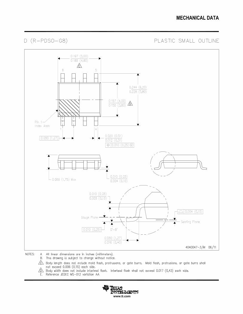
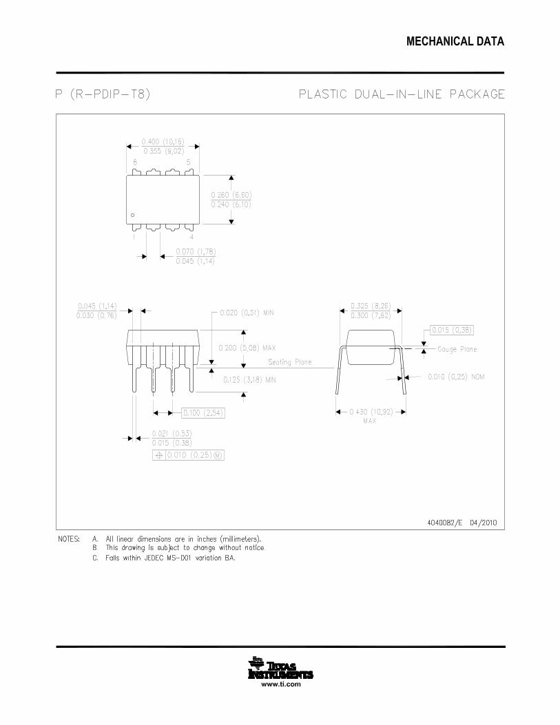
Device Information(1)• Center Frequency Adjustable from 0.01 Hz toPART NUMBER PACKAGE BODY SIZE (NOM)500 kHz
SOIC (8) 4.90 mm × 3.91 mmLM567C2 Applications PDIP (8) 9.81 mm × 6.35 mm
• Touch Tone Decoding (1) For all available packages, see the orderable addendum atthe end of the datasheet.• Precision Oscillator
• Frequency Monitoring and Control• Wide Band FSK Demodulation• Ultrasonic Controls• Carrier Current Remote Controls• Communications Paging Decoders
4 Simplified Diagram
1
An IMPORTANT NOTICE at the end of this data sheet addresses availability, warranty, changes, use in safety-critical applications,intellectual property matters and other important disclaimers. PRODUCTION DATA.
LM567, LM567CSNOSBQ4E –MAY 1999–REVISED DECEMBER 2014 www.ti.com
Table of Contents10.2 Functional Block Diagram ....................................... 81 Features .................................................................. 110.3 Feature Description................................................. 92 Applications ........................................................... 110.4 Device Functional Modes...................................... 103 Description ............................................................. 1
11 Application and Implementation........................ 124 Simplified Diagram ................................................ 111.1 Application Information.......................................... 125 Revision History..................................................... 211.2 Typical Applications .............................................. 136 Device Comparison Table ..................................... 3
12 Power Supply Recommendations ..................... 197 Pin Configuration and Functions ......................... 313 Layout................................................................... 198 Specifications......................................................... 4
13.1 Layout Guidelines ................................................. 198.1 Absolute Maximum Ratings ...................................... 413.2 Layout Example .................................................... 198.2 Recommended Operating Conditions....................... 4
14 Device and Documentation Support ................. 208.3 Thermal Information .................................................. 414.1 Related Links ........................................................ 208.4 Electrical Characteristics........................................... 514.2 Trademarks ........................................................... 208.5 Typical Characteristics .............................................. 614.3 Electrostatic Discharge Caution............................ 209 Parameter Measurement Information .................. 814.4 Glossary ................................................................ 2010 Detailed Description ............................................. 8 15 Mechanical, Packaging, and Orderable10.1 Overview ................................................................. 8 Information ........................................................... 20
5 Revision HistoryNOTE: Page numbers for previous revisions may differ from page numbers in the current version.
Changes from Revision D (March 2013) to Revision E Page
• Added Pin Configuration and Functions section, ESD Ratings table, Feature Description section, Device FunctionalModes, Application and Implementation section, Power Supply Recommendations section, Layout section, Deviceand Documentation Support section, and Mechanical, Packaging, and Orderable Information section .............................. 1
Changes from Revision C (March 2013) to Revision D Page
• Changed layout of National Data Sheet to TI format ............................................................................................................. 9
2 Submit Documentation Feedback Copyright © 1999–2014, Texas Instruments Incorporated
Product Folder Links: LM567 LM567C
LM567, LM567Cwww.ti.com SNOSBQ4E –MAY 1999–REVISED DECEMBER 2014
6 Device Comparison Table
DEVICE NAME DESCRIPTIONLM567, LM567C General Purpose Tone Decoder
LMC567 Same as LM567C, but lower power supply current consumption and double oscillator frequency
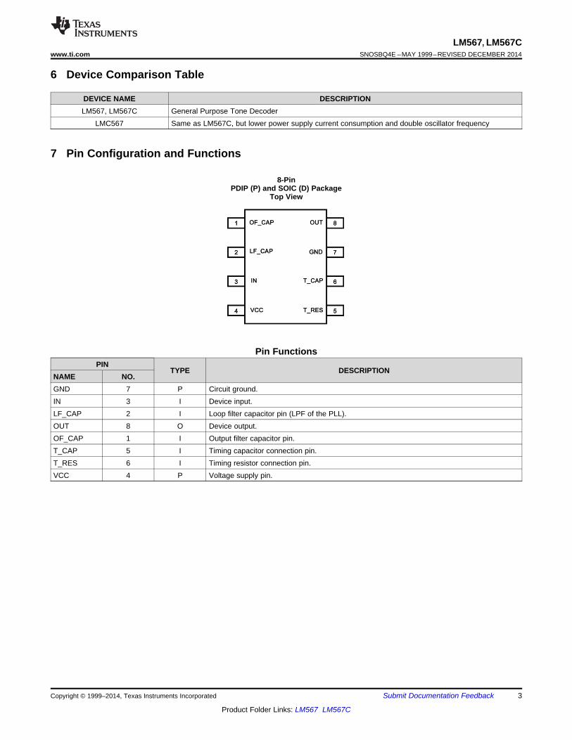
7 Pin Configuration and Functions
8-PinPDIP (P) and SOIC (D) Package
Top View
Pin FunctionsPIN
TYPE DESCRIPTIONNAME NO.GND 7 P Circuit ground.IN 3 I Device input.LF_CAP 2 I Loop filter capacitor pin (LPF of the PLL).OUT 8 O Device output.OF_CAP 1 I Output filter capacitor pin.T_CAP 5 I Timing capacitor connection pin.T_RES 6 I Timing resistor connection pin.VCC 4 P Voltage supply pin.
Copyright © 1999–2014, Texas Instruments Incorporated Submit Documentation Feedback 3
Product Folder Links: LM567 LM567C
LM567, LM567CSNOSBQ4E –MAY 1999–REVISED DECEMBER 2014 www.ti.com
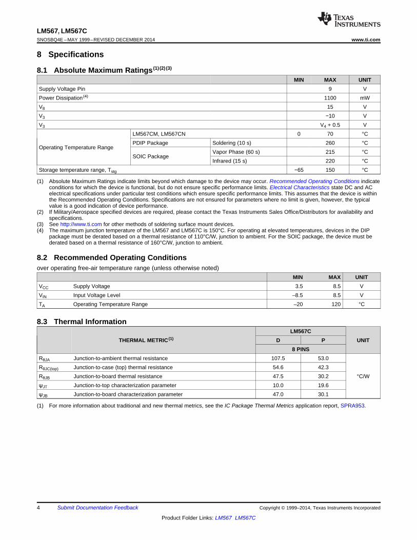
8 Specifications
8.1 Absolute Maximum Ratings (1) (2) (3)
MIN MAX UNITSupply Voltage Pin 9 VPower Dissipation (4) 1100 mWV8 15 VV3 −10 VV3 V4 + 0.5 V
LM567CM, LM567CN 0 70 °CPDIP Package Soldering (10 s) 260 °C
Operating Temperature RangeVapor Phase (60 s) 215 °C
SOIC PackageInfrared (15 s) 220 °C
Storage temperature range, Tstg −65 150 °C
(1) Absolute Maximum Ratings indicate limits beyond which damage to the device may occur. Recommended Operating Conditions indicateconditions for which the device is functional, but do not ensure specific performance limits. Electrical Characteristics state DC and ACelectrical specifications under particular test conditions which ensure specific performance limits. This assumes that the device is withinthe Recommended Operating Conditions. Specifications are not ensured for parameters where no limit is given, however, the typicalvalue is a good indication of device performance.
(2) If Military/Aerospace specified devices are required, please contact the Texas Instruments Sales Office/Distributors for availability andspecifications.
(3) See http://www.ti.com for other methods of soldering surface mount devices.(4) The maximum junction temperature of the LM567 and LM567C is 150°C. For operating at elevated temperatures, devices in the DIP
package must be derated based on a thermal resistance of 110°C/W, junction to ambient. For the SOIC package, the device must bederated based on a thermal resistance of 160°C/W, junction to ambient.
8.2 Recommended Operating Conditionsover operating free-air temperature range (unless otherwise noted)
MIN MAX UNITVCC Supply Voltage 3.5 8.5 VVIN Input Voltage Level –8.5 8.5 VTA Operating Temperature Range –20 120 °C
8.3 Thermal InformationLM567C
THERMAL METRIC (1) D P UNIT8 PINS
RθJA Junction-to-ambient thermal resistance 107.5 53.0RθJC(top) Junction-to-case (top) thermal resistance 54.6 42.3RθJB Junction-to-board thermal resistance 47.5 30.2 °C/WψJT Junction-to-top characterization parameter 10.0 19.6ψJB Junction-to-board characterization parameter 47.0 30.1
(1) For more information about traditional and new thermal metrics, see the IC Package Thermal Metrics application report, SPRA953.
4 Submit Documentation Feedback Copyright © 1999–2014, Texas Instruments Incorporated
Product Folder Links: LM567 LM567C
LM567, LM567Cwww.ti.com SNOSBQ4E –MAY 1999–REVISED DECEMBER 2014
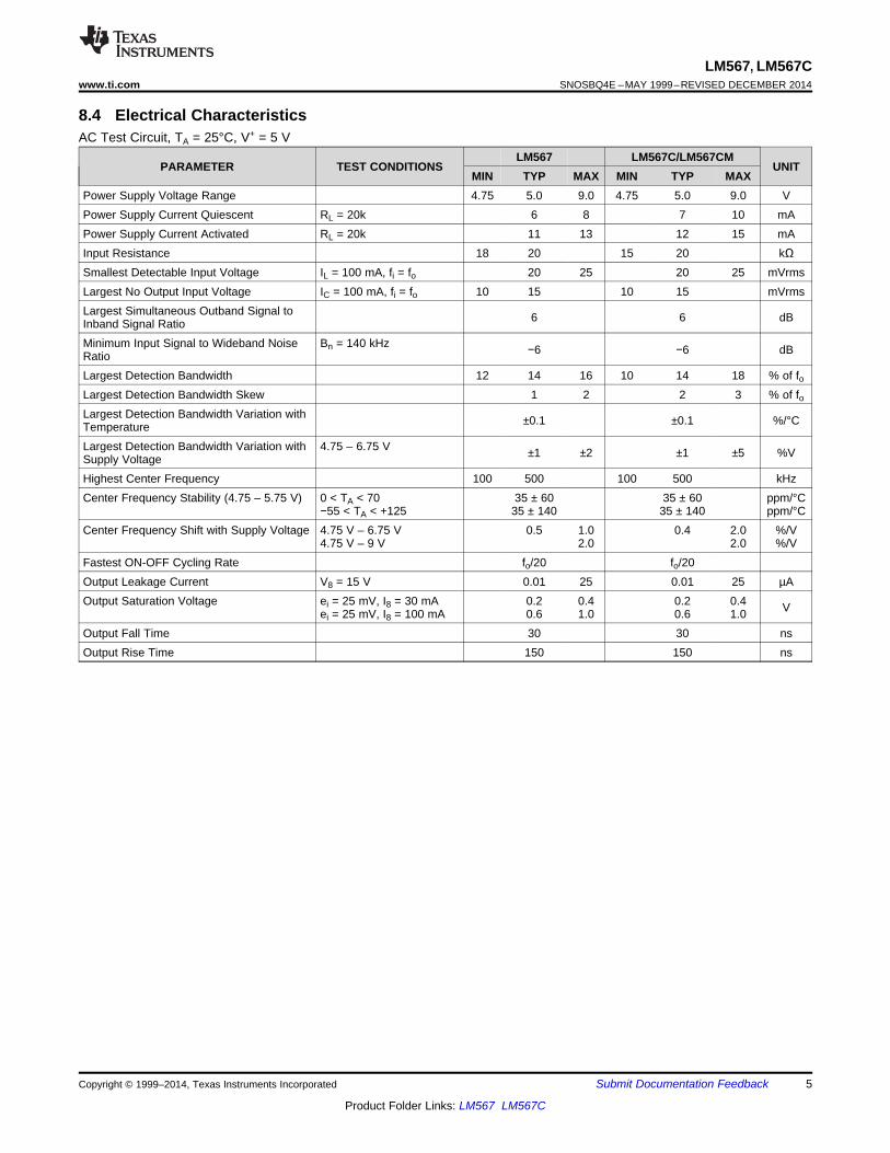
8.4 Electrical CharacteristicsAC Test Circuit, TA = 25°C, V+ = 5 V
LM567 LM567C/LM567CMPARAMETER TEST CONDITIONS UNIT
MIN TYP MAX MIN TYP MAXPower Supply Voltage Range 4.75 5.0 9.0 4.75 5.0 9.0 VPower Supply Current Quiescent RL = 20k 6 8 7 10 mAPower Supply Current Activated RL = 20k 11 13 12 15 mAInput Resistance 18 20 15 20 kΩSmallest Detectable Input Voltage IL = 100 mA, fi = fo 20 25 20 25 mVrmsLargest No Output Input Voltage IC = 100 mA, fi = fo 10 15 10 15 mVrmsLargest Simultaneous Outband Signal to 6 6 dBInband Signal RatioMinimum Input Signal to Wideband Noise Bn = 140 kHz −6 −6 dBRatioLargest Detection Bandwidth 12 14 16 10 14 18 % of foLargest Detection Bandwidth Skew 1 2 2 3 % of foLargest Detection Bandwidth Variation with ±0.1 ±0.1 %/°CTemperatureLargest Detection Bandwidth Variation with 4.75 – 6.75 V ±1 ±2 ±1 ±5 %VSupply VoltageHighest Center Frequency 100 500 100 500 kHzCenter Frequency Stability (4.75 – 5.75 V) 0 < TA < 70 35 ± 60 35 ± 60 ppm/°C
−55 < TA < +125 35 ± 140 35 ± 140 ppm/°CCenter Frequency Shift with Supply Voltage 4.75 V – 6.75 V 0.5 1.0 0.4 2.0 %/V
4.75 V – 9 V 2.0 2.0 %/VFastest ON-OFF Cycling Rate fo/20 fo/20Output Leakage Current V8 = 15 V 0.01 25 0.01 25 µAOutput Saturation Voltage ei = 25 mV, I8 = 30 mA 0.2 0.4 0.2 0.4 Vei = 25 mV, I8 = 100 mA 0.6 1.0 0.6 1.0Output Fall Time 30 30 nsOutput Rise Time 150 150 ns
Copyright © 1999–2014, Texas Instruments Incorporated Submit Documentation Feedback 5
Product Folder Links: LM567 LM567C
LM567, LM567CSNOSBQ4E –MAY 1999–REVISED DECEMBER 2014 www.ti.com
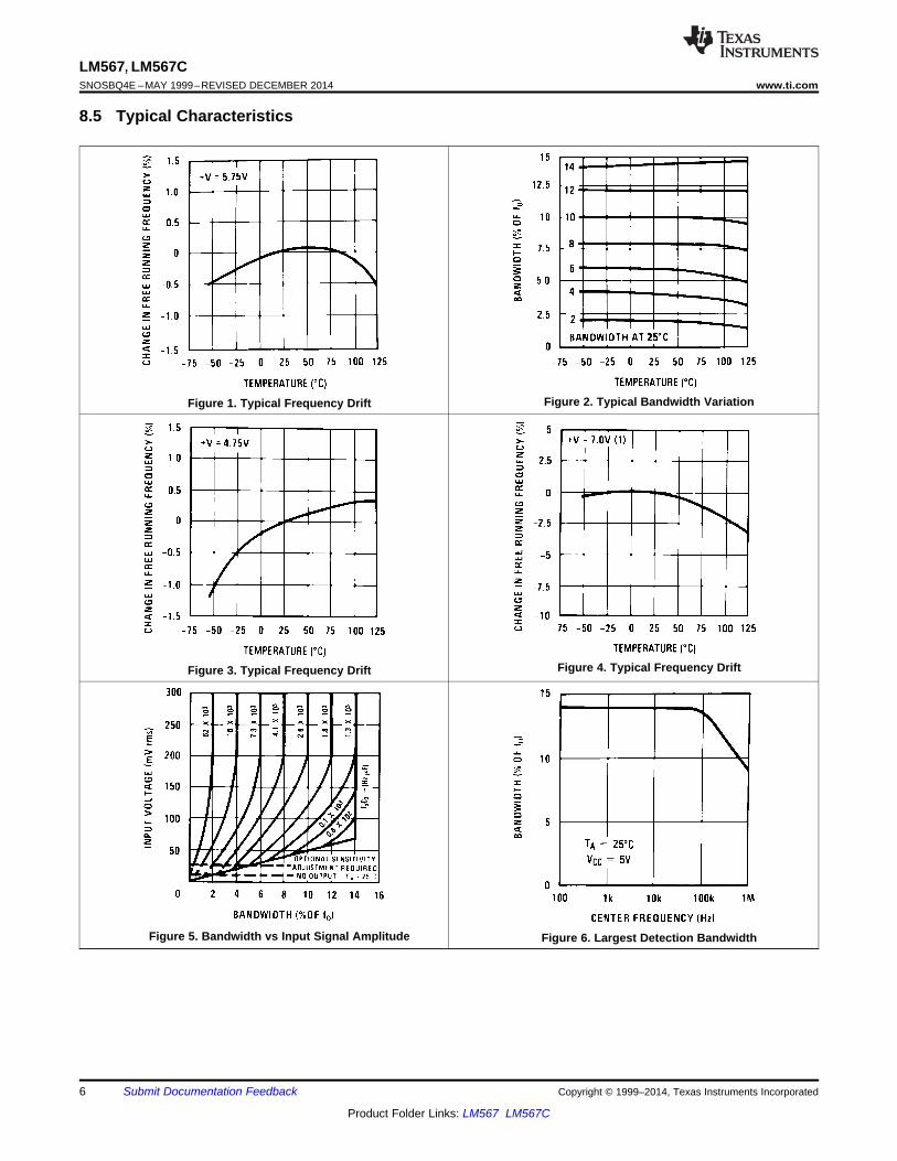
8.5 Typical Characteristics
Figure 2. Typical Bandwidth VariationFigure 1. Typical Frequency Drift
Figure 4. Typical Frequency DriftFigure 3. Typical Frequency Drift
Figure 5. Bandwidth vs Input Signal Amplitude Figure 6. Largest Detection Bandwidth
6 Submit Documentation Feedback Copyright © 1999–2014, Texas Instruments Incorporated
Product Folder Links: LM567 LM567C
LM567, LM567Cwww.ti.com SNOSBQ4E –MAY 1999–REVISED DECEMBER 2014
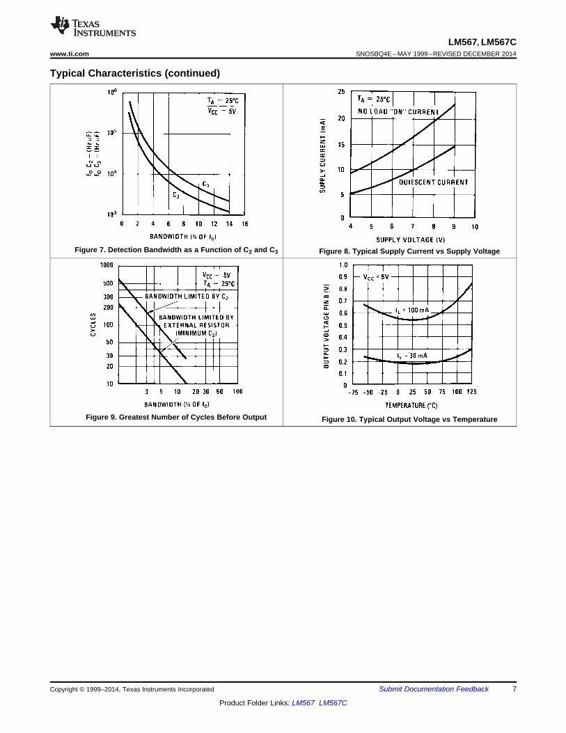
Typical Characteristics (continued)
Figure 7. Detection Bandwidth as a Function of C2 and C3 Figure 8. Typical Supply Current vs Supply Voltage
Figure 9. Greatest Number of Cycles Before Output Figure 10. Typical Output Voltage vs Temperature
Copyright © 1999–2014, Texas Instruments Incorporated Submit Documentation Feedback 7
Product Folder Links: LM567 LM567C
LM567, LM567CSNOSBQ4E –MAY 1999–REVISED DECEMBER 2014 www.ti.com
9 Parameter Measurement Information
All parameters are measured according to the conditions described in the Specifications section.
10 Detailed Description
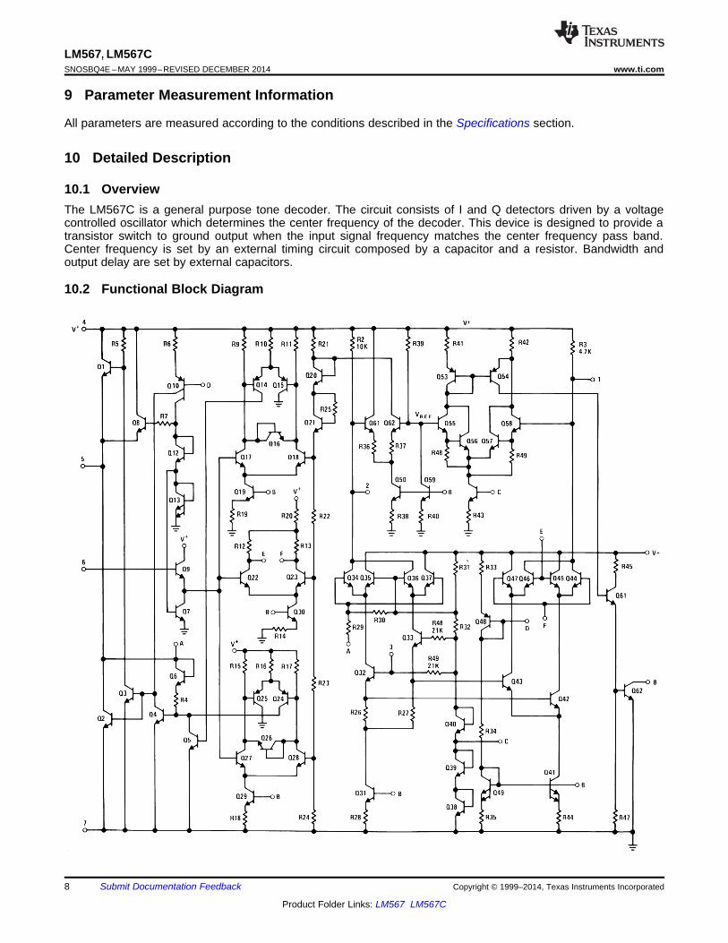
10.1 OverviewThe LM567C is a general purpose tone decoder. The circuit consists of I and Q detectors driven by a voltagecontrolled oscillator which determines the center frequency of the decoder. This device is designed to provide atransistor switch to ground output when the input signal frequency matches the center frequency pass band.Center frequency is set by an external timing circuit composed by a capacitor and a resistor. Bandwidth andoutput delay are set by external capacitors.
10.2 Functional Block Diagram
8 Submit Documentation Feedback Copyright © 1999–2014, Texas Instruments Incorporated
Product Folder Links: LM567 LM567C
o
1 1
1.1f
R C»
LM567, LM567Cwww.ti.com SNOSBQ4E –MAY 1999–REVISED DECEMBER 2014
10.3 Feature Description
10.3.1 Center FrequencyThe center frequency of the LM567 tone decoder is equal to the free running frequency of the voltage controlledoscillator. In order to set this frequency, external components should be placed externally. The componentvalues are given by:
where• R1 = Timing Resistor• C1 = Timing Capacitor (1)
10.3.2 Output FilterTo eliminate undesired signals that could trigger the output stage, a post detection filter is featured in theLM567C. This filter consists of an internal resistor (4.7K-Ω) and an external capacitor. Although typically externalcapacitor value is not critical, it is recommended to be at least twice the value of the loop filter capacitor. If theoutput filter capacitor value is too large, the turn-on and turn off-time of the output will present a delay until thevoltage across this capacitor reaches the threshold level.
10.3.3 Loop FilterThe phase locked loop (PLL) included in the LM567 has a pin for connecting the low pass loop filter capacitor.The selection of the capacitor for the filter depends on the desired bandwidth. The device bandwidth selection isdifferent according to the input voltage level. Refer to the Operation With Vi < 200m – VRMS section and theOperation With Vi > 200m – VRMS section for more information about the loop filter capacitor selection.
10.3.4 Logic OutputThe LM567 is designed to provide a transistor switch to ground output when the input signal frequency matchesthe center frequency pass band. The logic output is an open collector power transistor that requires an externalload resistor that is used to regulate the output current level.
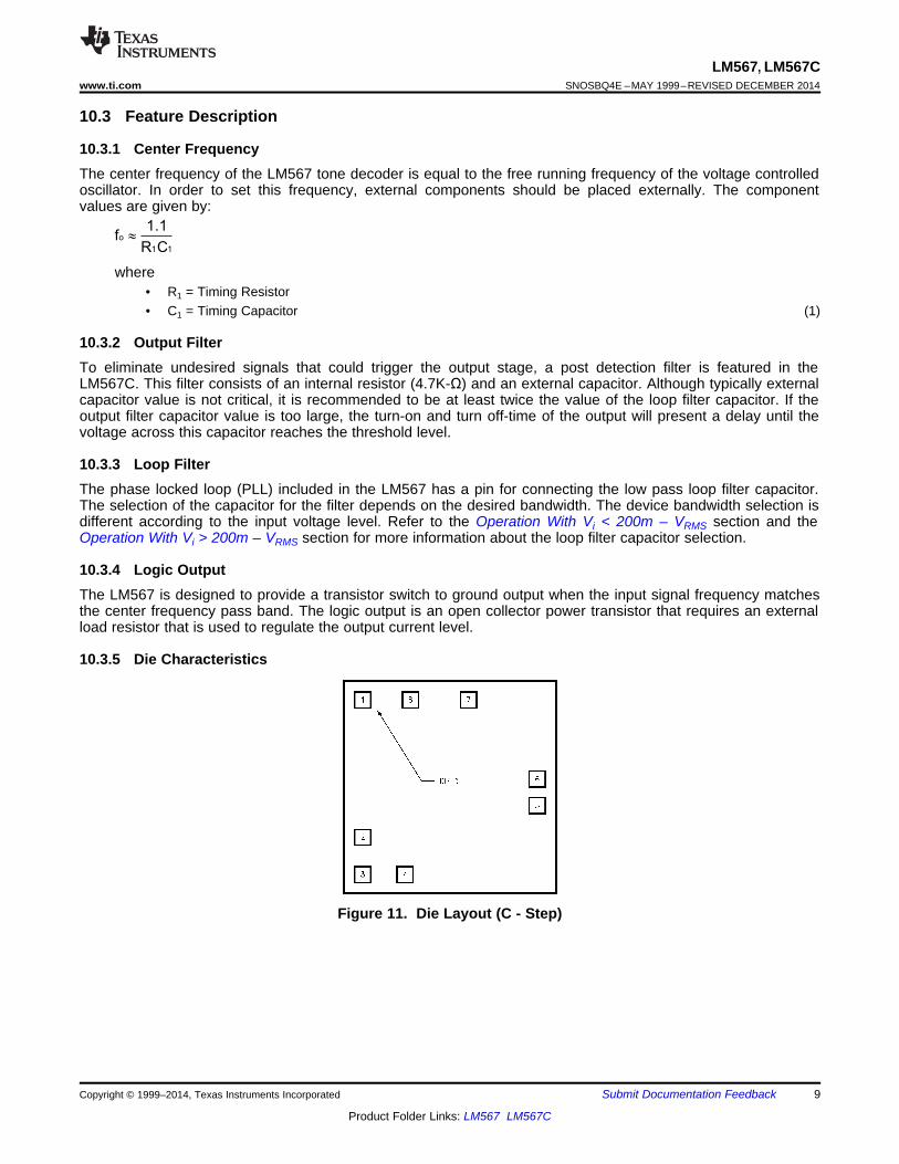
10.3.5 Die Characteristics
Figure 11. Die Layout (C - Step)
Copyright © 1999–2014, Texas Instruments Incorporated Submit Documentation Feedback 9
Product Folder Links: LM567 LM567C
LM567, LM567CSNOSBQ4E –MAY 1999–REVISED DECEMBER 2014 www.ti.com
Feature Description (continued)Table 1. Die and Wafer Characteristics
Fabrication Attributes General Die InformationPhysical Die Identification LM567C Bond Pad Opening Size (min) 91µm x 91µmDie Step C Bond Pad Metalization 0.5% COPPER_BAL.
ALUMINUMPhysical Attributes Passivation VOM NITRIDE
Wafer Diameter 150mm Back Side Metal BARE BACKDise Size (Drawn) 1600µm x 1626µm Back Side Connection Floating
63.0mils x 64.0milsThickness 406µm NominalMin Pitch 198µm NominalSpecial Assembly Requirements:Note: Actual die size is rounded to the nearest micron.
Die Bond Pad Coordinate Locations (C - Step)(Referenced to die center, coordinates in µm) NC = No Connection, N.U. = Not Used
X/Y COORDINATES PAD SIZESIGNAL NAME PAD# NUMBER
X Y X YOUTPUT FILTER 1 -673 686 91 x 91LOOP FILTER 2 -673 -419 91 x 91INPUT 3 -673 -686 91 x 91V+ 4 -356 -686 91 x 91TIMING RES 5 673 -122 91 x 91TIMING CAP 6 673 76 91 x 91GND 7 178 686 117 x 91OUTPUT 8 -318 679 117 x 104
10.4 Device Functional Modes
10.4.1 Operation With Vi < 200m – VRMS
When the input signal is below a threshold voltage, typically 200m-VRMS, the bandwidth of the detection bandshould be calculated .
where• Vi = Input voltage (volts rms), Vi ≤ 200mV• C2 = Capacitance at Pin 2(μF)
10 Submit Documentation Feedback Copyright © 1999–2014, Texas Instruments Incorporated
Product Folder Links: LM567 LM567C
LM567, LM567Cwww.ti.com SNOSBQ4E –MAY 1999–REVISED DECEMBER 2014
Device Functional Modes (continued)10.4.2 Operation With Vi > 200m – VRMS
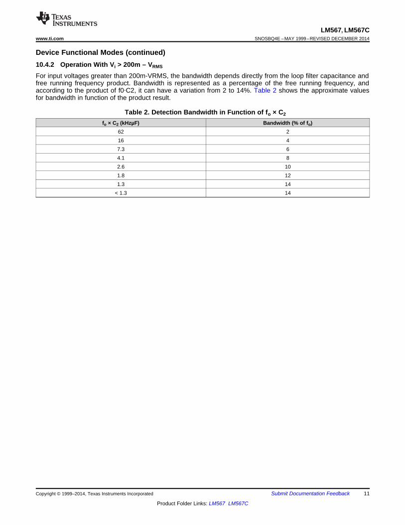
For input voltages greater than 200m-VRMS, the bandwidth depends directly from the loop filter capacitance andfree running frequency product. Bandwidth is represented as a percentage of the free running frequency, andaccording to the product of f0∙C2, it can have a variation from 2 to 14%. Table 2 shows the approximate valuesfor bandwidth in function of the product result.
Table 2. Detection Bandwidth in Function of fo × C2
fo × C2 (kHzµF) Bandwidth (% of fo)62 216 47.3 64.1 82.6 101.8 121.3 14
< 1.3 14
Copyright © 1999–2014, Texas Instruments Incorporated Submit Documentation Feedback 11
Product Folder Links: LM567 LM567C
LM567, LM567CSNOSBQ4E –MAY 1999–REVISED DECEMBER 2014 www.ti.com
11 Application and Implementation
NOTEInformation in the following applications sections is not part of the TI componentspecification, and TI does not warrant its accuracy or completeness. TI’s customers areresponsible for determining suitability of components for their purposes. Customers shouldvalidate and test their design implementation to confirm system functionality.
11.1 Application InformationThe LM567 tone decoder is a device capable of detecting if an input signal is inside a selectable range ofdetection. The device has an open collector transistor output, so an external resistor is required to achieveproper logic levels. When the input signal is inside the detection band, the device output will go to a LOW state.The internal VCO free running frequency establishes the detection band central frequency. An external RC filteris required to set this frequency. The bandwidth in which the device will detect the desired frequency depends onthe capacitance of loop filter terminal. Typically a 1µF capacitor is connected to this pin. The device detectionband has a different behavior for low and high input voltage levels. Refer to the Operation With Vi < 200m – VRMSsection and the Operation With Vi > 200m – VRMS section for more information.
12 Submit Documentation Feedback Copyright © 1999–2014, Texas Instruments Incorporated
Product Folder Links: LM567 LM567C
LM567, LM567Cwww.ti.com SNOSBQ4E –MAY 1999–REVISED DECEMBER 2014
11.2 Typical Applications
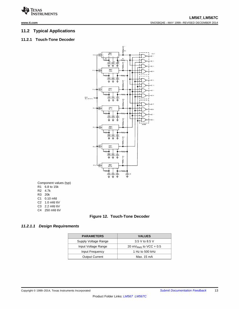
11.2.1 Touch-Tone Decoder
Component values (typ)R1 6.8 to 15kR2 4.7kR3 20kC1 0.10 mfdC2 1.0 mfd 6VC3 2.2 mfd 6VC4 250 mfd 6V
Figure 12. Touch-Tone Decoder
11.2.1.1 Design Requirements
PARAMETERS VALUESSupply Voltage Range 3.5 V to 8.5 VInput Voltage Range 20 mVRMS to VCC + 0.5
Input Frequency 1 Hz to 500 kHzOutput Current Max. 15 mA
Copyright © 1999–2014, Texas Instruments Incorporated Submit Documentation Feedback 13
Product Folder Links: LM567 LM567C
IN (PIN 3)OUT (PIN 8)
o
1 1
1.1f
R C»
LM567, LM567CSNOSBQ4E –MAY 1999–REVISED DECEMBER 2014 www.ti.com
11.2.1.2 Detailed Design Procedure
11.2.1.2.1 Timing Components
To calculate the timing components for an approximated desired central detection frequency (f0), the timingcapacitor value (C1) should be stated in order to calculate the timing resistor value (R1). Typically for mostapplications, a 0.1-µF capacitor is used.
(2)
11.2.1.2.2 Bandwidth
Detection bandwidth is represented as a percentage of f0. It can be selected based on the input voltage levels(Vi). For Vi < 200 mVRMS,
(3)
For Vi > 200 mVRMS, refer to Table 2 or Figure 5.
11.2.1.2.3 Output Filter
The output filter selection is made considering the capacitor value to be at least twice the Loop filter capacitor.C3 ≥ 2C2 (4)
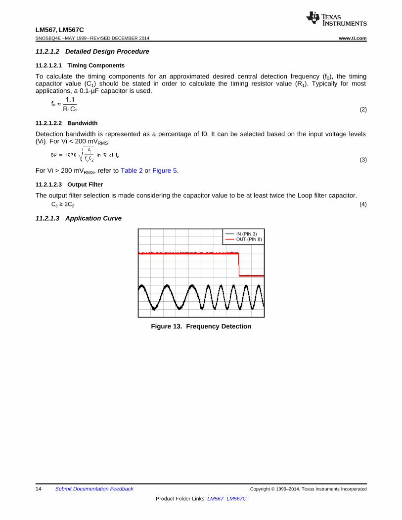
11.2.1.3 Application Curve
Figure 13. Frequency Detection
14 Submit Documentation Feedback Copyright © 1999–2014, Texas Instruments Incorporated
Product Folder Links: LM567 LM567C
OUT 1 (PIN 3)OUT 2 (PIN 8)
LM567, LM567Cwww.ti.com SNOSBQ4E –MAY 1999–REVISED DECEMBER 2014
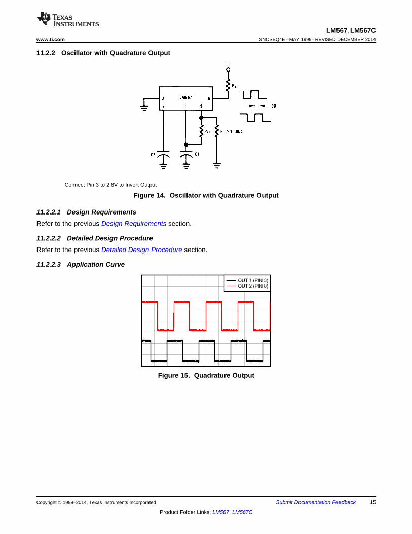
11.2.2 Oscillator with Quadrature Output
Connect Pin 3 to 2.8V to Invert Output
Figure 14. Oscillator with Quadrature Output
11.2.2.1 Design RequirementsRefer to the previous Design Requirements section.
11.2.2.2 Detailed Design ProcedureRefer to the previous Detailed Design Procedure section.
11.2.2.3 Application Curve
Figure 15. Quadrature Output
Copyright © 1999–2014, Texas Instruments Incorporated Submit Documentation Feedback 15
Product Folder Links: LM567 LM567C
OUT 1 (PIN 5)OUT 2 (PIN 8)
LM567, LM567CSNOSBQ4E –MAY 1999–REVISED DECEMBER 2014 www.ti.com
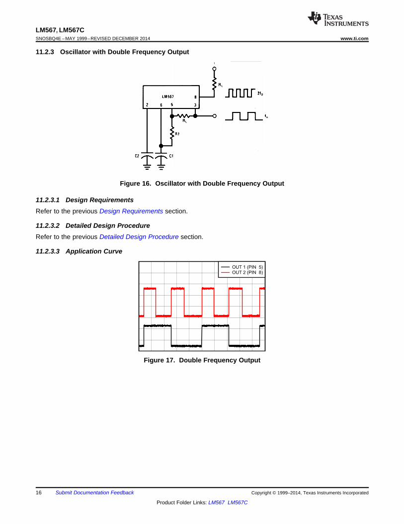
11.2.3 Oscillator with Double Frequency Output
Figure 16. Oscillator with Double Frequency Output
11.2.3.1 Design RequirementsRefer to the previous Design Requirements section.
11.2.3.2 Detailed Design ProcedureRefer to the previous Detailed Design Procedure section.
11.2.3.3 Application Curve
Figure 17. Double Frequency Output
16 Submit Documentation Feedback Copyright © 1999–2014, Texas Instruments Incorporated
Product Folder Links: LM567 LM567C
OUT (PIN 8)
LM567, LM567Cwww.ti.com SNOSBQ4E –MAY 1999–REVISED DECEMBER 2014
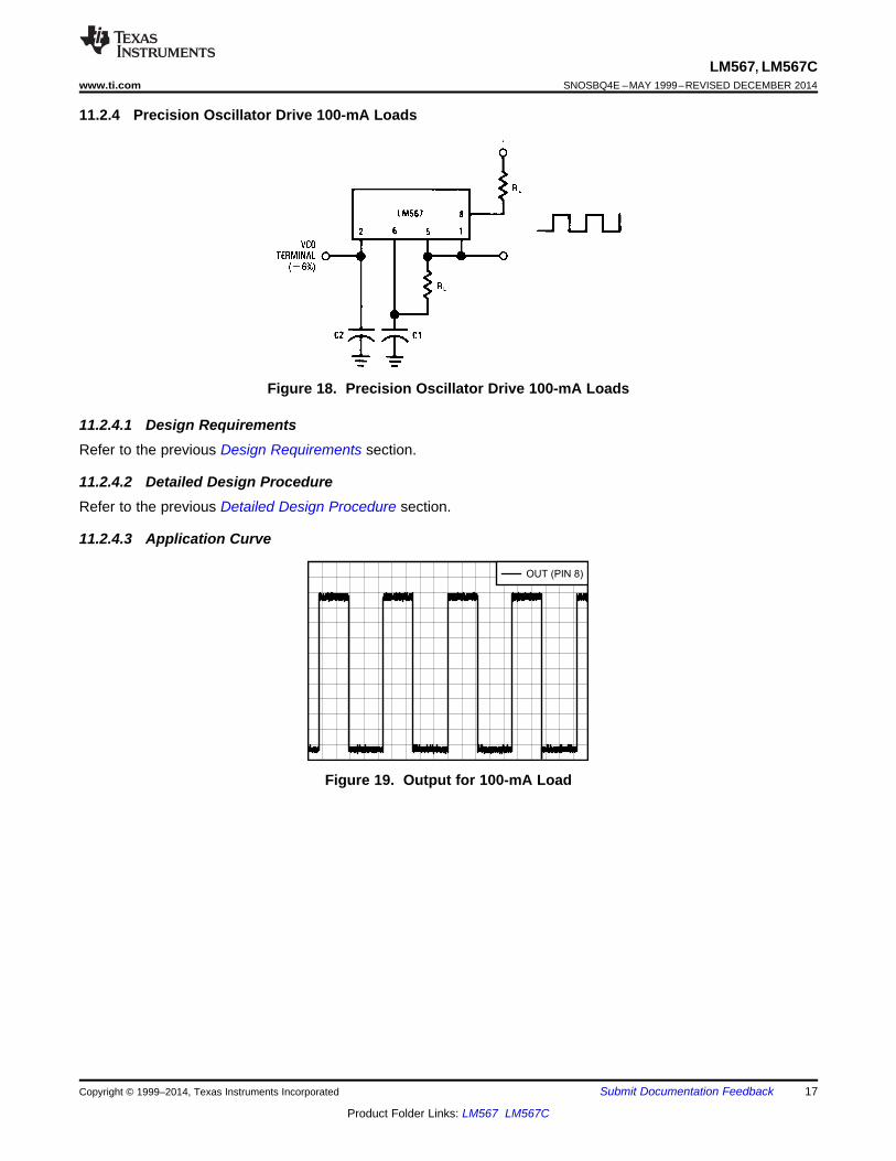
11.2.4 Precision Oscillator Drive 100-mA Loads
Figure 18. Precision Oscillator Drive 100-mA Loads
11.2.4.1 Design RequirementsRefer to the previous Design Requirements section.
11.2.4.2 Detailed Design ProcedureRefer to the previous Detailed Design Procedure section.
11.2.4.3 Application Curve
Figure 19. Output for 100-mA Load
Copyright © 1999–2014, Texas Instruments Incorporated Submit Documentation Feedback 17
Product Folder Links: LM567 LM567C
LM567, LM567CSNOSBQ4E –MAY 1999–REVISED DECEMBER 2014 www.ti.com
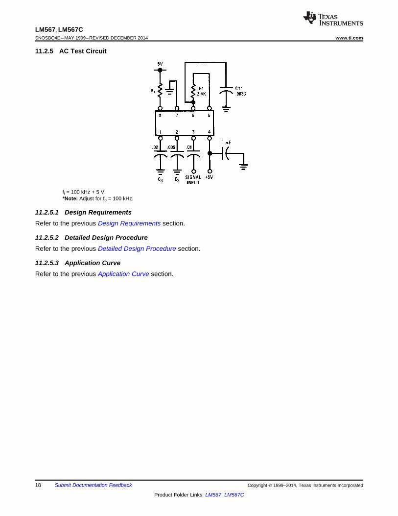
11.2.5 AC Test Circuit
fi = 100 kHz + 5 V*Note: Adjust for fo = 100 kHz.
11.2.5.1 Design RequirementsRefer to the previous Design Requirements section.
11.2.5.2 Detailed Design ProcedureRefer to the previous Detailed Design Procedure section.
11.2.5.3 Application CurveRefer to the previous Application Curve section.
18 Submit Documentation Feedback Copyright © 1999–2014, Texas Instruments Incorporated
Product Folder Links: LM567 LM567C
LM567, LM567Cwww.ti.com SNOSBQ4E –MAY 1999–REVISED DECEMBER 2014
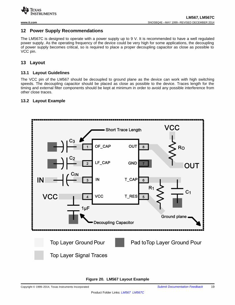
12 Power Supply RecommendationsThe LM567C is designed to operate with a power supply up to 9 V. It is recommended to have a well regulatedpower supply. As the operating frequency of the device could be very high for some applications, the decouplingof power supply becomes critical, so is required to place a proper decoupling capacitor as close as possible toVCC pin.
13 Layout
13.1 Layout GuidelinesThe VCC pin of the LM567 should be decoupled to ground plane as the device can work with high switchingspeeds. The decoupling capacitor should be placed as close as possible to the device. Traces length for thetiming and external filter components should be kept at minimum in order to avoid any possible interference fromother close traces.
13.2 Layout Example
Figure 20. LM567 Layout Example
Copyright © 1999–2014, Texas Instruments Incorporated Submit Documentation Feedback 19
Product Folder Links: LM567 LM567C
LM567, LM567CSNOSBQ4E –MAY 1999–REVISED DECEMBER 2014 www.ti.com
14 Device and Documentation Support
14.1 Related LinksThe table below lists quick access links. Categories include technical documents, support and communityresources, tools and software, and quick access to sample or buy.
Table 3. Related LinksTECHNICAL TOOLS & SUPPORT &PARTS PRODUCT FOLDER SAMPLE & BUY DOCUMENTS SOFTWARE COMMUNITY
LM567 Click here Click here Click here Click here Click hereLM567C Click here Click here Click here Click here Click here
14.2 TrademarksAll trademarks are the property of their respective owners.
14.3 Electrostatic Discharge CautionThese devices have limited built-in ESD protection. The leads should be shorted together or the device placed in conductive foamduring storage or handling to prevent electrostatic damage to the MOS gates.
14.4 GlossarySLYZ022 — TI Glossary.
This glossary lists and explains terms, acronyms, and definitions.
15 Mechanical, Packaging, and Orderable InformationThe following pages include mechanical, packaging, and orderable information. This information is the mostcurrent data available for the designated devices. This data is subject to change without notice and revision ofthis document. For browser-based versions of this data sheet, refer to the left-hand navigation.
20 Submit Documentation Feedback Copyright © 1999–2014, Texas Instruments Incorporated
Product Folder Links: LM567 LM567C
PACKAGE OPTION ADDENDUM
www.ti.com 14-Nov-2017
Addendum-Page 1
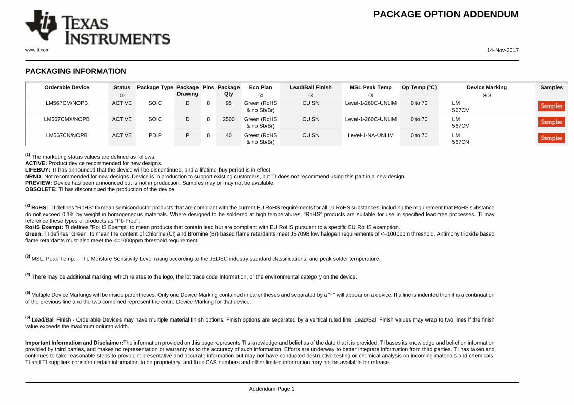
PACKAGING INFORMATION
Orderable Device Status(1)
Package Type PackageDrawing
Pins PackageQty
Eco Plan(2)
Lead/Ball Finish(6)
MSL Peak Temp(3)
Op Temp (°C) Device Marking(4/5)
Samples
LM567CM/NOPB ACTIVE SOIC D 8 95 Green (RoHS& no Sb/Br)
CU SN Level-1-260C-UNLIM 0 to 70 LM567CM
LM567CMX/NOPB ACTIVE SOIC D 8 2500 Green (RoHS& no Sb/Br)
CU SN Level-1-260C-UNLIM 0 to 70 LM567CM
LM567CN/NOPB ACTIVE PDIP P 8 40 Green (RoHS& no Sb/Br)
CU SN Level-1-NA-UNLIM 0 to 70 LM567CN
(1) The marketing status values are defined as follows:ACTIVE: Product device recommended for new designs.LIFEBUY: TI has announced that the device will be discontinued, and a lifetime-buy period is in effect.NRND: Not recommended for new designs. Device is in production to support existing customers, but TI does not recommend using this part in a new design.PREVIEW: Device has been announced but is not in production. Samples may or may not be available.OBSOLETE: TI has discontinued the production of the device.
(2) RoHS: TI defines "RoHS" to mean semiconductor products that are compliant with the current EU RoHS requirements for all 10 RoHS substances, including the requirement that RoHS substancedo not exceed 0.1% by weight in homogeneous materials. Where designed to be soldered at high temperatures, "RoHS" products are suitable for use in specified lead-free processes. TI mayreference these types of products as "Pb-Free".RoHS Exempt: TI defines "RoHS Exempt" to mean products that contain lead but are compliant with EU RoHS pursuant to a specific EU RoHS exemption.Green: TI defines "Green" to mean the content of Chlorine (Cl) and Bromine (Br) based flame retardants meet JS709B low halogen requirements of <=1000ppm threshold. Antimony trioxide basedflame retardants must also meet the <=1000ppm threshold requirement.
(3) MSL, Peak Temp. - The Moisture Sensitivity Level rating according to the JEDEC industry standard classifications, and peak solder temperature.
(4) There may be additional marking, which relates to the logo, the lot trace code information, or the environmental category on the device.
(5) Multiple Device Markings will be inside parentheses. Only one Device Marking contained in parentheses and separated by a "~" will appear on a device. If a line is indented then it is a continuationof the previous line and the two combined represent the entire Device Marking for that device.
(6) Lead/Ball Finish - Orderable Devices may have multiple material finish options. Finish options are separated by a vertical ruled line. Lead/Ball Finish values may wrap to two lines if the finishvalue exceeds the maximum column width.
Important Information and Disclaimer:The information provided on this page represents TI's knowledge and belief as of the date that it is provided. TI bases its knowledge and belief on informationprovided by third parties, and makes no representation or warranty as to the accuracy of such information. Efforts are underway to better integrate information from third parties. TI has taken andcontinues to take reasonable steps to provide representative and accurate information but may not have conducted destructive testing or chemical analysis on incoming materials and chemicals.TI and TI suppliers consider certain information to be proprietary, and thus CAS numbers and other limited information may not be available for release.
PACKAGE OPTION ADDENDUM
www.ti.com 14-Nov-2017
Addendum-Page 2
In no event shall TI's liability arising out of such information exceed the total purchase price of the TI part(s) at issue in this document sold by TI to Customer on an annual basis.
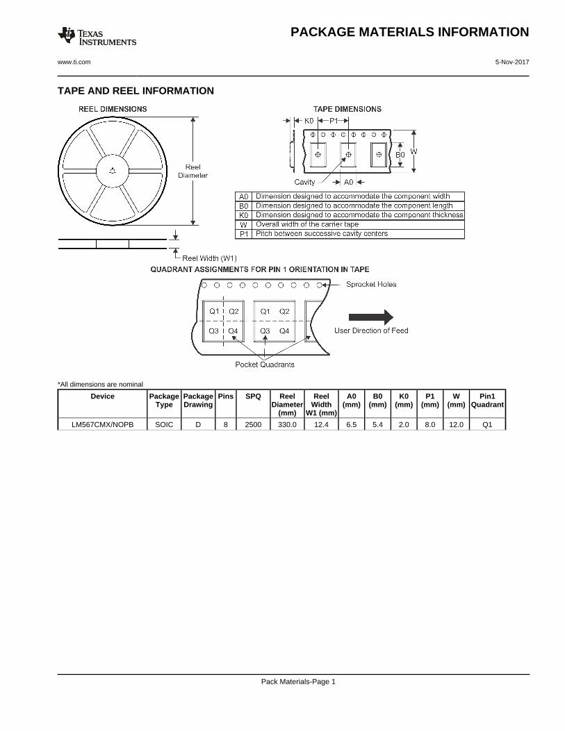
TAPE AND REEL INFORMATION
*All dimensions are nominal
Device PackageType
PackageDrawing
Pins SPQ ReelDiameter
(mm)
ReelWidth
W1 (mm)
A0(mm)
B0(mm)
K0(mm)
P1(mm)
W(mm)
Pin1Quadrant
LM567CMX/NOPB SOIC D 8 2500 330.0 12.4 6.5 5.4 2.0 8.0 12.0 Q1
PACKAGE MATERIALS INFORMATION
www.ti.com 5-Nov-2017
Pack Materials-Page 1
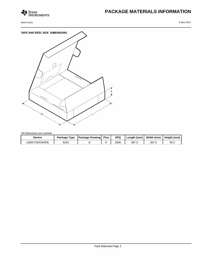
*All dimensions are nominal
Device Package Type Package Drawing Pins SPQ Length (mm) Width (mm) Height (mm)
LM567CMX/NOPB SOIC D 8 2500 367.0 367.0 35.0
PACKAGE MATERIALS INFORMATION
www.ti.com 5-Nov-2017
Pack Materials-Page 2
IMPORTANT NOTICE
Texas Instruments Incorporated (TI) reserves the right to make corrections, enhancements, improvements and other changes to itssemiconductor products and services per JESD46, latest issue, and to discontinue any product or service per JESD48, latest issue. Buyersshould obtain the latest relevant information before placing orders and should verify that such information is current and complete.TI’s published terms of sale for semiconductor products (http://www.ti.com/sc/docs/stdterms.htm) apply to the sale of packaged integratedcircuit products that TI has qualified and released to market. Additional terms may apply to the use or sale of other types of TI products andservices.Reproduction of significant portions of TI information in TI data sheets is permissible only if reproduction is without alteration and isaccompanied by all associated warranties, conditions, limitations, and notices. TI is not responsible or liable for such reproduceddocumentation. Information of third parties may be subject to additional restrictions. Resale of TI products or services with statementsdifferent from or beyond the parameters stated by TI for that product or service voids all express and any implied warranties for theassociated TI product or service and is an unfair and deceptive business practice. TI is not responsible or liable for any such statements.Buyers and others who are developing systems that incorporate TI products (collectively, “Designers”) understand and agree that Designersremain responsible for using their independent analysis, evaluation and judgment in designing their applications and that Designers havefull and exclusive responsibility to assure the safety of Designers' applications and compliance of their applications (and of all TI productsused in or for Designers’ applications) with all applicable regulations, laws and other applicable requirements. Designer represents that, withrespect to their applications, Designer has all the necessary expertise to create and implement safeguards that (1) anticipate dangerousconsequences of failures, (2) monitor failures and their consequences, and (3) lessen the likelihood of failures that might cause harm andtake appropriate actions. Designer agrees that prior to using or distributing any applications that include TI products, Designer willthoroughly test such applications and the functionality of such TI products as used in such applications.TI’s provision of technical, application or other design advice, quality characterization, reliability data or other services or information,including, but not limited to, reference designs and materials relating to evaluation modules, (collectively, “TI Resources”) are intended toassist designers who are developing applications that incorporate TI products; by downloading, accessing or using TI Resources in anyway, Designer (individually or, if Designer is acting on behalf of a company, Designer’s company) agrees to use any particular TI Resourcesolely for this purpose and subject to the terms of this Notice.TI’s provision of TI Resources does not expand or otherwise alter TI’s applicable published warranties or warranty disclaimers for TIproducts, and no additional obligations or liabilities arise from TI providing such TI Resources. TI reserves the right to make corrections,enhancements, improvements and other changes to its TI Resources. TI has not conducted any testing other than that specificallydescribed in the published documentation for a particular TI Resource.Designer is authorized to use, copy and modify any individual TI Resource only in connection with the development of applications thatinclude the TI product(s) identified in such TI Resource. NO OTHER LICENSE, EXPRESS OR IMPLIED, BY ESTOPPEL OR OTHERWISETO ANY OTHER TI INTELLECTUAL PROPERTY RIGHT, AND NO LICENSE TO ANY TECHNOLOGY OR INTELLECTUAL PROPERTYRIGHT OF TI OR ANY THIRD PARTY IS GRANTED HEREIN, including but not limited to any patent right, copyright, mask work right, orother intellectual property right relating to any combination, machine, or process in which TI products or services are used. Informationregarding or referencing third-party products or services does not constitute a license to use such products or services, or a warranty orendorsement thereof. Use of TI Resources may require a license from a third party under the patents or other intellectual property of thethird party, or a license from TI under the patents or other intellectual property of TI.TI RESOURCES ARE PROVIDED “AS IS” AND WITH ALL FAULTS. TI DISCLAIMS ALL OTHER WARRANTIES ORREPRESENTATIONS, EXPRESS OR IMPLIED, REGARDING RESOURCES OR USE THEREOF, INCLUDING BUT NOT LIMITED TOACCURACY OR COMPLETENESS, TITLE, ANY EPIDEMIC FAILURE WARRANTY AND ANY IMPLIED WARRANTIES OFMERCHANTABILITY, FITNESS FOR A PARTICULAR PURPOSE, AND NON-INFRINGEMENT OF ANY THIRD PARTY INTELLECTUALPROPERTY RIGHTS. TI SHALL NOT BE LIABLE FOR AND SHALL NOT DEFEND OR INDEMNIFY DESIGNER AGAINST ANY CLAIM,INCLUDING BUT NOT LIMITED TO ANY INFRINGEMENT CLAIM THAT RELATES TO OR IS BASED ON ANY COMBINATION OFPRODUCTS EVEN IF DESCRIBED IN TI RESOURCES OR OTHERWISE. IN NO EVENT SHALL TI BE LIABLE FOR ANY ACTUAL,DIRECT, SPECIAL, COLLATERAL, INDIRECT, PUNITIVE, INCIDENTAL, CONSEQUENTIAL OR EXEMPLARY DAMAGES INCONNECTION WITH OR ARISING OUT OF TI RESOURCES OR USE THEREOF, AND REGARDLESS OF WHETHER TI HAS BEENADVISED OF THE POSSIBILITY OF SUCH DAMAGES.Unless TI has explicitly designated an individual product as meeting the requirements of a particular industry standard (e.g., ISO/TS 16949and ISO 26262), TI is not responsible for any failure to meet such industry standard requirements.Where TI specifically promotes products as facilitating functional safety or as compliant with industry functional safety standards, suchproducts are intended to help enable customers to design and create their own applications that meet applicable functional safety standardsand requirements. Using products in an application does not by itself establish any safety features in the application. Designers mustensure compliance with safety-related requirements and standards applicable to their applications. Designer may not use any TI products inlife-critical medical equipment unless authorized officers of the parties have executed a special contract specifically governing such use.Life-critical medical equipment is medical equipment where failure of such equipment would cause serious bodily injury or death (e.g., lifesupport, pacemakers, defibrillators, heart pumps, neurostimulators, and implantables). Such equipment includes, without limitation, allmedical devices identified by the U.S. Food and Drug Administration as Class III devices and equivalent classifications outside the U.S.TI may expressly designate certain products as completing a particular qualification (e.g., Q100, Military Grade, or Enhanced Product).Designers agree that it has the necessary expertise to select the product with the appropriate qualification designation for their applicationsand that proper product selection is at Designers’ own risk. Designers are solely responsible for compliance with all legal and regulatoryrequirements in connection with such selection.Designer will fully indemnify TI and its representatives against any damages, costs, losses, and/or liabilities arising out of Designer’s non-compliance with the terms and provisions of this Notice.
Mailing Address: Texas Instruments, Post Office Box 655303, Dallas, Texas 75265Copyright © 2017, Texas Instruments Incorporated