Embed Size (px)
Citation preview

0.1 1 10 100
ISOURCE (mA)
0.01
0.1
1
10
VO
UT fr
om V
+ (
V)
VS = ±15V
125°C
85°C
25°C-40°C
25V
/DIV
5 Ps/DIV
VS = ±15V, AV = +1
INPUT
10 pF
2,200 pF
8,600 pF
12,200 pF
Product
Folder
Sample &Buy
Technical
Documents
Tools &
Software
Support &Community
LM7321, LM7322SNOSAW8E –MAY 2008–REVISED SEPTEMBER 2015
LM7321x Single and LM7322x Dual Rail-to-Rail Input and Output ±15-V, High-OutputCurrent and Unlimited Capacitive Load Operational Amplifier
1 Features 3 DescriptionThe LM732xx devices are rail-to-rail input and output
1• (VS = ±15, TA = 25°C, Typical Values Unlessamplifiers with wide operating voltages and high-Specified.)output currents. The LM732xx family is efficient,
• Wide Supply Voltage Range 2.5 V to 32 V achieving 18-V/µs slew rate and 20-MHz unity gain• Output Current +65 mA/−100 mA bandwidth while requiring only 1 mA of supply current
per op amp. The LM732xx device performance is fully• Gain Bandwidth Product 20 MHzspecified for operation at 2.7 V, ±5 V and ±15 V.• Slew Rate 18 V/µsThe LM732xx devices are designed to drive unlimited• Capacitive Load Tolerance Unlimitedcapacitive loads without oscillations. All LM7321x and• Input Common-Mode Voltage 0.3-V Beyond Rails LM7322x parts are tested at −40°C, 125°C, and
• Input Voltage Noise 15 nV/√Hz 25°C, with modern automatic test equipment. Highperformance from −40°C to 125°C, detailed• Input Current Noise 1.3 pA/√Hzspecifications, and extensive testing makes them• Supply Current/Channel 1.1 mA suitable for industrial, automotive, and
• Distortion THD+Noise −86 dB communications applications.• Temperature Range −40°C to 125°C Greater than rail-to-rail input common-mode voltage• Tested at −40°C, 25°C and 125°C at 2.7 V, ±5 V, range with 50 dB of common-mode rejection across
±15 V. this wide voltage range, allows both high-side andlow-side sensing. Most device parameters are• LM732xx are Automotive Grade Products that areinsensitive to power supply voltage, and this makesAEC-Q100 Grade 1 Qualified.the parts easier to use where supply voltage mayvary, such as automotive electrical systems and2 Applications battery powered equipment. These amplifiers have
• Driving MOSFETs and Power Transistors true rail-to-rail output and can supply a respectableamount of current (15 mA) with minimal head- room• Capacitive Proximity Sensorsfrom either rail (300 mV) at low distortion (0.05%• Driving Analog Optocouplers THD+Noise).
• High-Side SensingDevice Information(1)• Below Ground Current Sensing
PART NUMBER PACKAGE BODY SIZE (NOM)• Photodiode BiasingSOIC (8) 4.90 mm × 3.91 mmLM7321• Driving Varactor Diodes in PLLs
LM7322 SOT (5) 2.90 mm × 1.60 mm• Wide Voltage Range Power suppliesLM7322 VSSOP (8) 3.00 mm × 3.00 mm• Automotive(1) For all available packages, see the orderable addendum at• International Power Supplies
the end of the data sheet.
Output Swing vs. Sourcing Current Large Signal Step Response
1
An IMPORTANT NOTICE at the end of this data sheet addresses availability, warranty, changes, use in safety-critical applications,intellectual property matters and other important disclaimers. PRODUCTION DATA.

LM7321, LM7322SNOSAW8E –MAY 2008–REVISED SEPTEMBER 2015 www.ti.com
Table of Contents8.2 Functional Block Diagram ....................................... 201 Features .................................................................. 18.3 Feature Description................................................. 202 Applications ........................................................... 18.4 Device Functional Modes........................................ 233 Description ............................................................. 1
9 Application and Implementation ........................ 254 Revision History..................................................... 29.1 Application Information............................................ 255 Description continued ........................................... 39.2 Typical Application ................................................. 256 Pin Configuration and Functions ......................... 3
10 Power Supply Recommendations ..................... 277 Specifications......................................................... 411 Layout................................................................... 277.1 Absolute Maximum Ratings ..................................... 4
11.1 Layout Guidelines ................................................. 277.2 ESD Ratings.............................................................. 411.2 Layout Example .................................................... 277.3 Recommended Operating Conditions....................... 4
12 Device and Documentation Support ................. 287.4 Thermal Information .................................................. 412.1 Related Links ........................................................ 287.5 2.7-V Electrical Characteristics ............................... 512.2 Community Resources.......................................... 287.6 ±5-V Electrical Characteristics ................................. 712.3 Trademarks ........................................................... 287.7 ±15-V Electrical Characteristics ............................... 812.4 Electrostatic Discharge Caution............................ 287.8 Typical Characteristics ............................................ 1012.5 Glossary ................................................................ 288 Detailed Description ............................................ 20
13 Mechanical, Packaging, and Orderable8.1 Overview ................................................................. 20Information ........................................................... 28
4 Revision HistoryNOTE: Page numbers for previous revisions may differ from page numbers in the current version.
Changes from Revision D (March 2013) to Revision E Page
• Added Pin Configuration and Functions section, ESD Ratings table, Feature Description section, Device FunctionalModes, Application and Implementation section, Power Supply Recommendations section, Layout section, Deviceand Documentation Support section, and Mechanical, Packaging, and Orderable Information section .............................. 1
Changes from Revision C (May 2008) to Revision D Page
• Changed layout of National Data Sheet to TI format ........................................................................................................... 25
2 Submit Documentation Feedback Copyright © 2008–2015, Texas Instruments Incorporated
Product Folder Links: LM7321 LM7322

OUT B
1
2
3
4 5
6
7
8OUT A
-IN A
+IN A
V-
V+
-IN B
+IN B
- +
-
+
A
B
V+
1
2
3
4 5
6
7
8N/C
-IN
+IN
V-
N/C
OUT
N/C
-
+
OUT
V-
+IN
V+
-IN
1
2
3
5
4
-
+
LM7321, LM7322www.ti.com SNOSAW8E –MAY 2008–REVISED SEPTEMBER 2015
5 Description continuedThere are several package options for each part. Standard SOIC versions of both parts make upgrading existingdesigns easy. LM7322x are offered in a space-saving 8-Pin VSSOP package. The LM7321x are offered in smallSOT-23 package, which makes it easy to place this part close to sensors for better circuit performance.
6 Pin Configuration and Functions
DBV PackageD Package5-Pin SOT-238-Pin SOICTop ViewTop View
DGK Package8-Pin VSSOP or SOIC
Top View
Pin FunctionsPIN
I/O DESCRIPTIONSOT-23 VSSOP,NAME SOIC NO.NO. SOIC NO.OUT 1 6 — O OutputOUT A — — 1 O Output for Amplifier AOUT B — — 7 O Output for Amplifier BV+ 5 7 7 P Positive SupplyV– 2 4 4 P Negative Supply+IN 3 3 — I Noninverting Input–IN 4 2 — I Inverting Input+IN A — — 3 I Noninverting Input for Amplifier A–IN A — — 2 I Inverting Input for Amplifier A+IN B — — 5 I Noninverting Input for Amplifier B–IN B — — 6 I Inverting Input for Amplifier BN/C — 1, 5, 8 — — No connection
Copyright © 2008–2015, Texas Instruments Incorporated Submit Documentation Feedback 3
Product Folder Links: LM7321 LM7322

LM7321, LM7322SNOSAW8E –MAY 2008–REVISED SEPTEMBER 2015 www.ti.com
7 Specifications
7.1 Absolute Maximum Ratingsover operating free-air temperature range (unless otherwise noted) (1) (2)
MIN MAX UNITVIN Differential ±10 VOutput Short Circuit Current See (3)
Supply Voltage (VS = V+ - V−) 35 VVoltage at Input/Output pins V+ + 0.8 V− − 0.8 VJunction Temperature (4) 150 °CSoldering Infrared or Convection (20 sec.) 235 °CInformation: Wave Soldering (10 sec.) 260 °CStorage Temperature −65 150 °C
(1) Stresses beyond those listed under Absolute Maximum Ratings may cause permanent damage to the device. These are stress ratingsonly, which do not imply functional operation of the device at these or any other conditions beyond those indicated under RecommendedOperating Conditions. Exposure to absolute-maximum-rated conditions for extended periods may affect device reliability.
(2) If Military/Aerospace specified devices are required, please contact the Texas Instruments Sales Office/Distributors for availability andspecifications.
(3) Applies to both single-supply and split-supply operation. Continuous short circuit operation at elevated ambient temperature can result inexceeding the maximum allowed junction temperature of 150°C. Short circuit test is a momentary test. Output short circuit duration isinfinite for VS ≤ 6V at room temperature and below. For VS > 6V, allowable short circuit duration is 1.5 ms.
(4) The maximum power dissipation is a function of TJ(MAX), RθJA. The maximum allowable power dissipation at any ambient temperature isPD = (TJ(MAX)) – TA)/ RθJA. All numbers apply for packages soldered directly onto a PCB.
7.2 ESD RatingsVALUE UNIT
Human body model (HBM), per ANSI/ESDA/JEDEC JS-001 (2) ±2000Charged-device model (CDM), per JEDEC specification JESD22-V(ESD) Electrostatic discharge (1) ±1000 VC101 (3)
Machine Model 200
(1) Human Body Model, applicable std. MIL-STD-883, Method 3015.7. Machine Model, applicable std. JESD22-A115-A (ESD MM std. ofJEDEC)Field-Induced Charge-Device Model, applicable std. JESD22-C101-C (ESD FICDM std. of JEDEC).
(2) JEDEC document JEP155 states that 500-V HBM allows safe manufacturing with a standard ESD control process.(3) JEDEC document JEP157 states that 250-V CDM allows safe manufacturing with a standard ESD control process.
7.3 Recommended Operating ConditionsMIN MAX UNIT
Supply Voltage (VS = V+ - V−) 2.5 32 VTemperature Range (1) −40 125 °C
(1) The maximum power dissipation is a function of TJ(MAX), RθJA. The maximum allowable power dissipation at any ambient temperature isPD = (TJ(MAX)) – TA)/ RθJA. All numbers apply for packages soldered directly onto a PCB.
7.4 Thermal InformationLM7321
THERMAL METRIC (1) D (SOIC) DBV (SOT) DGK (VSSOP) UNIT8 PINS 5 PINS 8 PINS
RθJA(2) Junction-to-ambient thermal resistance 165 325 235 °C/W
(1) For more information about traditional and new thermal metrics, see the Semiconductor and IC Package Thermal Metrics applicationreport, SPRA953.
(2) The maximum power dissipation is a function of TJ(MAX), RθJA. The maximum allowable power dissipation at any ambient temperature isPD = (TJ(MAX)) – TA)/ RθJA. All numbers apply for packages soldered directly onto a PCB.
4 Submit Documentation Feedback Copyright © 2008–2015, Texas Instruments Incorporated
Product Folder Links: LM7321 LM7322
LM7321, LM7322www.ti.com SNOSAW8E –MAY 2008–REVISED SEPTEMBER 2015
7.5 2.7-V Electrical CharacteristicsUnless otherwise specified, all limits ensured for TA = 25°C, V+ = 2.7 V, V− = 0 V, VCM = 0.5 V, VOUT = 1.35 V, and RL > 1 MΩto 1.35 V. (1)
PARAMETER TEST CONDITION MIN (2) TYP (3) MAX (2) UNIT−5 ±0.7 +5
VOS Input Offset Voltage VCM = 0.5 V and VCM = 2.2 V mVTA = –40°C to +125°C −6 +6
Input Offset VoltageTC VOS VCM = 0.5 V and VCM = 2.2 V (4) ±2 µV/CTemperature Drift−2 −1.2
VCM = 0.5 V (5)TA = –40°C to +125°C −2.5
IB Input Bias Current µA0.45 1
VCM = 2.2 V (5)TA = –40°C to +125°C 1.5
20 200IOS Input Offset Current VCM = 0.5 V and VCM = 2.2 V nA
TA = –40°C to +125°C 30070 100
0 V ≤ VCM ≤ 1 VTA = –40°C to +125°C 60Common-ModeCMRR dBRejection Ratio 55 70
0 V ≤ VCM ≤ 2.7 VTA = –40°C to +125°C 50
78 104Power Supply RejectionPSRR 2.7 V ≤ VS ≤ 30 V dBRatio TA = –40°C to +125°C 74−0.3 −0.1Common-Mode Voltage CMRR > 50 dBRange (Min) TA = –40°C to +125°C 0
CMVR V2.8 3Common-Mode Voltage CMRR > 50 dBRange (Max) TA = –40°C to +125°C 2.765 720.5 V ≤ VO ≤ 2.2 V
RL = 10 kΩ to 1.35 V TA = –40°C to +125°C 62AVOL Open-Loop Voltage Gain dB
59 660.5 V ≤ VO ≤ 2.2 VRL = 2 kΩ to 1.35V TA = –40°C to +125°C 55
50 150RL = 10 kΩ to 1.35 VVID = 100 mV TA = –40°C to +125°C 160Output Voltage Swing
High 100 250RL = 2 kΩ to 1.35 VVID = 100 mV TA = –40°C to +125°C 280 mV fromVOUT either rail20 120RL = 10 kΩ to 1.35 VVID = −100 mV TA = –40°C to +125°C 150Output Voltage Swing
Low 40 120RL = 2 kΩ to 1.35 VVID = −100 mV TA = –40°C to +125°C 150
30 48SourcingVID = 200 mV, VOUT = 0 V (6) TA = –40°C to +125°C 20
IOUT Output Current mASinking 40 65VID = −200 mV, VOUT = 2.7
TA = –40°C to +125°C 30V (6)
(1) Electrical Table values apply only for factory testing conditions at the temperature indicated. Factory testing conditions result in verylimited self-heating of the device such that TJ = TA. No ensured specification of parametric performance is indicated in the electricaltables under conditions of internal self-heating where TJ > TA.
(2) All limits are ensured by testing or statistical analysis.(3) Typical values represent the most likely parametric norm as determined at the time of characterization. Actual typical values may vary
over time and will also depend on the application and configuration. The typical values are not tested and are not ensured on shippedproduction material.
(4) Offset voltage temperature drift determined by dividing the change in VOS at temperature extremes into the total temperature change.(5) Positive current corresponds to current flowing into the device.(6) Applies to both single-supply and split-supply operation. Continuous short circuit operation at elevated ambient temperature can result in
exceeding the maximum allowed junction temperature of 150°C. Short circuit test is a momentary test. Output short circuit duration isinfinite for VS ≤ 6 V at room temperature and below. For VS > 6 V, allowable short circuit duration is 1.5 ms.
Copyright © 2008–2015, Texas Instruments Incorporated Submit Documentation Feedback 5
Product Folder Links: LM7321 LM7322
LM7321, LM7322SNOSAW8E –MAY 2008–REVISED SEPTEMBER 2015 www.ti.com
2.7-V Electrical Characteristics (continued)Unless otherwise specified, all limits ensured for TA = 25°C, V+ = 2.7 V, V− = 0 V, VCM = 0.5 V, VOUT = 1.35 V, and RL > 1 MΩto 1.35 V.(1)
PARAMETER TEST CONDITION MIN (2) TYP (3) MAX (2) UNIT0.95 1.3
LM7321TA = –40°C to +125°C 1.9
IS Supply Current mA2 2.5
LM7322TA = –40°C to +125°C 3.8
SR Slew Rate (7) AV = +1, VI = 2-V Step 8.5 V/µsfu Unity Gain Frequency RL = 2 kΩ, CL = 20 pF 7.5 MHzGBW Gain Bandwidth f = 50 kHz 16 MHz
Input Referred Voltageen f = 2 kHz 11.9 nV/√HNoise DensityInput Referred Currentin f = 2 kHz 0.5 pA/√HNoise Density
V+ = 1.9 V, V− = −0.8 VTotal HarmonicTHD+N f = 1 kHz, RL = 100 kΩ, AV = +2 −77 dBDistortion + Noise VOUT = 210 mVPP
CT Rej. Crosstalk Rejection f = 100 kHz, Driver RL = 10 kΩ 60 dB
(7) Slew rate is the slower of the rising and falling slew rates. Connected as a Voltage Follower.
6 Submit Documentation Feedback Copyright © 2008–2015, Texas Instruments Incorporated
Product Folder Links: LM7321 LM7322
LM7321, LM7322www.ti.com SNOSAW8E –MAY 2008–REVISED SEPTEMBER 2015
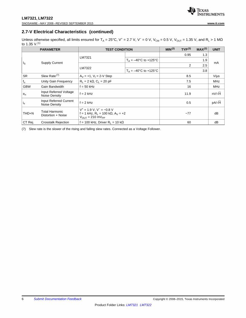
7.6 ±5-V Electrical CharacteristicsUnless otherwise specified, all limited ensured for TA = 25°C, V+ = 5 V, V− = −5V, VCM = 0 V, VOUT = 0 V, and RL > 1 MΩ to 0V. (1)
PARAMETER TEST CONDITION MIN (2) TYP (3) MAX (2) UNIT−5 ±0.7 +5VCM = −4.5 V and VCM =VOS Input Offset Voltage mV4.5 V TA = –40°C to +125°C −6 +6
Input Offset VoltageTC VOS VCM = −4.5 V and VCM = 4.5 V (4) ±2 µV/°CTemperature DriftVCM = −4.5 V (5) −2.0 −1.2
TA = –40°C to +125°C −2.5IB Input Bias Current µA
VCM = 4.5 V (5) 0.45 1TA = –40°C to +125°C 1.5
20 200VCM = −4.5 V and VCM =IOS Input Offset Current nA4.5 V TA = –40°C to +125°C 30080 100
−5 V ≤ VCM ≤ 3 VTA = –40°C to +125°C 70Common ModeCMRR dBRejection Ratio 65 80
−5 V ≤ VCM ≤ 5 VTA = –40°C to +125°C 62
78 104Power Supply Rejection 2.7 V ≤ VS ≤ 30 V,PSRR dBRatio VCM = −4.5 V TA = –40°C to +125°C 74−5.3 −5.1Common-Mode Voltage CMRR > 50 dBRange (Min) TA = –40°C to +125°C −5
CMVR V5.1 5.3Common-Mode Voltage CMRR > 50 dBRange (Max) TA = –40°C to +125°C 574 80−4 V ≤ VO ≤ 4 V
RL = 10 kΩ to 0 V TA = –40°C to +125°C 70Open-Loop VoltageAVOL dBGain 68 74−4 V ≤ VO ≤ 4 VRL = 2 kΩ to 0 V TA = –40°C to +125°C 65
100 250RL = 10 kΩ to 0 VVID = 100 mV TA = –40°C to +125°C 280Output Voltage Swing
High 160 350RL = 2 kΩ to 0 V mVVID = 100 mV TA = –40°C to +125°C 450 fromVOUT either35 200RL = 10 kΩ to 0 V railVID = −100 mV TA = –40°C to +125°C 250Output Voltage SwingLow 80 200RL = 2 kΩ to 0 V
VID = −100 mV TA = –40°C to +125°C 250Sourcing 35 70VID = 200 mV, VOUT = −5
TA = –40°C to +125°C 20V (6)IOUT Output Current mA
Sinking 50 85VID = −200 mV, VOUT = 5
TA = –40°C to +125°C 30V (6)
(1) Electrical Table values apply only for factory testing conditions at the temperature indicated. Factory testing conditions result in verylimited self-heating of the device such that TJ = TA. No ensured specification of parametric performance is indicated in the electricaltables under conditions of internal self-heating where TJ > TA.
(2) All limits are ensured by testing or statistical analysis.(3) Typical values represent the most likely parametric norm as determined at the time of characterization. Actual typical values may vary
over time and will also depend on the application and configuration. The typical values are not tested and are not ensured on shippedproduction material.
(4) Offset voltage temperature drift determined by dividing the change in VOS at temperature extremes into the total temperature change.(5) Positive current corresponds to current flowing into the device.(6) Applies to both single-supply and split-supply operation. Continuous short circuit operation at elevated ambient temperature can result in
exceeding the maximum allowed junction temperature of 150°C. Short circuit test is a momentary test. Output short circuit duration isinfinite for VS ≤ 6 V at room temperature and below. For VS > 6 V, allowable short circuit duration is 1.5 ms.
Copyright © 2008–2015, Texas Instruments Incorporated Submit Documentation Feedback 7
Product Folder Links: LM7321 LM7322

LM7321, LM7322SNOSAW8E –MAY 2008–REVISED SEPTEMBER 2015 www.ti.com
±5-V Electrical Characteristics (continued)Unless otherwise specified, all limited ensured for TA = 25°C, V+ = 5 V, V− = −5V, VCM = 0 V, VOUT = 0 V, and RL > 1 MΩ to 0V.(1)
PARAMETER TEST CONDITION MIN (2) TYP (3) MAX (2) UNIT1.0 1.3
LM7321 TA = –40°C to 2+125°CIS Supply Current VCM = −4.5 V mA
2.3 2.8LM7322 TA = –40°C to 3.8+125°C
SR Slew Rate (7) AV = +1, VI = 8-V Step 12.3 V/µsfu Unity Gain Frequency RL = 2 kΩ, CL = 20 pF 9 MHzGBW Gain Bandwidth f = 50 kHz 16 MHz
Input Referred Voltage f = 2 kHzen 14.3 nV/√HNoise DensityInput Referred Current f = 2 kHzin 1.35 pA/√HNoise DensityTotal Harmonic f = 1 kHz, RL = 100 kΩ, AV = +2THD+N −79 dBDistortion + Noise VOUT = 8 VPP
CT Rej. Crosstalk Rejection f = 100 kHz, Driver RL = 10 kΩ 60 dB
(7) Slew rate is the slower of the rising and falling slew rates. Connected as a Voltage Follower.
7.7 ±15-V Electrical CharacteristicsUnless otherwise specified, all limited ensured for TA = 25°C, V+ = 15 V, V− = −15 V, VCM = 0 V, VOUT = 0 V, and RL > 1 MΩ to15 V. (1)
PARAMETER TEST CONDITION MIN (2) TYP (3) MAX (2) UNIT−6 ±0.7 +6VCM = −14.5 V andVOS Input Offset Voltage mVVCM = 14.5 V –40°C to +125°C −8 +8
Input Offset VoltageTC VOS VCM = −14.5 V and VCM = 14.5 V (4) ±2 µV/°CTemperature Drift−2 −1.1
VCM = −14.5 V (5)–40°C to +125°C −2.5
IB Input Bias Current µA0.45 1
VCM = 14.5 V (5)–40°C to +125°C 1.5
30 300VCM = −14.5 V andIOS Input Offset Current nAVCM = 14.5 V –40°C to +125°C 50080 100
−15 V ≤ VCM ≤ 12 V–40°C to +125°C 75Common-Mode RejectionCMRR dBRatio 72 80
−15 V ≤ VCM ≤ 15 V–40°C to +125°C 70
78 100Power Supply Rejection 2.7 V ≤ VS ≤ 30 V, VCMPSRR dBRatio = −14.5 V –40°C to +125°C 74
(1) Electrical Table values apply only for factory testing conditions at the temperature indicated. Factory testing conditions result in verylimited self-heating of the device such that TJ = TA. No ensured specification of parametric performance is indicated in the electricaltables under conditions of internal self-heating where TJ > TA.
(2) All limits are ensured by testing or statistical analysis.(3) Typical values represent the most likely parametric norm as determined at the time of characterization. Actual typical values may vary
over time and will also depend on the application and configuration. The typical values are not tested and are not ensured on shippedproduction material.
(4) Offset voltage temperature drift determined by dividing the change in VOS at temperature extremes into the total temperature change.(5) Positive current corresponds to current flowing into the device.
8 Submit Documentation Feedback Copyright © 2008–2015, Texas Instruments Incorporated
Product Folder Links: LM7321 LM7322

LM7321, LM7322www.ti.com SNOSAW8E –MAY 2008–REVISED SEPTEMBER 2015
±15-V Electrical Characteristics (continued)Unless otherwise specified, all limited ensured for TA = 25°C, V+ = 15 V, V− = −15 V, VCM = 0 V, VOUT = 0 V, and RL > 1 MΩ to15 V.(1)
PARAMETER TEST CONDITION MIN (2) TYP (3) MAX (2) UNIT−15.3 −15.1Common-Mode Voltage CMRR > 50 dBRange (Min) –40°C to +125°C −15
CMVR V15.1 15.3Common-Mode Voltage CMRR > 50 dBRange (Max) –40°C to +125°C 15
75 85−13 V ≤ VO ≤ 13 VRL = 10 kΩ to 0 V –40°C to +125°C 70
AVOL Open-Loop Voltage Gain dB70 78−13 V ≤ VO ≤ 13 V
RL = 2 kΩ to 0 V –40°C to +125°C 65150 300RL = 10 kΩ to 0 V
VID = 100 mV –40°C to +125°C 350Output Voltage SwingHigh 250 550RL = 2 kΩ to 0 V mVVID = 100 mV –40°C to +125°C 650 fromVOUT either60 200RL = 10 kΩ to 0 V railVID = −100 mV –40°C to +125°C 250Output Voltage SwingLow 130 300RL = 2 kΩ to 0 V
VID = −100 mV –40°C to +125°C 400Sourcing 40 65VID = 200 mV, VOUT = −15 V (6)
IOUT Output Current mASinking 60 100VID = −200 mV, VOUT = 15 V (6)
1.1 1.7LM7321
–40°C to +125°C 2.4IS Supply Current VCM = −14.5 V mA
2.5 4LM7322
–40°C to +125°C 5.6SR Slew Rate (7) AV = +1, VI = 20-V Step 18 V/µsfu Unity Gain Frequency RL = 2 kΩ, CL = 20 pF 11.3 MHzGBW Gain Bandwidth f = 50 kHz 20 MHz
Input Referred Voltage f = 2 kHzen 15 nV/√HNoise DensityInput Referred Currentin f = 2 kHz 1.3 pA/√HNoise DensityTotal Harmonic Distortion f = 1 kHz, RL 100 kΩ,THD+N −86 dB+Noise AV = +2, VOUT = 23 VPP
CT Rej. Crosstalk Rejection f = 100 kHz, Driver RL = 10 kΩ 60 dB
(6) Applies to both single-supply and split-supply operation. Continuous short circuit operation at elevated ambient temperature can result inexceeding the maximum allowed junction temperature of 150°C. Short circuit test is a momentary test. Output short circuit duration isinfinite for VS ≤ 6 V at room temperature and below. For VS > 6 V, allowable short circuit duration is 1.5 ms.
(7) Slew rate is the slower of the rising and falling slew rates. Connected as a Voltage Follower.
Copyright © 2008–2015, Texas Instruments Incorporated Submit Documentation Feedback 9
Product Folder Links: LM7321 LM7322

0.1 1 10 100
ISOURCE (mA)
0.01
0.1
1
10
VO
UT fr
om V
+ (
V)
VS = ±15V
125°C
85°C
25°C-40°C
0.1 1 10 100
ISINK (mA)
0.01
0.1
1
10
VO
UT fr
om V
- (V
)
VS = ±15V
125°C
85°C
25°C
-40°C
0.1 1 10 100
ISOURCE (mA)
0.01
0.1
1
10
VO
UT fr
om V
+ (
V)
VS = ±5V
125°C
85°C
25°C-40°C
0.1 1 10 100
ISINK (mA)
0.01
0.1
1
10
VO
UT fr
om V
- (V
)
VS = ±5V
125°C
85°C
25°C
-40°C
0.1 1 10 100
ISOURCE (mA)
0.01
0.1
1
10
VO
UT fr
om V
+ (
V)
VS = 2.7V
125°C
85°C
25°C-40°C
0.1 1 10 100
ISINK (mA)
0.01
0.1
1
10
VO
UT fr
om V
- (V
)
VS = 2.7V
125°C
85°C
25°C
-40°C
LM7321, LM7322SNOSAW8E –MAY 2008–REVISED SEPTEMBER 2015 www.ti.com
7.8 Typical CharacteristicsUnless otherwise specified: TA = 25°C.
Figure 1. Output Swing vs. Sourcing Current Figure 2. Output Swing vs. Sinking Current
Figure 3. Output Swing vs. Sourcing Current Figure 4. Output Swing vs. Sinking Current
Figure 5. Output Swing vs. Sourcing Current Figure 6. Output Swing vs. Sinking Current
10 Submit Documentation Feedback Copyright © 2008–2015, Texas Instruments Incorporated
Product Folder Links: LM7321 LM7322

-6 -4 -2 0 0 4 6
VCM (V)
-0.8
-0.7
-0.6
-0.5
-0.4
-0.3
VO
S (
mV
)
25°C
VS = ±5V
85°C
125°C
-40°C
-6 -4 -2 0 2 4 6
VCM (V)
-2.5
-2.25
-2
-1.75
-1.5
-1.25
-1
VO
S (
mV
)
VS = ±5V
-40°C
25°C
85°C
125°C
-1 0 1 2 3 4-2.5
-2.3
-2.1
-1.9
-1.7
-1.5
-1.3
-1.1
-0.9
-0.7
-0.5
VO
S (
mV
)
VCM (V)
-40°C
25°C
85°C
125°C
VS = 2.7V
-1 0 1 2 3 4-0.8
-0.7
-0.6
-0.5
-0.4
-0.3
-0.2
-0.1
0
VO
S (
mV
)
VCM (V)
85°C
-40°C
-40°C
125°C
25°C
125°C
VS = 2.7V
-3 -2 -1 0 1 2 3
VOS (mV)
0
2
4
6
8
10
12
PE
RC
EN
TA
GE
(%
)
VS = ±5V
-1 0 1 2 3 4-2.5
-2.3
-2.1
-1.9
-1.7
-1.5
-1.3
-1.1
-0.9
-0.7
-0.5
VO
S (
mV
)
VCM (V)
-40°C
25°C
85°C
125°C
VS = 2.7V
LM7321, LM7322www.ti.com SNOSAW8E –MAY 2008–REVISED SEPTEMBER 2015
Typical Characteristics (continued)Unless otherwise specified: TA = 25°C.
Figure 7. VOS Distribution Figure 8. VOS vs. VCM (Unit 1)
Figure 9. VOS vs. VCM (Unit 2) Figure 10. VOS vs. VCM (Unit 3)
Figure 11. VOS vs. VCM (Unit 1) Figure 12. VOS vs. VCM (Unit 2)
Copyright © 2008–2015, Texas Instruments Incorporated Submit Documentation Feedback 11
Product Folder Links: LM7321 LM7322

0 10 20 30 40-2.5
-2.3
-2.1
-1.9
-1.7
-1.5
-1.3
-1.1
VO
S (
mV
)
VS (V)
-40°C
25°C
85°C
125°C
VCM = V- +0.5V
0 5 10 15 20 25 30 35 40
VS (V)
-0.7
-0.6
-0.5
-0.4
-0.3
-0.2
-0.1
0
VO
S (
mV
)
VCM = V- +0.5V
85°C
125°C
-40°C
25°C
-20 -15 -10 -5 0 5 10 15 20-1
0
VO
S (
mV
)
VCM (V)
-0.9
-0.8
-0.7
-0.6
-0.5
-0.4
-0.3
-0.2
-0.1VS = ±15V
-40°C
25°C
85°C125°C
-20 -15 -10 -5 0 5 10 15 20-2.5
-0.5
VO
S (
mV
)
VCM (V)
-2.3
-2.1
-1.9
-1.7
-1.5
-1.3
-1.1
-0.9
-0.7VS = ±15V
-40°C
25°C
85°C
125°C
-6 -4 -2 0 2 4 6
VCM (V)
-2.5
-2.25
-2
-1.75
-1.5
-1.25
-1
-0.75
-0.5
VO
S (
mV
)
-40°C
25°C
85°C
125°C
VS = ±5V
-20 -15 -10 -5 0 5 10 15 20
VCM (V)
VO
S (
mV
)
-2.25
-2
-1.75
-1.5
-1.25
-1VS = ±15V
-40°C
25°C
85°C
125°C
LM7321, LM7322SNOSAW8E –MAY 2008–REVISED SEPTEMBER 2015 www.ti.com
Typical Characteristics (continued)Unless otherwise specified: TA = 25°C.
Figure 14. VOS vs. VCM (Unit 1)Figure 13. VOS vs. VCM (Unit 2)
Figure 15. VOS vs. VCM (Unit 2) Figure 16. VOS vs. VCM (Unit 3)
Figure 18. VOS vs. VS (Unit 2)Figure 17. VOS vs. VS (Unit 1)
12 Submit Documentation Feedback Copyright © 2008–2015, Texas Instruments Incorporated
Product Folder Links: LM7321 LM7322
-5 -3 -1 1 3 5-1.5
-1
-0.5
0
0.5
1
I BA
IS (P
A)
VCM (V)
VS = ±5V
-40°C
25°C125°C 85°C
0 0.5 1 1.5 2 2.5 3
VCM (V)
-1.5
-1
-0.5
0
0.5
1
I BIA
S (P
A)
VS = 2.7V -40°C25°C
85°C 125°C
0 5 10 15 20 25 30 35 40
VS (V)
-2.2
-2
-1.8
-1.6
-1.4
-1.2
-1
VO
S (
mV
)-40°C
25°C
85°C
125°C
VCM = V+ -0.5V
0 5 10 15 20 25 30 35 40-1
0
VO
S (
mV
)
VS (V)
-0.9
-0.8
-0.7
-0.6
-0.5
-0.4
-0.3
-0.2
-0.1
85°C
125°C
25°C
-40°C
VCM = V+ -0.5V
0 5 10 15 20 25 30 35 40
VS (V)
-2.5
-2
-1.5
-1
-0.5
0
VO
S (
mV
)
-40°C
25°C
85°C
125°C
VCM = V- +0.5V
0 5 10 15 20 25 30 35 40
VS (V)
-2
-1.8
-1.6
-1.4
-1.2
-1
VO
S (
mV
)
VCM = V+ -0.5V
-40°C
25°C
85°C
125°C
LM7321, LM7322www.ti.com SNOSAW8E –MAY 2008–REVISED SEPTEMBER 2015
Typical Characteristics (continued)Unless otherwise specified: TA = 25°C.
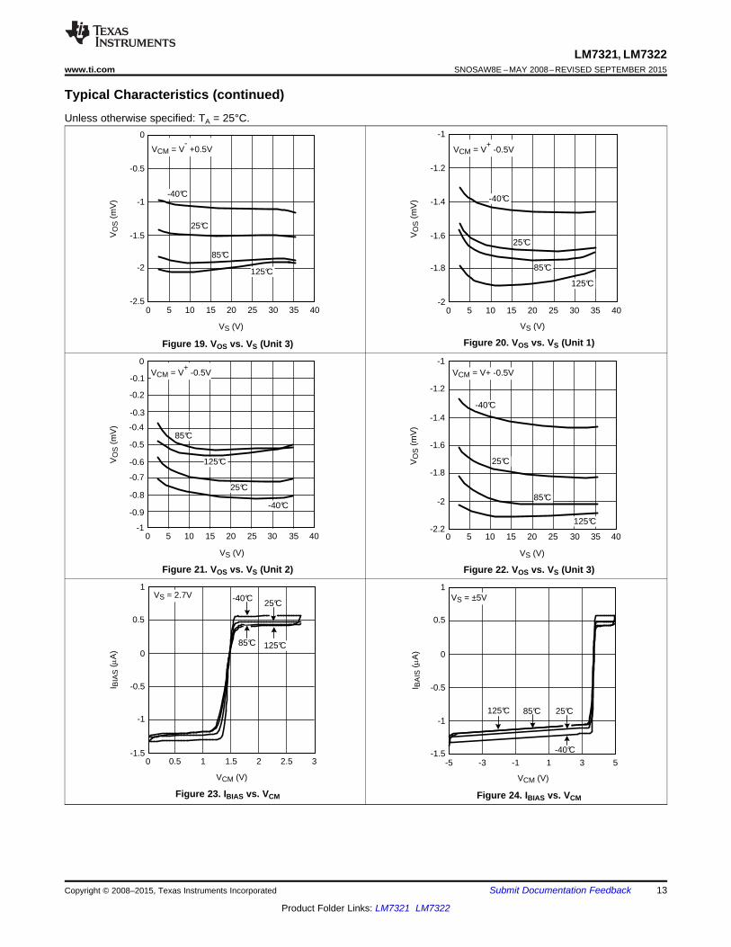
Figure 20. VOS vs. VS (Unit 1)Figure 19. VOS vs. VS (Unit 3)
Figure 21. VOS vs. VS (Unit 2) Figure 22. VOS vs. VS (Unit 3)
Figure 23. IBIAS vs. VCM Figure 24. IBIAS vs. VCM
Copyright © 2008–2015, Texas Instruments Incorporated Submit Documentation Feedback 13
Product Folder Links: LM7321 LM7322

-6 -4 -2 0 2 4 60
0.2
0.4
0.6
0.8
1
1.2
1.4
1.6
1.8
2
I S (
mA
)
VCM (V)
VS = ±5V
125°C
85°C
25°C
-40°C
-1 0 1 2 3 40
0.5
1
1.5
2
2.5
3
3.5
I S (
mA
)
VCM (V)
125°C
85°C
25°C
-40°C
VS = 2.7V
-1 0 1 2 3 40
0.2
0.4
0.6
0.8
1
1.2
1.4
1.6
1.8
I S (
mA
)
VCM (V)
VS = 2.7V 125°C
85°C
25°C
-40°C
0 10 20 30 400.3
0.35
0.4
0.45
0.5
0.55
0.6
0.65
0.7
I BIA
S (P
A)
VS (V)
VCM = V+ -0.5V
-40°C
25°C
85°C
125°C
-15 -10 -5 0 5 10 15
VCM (V)
-1.5
-1
-0.5
0
0.5
1
I BIA
S (P
A)
VS = ±15V
125°C85°C
25°C -40°C
0 5 10 15 20 25 30 35 40
VS (V)
-1.6
-1.5
-1.4
-1.3
-1.2
-1.1
-1
I BIA
S (P
A)
VCM = V- +0.5V
-40°C
25°C
85°C 125°C
LM7321, LM7322SNOSAW8E –MAY 2008–REVISED SEPTEMBER 2015 www.ti.com
Typical Characteristics (continued)Unless otherwise specified: TA = 25°C.
Figure 26. IBIAS vs. VSFigure 25. IBIAS vs. VCM
Figure 27. IBIAS vs. VS Figure 28. IS vs. VCM (LM7321)
Figure 29. IS vs. VCM (LM7322) Figure 30. IS vs. VCM (LM7321)
14 Submit Documentation Feedback Copyright © 2008–2015, Texas Instruments Incorporated
Product Folder Links: LM7321 LM7322

0 5 10 15 20 25 30 35 400
4.5
I S (
mA
)
VS (V)
0.5
1
1.5
2
2.5
3
3.5
4
125°C85°C
25°C
-40°C
VCM = V+
-0.5V
0 10 20 30 400
0.5
1
1.5
2
2.5
I S (
mA
)
VS (V)
VCM = V+ -0.5V
125°C85°C
25°C
-40°C
5 15 25 35
0 10 20 30 400
0.2
0.4
0.6
0.8
1
1.2
1.4
1.6
I S (
mA
)
VS (V)
125°C
85°C
25°C
-40°C
VCM = V- +0.5V
5 15 25 30-20 -15 -10 -5 0 5 10 15 200
4.5
I S (
mA
)
VCM (V)
0.5
1
1.5
2
2.5
3
3.5
4
25°C
85°C
25°C
-40°C
VS = ±15V
85°C
-6 -4 -2 0 2 4 6
VCM (V)
0
0.5
1
1.5
2
2.5
3
3.5
4
I S (
mA
)
125°C
25°C
-40°C
VS = ±5V
-20 -15 -10 -5 0 5 10 15 20
VCM (V)
0
0.5
1
1.5
2
2.5
I S (
mA
)
VS = ±15V
125°C
85°C
25°C
-40°C
LM7321, LM7322www.ti.com SNOSAW8E –MAY 2008–REVISED SEPTEMBER 2015
Typical Characteristics (continued)Unless otherwise specified: TA = 25°C.
Figure 31. IS vs. VCM (LM7322) Figure 32. IS vs. VCM (LM7321)
Figure 33. IS vs. VCM (LM7322) Figure 34. IS vs. VS (LM7321)
Figure 36. IS vs. VS (LM7321)Figure 35. IS vs. VS (LM7322)
Copyright © 2008–2015, Texas Instruments Incorporated Submit Documentation Feedback 15
Product Folder Links: LM7321 LM7322

-20
0
20
40
60
140
GA
IN (
dB)
1k 10k 100k 1M 10M
FREQUENCY (Hz)
80
100
120
100M
VS = r15VRL = 10 M:
PHASE
GAIN
0
23
45
68
90
113
135
PH
AS
E (q)
-23
158
20 pF
50 pF
200 pF
100 pF
50 pF
200 pF100 pF
1000 pF
500 pF
1000 pF500 pF
0 10 20 30 400
0.01
0.02
0.03
0.04
0.05
0.06
0.07
VO
UT fr
om R
AIL
(V
)
VS (V)
RL = 10 k:
-40°C
25°C
85°C
125°C
0 10 20 30 400
0.02
0.04
0.06
0.08
0.1
0.12
0.14
0.16
VO
UT fr
om R
AIL
(V
)
VS (V)
RL = 2 k: 125°C
85°C
25°C
-40°C
0 5 10 15 20 25 30 35 40
VS (V)
0
0.02
0.04
0.06
0.08
0.1
0.12
0.14
0.16
VO
UT fr
om R
AIL
(V
)
RL = 10 k:
-40°C
125°C
85°C
25°C
0 10 20 30 400
0.05
0.1
0.15
0.2
0.25
0.3
VO
UT fr
om R
AIL
(V
)
VS (V)
-40°C
125°C
85°C
25°C
RL = 2 k:
0 5 10 15 20 25 30 35 40
VS (V)
0
0.5
1
1.5
2
2.5
3
I S (
mA
)
125°C
85°C
25°C
-40°C
VCM = V- +0.5V
LM7321, LM7322SNOSAW8E –MAY 2008–REVISED SEPTEMBER 2015 www.ti.com
Typical Characteristics (continued)Unless otherwise specified: TA = 25°C.
Figure 37. IS vs. VS (LM7322) Figure 38. Positive Output Swing vs. Supply Voltage
Figure 39. Positive Output Swing vs. Supply Voltage Figure 40. Negative Output Swing vs. Supply Voltage
Figure 42. Open-Loop Frequency Response with VariousFigure 41. Negative Output Swing vs. Supply VoltageCapacitive Load
16 Submit Documentation Feedback Copyright © 2008–2015, Texas Instruments Incorporated
Product Folder Links: LM7321 LM7322

10 1k 1M
FREQUENCY (Hz)
0
40
100
-PS
RR
(dB
)
100k10k100
80
60
20
10
30
50
70
90VS = 30V
VCM = 2V
VS = 10V
VCM = 2V VS = 2.7V
VCM = 2V
10 1k 1M
FREQUENCY (Hz)
0
40
120
+P
SR
R (
dB)
100k10k100
100
60
20
80
VS = 2.7V
VCM = 0.7V
VS = 10V
VCM = 8V
VS = 30V
VCM = 28V
10 100 10000
10
20
30
40
50
60
70
PH
AS
E M
AR
GIN
(°)
CAPACITIVE LOAD (pF)
RL = 600:
RL = 2 k:
RL = 10 M:, 10 k:, 100 k:
VS = ±15V
10 1k 1M
FREQUENCY (Hz)
0
40
100
CM
RR
(dB
)
100k10k100
80
60
20
10
30
50
70
90VS = ±15V
-20
0
20
40
60
140
GA
IN (
dB)
1k 10k 100k 1M 10M
FREQUENCY (Hz)
80
100
120
100M
VS = r15VCL = 20 pFPHASE
GAIN
0
23
45
68
90
113
135
PH
AS
E (q)
-23
158
10 M:
2 k:
600:
100 k:
10 k:
2 k:
600:
-20
0
20
40
60
140
GA
IN (
dB)
1k 10k 100k 1M 10M
FREQUENCY (Hz)
80
100
120
100M
RL = 2 k:CL = 20 pF
0
23
45
68
90
113
135
PH
AS
E (q)
-23
158
VS = 10V
VS = 30V
VS = 2.7V
VS = 30VVS = 2.7V
VS = 10V
PHASE
GAIN
LM7321, LM7322www.ti.com SNOSAW8E –MAY 2008–REVISED SEPTEMBER 2015
Typical Characteristics (continued)Unless otherwise specified: TA = 25°C.
Figure 43. Open-Loop Frequency Response with Various Figure 44. Open-Loop Frequency Response with VariousResistive Load Supply Voltage
Figure 46. CMRR vs. FrequencyFigure 45. Phase Margin vs. Capacitive Load
Figure 47. +PSRR vs. Frequency Figure 48. −PSRR vs. Frequency
Copyright © 2008–2015, Texas Instruments Incorporated Submit Documentation Feedback 17
Product Folder Links: LM7321 LM7322

1 10 100 1k 100k
FREQUENCY (Hz)
1
10
100
1000
10k
CU
RR
EN
T N
OIS
E (
pA/
Hz)
VO
LTA
GE
NO
ISE
(nV
Hz)
0.1
1
10
100
VOLTAGE
CURRENT
VS = ±15V0
10 1k 1M
FREQUENCY (Hz)
-80
-50TH
D+
N (
dB)
100k10k100
-20
-30
-60
-70
-40
-10
VS = 2.7V, VCM = 0.8V
VS = ±5V
VS = ±15V
AV = +2
VIN = 520 mVPP
RL = 100 k:
1 10 100 1k 100k
FREQUENCY (Hz)
1
10
100
1000
10k
CU
RR
EN
T N
OIS
E (
pA/
Hz)
VO
LTA
GE
NO
ISE
(nV
Hz)
0.1
1
10
100
VOLTAGE
CURRENT
VS = 2.7V
1 10 100 1k 100k
FREQUENCY (Hz)
1
10
100
1000
10k
CU
RR
EN
T N
OIS
E (
pA/
Hz)
VO
LTA
GE
NO
ISE
(nV
Hz)
0.1
1
10
100
VOLTAGE
CURRENT
VS = ±5V
25V
/DIV
5 Ps/DIV
VS = ±15V, AV = +1
INPUT
10 pF
2,200 pF
8,600 pF
12,200 pF
1000 pF
750 pF
500 pF
330 pF
100 pF
10 pF
INPUT
100
mV
/DIV
200 ns/DIV
VS = ±5V
AV = +1
LM7321, LM7322SNOSAW8E –MAY 2008–REVISED SEPTEMBER 2015 www.ti.com
Typical Characteristics (continued)Unless otherwise specified: TA = 25°C.
Figure 49. Small Signal Step Response Figure 50. Large Signal Step Response
Figure 51. Input Referred Noise Density vs. Frequency Figure 52. Input Referred Noise Density vs. Frequency
Figure 53. Input Referred Noise Density vs. Frequency Figure 54. THD+N vs. Frequency
18 Submit Documentation Feedback Copyright © 2008–2015, Texas Instruments Incorporated
Product Folder Links: LM7321 LM7322

0.001 0.1 100
OUTPUT AMPLITUDE (VPP)
-90
-70
0
TH
D+
N (
dB)
1010.01
-20
-30
-80
-10
-40
-50
-60
VS = ±15Vf = 1 kHz
RL = 100 k:
AV = +2
0.001 0.01 0.1 1 10
OUTPUT AMPLITUDE (VPP)
-90
-80
-70
-60
-50
-40
-30
-20
-10
0
TH
D+
N (
dB)
VS = 2.7V
VCM = 0.8Vf = 1 kHz
RL = 100 k:
AV = +2
0.001 0.1 100
OUTPUT AMPLITUDE (VPP)
-90
-70
0
TH
D+
N (
dB)
1010.01
-20
-30
-80
-10
-40
-50
-60
VS = ±5Vf = 1 kHz
RL = 100 k:
AV = +2
LM7321, LM7322www.ti.com SNOSAW8E –MAY 2008–REVISED SEPTEMBER 2015
Typical Characteristics (continued)Unless otherwise specified: TA = 25°C.
Figure 56. THD+N vs. Output AmplitudeFigure 55. THD+N vs. Output Amplitude
Figure 57. THD+N vs. Output Amplitude
Copyright © 2008–2015, Texas Instruments Incorporated Submit Documentation Feedback 19
Product Folder Links: LM7321 LM7322

±
+
-IN
+IN
OUT
V+
V-
LM7321, LM7322SNOSAW8E –MAY 2008–REVISED SEPTEMBER 2015 www.ti.com
8 Detailed Description
8.1 OverviewThe LM732xx devices are rail-to-rail input and output amplifiers with wide operating voltages and high-outputcurrents. The LM732xx family is efficient, achieving 18-V/µs slew rate and 20-MHz unity gain bandwidth whilerequiring only 1 mA of supply current per op amp. The LM732xx device performance is fully specified foroperation at 2.7 V, ±5 V and ±15 V.
The LM732xx devices are designed to drive unlimited capacitive loads without oscillations. All LM7321x andLM7322x parts are tested at −40°C, 125°C, and 25°C, with modern automatic test equipment. High performancefrom −40°C to 125°C, detailed specifications, and extensive testing makes them suitable for industrial,automotive, and communications applications.
Greater than rail-to-rail input common-mode voltage range with 50 dB of common-mode rejection across thiswide voltage range, allows both high-side and low-side sensing. Most device parameters are insensitive to powersupply voltage, and this makes the parts easier to use where supply voltage may vary, such as automotiveelectrical systems and battery-powered equipment. These amplifiers have true rail-to-rail output and can supply arespectable amount of current (15 mA) with minimal head room from either rail (300 mV) at low distortion (0.05%THD+Noise).
8.2 Functional Block Diagram
8.3 Feature Description
8.3.1 Output Short Circuit Current and Dissipation IssuesThe LM732xx output stage is designed for maximum output current capability. Even though momentary outputshorts to ground and either supply can be tolerated at all operating voltages, longer lasting short conditions cancause the junction temperature to rise beyond the absolute maximum rating of the device, especially at highersupply voltage conditions. Below supply voltage of 6 V, the output short circuit condition can be toleratedindefinitely.
With the op amp tied to a load, the device power dissipation consists of the quiescent power due to the supplycurrent flow into the device, in addition to power dissipation due to the load current. The load portion of thepower itself could include an average value (due to a DC load current) and an AC component. DC load currentwould flow if there is an output voltage offset, or the output AC average current is non-zero, or if the op ampoperates in a single supply application where the output is maintained somewhere in the range of linearoperation.
Therefore,PTOTAL = PQ + PDC + PAC (1)
20 Submit Documentation Feedback Copyright © 2008–2015, Texas Instruments Incorporated
Product Folder Links: LM7321 LM7322

PD(MAX) = 150°C ± 125°C
165°C/W= 0.15 W
PD(MAX) = 150°C ± 125°C
235°C/W= 0.11 W
PD(MAX) = 150°C ± 25°C
165°C/W= 0.76 W
PD(MAX) = 150°C ± 25°C
235°C/W= 0.53 W
PD(MAX) =
TJ(MAX) - TA
TJA
LM7321, LM7322www.ti.com SNOSAW8E –MAY 2008–REVISED SEPTEMBER 2015
Feature Description (continued)The Op Amp Quiescent Power Dissipation is calculated as:
PQ = IS × VS
where• IS: Supply Current• VS: Total Supply Voltage (V+ − V−) (2)
The DC Load Power is calculated as:PDC = IO × (Vr - Vo)
where• VO: Average Output Voltage• Vr: V+ for sourcing and V− for sinking current (3)
The AC Load Power is calculated as PAC = See Table 1.
Table 1 shows the maximum AC component of the load power dissipated by the op amp for standard Sinusoidal,Triangular, and Square Waveforms:
Table 1. Normalized AC Power Dissipated in the Output Stage for Standard WaveformsPAC (W.Ω/V2)
Sinusoidal Triangular Square50.7 × 10−3 46.9 × 10⁻³ 62.5 × 10⁻³
The table entries are normalized to VS2/RL. To figure out the AC load current component of power dissipation,
simply multiply the table entry corresponding to the output waveform by the factor VS2/RL. For example, with ±12-
V supplies, a 600-Ω load, and triangular waveform power dissipation in the output stage is calculated as:PAC = (46.9 × 10−3) × (242/600) = 45.0 mW (4)
The maximum power dissipation allowed at a certain temperature is a function of maximum die junctiontemperature (TJ(MAX)) allowed, ambient temperature TA, and package thermal resistance from junction to ambient,θJA.
(5)
For the LM732xx, the maximum junction temperature allowed is 150°C at which no power dissipation is allowed.The power capability at 25°C is given by the following calculations:
For VSSOP package:
(6)
For SOIC package:
(7)
Similarly, the power capability at 125°C is given by:
For VSSOP package:
(8)
For SOIC package:
(9)
Copyright © 2008–2015, Texas Instruments Incorporated Submit Documentation Feedback 21
Product Folder Links: LM7321 LM7322

-40 -20 0 20 40 60 80 100 120 140 1600
0.2
0.4
0.6
0.8
1
1.2
1.4
PO
WE
R C
AP
AB
ILIT
Y (
W)
TEMPERATURE (°C)
Operating area
Maximum thermal capability line (SOIC)
Maximum thermal capability line (MSOP)
LM7321, LM7322SNOSAW8E –MAY 2008–REVISED SEPTEMBER 2015 www.ti.com
Figure 58 shows the power capability vs. temperature for VSSOP and SOIC packages. The area under themaximum thermal capability line is the operating area for the device. When the device works in the operatingarea where PTOTAL is less than PD(MAX), the device junction temperature will remain below 150°C. If theintersection of ambient temperature and package power is above the maximum thermal capability line, thejunction temperature will exceed 150°C and this should be strictly prohibited.
Figure 58. Power Capability vs. Temperature
When high power is required and ambient temperature can't be reduced, providing air flow is an effectiveapproach to reduce thermal resistance therefore to improve power capability.
8.3.2 Estimating the Output Voltage SwingIt is important to keep in mind that the steady-state output current will be less than the current available whenthere is an input overdrive present. For steady-state conditions, the Output Voltage vs. Output Current plot(Typical Characteristics section) can be used to predict the output swing. Figure 59 and Figure 60 show thisperformance along with several load lines corresponding to loads tied between the output and ground. In eachcases, the intersection of the device plot at the appropriate temperature with the load line would be the typicaloutput swing possible for that load. For example, a 1-kΩ load can accommodate an output swing to within 250mV of V− and to 330 mV of V+ (VS = ±15 V) corresponding to a typical 29.3 VPP unclipped swing.
Figure 59. Output Sourcing Characteristics With Load Figure 60. Output Sinking Characteristics With Load LinesLines
22 Submit Documentation Feedback Copyright © 2008–2015, Texas Instruments Incorporated
Product Folder Links: LM7321 LM7322

LM7321, LM7322www.ti.com SNOSAW8E –MAY 2008–REVISED SEPTEMBER 2015
8.4 Device Functional Modes
8.4.1 Driving Capacitive LoadsThe LM732xx are specifically designed to drive unlimited capacitive loads without oscillations as shown inFigure 61.
Figure 61. ±5% Settling Time vs. Capacitive Load
In addition, the output current handling capability of the device allows for good slewing characteristics even withlarge capacitive loads as shown in Figure 62 and Figure 63.
Figure 62. +SR vs. Capacitive Load Figure 63. −SR vs. Capacitive Load
The combination of these features is ideal for applications such as TFT flat panel buffers, A/D converter inputamplifiers, and so forth.
However, as in most op amps, addition of a series isolation resistor between the op amp and the capacitive loadimproves the settling and overshoot performance.
Output current drive is an important parameter when driving capacitive loads. This parameter will determine howfast the output voltage can change. Referring to the Slew Rate vs. Capacitive Load Plots (Typical Characteristicssection), two distinct regions can be identified. Below about 10,000 pF, the output Slew Rate is solely determinedby the compensation capacitor value of the op amp and available current into that capacitor. Beyond 10 nF, theSlew Rate is determined by the available output current of the op amp.
Copyright © 2008–2015, Texas Instruments Incorporated Submit Documentation Feedback 23
Product Folder Links: LM7321 LM7322

LM7321, LM7322SNOSAW8E –MAY 2008–REVISED SEPTEMBER 2015 www.ti.com
Device Functional Modes (continued)
NOTEBecause of the lower output sourcing current compared to the sinking one, the Slew Ratelimit under heavy capacitive loading is determined by the positive transitions.
An estimate of positive and negative slew rates for loads larger than 100 nF can be made by dividing the shortcircuit current value by the capacitor.
For the LM732xx, the available output current increases with the input overdrive. Referring to Figure 64 andFigure 65, it can be seen that both sourcing and sinking short circuit current increase as input overdriveincreases. In a closed-loop amplifier configuration, during transient conditions while the fed back output has notquite caught up with the input, there will be an overdrive imposed on the input allowing more output current thanwould normally be available under steady-state condition. Because of this feature, the output stage quiescentcurrent of the op amp can be kept to a minimum, thereby reducing power consumption, while enabling the deviceto deliver large output current when the need arises (such as during transients).
Figure 64. Output Short Circuit Sourcing Current vs. Input Figure 65. Output Short Circuit Sinking Current vs. InputOverdrive Overdrive
Figure 66 shows the output voltage, output current, and the resulting input overdrive with the device set for AV =+1 and the input tied to a 1-VPP step function driving a 47-nF capacitor. As can be seen, during the outputtransition, the input overdrive reaches 1-V peak and is more than enough to cause the output current to increaseto its maximum value (see Figure 64 and Figure 65 plots).
NOTEBecause of the larger output sinking current compared to the sourcing one, the outputnegative transition is faster than the positive one.
Figure 66. Buffer Amplifier Scope Photo
24 Submit Documentation Feedback Copyright © 2008–2015, Texas Instruments Incorporated
Product Folder Links: LM7321 LM7322

LM7321, LM7322www.ti.com SNOSAW8E –MAY 2008–REVISED SEPTEMBER 2015
9 Application and Implementation
NOTEInformation in the following applications sections is not part of the TI componentspecification, and TI does not warrant its accuracy or completeness. TI’s customers areresponsible for determining suitability of components for their purposes. Customers shouldvalidate and test their design implementation to confirm system functionality.
9.1 Application Information
9.1.1 Similar High-Output DevicesThe LM7332 is a dual rail-to-rail amplifier with a slightly lower GBW capable of sinking and sourcing 100 mA. It isavailable in SOIC and VSSOP packages.
The LM4562 is dual op amp with very low noise and 0.7-mV voltage offset.
The LME49870 and LME49860 are single and dual low-noise amplifiers that can work from ±22-V supplies.
9.1.2 Other High Performance SOT-23 AmpliersThe LM7341 is a 4-MHz rail-to-rail input and output part that requires only 0.6 mA to operate, and can driveunlimited capacitive load. It has a voltage gain of 97 dB, a CMRR of 93 dB, and a PSRR of 104 dB.
The LM6211 is a 20-MHz part with CMOS input, which runs on ±12-V or 24-V single supplies. It has rail-to-railoutput and low noise.
The LM7121 has a gain bandwidth of 235 MHz.
Detailed information on these parts can be found at www.ti.com.
9.2 Typical ApplicationFigure 67 shows a typical application where the LM732xx is used as a buffer amplifier for the VCOM signalemployed in a TFT LCD flat panel:
Figure 67. VCOM Driver Application Schematic
9.2.1 Design RequirementsFor this example application, the supply voltage is +5 V, and noninverting gain is necessary.
Copyright © 2008–2015, Texas Instruments Incorporated Submit Documentation Feedback 25
Product Folder Links: LM7321 LM7322

90
1k 100k 10M
FREQUENCY (Hz)
0
30
60
CR
OS
ST
ALK
RE
JEC
TIO
N (
dB)
100M1M10k
80
70
50
40
20
10
VS = ±15V
VS = ±5V
V+ = 1.8V
VCM = 0.9V
LM7321, LM7322SNOSAW8E –MAY 2008–REVISED SEPTEMBER 2015 www.ti.com
Typical Application (continued)9.2.2 Detailed Design ProcedureFigure 68 shows the time domain response of the amplifier when used as a VCOM buffer/driver with VREF atground. In this application, the op amp loop will try and maintain its output voltage based on the voltage on itsnoninverting input (VREF) despite the current injected into the TFT simulated load. As long as this load current iswithin the range tolerable by the LM732xx (45-mA sourcing and 65-mA sinking for ±5-V supplies), the output willsettle to its final value within less than 2 μs.
Figure 68. VCOM Driver Performance Scope Photo
9.2.3 Application Curve
Figure 69. Crosstalk Rejection vs. Frequency
26 Submit Documentation Feedback Copyright © 2008–2015, Texas Instruments Incorporated
Product Folder Links: LM7321 LM7322

LM7321, LM7322www.ti.com SNOSAW8E –MAY 2008–REVISED SEPTEMBER 2015
10 Power Supply RecommendationsThe use of supply decoupling is mandatory in most applications. As with most relatively high-speed or high-output current op amps, best results are achieved when each supply line is decoupled with two capacitors; asmall value ceramic capacitor ( about 0.01 μF) placed very close to the supply lead in addition to a large valueTantalum or Aluminum (> 4.7 μF). The large capacitor can be shared by more than one device if necessary. Thesmall ceramic capacitor maintains low supply impedance at high frequencies while the large capacitor will act asthe charge bucket for fast load current spikes at the op amp output. The combination of these capacitors willprovide supply decoupling and will help keep the op amp oscillation free under any load.
11 Layout
11.1 Layout GuidelinesTake care to minimize the loop area formed by the bypass capacitor connection between supply pins andground. A ground plane underneath the device is recommended; any bypass components to ground should havea nearby via to the ground plane. The optimum bypass capacitor placement is closest to the correspondingsupply pin. Use of thicker traces from the bypass capacitors to the corresponding supply pins will lower thepower supply inductance and provide a more stable power supply.
The feedback components should be placed as close to the device as possible to minimize stray parasitics.
11.2 Layout Example
Figure 70. LM732xx Layout Example
Copyright © 2008–2015, Texas Instruments Incorporated Submit Documentation Feedback 27
Product Folder Links: LM7321 LM7322

LM7321, LM7322SNOSAW8E –MAY 2008–REVISED SEPTEMBER 2015 www.ti.com
12 Device and Documentation Support
12.1 Related LinksThe table below lists quick access links. Categories include technical documents, support and communityresources, tools and software, and quick access to sample or buy.
Table 2. Related LinksTECHNICAL TOOLS & SUPPORT &PARTS PRODUCT FOLDER SAMPLE & BUY DOCUMENTS SOFTWARE COMMUNITY
LM7321 Click here Click here Click here Click here Click hereLM7322 Click here Click here Click here Click here Click here
12.2 Community ResourcesThe following links connect to TI community resources. Linked contents are provided "AS IS" by the respectivecontributors. They do not constitute TI specifications and do not necessarily reflect TI's views; see TI's Terms ofUse.
TI E2E™ Online Community TI's Engineer-to-Engineer (E2E) Community. Created to foster collaborationamong engineers. At e2e.ti.com, you can ask questions, share knowledge, explore ideas and helpsolve problems with fellow engineers.
Design Support TI's Design Support Quickly find helpful E2E forums along with design support tools andcontact information for technical support.
12.3 TrademarksE2E is a trademark of Texas Instruments.All other trademarks are the property of their respective owners.
12.4 Electrostatic Discharge CautionThese devices have limited built-in ESD protection. The leads should be shorted together or the device placed in conductive foamduring storage or handling to prevent electrostatic damage to the MOS gates.
12.5 GlossarySLYZ022 — TI Glossary.
This glossary lists and explains terms, acronyms, and definitions.
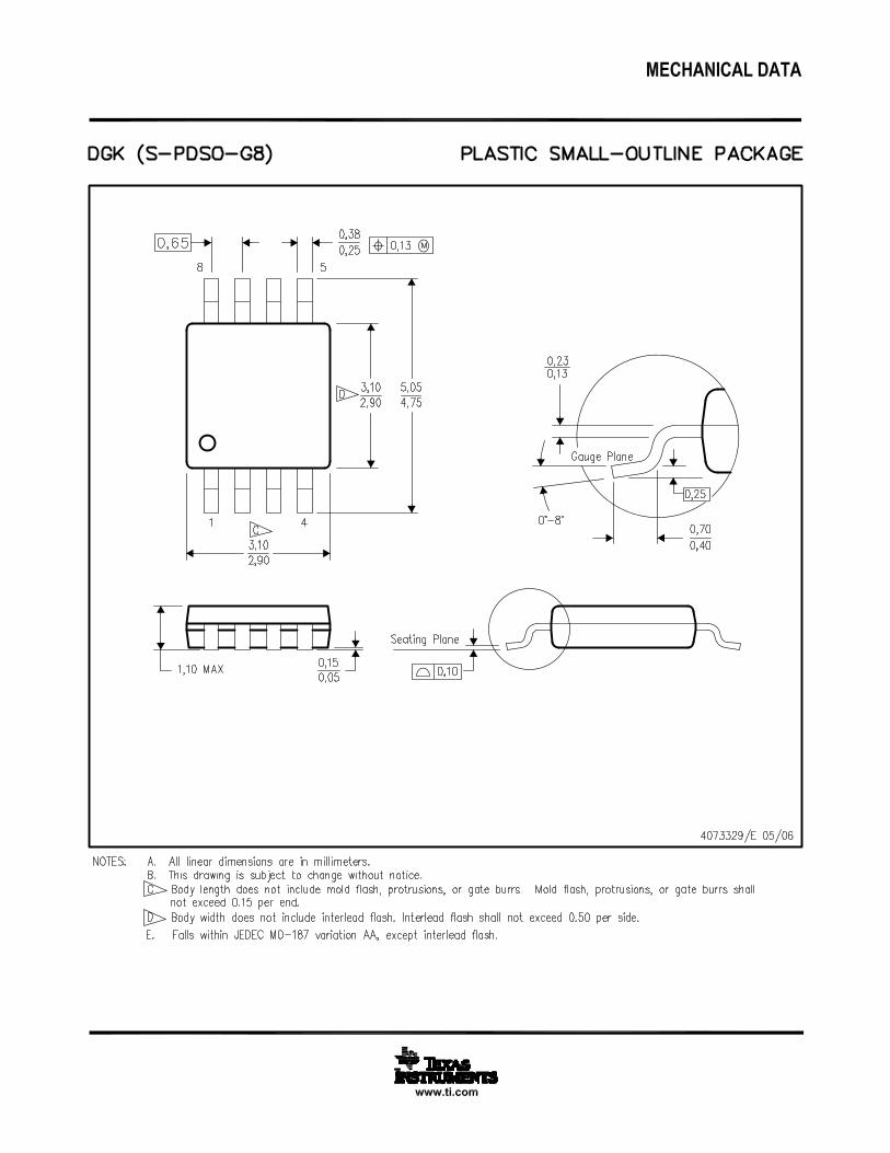
13 Mechanical, Packaging, and Orderable InformationThe following pages include mechanical, packaging, and orderable information. This information is the mostcurrent data available for the designated devices. This data is subject to change without notice and revision ofthis document. For browser-based versions of this data sheet, refer to the left-hand navigation.
28 Submit Documentation Feedback Copyright © 2008–2015, Texas Instruments Incorporated
Product Folder Links: LM7321 LM7322

PACKAGE OPTION ADDENDUM
www.ti.com 8-Oct-2015
Addendum-Page 1
PACKAGING INFORMATION
Orderable Device Status(1)
Package Type PackageDrawing
Pins PackageQty
Eco Plan(2)
Lead/Ball Finish(6)
MSL Peak Temp(3)
Op Temp (°C) Device Marking(4/5)
Samples
LM7321MA/NOPB ACTIVE SOIC D 8 95 Green (RoHS& no Sb/Br)
CU SN Level-1-260C-UNLIM -40 to 125 LM7321MA
LM7321MAX/NOPB ACTIVE SOIC D 8 2500 Green (RoHS& no Sb/Br)
CU SN Level-1-260C-UNLIM -40 to 125 LM7321MA
LM7321MF/NOPB ACTIVE SOT-23 DBV 5 1000 Green (RoHS& no Sb/Br)
CU SN Level-1-260C-UNLIM -40 to 125 AU4A
LM7321MFE/NOPB ACTIVE SOT-23 DBV 5 250 Green (RoHS& no Sb/Br)
CU SN Level-1-260C-UNLIM -40 to 125 AU4A
LM7321MFX/NOPB ACTIVE SOT-23 DBV 5 3000 Green (RoHS& no Sb/Br)
CU SN Level-1-260C-UNLIM -40 to 125 AU4A
LM7321QMF/NOPB ACTIVE SOT-23 DBV 5 1000 Green (RoHS& no Sb/Br)
CU SN Level-1-260C-UNLIM -40 to 125 AR8A
LM7321QMFE/NOPB ACTIVE SOT-23 DBV 5 250 Green (RoHS& no Sb/Br)
CU SN Level-1-260C-UNLIM -40 to 125 AR8A
LM7321QMFX/NOPB ACTIVE SOT-23 DBV 5 3000 Green (RoHS& no Sb/Br)
CU SN Level-1-260C-UNLIM -40 to 125 AR8A
LM7322MA/NOPB ACTIVE SOIC D 8 95 Green (RoHS& no Sb/Br)
CU SN Level-1-260C-UNLIM -40 to 125 LM7322MA
LM7322MAX/NOPB ACTIVE SOIC D 8 2500 Green (RoHS& no Sb/Br)
CU SN Level-1-260C-UNLIM -40 to 125 LM7322MA
LM7322MM/NOPB ACTIVE VSSOP DGK 8 1000 Green (RoHS& no Sb/Br)
CU SN Level-1-260C-UNLIM -40 to 125 AZ4A
LM7322MME/NOPB ACTIVE VSSOP DGK 8 250 Green (RoHS& no Sb/Br)
CU SN Level-1-260C-UNLIM -40 to 125 AZ4A
LM7322QMA/NOPB ACTIVE SOIC D 8 95 Green (RoHS& no Sb/Br)
CU SN Level-1-260C-UNLIM -40 to 125 LM7322QMA
LM7322QMAX/NOPB ACTIVE SOIC D 8 2500 Green (RoHS& no Sb/Br)
CU SN Level-1-260C-UNLIM -40 to 125 LM7322QMA
(1) The marketing status values are defined as follows:ACTIVE: Product device recommended for new designs.LIFEBUY: TI has announced that the device will be discontinued, and a lifetime-buy period is in effect.NRND: Not recommended for new designs. Device is in production to support existing customers, but TI does not recommend using this part in a new design.PREVIEW: Device has been announced but is not in production. Samples may or may not be available.OBSOLETE: TI has discontinued the production of the device.

PACKAGE OPTION ADDENDUM
www.ti.com 8-Oct-2015
Addendum-Page 2
(2) Eco Plan - The planned eco-friendly classification: Pb-Free (RoHS), Pb-Free (RoHS Exempt), or Green (RoHS & no Sb/Br) - please check http://www.ti.com/productcontent for the latest availabilityinformation and additional product content details.TBD: The Pb-Free/Green conversion plan has not been defined.Pb-Free (RoHS): TI's terms "Lead-Free" or "Pb-Free" mean semiconductor products that are compatible with the current RoHS requirements for all 6 substances, including the requirement thatlead not exceed 0.1% by weight in homogeneous materials. Where designed to be soldered at high temperatures, TI Pb-Free products are suitable for use in specified lead-free processes.Pb-Free (RoHS Exempt): This component has a RoHS exemption for either 1) lead-based flip-chip solder bumps used between the die and package, or 2) lead-based die adhesive used betweenthe die and leadframe. The component is otherwise considered Pb-Free (RoHS compatible) as defined above.Green (RoHS & no Sb/Br): TI defines "Green" to mean Pb-Free (RoHS compatible), and free of Bromine (Br) and Antimony (Sb) based flame retardants (Br or Sb do not exceed 0.1% by weightin homogeneous material)
(3) MSL, Peak Temp. - The Moisture Sensitivity Level rating according to the JEDEC industry standard classifications, and peak solder temperature.
(4) There may be additional marking, which relates to the logo, the lot trace code information, or the environmental category on the device.
(5) Multiple Device Markings will be inside parentheses. Only one Device Marking contained in parentheses and separated by a "~" will appear on a device. If a line is indented then it is a continuationof the previous line and the two combined represent the entire Device Marking for that device.
(6) Lead/Ball Finish - Orderable Devices may have multiple material finish options. Finish options are separated by a vertical ruled line. Lead/Ball Finish values may wrap to two lines if the finishvalue exceeds the maximum column width.
Important Information and Disclaimer:The information provided on this page represents TI's knowledge and belief as of the date that it is provided. TI bases its knowledge and belief on informationprovided by third parties, and makes no representation or warranty as to the accuracy of such information. Efforts are underway to better integrate information from third parties. TI has taken andcontinues to take reasonable steps to provide representative and accurate information but may not have conducted destructive testing or chemical analysis on incoming materials and chemicals.TI and TI suppliers consider certain information to be proprietary, and thus CAS numbers and other limited information may not be available for release.
In no event shall TI's liability arising out of such information exceed the total purchase price of the TI part(s) at issue in this document sold by TI to Customer on an annual basis.
OTHER QUALIFIED VERSIONS OF LM7321, LM7321-Q1, LM7322, LM7322-Q1 :
• Catalog: LM7321, LM7322
• Automotive: LM7321-Q1, LM7322-Q1
NOTE: Qualified Version Definitions:
• Catalog - TI's standard catalog product

PACKAGE OPTION ADDENDUM
www.ti.com 8-Oct-2015
Addendum-Page 3
• Automotive - Q100 devices qualified for high-reliability automotive applications targeting zero defects

TAPE AND REEL INFORMATION
*All dimensions are nominal
Device PackageType
PackageDrawing
Pins SPQ ReelDiameter
(mm)
ReelWidth
W1 (mm)
A0(mm)
B0(mm)
K0(mm)
P1(mm)
W(mm)
Pin1Quadrant
LM7321MAX/NOPB SOIC D 8 2500 330.0 12.4 6.5 5.4 2.0 8.0 12.0 Q1
LM7321MF/NOPB SOT-23 DBV 5 1000 178.0 8.4 3.2 3.2 1.4 4.0 8.0 Q3
LM7321MFE/NOPB SOT-23 DBV 5 250 178.0 8.4 3.2 3.2 1.4 4.0 8.0 Q3
LM7321MFX/NOPB SOT-23 DBV 5 3000 178.0 8.4 3.2 3.2 1.4 4.0 8.0 Q3
LM7321QMF/NOPB SOT-23 DBV 5 1000 178.0 8.4 3.2 3.2 1.4 4.0 8.0 Q3
LM7321QMFE/NOPB SOT-23 DBV 5 250 178.0 8.4 3.2 3.2 1.4 4.0 8.0 Q3
LM7321QMFX/NOPB SOT-23 DBV 5 3000 178.0 8.4 3.2 3.2 1.4 4.0 8.0 Q3
LM7322MAX/NOPB SOIC D 8 2500 330.0 12.4 6.5 5.4 2.0 8.0 12.0 Q1
LM7322MM/NOPB VSSOP DGK 8 1000 178.0 12.4 5.3 3.4 1.4 8.0 12.0 Q1
LM7322MME/NOPB VSSOP DGK 8 250 178.0 12.4 5.3 3.4 1.4 8.0 12.0 Q1
LM7322QMAX/NOPB SOIC D 8 2500 330.0 12.4 6.5 5.4 2.0 8.0 12.0 Q1
PACKAGE MATERIALS INFORMATION
www.ti.com 20-Dec-2016
Pack Materials-Page 1
*All dimensions are nominal
Device Package Type Package Drawing Pins SPQ Length (mm) Width (mm) Height (mm)
LM7321MAX/NOPB SOIC D 8 2500 367.0 367.0 35.0
LM7321MF/NOPB SOT-23 DBV 5 1000 210.0 185.0 35.0
LM7321MFE/NOPB SOT-23 DBV 5 250 210.0 185.0 35.0
LM7321MFX/NOPB SOT-23 DBV 5 3000 210.0 185.0 35.0
LM7321QMF/NOPB SOT-23 DBV 5 1000 210.0 185.0 35.0
LM7321QMFE/NOPB SOT-23 DBV 5 250 210.0 185.0 35.0
LM7321QMFX/NOPB SOT-23 DBV 5 3000 210.0 185.0 35.0
LM7322MAX/NOPB SOIC D 8 2500 367.0 367.0 35.0
LM7322MM/NOPB VSSOP DGK 8 1000 210.0 185.0 35.0
LM7322MME/NOPB VSSOP DGK 8 250 210.0 185.0 35.0
LM7322QMAX/NOPB SOIC D 8 2500 367.0 367.0 35.0
PACKAGE MATERIALS INFORMATION
www.ti.com 20-Dec-2016
Pack Materials-Page 2

www.ti.com
PACKAGE OUTLINE
C
TYP0.220.08
0.25
3.02.6
2X 0.95
1.9
1.45 MAX
TYP0.150.00
5X 0.50.3
TYP0.60.3
TYP80
1.9
A
3.052.75
B1.751.45
(1.1)
SOT-23 - 1.45 mm max heightDBV0005ASMALL OUTLINE TRANSISTOR
4214839/C 04/2017
NOTES: 1. All linear dimensions are in millimeters. Any dimensions in parenthesis are for reference only. Dimensioning and tolerancing per ASME Y14.5M.2. This drawing is subject to change without notice.3. Refernce JEDEC MO-178.
0.2 C A B
1
34
5
2
INDEX AREAPIN 1
GAGE PLANE
SEATING PLANE
0.1 C
SCALE 4.000

www.ti.com
EXAMPLE BOARD LAYOUT
0.07 MAXARROUND
0.07 MINARROUND
5X (1.1)
5X (0.6)
(2.6)
(1.9)
2X (0.95)
(R0.05) TYP
4214839/C 04/2017
SOT-23 - 1.45 mm max heightDBV0005ASMALL OUTLINE TRANSISTOR
NOTES: (continued) 4. Publication IPC-7351 may have alternate designs. 5. Solder mask tolerances between and around signal pads can vary based on board fabrication site.
SYMM
LAND PATTERN EXAMPLEEXPOSED METAL SHOWN
SCALE:15X
PKG
1
3 4
5
2
SOLDER MASKOPENINGMETAL UNDER
SOLDER MASK
SOLDER MASKDEFINED
EXPOSED METAL
METALSOLDER MASKOPENING
NON SOLDER MASKDEFINED
(PREFERRED)
SOLDER MASK DETAILS
EXPOSED METAL
www.ti.com
EXAMPLE STENCIL DESIGN
(2.6)
(1.9)
2X(0.95)
5X (1.1)
5X (0.6)
(R0.05) TYP
SOT-23 - 1.45 mm max heightDBV0005ASMALL OUTLINE TRANSISTOR
4214839/C 04/2017
NOTES: (continued) 6. Laser cutting apertures with trapezoidal walls and rounded corners may offer better paste release. IPC-7525 may have alternate design recommendations. 7. Board assembly site may have different recommendations for stencil design.
SOLDER PASTE EXAMPLEBASED ON 0.125 mm THICK STENCIL
SCALE:15X
SYMM
PKG
1
3 4
5
2

www.ti.com
PACKAGE OUTLINE
C
TYP0.220.08
0.25
3.02.6
2X 0.95
1.9
1.45 MAX
TYP0.150.00
5X 0.50.3
TYP0.60.3
TYP80
1.9
A
3.052.75
B1.751.45
(1.1)
SOT-23 - 1.45 mm max heightDBV0005ASMALL OUTLINE TRANSISTOR
4214839/C 04/2017
NOTES: 1. All linear dimensions are in millimeters. Any dimensions in parenthesis are for reference only. Dimensioning and tolerancing per ASME Y14.5M.2. This drawing is subject to change without notice.3. Refernce JEDEC MO-178.
0.2 C A B
1
34
5
2
INDEX AREAPIN 1
GAGE PLANE
SEATING PLANE
0.1 C
SCALE 4.000

www.ti.com
EXAMPLE BOARD LAYOUT
0.07 MAXARROUND
0.07 MINARROUND
5X (1.1)
5X (0.6)
(2.6)
(1.9)
2X (0.95)
(R0.05) TYP
4214839/C 04/2017
SOT-23 - 1.45 mm max heightDBV0005ASMALL OUTLINE TRANSISTOR
NOTES: (continued) 4. Publication IPC-7351 may have alternate designs. 5. Solder mask tolerances between and around signal pads can vary based on board fabrication site.
SYMM
LAND PATTERN EXAMPLEEXPOSED METAL SHOWN
SCALE:15X
PKG
1
3 4
5
2
SOLDER MASKOPENINGMETAL UNDER
SOLDER MASK
SOLDER MASKDEFINED
EXPOSED METAL
METALSOLDER MASKOPENING
NON SOLDER MASKDEFINED
(PREFERRED)
SOLDER MASK DETAILS
EXPOSED METAL

www.ti.com
EXAMPLE STENCIL DESIGN
(2.6)
(1.9)
2X(0.95)
5X (1.1)
5X (0.6)
(R0.05) TYP
SOT-23 - 1.45 mm max heightDBV0005ASMALL OUTLINE TRANSISTOR
4214839/C 04/2017
NOTES: (continued) 6. Laser cutting apertures with trapezoidal walls and rounded corners may offer better paste release. IPC-7525 may have alternate design recommendations. 7. Board assembly site may have different recommendations for stencil design.
SOLDER PASTE EXAMPLEBASED ON 0.125 mm THICK STENCIL
SCALE:15X
SYMM
PKG
1
3 4
5
2


IMPORTANT NOTICE
Texas Instruments Incorporated (TI) reserves the right to make corrections, enhancements, improvements and other changes to itssemiconductor products and services per JESD46, latest issue, and to discontinue any product or service per JESD48, latest issue. Buyersshould obtain the latest relevant information before placing orders and should verify that such information is current and complete.TI’s published terms of sale for semiconductor products (http://www.ti.com/sc/docs/stdterms.htm) apply to the sale of packaged integratedcircuit products that TI has qualified and released to market. Additional terms may apply to the use or sale of other types of TI products andservices.Reproduction of significant portions of TI information in TI data sheets is permissible only if reproduction is without alteration and isaccompanied by all associated warranties, conditions, limitations, and notices. TI is not responsible or liable for such reproduceddocumentation. Information of third parties may be subject to additional restrictions. Resale of TI products or services with statementsdifferent from or beyond the parameters stated by TI for that product or service voids all express and any implied warranties for theassociated TI product or service and is an unfair and deceptive business practice. TI is not responsible or liable for any such statements.Buyers and others who are developing systems that incorporate TI products (collectively, “Designers”) understand and agree that Designersremain responsible for using their independent analysis, evaluation and judgment in designing their applications and that Designers havefull and exclusive responsibility to assure the safety of Designers' applications and compliance of their applications (and of all TI productsused in or for Designers’ applications) with all applicable regulations, laws and other applicable requirements. Designer represents that, withrespect to their applications, Designer has all the necessary expertise to create and implement safeguards that (1) anticipate dangerousconsequences of failures, (2) monitor failures and their consequences, and (3) lessen the likelihood of failures that might cause harm andtake appropriate actions. Designer agrees that prior to using or distributing any applications that include TI products, Designer willthoroughly test such applications and the functionality of such TI products as used in such applications.TI’s provision of technical, application or other design advice, quality characterization, reliability data or other services or information,including, but not limited to, reference designs and materials relating to evaluation modules, (collectively, “TI Resources”) are intended toassist designers who are developing applications that incorporate TI products; by downloading, accessing or using TI Resources in anyway, Designer (individually or, if Designer is acting on behalf of a company, Designer’s company) agrees to use any particular TI Resourcesolely for this purpose and subject to the terms of this Notice.TI’s provision of TI Resources does not expand or otherwise alter TI’s applicable published warranties or warranty disclaimers for TIproducts, and no additional obligations or liabilities arise from TI providing such TI Resources. TI reserves the right to make corrections,enhancements, improvements and other changes to its TI Resources. TI has not conducted any testing other than that specificallydescribed in the published documentation for a particular TI Resource.Designer is authorized to use, copy and modify any individual TI Resource only in connection with the development of applications thatinclude the TI product(s) identified in such TI Resource. NO OTHER LICENSE, EXPRESS OR IMPLIED, BY ESTOPPEL OR OTHERWISETO ANY OTHER TI INTELLECTUAL PROPERTY RIGHT, AND NO LICENSE TO ANY TECHNOLOGY OR INTELLECTUAL PROPERTYRIGHT OF TI OR ANY THIRD PARTY IS GRANTED HEREIN, including but not limited to any patent right, copyright, mask work right, orother intellectual property right relating to any combination, machine, or process in which TI products or services are used. Informationregarding or referencing third-party products or services does not constitute a license to use such products or services, or a warranty orendorsement thereof. Use of TI Resources may require a license from a third party under the patents or other intellectual property of thethird party, or a license from TI under the patents or other intellectual property of TI.TI RESOURCES ARE PROVIDED “AS IS” AND WITH ALL FAULTS. TI DISCLAIMS ALL OTHER WARRANTIES ORREPRESENTATIONS, EXPRESS OR IMPLIED, REGARDING RESOURCES OR USE THEREOF, INCLUDING BUT NOT LIMITED TOACCURACY OR COMPLETENESS, TITLE, ANY EPIDEMIC FAILURE WARRANTY AND ANY IMPLIED WARRANTIES OFMERCHANTABILITY, FITNESS FOR A PARTICULAR PURPOSE, AND NON-INFRINGEMENT OF ANY THIRD PARTY INTELLECTUALPROPERTY RIGHTS. TI SHALL NOT BE LIABLE FOR AND SHALL NOT DEFEND OR INDEMNIFY DESIGNER AGAINST ANY CLAIM,INCLUDING BUT NOT LIMITED TO ANY INFRINGEMENT CLAIM THAT RELATES TO OR IS BASED ON ANY COMBINATION OFPRODUCTS EVEN IF DESCRIBED IN TI RESOURCES OR OTHERWISE. IN NO EVENT SHALL TI BE LIABLE FOR ANY ACTUAL,DIRECT, SPECIAL, COLLATERAL, INDIRECT, PUNITIVE, INCIDENTAL, CONSEQUENTIAL OR EXEMPLARY DAMAGES INCONNECTION WITH OR ARISING OUT OF TI RESOURCES OR USE THEREOF, AND REGARDLESS OF WHETHER TI HAS BEENADVISED OF THE POSSIBILITY OF SUCH DAMAGES.Unless TI has explicitly designated an individual product as meeting the requirements of a particular industry standard (e.g., ISO/TS 16949and ISO 26262), TI is not responsible for any failure to meet such industry standard requirements.Where TI specifically promotes products as facilitating functional safety or as compliant with industry functional safety standards, suchproducts are intended to help enable customers to design and create their own applications that meet applicable functional safety standardsand requirements. Using products in an application does not by itself establish any safety features in the application. Designers mustensure compliance with safety-related requirements and standards applicable to their applications. Designer may not use any TI products inlife-critical medical equipment unless authorized officers of the parties have executed a special contract specifically governing such use.Life-critical medical equipment is medical equipment where failure of such equipment would cause serious bodily injury or death (e.g., lifesupport, pacemakers, defibrillators, heart pumps, neurostimulators, and implantables). Such equipment includes, without limitation, allmedical devices identified by the U.S. Food and Drug Administration as Class III devices and equivalent classifications outside the U.S.TI may expressly designate certain products as completing a particular qualification (e.g., Q100, Military Grade, or Enhanced Product).Designers agree that it has the necessary expertise to select the product with the appropriate qualification designation for their applicationsand that proper product selection is at Designers’ own risk. Designers are solely responsible for compliance with all legal and regulatoryrequirements in connection with such selection.Designer will fully indemnify TI and its representatives against any damages, costs, losses, and/or liabilities arising out of Designer’s non-compliance with the terms and provisions of this Notice.
Mailing Address: Texas Instruments, Post Office Box 655303, Dallas, Texas 75265Copyright © 2018, Texas Instruments Incorporated