Embed Size (px)
Citation preview

Appendix
Component Data Sheets

LM741Operational AmplifierGeneral DescriptionThe LM741 series are general purpose operational amplifi-ers which feature improved performance over industry stan-dards like the LM709. They are direct, plug-in replacementsfor the 709C, LM201, MC1439 and 748 in most applications.
The amplifiers offer many features which make their applica-tion nearly foolproof: overload protection on the input andoutput, no latch-up when the common mode range is ex-ceeded, as well as freedom from oscillations.
The LM741C is identical to the LM741/LM741A except thatthe LM741C has their performance guaranteed over a 0˚C to+70˚C temperature range, instead of −55˚C to +125˚C.
Connection Diagrams
Typical Application
Metal Can Package
DS009341-2
Note 1: LM741H is available per JM38510/10101
Order Number LM741H, LM741H/883 (Note 1),LM741AH/883 or LM741CH
See NS Package Number H08C
Dual-In-Line or S.O. Package
DS009341-3
Order Number LM741J, LM741J/883, LM741CNSee NS Package Number J08A, M08A or N08E
Ceramic Flatpak
DS009341-6
Order Number LM741W/883See NS Package Number W10A
Offset Nulling Circuit
DS009341-7
August 2000LM
741O
perationalAm
plifier
© 2000 National Semiconductor Corporation DS009341 www.national.com

Absolute Maximum Ratings (Note 2)
If Military/Aerospace specified devices are required, please contact the National Semiconductor Sales Office/Distributors for availability and specifications.
(Note 7)
LM741A LM741 LM741CSupply Voltage ±22V ±22V ±18VPower Dissipation (Note 3) 500 mW 500 mW 500 mWDifferential Input Voltage ±30V ±30V ±30VInput Voltage (Note 4) ±15V ±15V ±15VOutput Short Circuit Duration Continuous Continuous ContinuousOperating Temperature Range −55˚C to +125˚C −55˚C to +125˚C 0˚C to +70˚CStorage Temperature Range −65˚C to +150˚C −65˚C to +150˚C −65˚C to +150˚CJunction Temperature 150˚C 150˚C 100˚CSoldering Information
N-Package (10 seconds) 260˚C 260˚C 260˚CJ- or H-Package (10 seconds) 300˚C 300˚C 300˚CM-Package
Vapor Phase (60 seconds) 215˚C 215˚C 215˚CInfrared (15 seconds) 215˚C 215˚C 215˚C
See AN-450 “Surface Mounting Methods and Their Effect on Product Reliability” for other methods of solderingsurface mount devices.ESD Tolerance (Note 8) 400V 400V 400V
Electrical Characteristics (Note 5)
Parameter Conditions LM741A LM741 LM741C Units
Min Typ Max Min Typ Max Min Typ Max
Input Offset Voltage TA = 25˚C
RS ≤ 10 kΩ 1.0 5.0 2.0 6.0 mV
RS ≤ 50Ω 0.8 3.0 mV
TAMIN ≤ TA ≤ TAMAX
RS ≤ 50Ω 4.0 mV
RS ≤ 10 kΩ 6.0 7.5 mV
Average Input Offset 15 µV/˚C
Voltage Drift
Input Offset Voltage TA = 25˚C, VS = ±20V ±10 ±15 ±15 mV
Adjustment Range
Input Offset Current TA = 25˚C 3.0 30 20 200 20 200 nA
TAMIN ≤ TA ≤ TAMAX 70 85 500 300 nA
Average Input Offset 0.5 nA/˚C
Current Drift
Input Bias Current TA = 25˚C 30 80 80 500 80 500 nA
TAMIN ≤ TA ≤ TAMAX 0.210 1.5 0.8 µA
Input Resistance TA = 25˚C, VS = ±20V 1.0 6.0 0.3 2.0 0.3 2.0 MΩTAMIN ≤ TA ≤ TAMAX, 0.5 MΩVS = ±20V
Input Voltage Range TA = 25˚C ±12 ±13 V
TAMIN ≤ TA ≤ TAMAX ±12 ±13 V
LM74
1
www.national.com 2

Electrical Characteristics (Note 5) (Continued)
Parameter Conditions LM741A LM741 LM741C Units
Min Typ Max Min Typ Max Min Typ Max
Large Signal Voltage Gain TA = 25˚C, RL ≥ 2 kΩVS = ±20V, VO = ±15V 50 V/mV
VS = ±15V, VO = ±10V 50 200 20 200 V/mV
TAMIN ≤ TA ≤ TAMAX,
RL ≥ 2 kΩ,
VS = ±20V, VO = ±15V 32 V/mV
VS = ±15V, VO = ±10V 25 15 V/mV
VS = ±5V, VO = ±2V 10 V/mV
Output Voltage Swing VS = ±20V
RL ≥ 10 kΩ ±16 V
RL ≥ 2 kΩ ±15 V
VS = ±15V
RL ≥ 10 kΩ ±12 ±14 ±12 ±14 V
RL ≥ 2 kΩ ±10 ±13 ±10 ±13 V
Output Short Circuit TA = 25˚C 10 25 35 25 25 mA
Current TAMIN ≤ TA ≤ TAMAX 10 40 mA
Common-Mode TAMIN ≤ TA ≤ TAMAX
Rejection Ratio RS ≤ 10 kΩ, VCM = ±12V 70 90 70 90 dB
RS ≤ 50Ω, VCM = ±12V 80 95 dB
Supply Voltage Rejection TAMIN ≤ TA ≤ TAMAX,
Ratio VS = ±20V to VS = ±5V
RS ≤ 50Ω 86 96 dB
RS ≤ 10 kΩ 77 96 77 96 dB
Transient Response TA = 25˚C, Unity Gain
Rise Time 0.25 0.8 0.3 0.3 µs
Overshoot 6.0 20 5 5 %
Bandwidth (Note 6) TA = 25˚C 0.437 1.5 MHz
Slew Rate TA = 25˚C, Unity Gain 0.3 0.7 0.5 0.5 V/µs
Supply Current TA = 25˚C 1.7 2.8 1.7 2.8 mA
Power Consumption TA = 25˚C
VS = ±20V 80 150 mW
VS = ±15V 50 85 50 85 mW
LM741A VS = ±20V
TA = TAMIN 165 mW
TA = TAMAX 135 mW
LM741 VS = ±15V
TA = TAMIN 60 100 mW
TA = TAMAX 45 75 mW
Note 2: “Absolute Maximum Ratings” indicate limits beyond which damage to the device may occur. Operating Ratings indicate conditions for which the device isfunctional, but do not guarantee specific performance limits.
LM741
www.national.com3

Electrical Characteristics (Note 5) (Continued)
Note 3: For operation at elevated temperatures, these devices must be derated based on thermal resistance, and Tj max. (listed under “Absolute Maximum Rat-ings”). Tj = TA + (θjA PD).
Thermal Resistance Cerdip (J) DIP (N) HO8 (H) SO-8 (M)
θjA (Junction to Ambient) 100˚C/W 100˚C/W 170˚C/W 195˚C/W
θjC (Junction to Case) N/A N/A 25˚C/W N/A
Note 4: For supply voltages less than ±15V, the absolute maximum input voltage is equal to the supply voltage.
Note 5: Unless otherwise specified, these specifications apply for VS = ±15V, −55˚C ≤ TA ≤ +125˚C (LM741/LM741A). For the LM741C/LM741E, these specifica-tions are limited to 0˚C ≤ TA ≤ +70˚C.
Note 6: Calculated value from: BW (MHz) = 0.35/Rise Time(µs).
Note 7: For military specifications see RETS741X for LM741 and RETS741AX for LM741A.
Note 8: Human body model, 1.5 kΩ in series with 100 pF.
Schematic Diagram
DS009341-1
LM74
1
www.national.com 4

Physical Dimensions inches (millimeters) unless otherwise noted
Metal Can Package (H)Order Number LM741H, LM741H/883, LM741AH/883, LM741AH-MIL or LM741CH
NS Package Number H08C
Ceramic Dual-In-Line Package (J)Order Number LM741J/883NS Package Number J08A
LM741
www.national.com5
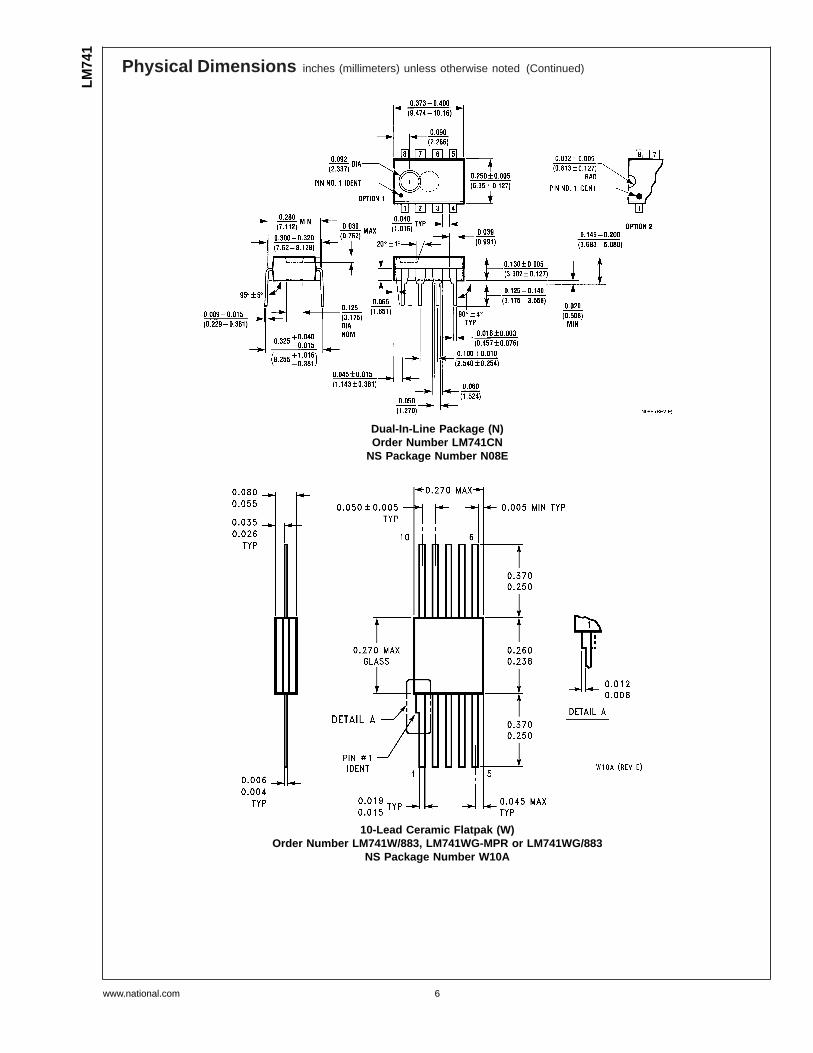
Physical Dimensions inches (millimeters) unless otherwise noted (Continued)
Dual-In-Line Package (N)Order Number LM741CN
NS Package Number N08E
10-Lead Ceramic Flatpak (W)Order Number LM741W/883, LM741WG-MPR or LM741WG/883
NS Package Number W10A
LM74
1
www.national.com 6

Notes
LIFE SUPPORT POLICY
NATIONAL’S PRODUCTS ARE NOT AUTHORIZED FOR USE AS CRITICAL COMPONENTS IN LIFE SUPPORTDEVICES OR SYSTEMS WITHOUT THE EXPRESS WRITTEN APPROVAL OF THE PRESIDENT AND GENERALCOUNSEL OF NATIONAL SEMICONDUCTOR CORPORATION. As used herein:
1. Life support devices or systems are devices orsystems which, (a) are intended for surgical implantinto the body, or (b) support or sustain life, andwhose failure to perform when properly used inaccordance with instructions for use provided in thelabeling, can be reasonably expected to result in asignificant injury to the user.
2. A critical component is any component of a lifesupport device or system whose failure to performcan be reasonably expected to cause the failure ofthe life support device or system, or to affect itssafety or effectiveness.
National SemiconductorCorporationAmericasTel: 1-800-272-9959Fax: 1-800-737-7018Email: [email protected]
National SemiconductorEurope
Fax: +49 (0) 180-530 85 86Email: [email protected]
Deutsch Tel: +49 (0) 69 9508 6208English Tel: +44 (0) 870 24 0 2171Français Tel: +33 (0) 1 41 91 8790
National SemiconductorAsia Pacific CustomerResponse GroupTel: 65-2544466Fax: 65-2504466Email: [email protected]
National SemiconductorJapan Ltd.Tel: 81-3-5639-7560Fax: 81-3-5639-7507
www.national.com
LM741
OperationalA
mplifier
National does not assume any responsibility for use of any circuitry described, no circuit patent licenses are implied and National reserves the right at any time without notice to change said circuitry and specifications.

1N/FD
LL 914/A/B
/ 916/A/B
/ 4148 / 4448
1N/FDLL 914/A/B / 916/A/B / 4148 / 4448
Small Signal DiodeAbsolute Maximum Ratings* TA = 25°C unless otherwise noted
*These ratings are limiting values above which the serviceability of any semiconductor device may be impaired.
NOTES:1) These ratings are based on a maximum junction temperature of 200 degrees C.2) These are steady state limits. The factory should be consulted on applications involving pulsed or low duty cycle operations.
Thermal Characteristics
2002 Fairchild Semiconductor Corporation
Symbol
Parameter
Value
Units VRRM Maximum Repetitive Reverse Voltage 100 V IF(AV) Average Rectified Forward Current 200 mA IFSM Non-repetitive Peak Forward Surge Current
Pulse Width = 1.0 second Pulse Width = 1.0 microsecond
1.0 4.0
A A
Tstg Storage Temperature Range -65 to +200 °C TJ Operating Junction Temperature 175 °C
Symbol
Characteristic
Max
Units 1N/FDLL 914/A/B / 4148 / 4448 PD Power Dissipation 500 mW RθJA Thermal Resistance, Junction to Ambient 300 °C/W
1N/FDLL 914/A/B / 916/A/B / 4148 / 4448, Rev. B

1N/FD
LL 914/A/B
/ 916/A/B
/ 4148 / 4448
Typical Characteristics
Small Signal Diode(continued)
Symbol
Parameter
Test Conditions
Min
Max
Units
VR Breakdown Voltage IR = 100 µA IR = 5.0 µA
100 75
V V
VF Forward Voltage 1N914B/4448 1N916B
1N914/916/4148 1N914A/916A
1N916B 1N914B/4448
IF = 5.0 mA IF = 5.0 mA IF = 10 mA IF = 20 mA IF = 20 mA IF = 100 mA
620 630
720 730 1.0 1.0 1.0 1.0
mV mV V V V V
IR Reverse Current VR = 20 V VR = 20 V, TA = 150°C VR = 75 V
25 50 5.0
nA µA µA
CT Total Capacitance 1N916A/B/4448 1N914A/B/4148
VR = 0, f = 1.0 MHz VR = 0, f = 1.0 MHz
2.0 4.0
pF pF
trr Reverse Recovery Time IF = 10 mA, VR = 6.0 V (60mA), Irr = 1.0 mA, RL = 100Ω
4.0 ns
Electrical Characteristics TA = 25°C unless otherwise noted
110
120
130
140
150
160Ta=25 oC
1 2 3 5 10 20 30 50 100
Rev
erse
Vol
tage
, V R
[V]
Reverse Current, IR [uA]
Figure 1. Reverse Voltage vs Reverse CurrentBV - 1.0 to 100 uA
0
20
40
60
80
100
120
10 20 30 50 70 100
Ta= 25 oC
Rev
erse
Cur
rent
, I
R [nA
]
Reverse Voltage, VR [V]
Figure 2. Reverse Current vs Reverse VoltageIR - 10 to 100 V
GENERAL RULE: The Reverse Current of a diode will approximatelydouble for every ten (10) Degree C increase in Temperature
250
300
350
400
450
500
550
1 2 3 5 10 20 30 50 100
Ta= 25 oC
Forw
ard
Volta
ge, V
R [m
V]
Forward Current, IF [uA]
Figure 3. Forward Voltage vs Forward CurrentVF - 1 to 100 uA
450
500
550
600
650
700
750
0.1 0.2 0.3 0.5 1 2 3 5 10
Ta= 25 oC
Forw
ard
Volta
ge, V
F [m
V]
Forward Current, IF [mA]Figure 4. Forward Voltage vs Forward Current
VF - 0.1 to 10 mA
1N/FD
LL 914/A/B
/ 916/A/B
/ 4148 / 4448
Typical Characteristics (continued)
Small Signal Diode(continued)
0 50 100 1500
100
200
300
400
500
IF(AV) - AVERAGE RECTIFIED CURRENT - mA
Cur
rent
(mA
)
Ambient Temperature ( oC)
0 2 4 6 8 10 12 140.75
0.80
0.85
0.90
TA = 25 oC
Tota
l Cap
acita
nce
(pF)
REVERSE VOLTAGE (V)
0.6
0.8
1.0
1.2
1.4
1.6
10 20 30 50 100 200 300 500 800
Ta= 25 oC
Forw
ard
Volta
ge, V
F [m
V]
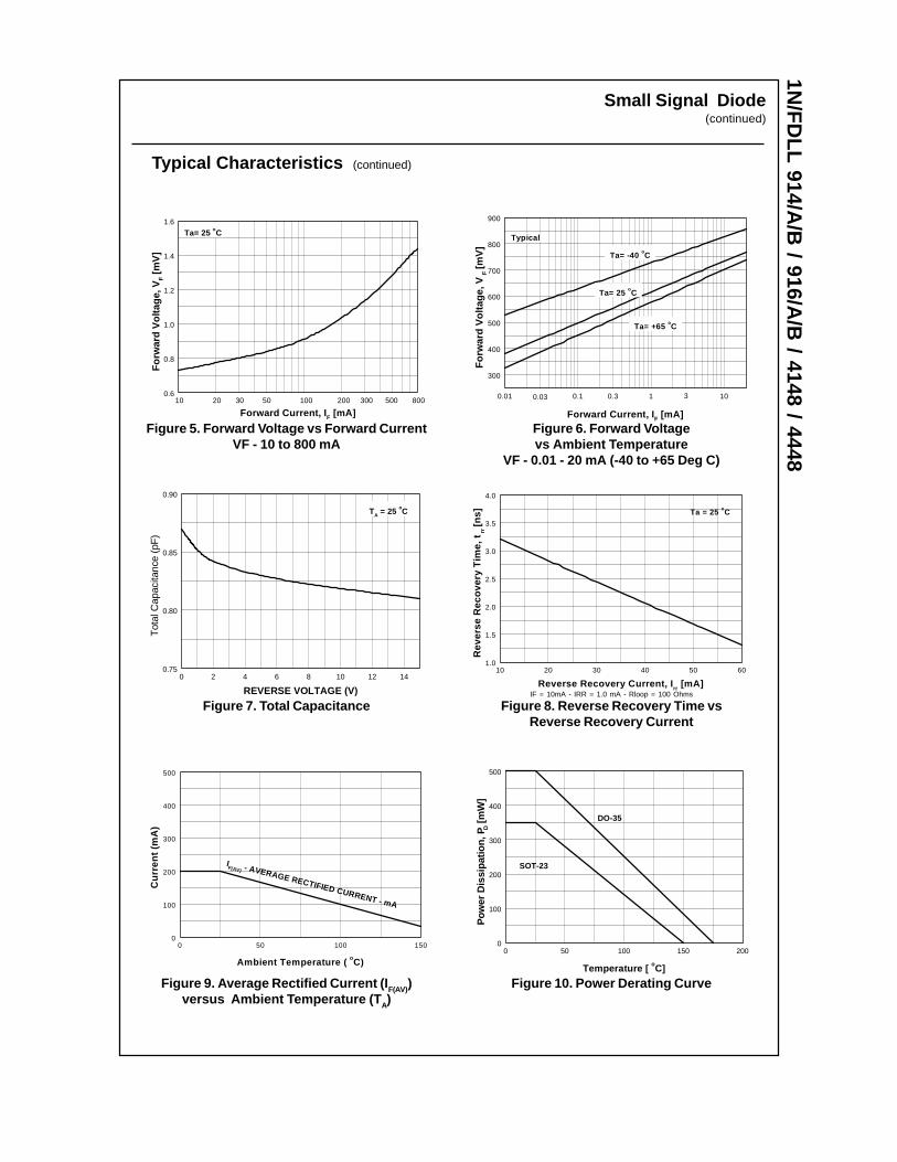
Forward Current, IF [mA]Figure 5. Forward Voltage vs Forward Current
VF - 10 to 800 mA
0.01 0.1 1 10
300
400
500
600
700
800
900
30.30.03
Typical
Ta= -40 oC
Ta= 25 oC
Ta= +65 oC
Forw
ard
Volta
ge, V
F [m
V]
Forward Current, IF [mA]Figure 6. Forward Voltagevs Ambient Temperature
VF - 0.01 - 20 mA (-40 to +65 Deg C)
10 20 30 40 50 601.0
1.5
2.0
2.5
3.0
3.5
4.0
Ta = 25 oC
Rev
erse
Rec
over
y Ti
me,
t
rr [ns]
Reverse Recovery Current, Irr [mA]
Figure 8. Reverse Recovery Time vsReverse Recovery Current
0 50 100 150 2000
100
200
300
400
500
DO-35
SOT-23
Pow
er D
issi
patio
n, P D [
mW
]
Temperature [ oC]Figure 10. Power Derating Curve
Figure 7. Total CapacitanceIF = 10mA - IRR = 1.0 mA - Rloop = 100 Ohms
Figure 9. Average Rectified Current (IF(AV))versus Ambient Temperature (TA)

!"#$%"&'(%& %)'"%&'!%*$%('((!'&$$%"'+'%,'*- %& ''.$'-'($$%+!% !"'*%("&%%$%%( /0!11 2 2345 123 4511 3 45 1 1 1 2 1 3 21 6 2
7 12111 2 1 21 11 23 2
$ 2
((
%
1 1 1122
1 2311 21 2 1
1 2 1
11 2 1 2
"
$
$
($
!" !
#$ !$% $&
'()!!*!* +
,$
" !
% -$"./".0".12 2, "$!$
8$%-'
3%3$45

November 1995
2N7000 / 2N7002 / NDS7002A N-Channel Enhancement Mode Field Effect Transistor
General Description Features
___________________________________________________________________________________________
Absolute Maximum Ratings TA = 25°C unless otherwise notedSymbol Parameter 2N7000 2N7002 NDS7002A Units
VDSS Drain-Source Voltage 60 V
VDGR Drain-Gate Voltage (RGS < 1 MΩ) 60 V
VGSS Gate-Source Voltage - Continuous ±20 V
- Non Repetitive (tp < 50µs) ±40
ID Maximum Drain Current - Continuous 200 115 280 mA - Pulsed 500 800 1500
PD Maximum Power Dissipation 400 200 300 mW
Derated above 25oC 3.2 1.6 2.4 mW/°CTJ,TSTG Operating and Storage Temperature Range -55 to 150 -65 to 150 °C
TL Maximum Lead Temperature for SolderingPurposes, 1/16" from Case for 10 Seconds
300 °C
THERMAL CHARACTERISTICS
RθJAThermal Resistance, Junction-to-Ambient 312.5 625 417 °C/W
2N7000.SAM Rev. A1
These N-Channel enhancement mode field effect transistorsare produced using Fairchild's proprietary, high cell density,DMOS technology. These products have been designed tominimize on-state resistance while provide rugged, reliable,and fast switching performance. They can be used in mostapplications requiring up to 400mA DC and can deliverpulsed currents up to 2A. These products are particularlysuited for low voltage, low current applications such as smallservo motor control, power MOSFET gate drivers, and otherswitching applications.
High density cell design for low RDS(ON).
Voltage controlled small signal switch.
Rugged and reliable.
High saturation current capability.
S
D
G
SG
D
TO-92
© 1997 Fairchild Semiconductor Corporation
2N7000 (TO-236AB)
2N7002/NDS7002A

Electrical Characteristics TA = 25°C unless otherwise noted
Symbol Parameter Conditions Type Min Typ Max Units
OFF CHARACTERISTICS
BVDSS Drain-Source Breakdown Voltage VGS = 0 V, ID = 10 µA All 60 V
IDSS Zero Gate Voltage Drain Current VDS = 48 V, VGS = 0 V 2N7000 1 µA
TJ=125°C 1 mAVDS = 60 V, VGS = 0 V 2N7002
NDS7002A1 µA
TJ=125°C 0.5 mAIGSSF Gate - Body Leakage, Forward VGS = 15 V, VDS = 0 V 2N7000 10 nA
VGS = 20 V, VDS = 0 V 2N7002NDS7002A
100 nA
IGSSR Gate - Body Leakage, Reverse VGS = -15 V, VDS = 0 V 2N7000 -10 nAVGS = -20 V, VDS = 0 V 2N7002
NDS7002A-100 nA
ON CHARACTERISTICS (Note 1)
VGS(th) Gate Threshold Voltage VDS = VGS, ID = 1 mA 2N7000 0.8 2.1 3 V
VDS = VGS, ID = 250 µA 2N7002NDS7002A
1 2.1 2.5
RDS(ON) Static Drain-Source On-Resistance VGS = 10 V, ID = 500 mA 2N7000 1.2 5 ΩTJ =125°C 1.9 9
VGS = 4.5 V, ID = 75 mA 1.8 5.3VGS = 10 V, ID = 500 mA 2N7002 1.2 7.5
TJ =100°C 1.7 13.5VGS = 5.0 V, ID = 50 mA 1.7 7.5
TJ =100C 2.4 13.5VGS = 10 V, ID = 500 mA NDS7002A 1.2 2
TJ =125°C 2 3.5VGS = 5.0 V, ID = 50 mA 1.7 3
TJ =125°C 2.8 5VDS(ON) Drain-Source On-Voltage VGS = 10 V, ID = 500 mA 2N7000 0.6 2.5 V
VGS = 4.5 V, ID = 75 mA 0.14 0.4VGS = 10 V, ID = 500mA 2N7002 0.6 3.75VGS = 5.0 V, ID = 50 mA 0.09 1.5VGS = 10 V, ID = 500mA NDS7002A 0.6 1VGS = 5.0 V, ID = 50 mA 0.09 0.15
2N7000.SAM Rev. A1
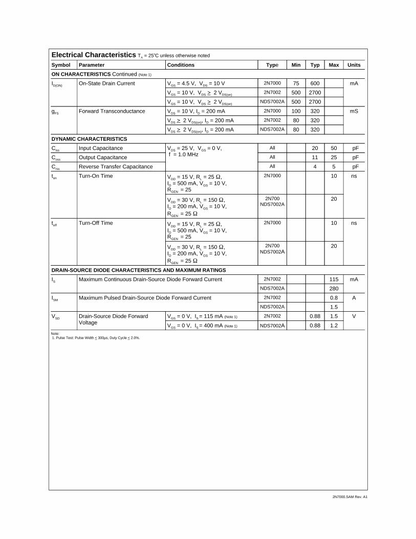
Electrical Characteristics TA = 25oC unless otherwise noted
Symbol Parameter Conditions Type Min Typ Max UnitsON CHARACTERISTICS Continued (Note 1)
ID(ON) On-State Drain Current VGS = 4.5 V, VDS = 10 V 2N7000 75 600 mAVGS = 10 V, VDS > 2 VDS(on) 2N7002 500 2700VGS = 10 V, VDS > 2 VDS(on) NDS7002A 500 2700
gFS Forward Transconductance VDS = 10 V, ID = 200 mA 2N7000 100 320 mSVDS > 2 VDS(on), ID = 200 mA 2N7002 80 320VDS > 2 VDS(on), ID = 200 mA NDS7002A 80 320
DYNAMIC CHARACTERISTICSCiss Input Capacitance VDS = 25 V, VGS = 0 V,
f = 1.0 MHzAll 20 50 pF
Coss Output Capacitance All 11 25 pFCrss Reverse Transfer Capacitance All 4 5 pFton Turn-On Time VDD = 15 V, RL = 25 Ω,
ID = 500 mA, VGS = 10 V, RGEN = 25
2N7000 10 ns
VDD = 30 V, RL = 150 Ω,ID = 200 mA, VGS = 10 V,RGEN = 25 Ω
2N700NDS7002A
20
toff Turn-Off Time VDD = 15 V, RL = 25 Ω, ID = 500 mA, VGS = 10 V, RGEN = 25
2N7000 10 ns
VDD = 30 V, RL = 150 Ω,ID = 200 mA, VGS = 10 V,RGEN = 25 Ω
2N700NDS7002A
20
DRAIN-SOURCE DIODE CHARACTERISTICS AND MAXIMUM RATINGSIS Maximum Continuous Drain-Source Diode Forward Current 2N7002 115 mA
NDS7002A 280ISM Maximum Pulsed Drain-Source Diode Forward Current 2N7002 0.8 A
NDS7002A 1.5VSD Drain-Source Diode Forward
VoltageVGS = 0 V, IS = 115 mA (Note 1) 2N7002 0.88 1.5 VVGS = 0 V, IS = 400 mA (Note 1) NDS7002A 0.88 1.2
Note:1. Pulse Test: Pulse Width < 300µs, Duty Cycle < 2.0%.
2N7000.SAM Rev. A1

2N7000.SAM Rev. A1
0 1 2 3 4 50
0.5
1
1.5
2
V , DRAIN-SOURCE VOLTAGE (V)
I ,
DR
AIN
-SO
UR
CE
CU
RR
ENT
(A)
9.0
4.0
8.0
3.0
7.0
V = 10VGS
DS
D
5.0
6.0
-50 -25 0 25 50 75 100 125 1500.5
0.75
1
1.25
1.5
1.75
2
T , JUNCTION TEMPERATURE (°C)
DR
AIN
-SO
UR
CE
ON
-RES
ISTA
NC
E
J
R
, N
OR
MAL
IZED
DS(
ON
)
V = 10VGSI = 500m AD
-50 -25 0 25 50 75 100 125 1500.8
0.85
0.9
0.95
1
1.05
1.1
T , JUNCTION TEM PERATURE (°C)
GAT
E-SO
UR
CE
THR
ESH
OLD
VO
LTAG
E
J
I = 1 m AD
V = VDS GS
V ,
NO
RM
ALIZ
EDth
0 0.4 0.8 1.2 1.6 20.5
1
1.5
2
2.5
3
I , DRA IN CURRENT (A)
DR
AIN
-SO
UR
CE
ON
-RES
ISTA
NC
E
V =4.0V GS
D
R
, N
OR
MAL
IZED
DS(
on)
7.0
4.5
10
5.0
6.0
9.08.0
0 0.4 0.8 1.2 1.6 20
0.5
1
1.5
2
2.5
3
I , DRAIN CURRENT (A)
DR
AIN
-SO
UR
CE
ON
-RES
ISTA
NC
E
T = 125°CJ
25°C
-55°C
D
V = 10V GS
R
, N
OR
MAL
IZED
DS(
on)
Typical Electrical Characteristics
Figure 1. On-Region Characteristics Figure 2. On-Resistance Variation with GateVoltage and Drain Current
Figure 3. On-Resistance Variationwith Temperature
Figure 4. On-Resistance Variation with DrainCurrent and Temperature
Figure 5. Transfer Characteristics Figure 6. Gate Threshold Variation withTemperature
0 2 4 6 8 100
0.4
0.8
1.2
1.6
2
V , GATE TO SOURCE VOLTAGE (V)
I ,
DR
AIN
CU
RR
ENT
(A)
V = 10VDS
GS
D
T = -55°CJ 25°C125°C
2N7000 / 2N7002 / NDS7002A

2N7000.SAM Rev. A1
-50 -25 0 25 50 75 100 125 1500.925
0.95
0.975
1
1.025
1.05
1.075
1.1
T , JUNCTION TEM PERATURE (°C)
DR
AIN
-SO
UR
CE
BREA
KDO
WN
VO
LTAG
E
J
BV
,
NO
RM
ALIZ
EDD
SS
I = 250µAD
0.2 0.4 0.6 0.8 1 1.2 1.40.001
0.005
0.01
0.05
0.1
0.5
1
2
V , BODY DIODE FORWARD VOLTAGE (V)
I ,
REV
ERSE
DR
AIN
CU
RR
ENT
(A)
V = 0VGS
T = 125°CJ
SD
S
25°C
-55°C
0 0.4 0.8 1.2 1.6 20
2
4
6
8
10
Q , GATE CHARGE (nC)
V
, G
ATE-
SOU
RC
E VO
LTAG
E (V
)
g
GS
I =500m AD
V = 25VDS
115m A
280m A
1 2 3 5 10 20 30 501
2
5
10
20
40
60
V , DRAIN TO SOURCE VOLTAGE (V)
CAP
ACIT
ANC
E (p
F)
DS
C iss
f = 1 MHzV = 0VGS
C oss
C rss
G
D
S
VDD
R LV
V
IN
OUT
VGSDUTRGEN
10%
50%
90%
10%
90%
90%
50%Input, Vin
Output, Vout
t on toff
td(off) t ftrt d(on)
Inverted10%
Pulse Width
Figure 7. Breakdown Voltage Variationwith Temperature
Figure 8. Body Diode Forward Voltage Variation with
Figure 9. Capacitance Characteristics Figure 10. Gate Charge Characteristics
Figure 11. Figure 12. Switching Waveforms
Typical Electrical Characteristics (continued)2N7000 / 2N7002 /NDS7002A

2N7000.SAM Rev. A1
0.0001 0.001 0.01 0.1 1 10 100 3000.001
0.002
0.01
0.05
0.1
0.2
0.5
1
t , TIME (sec)
TR
AN
SIE
NT
TH
ER
MA
L R
ES
ISTA
NC
Er(
t), N
OR
MA
LIZ
ED
EF
FE
CT
IVE
1
Single Pulse
D = 0.5
0.1
0 .05
0 .02
0 .01
0 .2
Duty Cycle, D = t /t1 2
R (t) = r(t) * R R = (See Datasheet)
θJAθJAθJA
T - T = P * R (t)θJAAJ
P(pk)
t 1 t 2
0.0001 0.001 0.01 0.1 1 10 100 3000.01
0.02
0.05
0.1
0.2
0.5
1
t , TIME (sec)
TR
AN
SIE
NT
TH
ER
MA
L R
ES
ISTA
NC
Er(
t), N
OR
MA
LIZ
ED
EF
FE
CT
IVE
1
Single Pulse
D = 0.5
0.1
0.05
0 .02
0.01
0 .2
Duty Cycle, D = t /t1 2
R (t) = r(t) * R R = (See Datasheet)
θJAθJAθJA
T - T = P * R (t)θJAAJ
P(pk)
t 1 t 2
1 2 5 10 20 30 60 800.005
0.01
0.05
0.1
0.5
1
23
V , DRAIN-SOURCE VOLTAGE (V)
I ,
DR
AIN
CU
RR
ENT
(A)
DS
D
V = 10VSINGLE PULSE
T = 25°C
GS
A
RDS(ON) Lim it
100m s
1ms10m s
DC
1s
100us
10s
Figure 16. TO-92, 2N7000 Transient Thermal Response Curve
Figure 17. SOT-23, 2N7002 / NDS7002A Transient Thermal Response Curve
1 2 5 10 20 30 60 800.005
0.01
0.05
0.1
0.5
1
23
V , DRAIN-SOURCE VOLTAGE (V)
I ,
DR
AIN
CU
RR
ENT
(A)
DS
D
V = 10VSINGLE PULSE
T = 25°C
GS
A
RDS(ON) Lim it
100m s
1ms
10m s
DC
1s10s
100us
1 2 5 10 20 30 60 800.005
0.01
0.05
0.1
0.5
1
23
V , DRAIN-SOURCE VOLTAGE (V)
I ,
DR
AIN
CU
RR
ENT
(A)
DS
D V = 10VSINGLE PULSE
T = 25°C
GS
A
RDS(ON) Lim it
100m s
1ms
10m s
DC
1s10s
100us
Figure 13. 2N7000 MaximumSafe Operating Area
Figure 14. 2N7002 MaximumSafe Operating Area
Figure 15. NDS7000A MaximumSafe Operating Area
Typical Electrical Characteristics (continued)

TRADEMARKSThe following are registered and unregistered trademarks Fairchild Semiconductor owns or is authorized to use and isnot intended to be an exhaustive list of all such trademarks.
LIFE SUPPORT POLICY
FAIRCHILD’S PRODUCTS ARE NOT AUTHORIZED FOR USE AS CRITICAL COMPONENTS IN LIFE SUPPORTDEVICES OR SYSTEMS WITHOUT THE EXPRESS WRITTEN APPROVAL OF FAIRCHILD SEMICONDUCTOR CORPORATION.As used herein:1. Life support devices or systems are devices orsystems which, (a) are intended for surgical implant intothe body, or (b) support or sustain life, or (c) whosefailure to perform when properly used in accordancewith instructions for use provided in the labeling, can bereasonably expected to result in significant injury to theuser.
2. A critical component is any component of a lifesupport device or system whose failure to perform canbe reasonably expected to cause the failure of the lifesupport device or system, or to affect its safety oreffectiveness.
PRODUCT STATUS DEFINITIONS
Definition of Terms
Datasheet Identification Product Status Definition
Advance Information
Preliminary
No Identification Needed
Obsolete
This datasheet contains the design specifications forproduct development. Specifications may change inany manner without notice.
This datasheet contains preliminary data, andsupplementary data will be published at a later date.Fairchild Semiconductor reserves the right to makechanges at any time without notice in order to improvedesign.
This datasheet contains final specifications. FairchildSemiconductor reserves the right to make changes atany time without notice in order to improve design.
This datasheet contains specifications on a productthat has been discontinued by Fairchild semiconductor.The datasheet is printed for reference information only.
Formative orIn Design
First Production
Full Production
Not In Production
DISCLAIMER
FAIRCHILD SEMICONDUCTOR RESERVES THE RIGHT TO MAKE CHANGES WITHOUT FURTHERNOTICE TO ANY PRODUCTS HEREIN TO IMPROVE RELIABILITY, FUNCTION OR DESIGN. FAIRCHILDDOES NOT ASSUME ANY LIABILITY ARISING OUT OF THE APPLICATION OR USE OF ANY PRODUCTOR CIRCUIT DESCRIBED HEREIN; NEITHER DOES IT CONVEY ANY LICENSE UNDER ITS PATENTRIGHTS, NOR THE RIGHTS OF OTHERS.
PowerTrenchQFET™QS™QT Optoelectronics™Quiet Series™SILENT SWITCHERSMART START™SuperSOT™-3SuperSOT™-6SuperSOT™-8
FASTr™GlobalOptoisolator™GTO™HiSeC™ISOPLANAR™MICROWIRE™OPTOLOGIC™OPTOPLANAR™PACMAN™POP™
Rev. G
ACEx™Bottomless™CoolFET™CROSSVOLT™DOME™E2CMOSTM
EnSignaTM
FACT™FACT Quiet Series™FAST
SyncFET™TinyLogic™UHC™VCX™

2N2219A2N2222A
HIGH SPEED SWITCHESPRELIMINARY DATA
DESCRIPTION The 2N2219A and 2N2222A are silicon PlanarEpitaxial NPN transistors in Jedec TO-39 (for2N2219A) and in Jedec TO-18 (for 2N2222A)metal case. They are designed for high speedswitching application at collector current up to500mA, and feature useful current gain over awide range of collector current, low leakagecurrents and low saturation voltage.
®
INTERNAL SCHEMATIC DIAGRAM
February 2003
ABSOLUTE MAXIMUM RATINGS
Symbol Parameter Value Unit
VCBO Collector-Base Voltage (IE = 0) 75 V
VCEO Collector-Emitter Voltage (IB = 0) 40 V
VEBO Emitter-Base Voltage (IC = 0) 6 V
IC Collector Current 0.6 A
ICM Collector Peak Current (tp < 5 ms) 0.8 A
Ptot Total Dissipation at Tamb ≤ 25 oC for 2N2219A for 2N2222A at TC ≤ 25 oC for 2N2219A for 2N2222A
0.80.5
31.8
WW
WW
Tstg Storage Temperature -65 to 175 oC
Tj Max. Operating Junction Temperature 175 oC
TO-18 TO-39
1/7

THERMAL DATA
TO-39 TO-18
Rthj-case
Rthj-amb
Thermal Resistance Junction-Case MaxThermal Resistance Junction-Ambient Max
50187.5
83.3300
oC/WoC/W
ELECTRICAL CHARACTERISTICS (Tcase = 25 oC unless otherwise specified)
Symbol Parameter Test Conditions Min. Typ. Max. Unit
ICBO Collector Cut-offCurrent (IE = 0)
VCB = 60 VVCB = 60 V Tj = 150 oC
1010
nAµA
ICEX Collector Cut-offCurrent (VBE = -3V)
VCE = 60 V 10 nA
IBEX Base Cut-off Current(VBE = -3V)
VCE = 60 V 20 nA
IEBO Emitter Cut-off Current(IC = 0)
VEB = 3 V 10 nA
V(BR)CBO Collector-BaseBreakdown Voltage(IE = 0)
IC = 10 µA 75 V
V(BR)CEO∗ Collector-EmitterBreakdown Voltage(IB = 0)
IC = 10 mA 40 V
V(BR)EBO Emitter-BaseBreakdown Voltage(IC = 0)
IE = 10 µA 6 V
VCE(sat)∗ Collector-EmitterSaturation Voltage
IC = 150 mA IB = 15 mAIC = 500 mA IB = 50 mA
0.31
VV
VBE(sat)∗ Base-EmitterSaturation Voltage
IC = 150 mA IB = 15 mAIC = 500 mA IB = 50 mA
0.6 1.22
VV
hFE∗ DC Current Gain IC = 0.1 mA VCE = 10 VIC = 1 mA VCE = 10 VIC = 10 mA VCE = 10 VIC = 150 mA VCE = 10 VIC = 500 mA VCE = 10 VIC = 150 mA VCE = 1 VIC = 10 mA VCE = 10 V Tamb = -55 oC
355075
1004050
35
300
hfe∗ Small Signal CurrentGain
IC = 1 mA VCE = 10 V f = 1KHzIC = 10 mA VCE = 10 V f = 1KHz
5075
300375
fT Transition Frequency IC = 20 mA VCE = 20 V f = 100 MHz
300 MHz
CEBO Emitter-BaseCapacitance
IC = 0 VEB = 0.5 V f = 100KHz 25 pF
CCBO Collector-BaseCapacitance
IE = 0 VCB = 10 V f = 100 KHz 8 pF
Re(hie) Real Part of InputImpedance
IC = 20 mA VCE = 20 V f = 300MHz
60 Ω
* Pulsed: Pulse duration = 300 µs, duty cycle ≤ 1 %
2N2219A / 2N2222A
2/7

ELECTRICAL CHARACTERISTICS (continued)
Symbol Parameter Test Conditions Min. Typ. Max. Unit
NF Noise Figure IC = 0.1 mA VCE = 10 V f = 1KHz Rg = 1KΩ
4 dB
hie Input Impedance IC = 1 mA VCE = 10 VIC = 10 mA VCE = 10 V
20.25
81.25
kΩkΩ
hre Reverse Voltage Ratio IC = 1 mA VCE = 10 VIC = 10 mA VCE = 10 V
84
10-4
10-4
hoe Output Admittance IC = 1 mA VCE = 10 VIC = 10 mA VCE = 10 V
525
35200
µSµS
td∗∗ Delay Time VCC = 30 V IC = 150 mA IB1 = 15 mA VBB = -0.5 V
10 ns
tr∗∗ Rise Time VCC = 30 V IC = 150 mA IB1 = 15 mA VBB = -0.5 V
25 ns
ts∗∗ Storage Time VCC = 30 V IC = 150 mA IB1 = -IB2 = 15 mA
225 ns
tf∗∗ Fall Time VCC = 30 V IC = 150 mA IB1 = -IB2 = 15 mA
60 ns
rbb’ Cb’c Feedback TimeConstant
IC = 20 mA VCE = 20 V f = 31.8MHz
150 ps
∗ Pulsed: Pulse duration = 300 µs, duty cycle ≤ 1 %∗∗ See test circuit
2N2219A / 2N2222A
3/7

Test Circuit fot td, tr.
PULSE GENERATOR : TO OSCILLOSCOPE tr ≤ 20 ns tr ≤ 5.0 nsPW ≤ 200 ns ZIN < 100 KΩZIN = 50 Ω CIN ≤ 12 pF
Test Circuit fot td, tr.
PULSE GENERATOR : TO OSCILLOSCOPE :PW ≈ 10 µs tr < 5.0 nsZIN = 50 Ω ZIN > 100 KΩTC ≤ 5.0 ns CIN ≤ 12 pF
2N2219A / 2N2222A
4/7

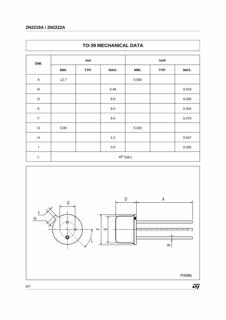
DIM.mm inch
MIN. TYP. MAX. MIN. TYP. MAX.
A 12.7 0.500
B 0.49 0.019
D 5.3 0.208
E 4.9 0.193
F 5.8 0.228
G 2.54 0.100
H 1.2 0.047
I 1.16 0.045
L 45o 45o
L
G
I
D A
F E
B
H
C
TO-18 MECHANICAL DATA
0016043
2N2219A / 2N2222A
5/7
DIM.mm inch
MIN. TYP. MAX. MIN. TYP. MAX.
A 12.7 0.500
B 0.49 0.019
D 6.6 0.260
E 8.5 0.334
F 9.4 0.370
G 5.08 0.200
H 1.2 0.047
I 0.9 0.035
L 45o (typ.)
L
G
I
D A
F E
B
H
P008B
TO-39 MECHANICAL DATA
2N2219A / 2N2222A
6/7
Information furnished is believed to be accurate and reliable. However, STMicroelectronics assumes no responsibility for the consequencesof use of such information nor for any infringement of patents or other rights of third parties which may result from its use. No license isgranted by implication or otherwise under any patent or patent rights of STMicroelectronics. Specification mentioned in this publication aresubject to change without notice. This publication supersedes and replaces all information previously supplied. STMicroelectronics productsare not authorized for use as critical components in life support devices or systems without express written approval of STMicroelectronics.
The ST logo is a trademark of STMicroelectronics
© 2003 STMicroelectronics – Printed in Italy – All Rights ReservedSTMicroelectronics GROUP OF COMPANIES
Australia - Brazil - Canada - China - Finland - France - Germany - Hong Kong - India - Israel - Italy - Japan - Malaysia - Malta - Morocco - Singapore - Spain - Sweden - Switzerland - United Kingdom - United States.
http://www.st.com
2N2219A / 2N2222A
7/7

DATA SHEET
Product specificationSupersedes data of September 1994File under Discrete Semiconductors, SC04
1997 May 30
DISCRETE SEMICONDUCTORS
2N2907; 2N2907APNP switching transistors
M3D125

1997 May 30 2
Philips Semiconductors Product specification
PNP switching transistors 2N2907; 2N2907A
FEATURES
• High current (max. 600 mA)
• Low voltage (max. 60 V).
APPLICATIONS
• Switching and linear amplification.
DESCRIPTION
PNP switching transistor in a TO-18 metal package.NPN complements: 2N2222 and 2N2222A.
PINNING
PIN DESCRIPTION
1 emitter
2 base
3 collector, connected to case
Fig.1 Simplified outline (TO-18) and symbol.
handbook, halfpage
MAM2631
3
2
3
12
QUICK REFERENCE DATA
SYMBOL PARAMETER CONDITIONS MIN. MAX. UNIT
VCBO collector-base voltage open emitter − −60 V
VCEO collector-emitter voltage open base
2N2907 − −40 V
2N2907A − −60 V
IC collector current (DC) − −600 mA
Ptot total power dissipation Tamb ≤ 25 °C − 400 mW
hFE DC current gain IC = −150 mA; VCE = −10 V 100 300
fT transition frequency IC = −50 mA; VCE = −20 V; f = 100 MHz 200 − MHz
toff turn-off time ICon = −150 mA; IBon = −15 mA; IBoff = 15 mA − 300 ns

1997 May 30 3
Philips Semiconductors Product specification
PNP switching transistors 2N2907; 2N2907A
LIMITING VALUESIn accordance with the Absolute Maximum Rating System (IEC 134).
THERMAL CHARACTERISTICS
SYMBOL PARAMETER CONDITIONS MIN. MAX. UNIT
VCBO collector-base voltage open emitter − −60 V
VCEO collector-emitter voltage open base; IC < −100 mA
2N2907 − −40 V
2N2907A − −60 V
VEBO emitter-base voltage open collector − −5 V
IC collector current (DC) − −600 mA
ICM peak collector current − −800 mA
IBM peak base current − −200 mA
Ptot total power dissipation Tamb ≤ 25 °C − 400 mW
Tcase ≤ 25 °C − 1.2 W
Tstg storage temperature −65 +150 °CTj junction temperature − 200 °CTamb operating ambient temperature −65 +150 °C
SYMBOL PARAMETER CONDITIONS VALUE UNIT
Rth j-a thermal resistance from junction to ambient in free air 438 K/W
Rth j-c thermal resistance from junction to case 146 K/W

1997 May 30 4
Philips Semiconductors Product specification
PNP switching transistors 2N2907; 2N2907A
CHARACTERISTICSTamb = 25 °C unless otherwise specified.
Note
1. Pulse test: tp ≤ 300 µs; δ ≤ 0.02.
SYMBOL PARAMETER CONDITIONS MIN. MAX. UNIT
ICBO collector cut-off current
2N2907 IE = 0; VCB = −50 V − −20 nA
IE = 0; VCB = −50 V; Tamb = 150 °C − −20 µA
ICBO collector cut-off current
2N2907A IE = 0; VCB = −50 V − −10 nA
IE = 0; VCB = −50 V; Tamb = 150 °C − −10 µA
IEBO emitter cut-off current IC = 0; VEB = −5 V − −50 nA
hFE DC current gain VCE = −10 V
2N2907 IC = −0.1 mA 35 −IC = −1 mA 50 −IC = −10 mA 75 −IC = −150 mA; note 1 100 300
IC = −500 mA; note 1 30
hFE DC current gain VCE = −10 V
2N2907A IC = −0.1 mA 75 −IC = −1 mA 100 −IC = −10 mA 100 −IC = −150 mA; note 1 100 300
IC = −500 mA; note 1 50 −VCEsat collector-emitter saturation voltage IC = −150 mA; IB = −15 mA; note 1 −400 mV
IC = −500 mA; IB = −50 mA; note 1 −1.6 V
VBEsat base-emitter saturation voltage IC = −150 mA; IB = −15 mA; note 1 −1.3 V
IC = −500 mA; IB = −50 mA; note 1 −2.6 V
Cc collector capacitance IE = ie = 0; VCB = −10 V; f = 1 MHz − 8 pF
Ce emitter capacitance IC = ic = 0; VEB = −2 V; f = 1 MHz − 30 pF
fT transition frequency IC = −50 mA; VCE = −20 V; f = 100 MHz;note 1
200 − MHz
Switching times (between 10% and 90% levels); see Fig.2
ton turn-on time ICon = −150 mA; IBon = −15 mA; IBoff = 15 mA − 45 ns
td delay time − 15 ns
tr rise time − 35 ns
toff turn-off time − 300 ns
ts storage time − 250 ns
tf fall time − 50 ns

1997 May 30 5
Philips Semiconductors Product specification
PNP switching transistors 2N2907; 2N2907A
Fig.2 Test circuit for switching times.
handbook, full pagewidth
RC
R2
R1
DUT
MGD624
Vo
RB(probe)
450 Ω(probe)
450 Ωoscilloscope oscilloscope
VBB
Vi
VCC
Vi = −9.5 V; T = 500 µs; tp = 10 µs; tr = tf ≤ 3 ns.
R1 = 68 Ω; R2 = 325 Ω; RB = 325 Ω; RC = 160 Ω.
VBB = 3.5 V; VCC = −29.5 V.
Oscilloscope input impedance Zi = 50 Ω.

1997 May 30 6
Philips Semiconductors Product specification
PNP switching transistors 2N2907; 2N2907A
PACKAGE OUTLINE
REFERENCESOUTLINEVERSION
EUROPEANPROJECTION ISSUE DATE
IEC JEDEC EIAJ
SOT18/13 TO-18B11/C7 type 3 97-04-18
a
α
k
D A L
seating plane
b
D1
0 5 10 mm
scale
Metal-can cylindrical single-ended package; 3 leads SOT18/13
w AM M B M
A
1
2
3
j
B
DIMENSIONS (millimetre dimensions are derived from the original inch dimensions)
UNIT w
mm 5.314.74
0.470.41
5.455.30
4.704.55
1.030.94
1.10.9
15.012.7
α
0.40 45°
A a b D D1 j k L
2.54

1997 May 30 7
Philips Semiconductors Product specification
PNP switching transistors 2N2907; 2N2907A
DEFINITIONS
LIFE SUPPORT APPLICATIONS
These products are not designed for use in life support appliances, devices, or systems where malfunction of theseproducts can reasonably be expected to result in personal injury. Philips customers using or selling these products foruse in such applications do so at their own risk and agree to fully indemnify Philips for any damages resulting from suchimproper use or sale.
Data sheet status
Objective specification This data sheet contains target or goal specifications for product development.
Preliminary specification This data sheet contains preliminary data; supplementary data may be published later.
Product specification This data sheet contains final product specifications.
Limiting values
Limiting values given are in accordance with the Absolute Maximum Rating System (IEC 134). Stress above one ormore of the limiting values may cause permanent damage to the device. These are stress ratings only and operationof the device at these or at any other conditions above those given in the Characteristics sections of the specificationis not implied. Exposure to limiting values for extended periods may affect device reliability.
Application information
Where application information is given, it is advisory and does not form part of the specification.

October 1987
Revised January 1999
CD
4007C D
ual C
om
plem
entary P
air Plu
s Inverter
© 1999 Fairchild Semiconductor Corporation DS005943.prf www.fairchildsemi.com
CD4007CDual Complementary Pair Plus Inverter
General DescriptionThe CD4007C consists of three complementary pairs of N-and P-channel enhancement mode MOS transistors suit-able for series/shunt applications. All inputs are protectedfrom static discharge by diode clamps to VDD and VSS.
For proper operation the voltages at all pins must be con-strained to be between VSS − 0.3V and VDD + 0.3V at alltimes.
Features Wide supply voltage range: 3.0V to 15V
High noise immunity: 0.45 VCC (typ.)
Ordering Code:
Devices also available in Tape and Reel. Specify by appending the suffix letter “X” to the ordering code.
Connection Diagram
Pin Assignments for DIP and SOIC
Note: All P-channel substrates are connected to VDD and all N-channel substrates are connected to VSS.
Top View
Order Number Package Number Package Description
CD4007CM M14A 14-Lead Small Outline Integrated Circuit (SOIC), JEDEC MS-120, 0.150” Narrow
CD4007CN N14A 14-Lead Plastic Dual-In-Line Package (PDIP), JEDEC MS–001, 0.300” Wide

www.fairchildsemi.com 2
CD
4007
CAbsolute Maximum Ratings(Note 1)
Note 1: This device should not be connected to circuits with the power onbecause high transient voltages may cause permanent damage.
DC Electrical Characteristics
AC Electrical Characteristics (Note 2)
TA = 25°C and CL = 15 pF and rise and fall times = 20 ns. Typical temperature coefficient for all values of VDD = 0.3%/°C
Note 2: AC Parameters are guaranteed by DC correlated testing.
Voltage at Any Pin VSS −0.3V to VDD +0.3V
Operating Temperature Range −40°C to +85°CStorage Temperature Range −65°C to +150°CPower Dissipation (PD)
Dual-In-Line 700 mW
Small Outline 500 mW
Operating VDD Range VSS +3.0V to VSS +15V
Lead Temperature
(Soldering, 10 seconds) 260°C
Limits
Symbol Parameter Conditions −40°C +25°C +85°C Units
Min Typ Max Min Typ Max Min Typ Max
IL Quiescent Device VDD = 5.0V 0.5 0.005 0.05 15 µA
Current VDD = 10V 1.0 0.005 1.0 30 µA
PD Quiescent Device VDD = 5.0V 2.5 0.025 2.5 75 µW
Dissipation Package VDD = 10V 10 0.05 10 300 µW
VOL Output Voltage VDD = 5.0V 0.05 0 0.01 0.05 V
LOW Level VDD = 10V 0.05 0 0.01 0.05 V
VOH Output Voltage VDD = 5.0V 4.95 4.95 5.0 4.95 V
HIGH Level VDD = 10V 9.95 9.95 10 9.95 V
VNL Noise Immunity VDD = 5.0V, VO = 3.6V 1.5 2.25 1.5 1.4 V
(All inputs) VDD = 10V, VO = 7.2V 3.0 4.5 3.0 2.9 V
VNH Noise Immunity VDD = 5.0V, VO = 0.95V 3.6 3.5 2.25 3.5 V
(All Inputs) VDD = 10V, VO = 2.9V 7.1 7.0 4.5 7.0 V
IDN Output Drive Current VDD = 5.0V, VO = 0.4V, VI = VDD 0.35 0.3 1.0 0.24 mA
N-Channel VDD = 10V, VO = 0.5V, VI = VDD 1.2 1.0 2.5 0.8 mA
IDP Output Drive Current VDD = 5.0V, VO = 2.5V, VI = VSS −1.3 −1.1 −4.0 −0.9 mA
P-Channel VDD = 10V, VO = 9.5V, VI = VSS −0.65 −0.55 −2.5 −0.45 mA
II Input Current 10 pA
Symbol Parameter Conditions Min Typ Max Units
tPLH = tPHL Propagation Delay Time VDD = 5.0V 35 75 ns
VDD = 10V 20 50 ns
tTLH = tTHL Transition Time VDD = 5.0V 50 100 ns
VDD = 10V 30 50 ns
CI Input Capacitance Any Input 5 pF

3 www.fairchildsemi.com
CD
4007C
AC Test Circuits
Switching Time Waveforms

www.fairchildsemi.com 4
CD
4007
CPhysical Dimensions inches (millimeters) unless otherwise noted
14-Lead Small Outline Integrated Circuit (SOIC), JEDEC MS-120, 0.150” NarrowPackage Number M14A

Fairchild does not assume any responsibility for use of any circuitry described, no circuit patent licenses are implied and Fairchild reserves the right at any time without notice to change said circuitry and specifications.
CD
4007C D
ual C
om
plem
entary P
air Plu
s Inverter
LIFE SUPPORT POLICY
FAIRCHILD’S PRODUCTS ARE NOT AUTHORIZED FOR USE AS CRITICAL COMPONENTS IN LIFE SUPPORTDEVICES OR SYSTEMS WITHOUT THE EXPRESS WRITTEN APPROVAL OF THE PRESIDENT OF FAIRCHILDSEMICONDUCTOR CORPORATION. As used herein:
1. Life support devices or systems are devices or systemswhich, (a) are intended for surgical implant into thebody, or (b) support or sustain life, and (c) whose failureto perform when properly used in accordance withinstructions for use provided in the labeling, can be rea-sonably expected to result in a significant injury to theuser.
2. A critical component in any component of a life supportdevice or system whose failure to perform can be rea-sonably expected to cause the failure of the life supportdevice or system, or to affect its safety or effectiveness.
www.fairchildsemi.com
Physical Dimensions inches (millimeters) unless otherwise noted (Continued)
14-Lead Plastic Dual-In-Line Package (PDIP), JEDEC MS-001, 0.300” WidePackage Number N14A


![E6. OP Amp [호환 모드] - 문서가 이동되었습니다.web.yonsei.ac.kr/hgjung/Lectures/ENE301/E6. OP-AMP.pdf · 2014-12-29 · National Semiconductor LM741 Operational Amplifier](https://img.pdfslide.net/doc/110x75/5cb59fa488c9939d228c372a/e6-op-amp-web-op-amppdf.jpg)