Embed Size (px)
Citation preview
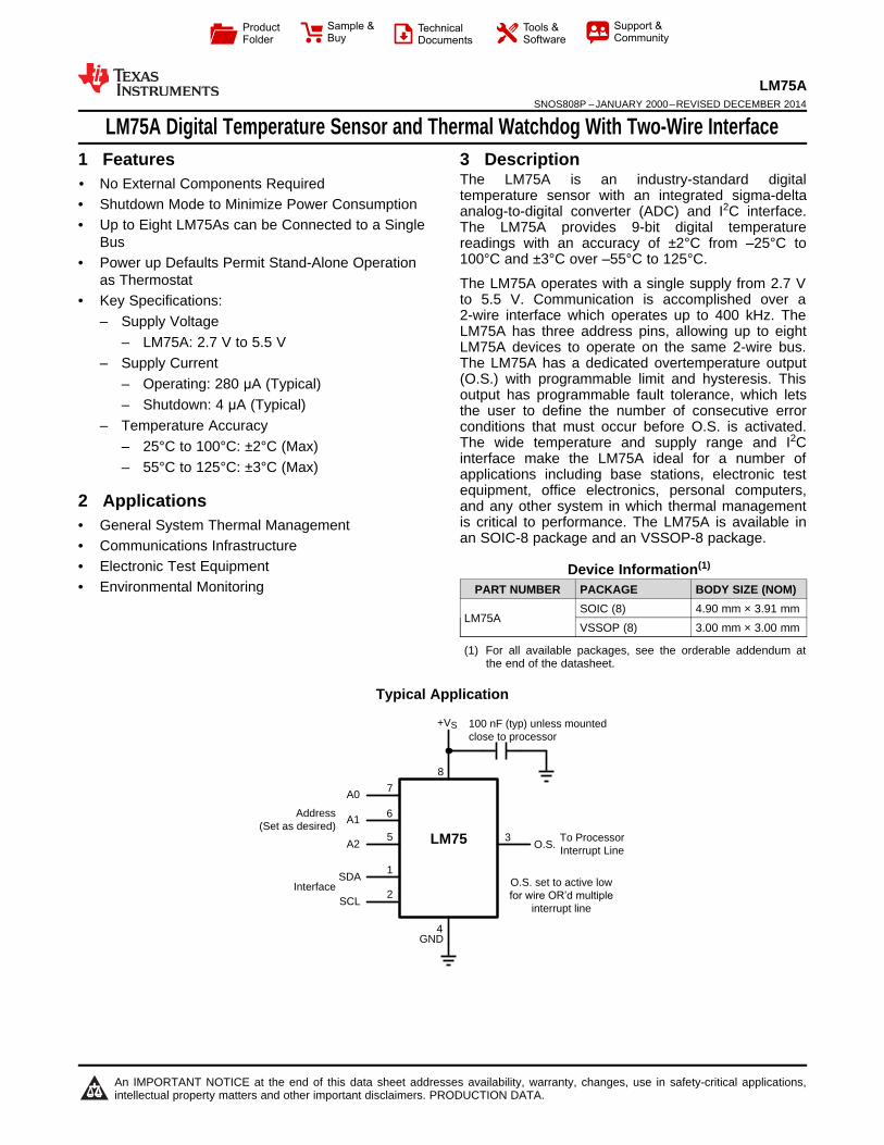
+VS
A0
A1
A2
SCL
SDA
O.S.
GND
8
7
6
5 3
1
2
4
LM75
Address(Set as desired)
To ProcessorInterrupt Line
Interface
100 nF (typ) unless mounted close to processor
O.S. set to active low IRU�ZLUH�25¶G�PXOWLSOH
interrupt line
Product
Folder
Sample &Buy
Technical
Documents
Tools &
Software
Support &Community
LM75ASNOS808P –JANUARY 2000–REVISED DECEMBER 2014
LM75A Digital Temperature Sensor and Thermal Watchdog With Two-Wire Interface1 Features 3 Description
The LM75A is an industry-standard digital1• No External Components Required
temperature sensor with an integrated sigma-delta• Shutdown Mode to Minimize Power Consumption analog-to-digital converter (ADC) and I2C interface.• Up to Eight LM75As can be Connected to a Single The LM75A provides 9-bit digital temperature
Bus readings with an accuracy of ±2°C from –25°C to100°C and ±3°C over –55°C to 125°C.• Power up Defaults Permit Stand-Alone Operation
as Thermostat The LM75A operates with a single supply from 2.7 Vto 5.5 V. Communication is accomplished over a• Key Specifications:2-wire interface which operates up to 400 kHz. The– Supply VoltageLM75A has three address pins, allowing up to eight
– LM75A: 2.7 V to 5.5 V LM75A devices to operate on the same 2-wire bus.The LM75A has a dedicated overtemperature output– Supply Current(O.S.) with programmable limit and hysteresis. This– Operating: 280 μA (Typical)output has programmable fault tolerance, which lets
– Shutdown: 4 μA (Typical) the user to define the number of consecutive error– Temperature Accuracy conditions that must occur before O.S. is activated.
The wide temperature and supply range and I2C– 25°C to 100°C: ±2°C (Max)interface make the LM75A ideal for a number of– 55°C to 125°C: ±3°C (Max) applications including base stations, electronic testequipment, office electronics, personal computers,2 Applications and any other system in which thermal managementis critical to performance. The LM75A is available in• General System Thermal Managementan SOIC-8 package and an VSSOP-8 package.• Communications Infrastructure
• Electronic Test Equipment Device Information(1)
• Environmental Monitoring PART NUMBER PACKAGE BODY SIZE (NOM)SOIC (8) 4.90 mm × 3.91 mm
LM75AVSSOP (8) 3.00 mm × 3.00 mm
(1) For all available packages, see the orderable addendum atthe end of the datasheet.
Typical Application
1
An IMPORTANT NOTICE at the end of this data sheet addresses availability, warranty, changes, use in safety-critical applications,intellectual property matters and other important disclaimers. PRODUCTION DATA.

LM75ASNOS808P –JANUARY 2000–REVISED DECEMBER 2014 www.ti.com
Table of Contents7.3 Feature Description................................................. 101 Features .................................................................. 17.4 Device Functional Modes........................................ 102 Applications ........................................................... 17.5 Programming........................................................... 113 Description ............................................................. 17.6 Register Maps ......................................................... 134 Revision History..................................................... 2
8 Application and Implementation ........................ 155 Pin Configuration and Functions ......................... 38.1 Application Information............................................ 156 Specifications......................................................... 38.2 Typical Applications ................................................ 156.1 Absolute Maximum Ratings ...................................... 38.3 System Examples ................................................... 166.2 ESD Ratings.............................................................. 3
9 Power Supply Recommendations ...................... 186.3 Recommended Operating Conditions....................... 410 Layout................................................................... 186.4 Thermal Information .................................................. 4
10.1 Layout Guidelines ................................................. 186.5 Temperature-to-Digital Converter Characteristics..... 410.2 Layout Example .................................................... 196.6 Digital DC Characteristics ......................................... 5
11 Device and Documentation Support ................. 206.7 I2C Digital Switching Characteristics......................... 511.1 Trademarks ........................................................... 206.8 Typical Characteristics .............................................. 911.2 Electrostatic Discharge Caution............................ 207 Detailed Description ............................................ 1011.3 Glossary ................................................................ 207.1 Overview ................................................................. 10
12 Mechanical, Packaging, and Orderable7.2 Functional Block Diagram ....................................... 10Information ........................................................... 20
4 Revision HistoryNOTE: Page numbers for previous revisions may differ from page numbers in the current version.
Changes from Revision O (May 2013) to Revision P Page
• Added Pin Configuration and Functions section, ESD Ratings table, Feature Description section, Device FunctionalModes, Application and Implementation section, Power Supply Recommendations section, Layout section, Deviceand Documentation Support section, and Mechanical, Packaging, and Orderable Information section .............................. 1
Changes from Revision N (May 2013) to Revision O Page
• Changed layout of National Data Sheet to TI format ........................................................................................................... 16
2 Submit Documentation Feedback Copyright © 2000–2014, Texas Instruments Incorporated
Product Folder Links: LM75A
LM75Awww.ti.com SNOS808P –JANUARY 2000–REVISED DECEMBER 2014
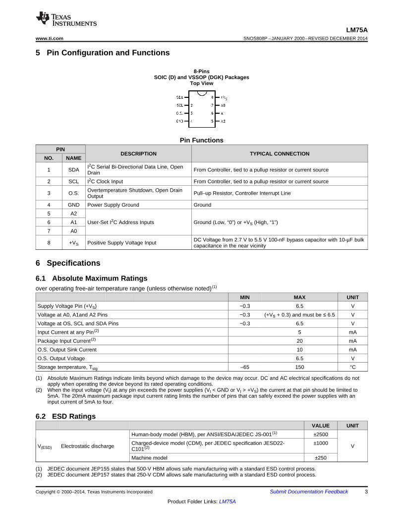
5 Pin Configuration and Functions
8-PinsSOIC (D) and VSSOP (DGK) Packages
Top View
Pin FunctionsPIN
DESCRIPTION TYPICAL CONNECTIONNO. NAME
I2C Serial Bi-Directional Data Line, Open1 SDA From Controller, tied to a pullup resistor or current sourceDrain2 SCL I2C Clock Input From Controller, tied to a pullup resistor or current source
Overtemperature Shutdown, Open Drain3 O.S. Pull–up Resistor, Controller Interrupt LineOutput4 GND Power Supply Ground Ground5 A26 A1 User-Set I2C Address Inputs Ground (Low, “0”) or +VS (High, “1”)7 A0
DC Voltage from 2.7 V to 5.5 V 100-nF bypass capacitor with 10-µF bulk8 +VS Positive Supply Voltage Input capacitance in the near vicinity
6 Specifications
6.1 Absolute Maximum Ratingsover operating free-air temperature range (unless otherwise noted) (1)
MIN MAX UNITSupply Voltage Pin (+VS) −0.3 6.5 VVoltage at A0, A1and A2 Pins −0.3 (+VS + 0.3) and must be ≤ 6.5 VVoltage at OS, SCL and SDA Pins −0.3 6.5 VInput Current at any Pin (2) 5 mAPackage Input Current (2) 20 mAO.S. Output Sink Current 10 mAO.S. Output Voltage 6.5 VStorage temperature, Tstg –65 150 °C
(1) Absolute Maximum Ratings indicate limits beyond which damage to the device may occur. DC and AC electrical specifications do notapply when operating the device beyond its rated operating conditions.
(2) When the input voltage (VI) at any pin exceeds the power supplies (VI < GND or VI > +VS) the current at that pin should be limited to5mA. The 20mA maximum package input current rating limits the number of pins that can safely exceed the power supplies with aninput current of 5mA to four.
6.2 ESD RatingsVALUE UNIT
Human-body model (HBM), per ANSI/ESDA/JEDEC JS-001 (1) ±2500Charged-device model (CDM), per JEDEC specification JESD22- ±1000V(ESD) Electrostatic discharge VC101 (2)
Machine model ±250
(1) JEDEC document JEP155 states that 500-V HBM allows safe manufacturing with a standard ESD control process.(2) JEDEC document JEP157 states that 250-V CDM allows safe manufacturing with a standard ESD control process.
Copyright © 2000–2014, Texas Instruments Incorporated Submit Documentation Feedback 3
Product Folder Links: LM75A

LM75ASNOS808P –JANUARY 2000–REVISED DECEMBER 2014 www.ti.com
6.3 Recommended Operating Conditions (1) (2)
MIN MAX UNITSpecified Temperature Range (TMIN to TMAX) −55 125 °CSupply Voltage Range (+VS) LM75A 2.7 5.5 V
(1) LM75A θJA (thermal resistance, junction-to-ambient) when attached to a printed circuit board with 2 oz. foil similar to the one shown inThermal Information is summarized in the table below the Operating Ratings table.
(2) Reflow temperature profiles are different for lead-free and non-lead-free packages. Soldering process must comply with ReflowTemperature Profile specifications. Refer to www.ti.com/packaging.(2)
6.4 Thermal InformationLM75A
THERMAL METRIC (1) D DGK UNIT8 PINS 8 PINS
RθJA Junction-to-ambient thermal resistance 200 250 °C/W
(1) For more information about traditional and new thermal metrics, see the IC Package Thermal Metrics application report, SPRA953.
6.5 Temperature-to-Digital Converter CharacteristicsUnless otherwise noted, these specifications apply for: +VS = 2.7 to 5.5 Vdc for LM75AIM. TA = TJ = 25°C, unless otherwisenoted.
PARAMETER TEST CONDITIONS MIN TYP (1) MAX (2) UNITTA = −25°C to +100°C –2 2–55°C ≤ TJ ≤ 125°C
Accuracy °CTA = −55°C to +125°C –3 3–55°C ≤ TJ ≤ 125°C
Resolution 9 BitsTemperature Conversion Time See (3) 100
msSee (3), –55°C ≤ TJ ≤ 125°C 300I2C Inactive 0.28
mAI2C Inactive, –55°C ≤ TJ ≤ 125°C 0.5
Quiescent Current LM75AShutdown Mode, +VS = 3 V 4 μAShutdown Mode, +VS = 5 V 6 μA
O.S. Output Saturation Voltage IOUT = 4 mA, –55°C ≤ TJ ≤ 125°C 0.8 VO.S. Delay See (4), –55°C ≤ TJ ≤ 125°C 1 6 ConversionTOS Default Temperature See (5) 80 °CTHYST Default Temperature See (5) 75 °C
(1) Typicals are at TA = 25°C and represent most likely parametric norm.(2) Maximum values (limits) are ensured to AOQL (Average Outgoing Quality Level).(3) The conversion-time specification is provided to indicate how often the temperature data is updated. The LM75A can be accessed at
any time and reading the Temperature Register will yield result from the last temperature conversion. When the LM75A is accessed, theconversion that is in process will be interrupted and it will be restarted after the end of the communication. Accessing the LM75Acontinuously without waiting at least one conversion time between communications will prevent the device from updating theTemperature Register with a new temperature conversion result. Consequently, the LM75A should not be accessed continuously with await time of less than 300ms.
(4) O.S. Delay is user programmable up to 6 “over limit” conversions before O.S. is set to minimize false tripping in noisy environments.(5) Default values set at power up.
4 Submit Documentation Feedback Copyright © 2000–2014, Texas Instruments Incorporated
Product Folder Links: LM75A

LM75Awww.ti.com SNOS808P –JANUARY 2000–REVISED DECEMBER 2014
6.6 Digital DC CharacteristicsUnless otherwise noted, these specifications apply for +VS = 2.7 to 5.5 Vdc for LM75AIM and LM75AIMM. TA = TJ = 25°C,unless otherwise noted.
PARAMETER TEST CONDITIONS MIN TYP (1) MAX (2) UNIT–55°C ≤ TJ ≤ 125°C +VS × 0.7 V
VIN(1) Logical “1” Input Voltage +VS + 0.3V
–55°C ≤ TJ ≤ 125°C −0.3 VVIN(0) Logical “0” Input Voltage +VS × 0.3
VVIN = +VS 0.005
IIN(1) Logical “1” Input Current μAVIN = +VS, –55°C ≤ 1.0TJ ≤ 125°CVIN = 0 V −0.005
IIN(0) Logical “0” Input Current μAVIN = 0 V, –55°C ≤ −1.0TJ ≤ 125°C
CIN All Digital Inputs 5 pFHigh Level Output VOH = 5 V, –55°C ≤IOH Current LM75A 1 μATJ ≤ 125°COpen drain leakage
IOL = 3 mA, –55°C ≤ 0.4VOL Low Level Output Voltage VTJ ≤ 125°CCL = 400 pF IO = 3 250
tOF Output Fall Time mA, –55°C ≤ TJ ≤ ns125°C
(1) Typicals are at TA = 25°C and represent most likely parametric norm.(2) Maximum values (limits) are ensured to AOQL (Average Outgoing Quality Level).
6.7 I2C Digital Switching CharacteristicsUnless otherwise noted, these specifications apply for +VS = 2.7 to 5.5 Vdc for LM75AIM and LM75AIMM on output lines = 80pF unless otherwise specified. TA = TJ = 25°C, unless otherwise noted.
PARAMETER TEST CONDITIONS MIN TYP (1) MAX (2) (3) UNITt1 SCL (Clock) Period –55°C ≤ TJ ≤ 125°C 2.5 nst2 Data in Set-Up Time to SCL High –55°C ≤ TJ ≤ 125°C 100 nst3 Data Out Stable after SCL Low –55°C ≤ TJ ≤ 125°C 0 nst4 SDA Low Set-Up Time to SCL Low (Start –55°C ≤ TJ ≤ 125°C 100 nsCondition)t5 SDA High Hold Time after SCL High (Stop –55°C ≤ TJ ≤ 125°C 100 nsCondition)
75SDA Time Low for Reset of SerialtTIMEOUT LM75A msInterface (4) –55°C ≤ TJ ≤ 125°C 325
(1) Typicals are at TA = 25°C and represent most likely parametric norm.(2) Maximum values (limits) are ensured to AOQL (Average Outgoing Quality Level).(3) Timing specifications are tested at the bus input logic levels (Vin(0)=0.3XVA for a falling edge and Vin(1)=0.7XVA for a rising edge)
when the SCL and SDA edge rates are similar.(4) Holding the SDA line low for a time greater than tTIMEOUT will cause the LM75A to reset SDA to the IDLE state of the serial bus
communication (SDA set High).
Copyright © 2000–2014, Texas Instruments Incorporated Submit Documentation Feedback 5
Product Folder Links: LM75A

LM75ASNOS808P –JANUARY 2000–REVISED DECEMBER 2014 www.ti.com
Figure 1. Timing Diagram
Figure 2. Temperature-to-Digital Transfer Function (Non-Linear Scale for Clarity)
Figure 3. Printed Circuit Board Used for Thermal Resistance Specifications
6 Submit Documentation Feedback Copyright © 2000–2014, Texas Instruments Incorporated
Product Folder Links: LM75A
LM75Awww.ti.com SNOS808P –JANUARY 2000–REVISED DECEMBER 2014
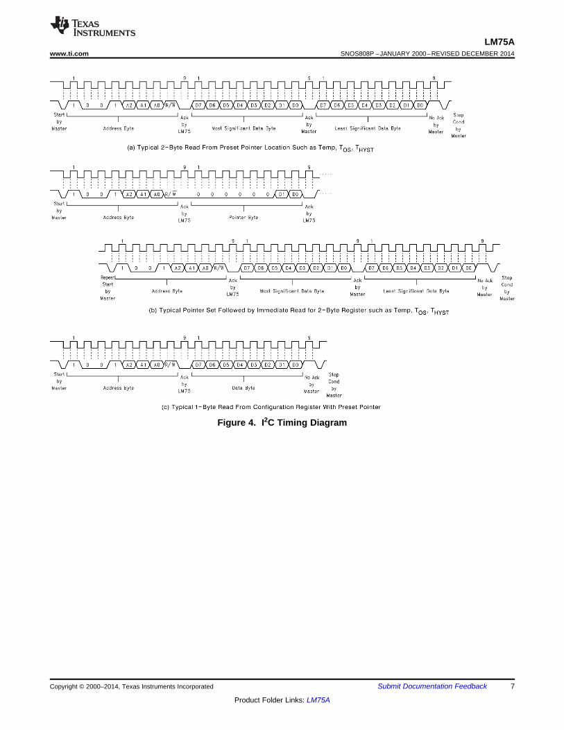
Figure 4. I2C Timing Diagram
Copyright © 2000–2014, Texas Instruments Incorporated Submit Documentation Feedback 7
Product Folder Links: LM75A

LM75ASNOS808P –JANUARY 2000–REVISED DECEMBER 2014 www.ti.com
Figure 5. I2C Timing Diagrams (Continued)
8 Submit Documentation Feedback Copyright © 2000–2014, Texas Instruments Incorporated
Product Folder Links: LM75A

LM75Awww.ti.com SNOS808P –JANUARY 2000–REVISED DECEMBER 2014
6.8 Typical Characteristics
Figure 6. Accuracy vs Temperature (LM75A)
Copyright © 2000–2014, Texas Instruments Incorporated Submit Documentation Feedback 9
Product Folder Links: LM75A

7
6
5
A0
A1
A2
Temperature
Threshold
Silicon Bandgap Temperature
Sensor
Ð
1-BitD/A
10-BitDigital
Decimation Filter
9-Bit Sigma-Delta ADC
Configuration Register
TOS Set Point
Register
PointerRegister
THYST Set
Point Register
Set PointComparator
3O.S.
Reset
1
2
SDA
SCLTwo-Wire Interface
4
8
+VS
GND
Product ID Register
LM75ASNOS808P –JANUARY 2000–REVISED DECEMBER 2014 www.ti.com
7 Detailed Description
7.1 OverviewThe LM75A temperature sensor incorporates a band-gap type temperature sensor and 9-bit ADC (sigma-deltaADC). The temperature data output of the LM75A is available at all times via the I2C bus. If a conversion is inprogress, it will be stopped and restarted after the read. A digital comparator is also incorporated that comparesa series of readings, the number of which is user-selectable, to user-programmable setpoint and hysteresisvalues. The comparator trips the O.S. output line, which is programmable for mode and polarity. The LM75A hasan integrated low-pass filter on both the SDA and the SCL line. These filters increase communications reliabilityin noisy environments.
The LM75A also has a bus fault timeout feature. If the SDA line is held low for longer than tTIMEOUT (seespecification) the LM75A will reset to the IDLE state (SDA set to high impedance) and wait for a new startcondition. The TIMEOUT feature is not functional in Shutdown Mode.
7.2 Functional Block Diagram
7.3 Feature Description
7.3.1 Digital Temperature SensorThe LM75A is an industry-standard digital temperature sensor with an integrated sigma-delta ADC and I2Cinterface. The LM75A provides 9-bit digital temperature readings with an accuracy of ±2°C from –25°C to 100°Cand ±3°C over –55°C to 125°C.
The LM75A operates with a single supply from +2.7 V to +5.5 V. Communication is accomplished over a 2-wireinterface which operates up to 400kHz. The LM75A has three address pins, allowing up to eight LM75A devicesto operate on the same 2-wire bus. The LM75A has a dedicated over-temperature output (O.S.) withprogrammable limit and hysteresis. This output has programmable fault tolerance, which allows the user todefine the number of consecutive error conditions that must occur before O.S. is activated.
7.4 Device Functional ModesIn Comparator mode the O.S. Output behaves like a thermostat. The output becomes active when temperatureexceeds the TOS limit, and leaves the active state when the temperature drops below the THYST limit. In this modethe O.S. output can be used to turn a cooling fan on, initiate an emergency system shutdown, or reduce systemclock speed. Shutdown mode does not reset O.S. state in a comparator mode.
In Interrupt mode exceeding TOS also makes O.S. active but O.S. will remain active indefinitely until reset byreading any register via the I2C interface. Once O.S. has been activated by crossing TOS, then reset, it can beactivated again only by Temperature going below THYST. Again, it will remain active indefinitely until being resetby a read. Placing the LM75A in shutdown mode also resets the O.S. Output.
10 Submit Documentation Feedback Copyright © 2000–2014, Texas Instruments Incorporated
Product Folder Links: LM75A

LM75Awww.ti.com SNOS808P –JANUARY 2000–REVISED DECEMBER 2014
Device Functional Modes (continued)The LM75A always powers up in a known state. The power up default conditions are:• Comparator mode• TOS = 80°C• THYST = 75°C• O.S. active low• Pointer = “00”
When the supply voltage is less than about 1.7V, the LM75A is considered powered down. As the supply voltagerises above the nominal 1.7V power up threshold, the internal registers are reset to the power up default valueslisted above.
If the LM75A is not connected to the I2C bus on power up, it will act as a stand-alone thermostat with the powerup default conditions listed above. It is optional, but recommended, to connect the address pins (A2, A1, A0) andthe SCL and SDA pins together and to a 10k pullup resistor to +VS for better noise immunity. Any of these pinsmay also be tied high separately through a 10-k pullup resistor.
7.5 Programming
7.5.1 I2C Bus InterfaceThe LM75A operates as a slave on the I2C bus, so the SCL line is an input (no clock is generated by the LM75A)and the SDA line is a bi-directional serial data path. According to I2C bus specifications, the LM75A has a 7-bitslave address. The four most significant bits of the slave address are hard wired inside the LM75A and are“1001”. The three least significant bits of the address are assigned to pins A2–A0, and are set by connectingthese pins to ground for a low, (0); or to +VS for a high, (1).
Therefore, the complete slave address is:
1 0 0 1 A2 A1 A0MSB LSB
These interrupt mode resets of O.S. occur only when LM75A is read or placed in shutdown. Otherwise, O.S. wouldremain active indefinitely for any event.
Figure 7. O.S. Output Temperature Response Diagram
Copyright © 2000–2014, Texas Instruments Incorporated Submit Documentation Feedback 11
Product Folder Links: LM75A
LM75ASNOS808P –JANUARY 2000–REVISED DECEMBER 2014 www.ti.com
7.5.2 Temperature Data FormatTemperature data can be read from the Temperature, TOS Set Point, and THYST Set Point registers; and written tothe TOS Set Point, and THYST Set Point registers. Temperature data is represented by a 9-bit, two's complementword with an LSB (Least Significant Bit) equal to 0.5°C:
Digital OutputTemperature
Binary Hex+125°C 0 1111 1010 0FAh+25°C 0 0011 0010 032h+0.5°C 0 0000 0001 001h
0°C 0 0000 0000 000h−0.5°C 1 1111 1111 1FFh−25°C 1 1100 1110 1CEh−55°C 1 1001 0010 192h
7.5.3 Shutdown ModeShutdown mode is enabled by setting the shutdown bit in the Configuration register via the I2C bus. Shutdownmode reduces power supply current significantly. See specified quiescent current specification in the electricaltables. In Interrupt mode O.S. is reset if previously set and is undefined in Comparator mode during shutdown.The I2C interface remains active. Activity on the clock and data lines of the I2C bus may slightly increaseshutdown mode quiescent current. TOS, THYST, and Configuration registers can be read from and written to inshutdown mode.
For the LM75A, the TIMEOUT feature is turned off in Shutdown Mode.
7.5.4 Fault QueueA fault queue of up to 6 faults is provided to prevent false tripping of O.S. when the LM75A is used in noisyenvironments. The number of faults set in the queue must occur consecutively to set the O.S. output.
7.5.5 Comparator and Interrupt ModeAs indicated in the O.S. Output Temperature Response Diagram, Figure 7, the events that trigger O.S. areidentical for either Comparator or Interrupt mode. The most important difference is that in Interrupt mode the O.S.will remain set indefinitely once it has been set. To reset O.S. while in Interrupt mode, perform a read from anyregister in the LM75A.
7.5.6 O.S. OutputThe O.S. output is an open-drain output and does not have an internal pullup. A “high” level will not be observedon this pin until pullup current is provided from some external source, typically a pullup resistor. Choice ofresistor value depends on many system factors but, in general, the pullup resistor should be as large as possible.This will minimize any errors due to internal heating of the LM75A. The maximum resistance of the pullup, basedon LM75A specification for High Level Output Current, to provide a 2-V high level, is 30 kΩ.
7.5.7 O.S. PolarityThe O.S. output can be programmed via the configuration register to be either active low (default mode), oractive high. In active low mode the O.S. output goes low when triggered exactly as shown on the O.S. OutputTemperature Response Diagram, Figure 7. Active high simply inverts the polarity of the O.S. output.
12 Submit Documentation Feedback Copyright © 2000–2014, Texas Instruments Incorporated
Product Folder Links: LM75A

I2C Interface
SDA
SCL
Pointer Register(Selects register for
communication)
AddressData
Temperature(Read-Only)
Pointer = 00000000
Product ID (Read-Only)
Pointer = 00000111
TOS Set Point(Read-Write)
Pointer = 00000011
Configuration(Read-Write)
Pointer = 00000001
THYST Set Point(Read-Write)
Pointer = 00000010
LM75Awww.ti.com SNOS808P –JANUARY 2000–REVISED DECEMBER 2014
7.5.8 Internal Register Structure
Figure 8. Register Structure
There are four data registers in the LM75A and an additional Product ID register selected by the Pointer register.At power-up the Pointer is set to “000”; the location for the Temperature Register. The Pointer register latcheswhatever the last location it was set to. In Interrupt Mode, a read from the LM75A, or placing the device inshutdown mode, resets the O.S. output. All registers are read and write, except the Temperature register and theLM75A's Product ID register, which are read-only.
A write to the LM75A will always include the address byte and the Pointer byte. A write to the Configurationregister requires one data byte, and the TOS and THYST registers require two data bytes.
Reading the LM75A can take place either of two ways: If the location latched in the Pointer is correct (most of thetime it is expected that the Pointer will point to the Temperature register because it will be the data mostfrequently read from the LM75A), then the read can simply consist of an address byte, followed by retrieving thecorresponding number of data bytes. If the Pointer needs to be set, then an address byte, pointer byte, repeatstart, and another address byte will accomplish a read.
The first data byte is the most significant byte with most significant bit first, permitting only as much data asnecessary to be read to determine temperature condition. For instance, if the first four bits of the temperaturedata indicates an overtemperature condition, the host processor could immediately take action to remedy theexcessive temperatures. At the end of a read, the LM75A can accept either Acknowledge or No Acknowledgefrom the Master (No Acknowledge is typically used as a signal for the slave that the Master has read its lastbyte).
7.6 Register Maps
7.6.1 Pointer Register (Selects Which Registers Will Be Read From or Written to):
P7 P6 P5 P4 P3 P2 P1 P00 0 0 0 0 Register Select
P0-P1: Register Select:
P2 P1 P0 Register0 0 0 Temperature (Read-only) (Power-up default)0 0 1 Configuration (Read/Write)0 1 0 THYST (Read/Write)0 1 1 TOS (Read/Write)1 1 1 Product ID Register
Copyright © 2000–2014, Texas Instruments Incorporated Submit Documentation Feedback 13
Product Folder Links: LM75A

LM75ASNOS808P –JANUARY 2000–REVISED DECEMBER 2014 www.ti.com
P3–P7: Must be kept zero.
7.6.2 Temperature Register (Read-Only):
D15 D14 D13 D12 D11 D10 D9 D8 D7 D6 D5 D4 D3 D2 D1 D0MSB Bit 7 Bit 6 Bit 5 Bit 4 Bit 3 Bit 2 Bit 1 LSB X X X X X X X
D0–D6: Undefined. D7–D15: Temperature Data. One LSB = 0.5°C. Two's complement format.
7.6.3 Configuration Register (Read/Write):
D7 D6 D5 D4 D3 D2 D1 D00 0 0 Fault Queue O.S. Polarity Cmp/Int Shutdown
Power up default is with all bits “0” (zero).
D0: Shutdown: When set to 1 the LM75A goes to low power shutdown mode.
D1: Comparator/Interrupt mode: 0 is Comparator mode, 1 is Interrupt mode.
D2: O.S. Polarity: 0 is active low, 1 is active high. O.S. is an open-drain output under all conditions.
D3–D4: Fault Queue: Number of faults necessary to detect before setting O.S. output to avoid false tripping dueto noise. Faults are determine at the end of a conversion. See specified temperature conversion time in theelectrical tables.
D4 D3 Number of Faults0 0 1 (Power-up default)0 1 21 0 41 1 6
D5–D7: These bits are used for production testing and must be kept zero for normal operation.
7.6.4 THYST and TOS Register (Read/Write):
D15 D14 D13 D12 D11 D10 D9 D8 D7 D6 D5 D4 D3 D2 D1 D0MSB Bit 7 Bit 6 Bit 5 Bit 4 Bit 3 Bit 2 Bit 1 LSB X X X X X X X
D0–D6: Undefined D7–D15: THYST Or TOS Trip Temperature Data. Power up default is TOS = 80°C, THYST =75°C
7.6.5 PRODID: Product ID Register (Read-Only) Pointer Address: 07h
D7 D6 D5 D4 D3 D2 D1 D01 0 1 0 0 0 0 1
D4--D7 Product Identification Nibble. Always returns Ah to uniquely identify this part as the LM75A.
D0--D3 Die Revision Nibble. Returns 1h to uniquely identify the revision level as one.
14 Submit Documentation Feedback Copyright © 2000–2014, Texas Instruments Incorporated
Product Folder Links: LM75A

+VS
O.S.
GND
8
3
4
LM75A
C1100 nF
+12V
+12V/300 mAFan Motor
R110k
R210k
Q2NDP410Aseries
Q12N3904
R310k
7
6
5
1
2
A0
A1
A2
SCL
SDA
Optional butRecommended
Pull-upIn Stand-alone
Mode
LM75Awww.ti.com SNOS808P –JANUARY 2000–REVISED DECEMBER 2014
8 Application and Implementation
NOTEInformation in the following applications sections is not part of the TI componentspecification, and TI does not warrant its accuracy or completeness. TI’s customers areresponsible for determining suitability of components for their purposes. Customers shouldvalidate and test their design implementation to confirm system functionality.
8.1 Application InformationThe wide temperature and supply range and I2C interface make the LM75A ideal for a number of applicationsincluding base stations, electronic test equipment, office electronics, personal computers, and any other systemwhere thermal management is critical to performance.
8.2 Typical Applications
8.2.1 Simple Fan Controller, Interface Optional
When using the two-wire interface: program O.S. for active high and connect O.S. directly to Q2's gate.
Figure 9. Simple Fan Controller, Interface Optional
8.2.1.1 Design RequirementsThe LM75A requires positive supply voltage of 2.7 V to 5.5 V to be applied between +Vs and GND. For bestresults, bypass capacitors of 100 nF and 10 µF are recommended. Pullup resistors of 10 kΩ are required on SCLand SDA.
8.2.1.2 Detailed Design ProcedureAccessing the conversion result of the LM75A consists of writing an address byte followed by retrieving thecorresponding number of data bytes. The first data byte is the most significant byte with the most significant bitfirst, permitting only as much data as necessary to be read to determine temperature condition. For instance, ifthe first four bits of the temperature data indicates an overtemperature condition, the host processor couldimmediately take action to remedy the excessive temperatures. At the end of a read, the LM75A can accepteither Acknowledge or No Acknowledge from the Master (No Acknowledge is typically used as a signal for theslave that the Master has read its last byte). Temperature data is two's complement format and one LSB isequivalent to 0.5°C.
Copyright © 2000–2014, Texas Instruments Incorporated Submit Documentation Feedback 15
Product Folder Links: LM75A
+ 5 VDC
O.S.
GND
8
3
4
LM75A
R110k
Q12N2222A
K15V Relay
HeaterHeaterSupply
D11N4001
R210k
7
6
5
1
2
A0
A1
A2
SCL
SDA
Optional butRecommended
Pull-up In Stand-alone
Mode
C1100 nF
+VS
LM75ASNOS808P –JANUARY 2000–REVISED DECEMBER 2014 www.ti.com
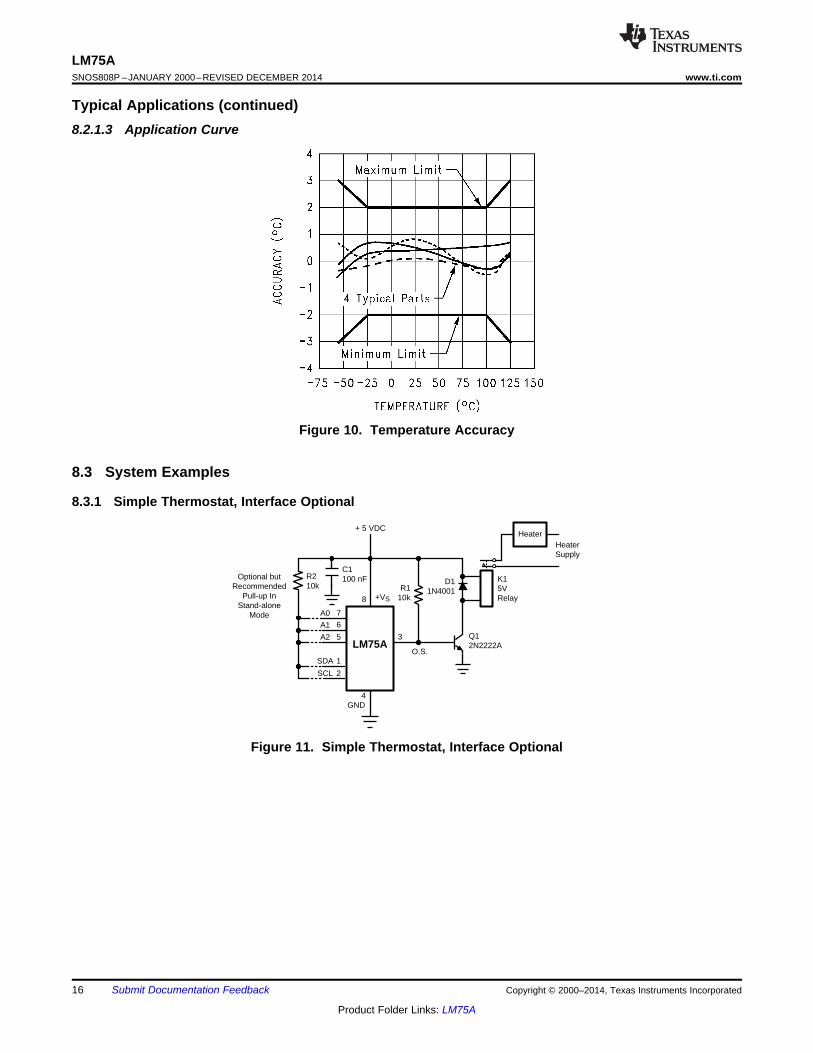
Typical Applications (continued)8.2.1.3 Application Curve
Figure 10. Temperature Accuracy
8.3 System Examples
8.3.1 Simple Thermostat, Interface Optional
Figure 11. Simple Thermostat, Interface Optional
16 Submit Documentation Feedback Copyright © 2000–2014, Texas Instruments Incorporated
Product Folder Links: LM75A
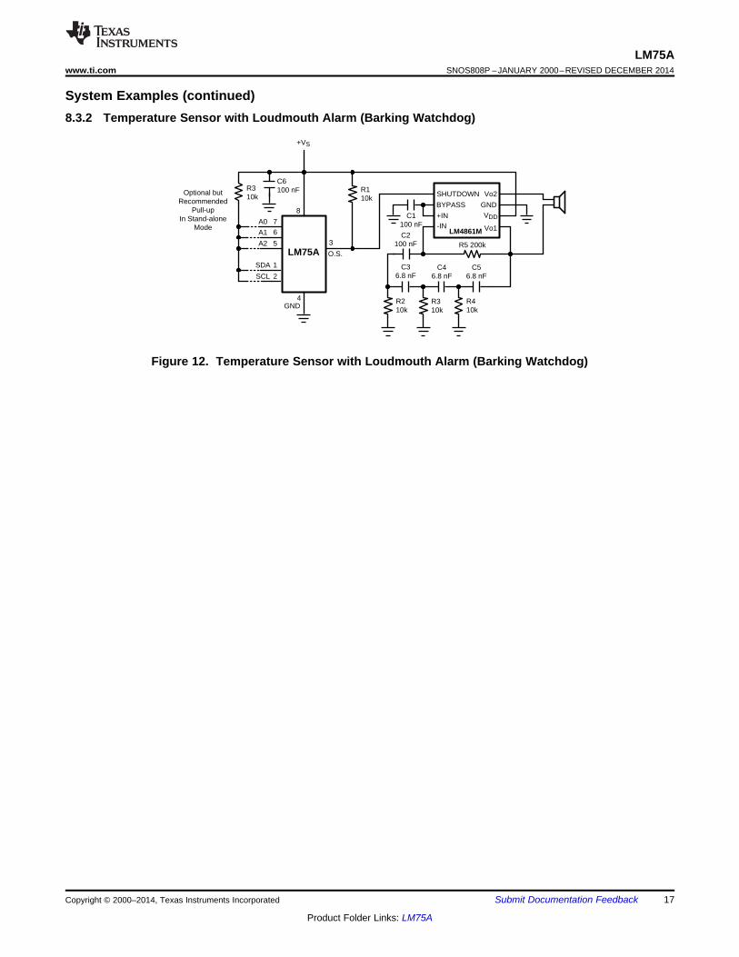
+VS
O.S.
GND
8
3
4
LM75A
C6100 nF R1
10kR310k
7
6
5
1
2
A0
A1
A2
SCL
SDA
Optional butRecommended
Pull-upIn Stand-alone
Mode
SHUTDOWN
BYPASS
+IN-IN
C2100 nF
C1100 nF
R5 200k
R210k
R310k
R410k
C36.8 nF
C46.8 nF
C56.8 nF
GND
Vo2
Vo1
VDD
LM4861M
LM75Awww.ti.com SNOS808P –JANUARY 2000–REVISED DECEMBER 2014
System Examples (continued)8.3.2 Temperature Sensor with Loudmouth Alarm (Barking Watchdog)
Figure 12. Temperature Sensor with Loudmouth Alarm (Barking Watchdog)
Copyright © 2000–2014, Texas Instruments Incorporated Submit Documentation Feedback 17
Product Folder Links: LM75A

LM75ASNOS808P –JANUARY 2000–REVISED DECEMBER 2014 www.ti.com
9 Power Supply RecommendationsThe LM75A is specified for operation from 2.7 V to 5.5 V. Place 100-nF and 10-µF capacitors close to +Vs inorder to reduce errors coupling in from noisy or high impedance supplies.
10 Layout
10.1 Layout GuidelinesTo achieve the expected results when measuring temperature with an integrated circuit temperature sensor likethe LM75A, it is important to understand that the sensor measures its own die temperature. For the LM75A, thebest thermal path between the die and the outside world is through the LM75A's pins. In the VSSOP-8 package,the GND pin is directly connected to the die, so the GND pin provides the best thermal path. If the other pins areat different temperatures (unlikely, but possible), they will affect the die temperature, but not as strongly as theGND pin. In the SOIC-8 package, none of the pins is directly connected to the die, so they will all contributesimilarly to the die temperature. Because the pins represent a good thermal path to the LM75A die, the LM75Awill provide an accurate measurement of the temperature of the printed circuit board on which it is mounted.There is a less efficient thermal path between the plastic package and the LM75A die. If the ambient airtemperature is significantly different from the printed circuit board temperature, it will have a small effect on themeasured temperature.
In probe-type applications, the LM75A can be mounted inside a sealed-end metal tube, and can then be dippedinto a bath or screwed into a threaded hole in a tank. As with any IC, the LM75A and accompanying wiring andcircuits must be kept insulated and dry, to avoid leakage and corrosion. This is especially true if the circuit mayoperate at cold temperatures where condensation can occur. Printed-circuit coatings and varnishes such asHumiseal and epoxy paints or dips are often used to insure that moisture cannot corrode the LM75A or itsconnections.
10.1.1 Digital Noise IssuesThe LM75A features an integrated low-pass filter on both the SCL and the SDA digital lines to mitigate theeffects of bus noise. Although this filtering makes the LM75A communication robust in noisy environments, goodlayout practices are always recommended. Minimize noise coupling by keeping digital traces away fromswitching power supplies. Also, ensure that digital lines containing high-speed data communications cross atright angles to the SDA and SCL lines. Excessive noise coupling into the SDA and SCL lines on theLM75A—specifically noise with amplitude greater than 400 mVpp (the LM75A’s typical hysteresis), overshootgreater than 300mV above +Vs, and undershoot more than 300 mV below GND—may prevent successful serialcommunication with the LM75A. Serial bus no-acknowledge is the most common symptom, causing unnecessarytraffic on the bus. Although the serial bus maximum frequency of communication is only 400 kHz, care must betaken to ensure proper termination within a system with long printed circuit board traces or multiple parts on thebus.
18 Submit Documentation Feedback Copyright © 2000–2014, Texas Instruments Incorporated
Product Folder Links: LM75A

LM75Awww.ti.com SNOS808P –JANUARY 2000–REVISED DECEMBER 2014
10.2 Layout Example
Figure 13. Printed Circuit Board Used for Thermal Resistance Specifications
Copyright © 2000–2014, Texas Instruments Incorporated Submit Documentation Feedback 19
Product Folder Links: LM75A

LM75ASNOS808P –JANUARY 2000–REVISED DECEMBER 2014 www.ti.com
11 Device and Documentation Support
11.1 TrademarksAll trademarks are the property of their respective owners.
11.2 Electrostatic Discharge CautionThese devices have limited built-in ESD protection. The leads should be shorted together or the device placed in conductive foamduring storage or handling to prevent electrostatic damage to the MOS gates.
11.3 GlossarySLYZ022 — TI Glossary.
This glossary lists and explains terms, acronyms, and definitions.
12 Mechanical, Packaging, and Orderable InformationThe following pages include mechanical, packaging, and orderable information. This information is the mostcurrent data available for the designated devices. This data is subject to change without notice and revision ofthis document. For browser-based versions of this data sheet, refer to the left-hand navigation.
20 Submit Documentation Feedback Copyright © 2000–2014, Texas Instruments Incorporated
Product Folder Links: LM75A

PACKAGE OPTION ADDENDUM
www.ti.com 23-Jul-2015
Addendum-Page 1
PACKAGING INFORMATION
Orderable Device Status(1)
Package Type PackageDrawing
Pins PackageQty
Eco Plan(2)
Lead/Ball Finish(6)
MSL Peak Temp(3)
Op Temp (°C) Device Marking(4/5)
Samples
LM75AIM/NOPB ACTIVE SOIC D 8 95 Green (RoHS& no Sb/Br)
CU SN Level-1-260C-UNLIM -55 to 125 LM75AIM
LM75AIMM/NOPB ACTIVE VSSOP DGK 8 1000 Green (RoHS& no Sb/Br)
CU SN Level-1-260C-UNLIM -55 to 125 T00A
LM75AIMME/NOPB ACTIVE VSSOP DGK 8 250 Green (RoHS& no Sb/Br)
CU SN Level-1-260C-UNLIM -55 to 125 T00A
LM75AIMMX/NOPB ACTIVE VSSOP DGK 8 3500 Green (RoHS& no Sb/Br)
CU SN Level-1-260C-UNLIM -55 to 125 T00A
LM75AIMX/NOPB ACTIVE SOIC D 8 2500 Green (RoHS& no Sb/Br)
CU SN Level-1-260C-UNLIM -55 to 125 LM75AIM
(1) The marketing status values are defined as follows:ACTIVE: Product device recommended for new designs.LIFEBUY: TI has announced that the device will be discontinued, and a lifetime-buy period is in effect.NRND: Not recommended for new designs. Device is in production to support existing customers, but TI does not recommend using this part in a new design.PREVIEW: Device has been announced but is not in production. Samples may or may not be available.OBSOLETE: TI has discontinued the production of the device.
(2) Eco Plan - The planned eco-friendly classification: Pb-Free (RoHS), Pb-Free (RoHS Exempt), or Green (RoHS & no Sb/Br) - please check http://www.ti.com/productcontent for the latest availabilityinformation and additional product content details.TBD: The Pb-Free/Green conversion plan has not been defined.Pb-Free (RoHS): TI's terms "Lead-Free" or "Pb-Free" mean semiconductor products that are compatible with the current RoHS requirements for all 6 substances, including the requirement thatlead not exceed 0.1% by weight in homogeneous materials. Where designed to be soldered at high temperatures, TI Pb-Free products are suitable for use in specified lead-free processes.Pb-Free (RoHS Exempt): This component has a RoHS exemption for either 1) lead-based flip-chip solder bumps used between the die and package, or 2) lead-based die adhesive used betweenthe die and leadframe. The component is otherwise considered Pb-Free (RoHS compatible) as defined above.Green (RoHS & no Sb/Br): TI defines "Green" to mean Pb-Free (RoHS compatible), and free of Bromine (Br) and Antimony (Sb) based flame retardants (Br or Sb do not exceed 0.1% by weightin homogeneous material)
(3) MSL, Peak Temp. - The Moisture Sensitivity Level rating according to the JEDEC industry standard classifications, and peak solder temperature.
(4) There may be additional marking, which relates to the logo, the lot trace code information, or the environmental category on the device.
(5) Multiple Device Markings will be inside parentheses. Only one Device Marking contained in parentheses and separated by a "~" will appear on a device. If a line is indented then it is a continuationof the previous line and the two combined represent the entire Device Marking for that device.

PACKAGE OPTION ADDENDUM
www.ti.com 23-Jul-2015
Addendum-Page 2
(6) Lead/Ball Finish - Orderable Devices may have multiple material finish options. Finish options are separated by a vertical ruled line. Lead/Ball Finish values may wrap to two lines if the finishvalue exceeds the maximum column width.
Important Information and Disclaimer:The information provided on this page represents TI's knowledge and belief as of the date that it is provided. TI bases its knowledge and belief on informationprovided by third parties, and makes no representation or warranty as to the accuracy of such information. Efforts are underway to better integrate information from third parties. TI has taken andcontinues to take reasonable steps to provide representative and accurate information but may not have conducted destructive testing or chemical analysis on incoming materials and chemicals.TI and TI suppliers consider certain information to be proprietary, and thus CAS numbers and other limited information may not be available for release.
In no event shall TI's liability arising out of such information exceed the total purchase price of the TI part(s) at issue in this document sold by TI to Customer on an annual basis.
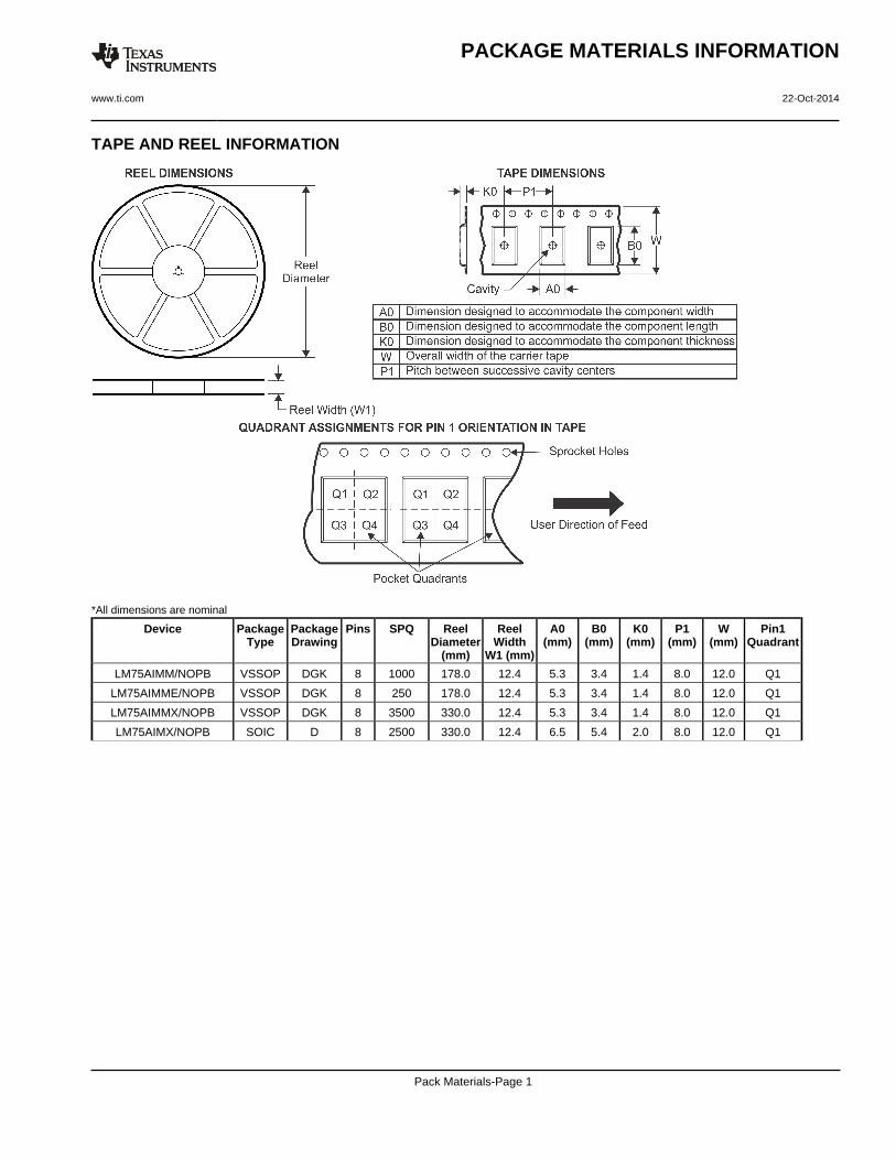
TAPE AND REEL INFORMATION
*All dimensions are nominal
Device PackageType
PackageDrawing
Pins SPQ ReelDiameter
(mm)
ReelWidth
W1 (mm)
A0(mm)
B0(mm)
K0(mm)
P1(mm)
W(mm)
Pin1Quadrant
LM75AIMM/NOPB VSSOP DGK 8 1000 178.0 12.4 5.3 3.4 1.4 8.0 12.0 Q1
LM75AIMME/NOPB VSSOP DGK 8 250 178.0 12.4 5.3 3.4 1.4 8.0 12.0 Q1
LM75AIMMX/NOPB VSSOP DGK 8 3500 330.0 12.4 5.3 3.4 1.4 8.0 12.0 Q1
LM75AIMX/NOPB SOIC D 8 2500 330.0 12.4 6.5 5.4 2.0 8.0 12.0 Q1
PACKAGE MATERIALS INFORMATION
www.ti.com 22-Oct-2014
Pack Materials-Page 1

*All dimensions are nominal
Device Package Type Package Drawing Pins SPQ Length (mm) Width (mm) Height (mm)
LM75AIMM/NOPB VSSOP DGK 8 1000 210.0 185.0 35.0
LM75AIMME/NOPB VSSOP DGK 8 250 210.0 185.0 35.0
LM75AIMMX/NOPB VSSOP DGK 8 3500 367.0 367.0 35.0
LM75AIMX/NOPB SOIC D 8 2500 367.0 367.0 35.0
PACKAGE MATERIALS INFORMATION
www.ti.com 22-Oct-2014
Pack Materials-Page 2


IMPORTANT NOTICE
Texas Instruments Incorporated and its subsidiaries (TI) reserve the right to make corrections, enhancements, improvements and otherchanges to its semiconductor products and services per JESD46, latest issue, and to discontinue any product or service per JESD48, latestissue. Buyers should obtain the latest relevant information before placing orders and should verify that such information is current andcomplete. All semiconductor products (also referred to herein as “components”) are sold subject to TI’s terms and conditions of salesupplied at the time of order acknowledgment.TI warrants performance of its components to the specifications applicable at the time of sale, in accordance with the warranty in TI’s termsand conditions of sale of semiconductor products. Testing and other quality control techniques are used to the extent TI deems necessaryto support this warranty. Except where mandated by applicable law, testing of all parameters of each component is not necessarilyperformed.TI assumes no liability for applications assistance or the design of Buyers’ products. Buyers are responsible for their products andapplications using TI components. To minimize the risks associated with Buyers’ products and applications, Buyers should provideadequate design and operating safeguards.TI does not warrant or represent that any license, either express or implied, is granted under any patent right, copyright, mask work right, orother intellectual property right relating to any combination, machine, or process in which TI components or services are used. Informationpublished by TI regarding third-party products or services does not constitute a license to use such products or services or a warranty orendorsement thereof. Use of such information may require a license from a third party under the patents or other intellectual property of thethird party, or a license from TI under the patents or other intellectual property of TI.Reproduction of significant portions of TI information in TI data books or data sheets is permissible only if reproduction is without alterationand is accompanied by all associated warranties, conditions, limitations, and notices. TI is not responsible or liable for such altereddocumentation. Information of third parties may be subject to additional restrictions.Resale of TI components or services with statements different from or beyond the parameters stated by TI for that component or servicevoids all express and any implied warranties for the associated TI component or service and is an unfair and deceptive business practice.TI is not responsible or liable for any such statements.Buyer acknowledges and agrees that it is solely responsible for compliance with all legal, regulatory and safety-related requirementsconcerning its products, and any use of TI components in its applications, notwithstanding any applications-related information or supportthat may be provided by TI. Buyer represents and agrees that it has all the necessary expertise to create and implement safeguards whichanticipate dangerous consequences of failures, monitor failures and their consequences, lessen the likelihood of failures that might causeharm and take appropriate remedial actions. Buyer will fully indemnify TI and its representatives against any damages arising out of the useof any TI components in safety-critical applications.In some cases, TI components may be promoted specifically to facilitate safety-related applications. With such components, TI’s goal is tohelp enable customers to design and create their own end-product solutions that meet applicable functional safety standards andrequirements. Nonetheless, such components are subject to these terms.No TI components are authorized for use in FDA Class III (or similar life-critical medical equipment) unless authorized officers of the partieshave executed a special agreement specifically governing such use.Only those TI components which TI has specifically designated as military grade or “enhanced plastic” are designed and intended for use inmilitary/aerospace applications or environments. Buyer acknowledges and agrees that any military or aerospace use of TI componentswhich have not been so designated is solely at the Buyer's risk, and that Buyer is solely responsible for compliance with all legal andregulatory requirements in connection with such use.TI has specifically designated certain components as meeting ISO/TS16949 requirements, mainly for automotive use. In any case of use ofnon-designated products, TI will not be responsible for any failure to meet ISO/TS16949.
Products ApplicationsAudio www.ti.com/audio Automotive and Transportation www.ti.com/automotiveAmplifiers amplifier.ti.com Communications and Telecom www.ti.com/communicationsData Converters dataconverter.ti.com Computers and Peripherals www.ti.com/computersDLP® Products www.dlp.com Consumer Electronics www.ti.com/consumer-appsDSP dsp.ti.com Energy and Lighting www.ti.com/energyClocks and Timers www.ti.com/clocks Industrial www.ti.com/industrialInterface interface.ti.com Medical www.ti.com/medicalLogic logic.ti.com Security www.ti.com/securityPower Mgmt power.ti.com Space, Avionics and Defense www.ti.com/space-avionics-defenseMicrocontrollers microcontroller.ti.com Video and Imaging www.ti.com/videoRFID www.ti-rfid.comOMAP Applications Processors www.ti.com/omap TI E2E Community e2e.ti.comWireless Connectivity www.ti.com/wirelessconnectivity
Mailing Address: Texas Instruments, Post Office Box 655303, Dallas, Texas 75265Copyright © 2015, Texas Instruments Incorporated